CN111868894A - Manufacturing method of semiconductor device, substrate processing apparatus, and program - Google Patents
Manufacturing method of semiconductor device, substrate processing apparatus, and programDownload PDFInfo
- Publication number
- CN111868894A CN111868894ACN201880091357.1ACN201880091357ACN111868894ACN 111868894 ACN111868894 ACN 111868894ACN 201880091357 ACN201880091357 ACN 201880091357ACN 111868894 ACN111868894 ACN 111868894A
- Authority
- CN
- China
- Prior art keywords
- flow rate
- film
- gas
- inert gas
- substrate
- Prior art date
- Legal status (The legal status is an assumption and is not a legal conclusion. Google has not performed a legal analysis and makes no representation as to the accuracy of the status listed.)
- Granted
Links
Images


Classifications
- H—ELECTRICITY
- H01—ELECTRIC ELEMENTS
- H01L—SEMICONDUCTOR DEVICES NOT COVERED BY CLASS H10
- H01L21/00—Processes or apparatus adapted for the manufacture or treatment of semiconductor or solid state devices or of parts thereof
- H01L21/02—Manufacture or treatment of semiconductor devices or of parts thereof
- H01L21/02104—Forming layers
- H01L21/02107—Forming insulating materials on a substrate
- H01L21/02109—Forming insulating materials on a substrate characterised by the type of layer, e.g. type of material, porous/non-porous, pre-cursors, mixtures or laminates
- H01L21/02112—Forming insulating materials on a substrate characterised by the type of layer, e.g. type of material, porous/non-porous, pre-cursors, mixtures or laminates characterised by the material of the layer
- H01L21/02123—Forming insulating materials on a substrate characterised by the type of layer, e.g. type of material, porous/non-porous, pre-cursors, mixtures or laminates characterised by the material of the layer the material containing silicon
- C—CHEMISTRY; METALLURGY
- C23—COATING METALLIC MATERIAL; COATING MATERIAL WITH METALLIC MATERIAL; CHEMICAL SURFACE TREATMENT; DIFFUSION TREATMENT OF METALLIC MATERIAL; COATING BY VACUUM EVAPORATION, BY SPUTTERING, BY ION IMPLANTATION OR BY CHEMICAL VAPOUR DEPOSITION, IN GENERAL; INHIBITING CORROSION OF METALLIC MATERIAL OR INCRUSTATION IN GENERAL
- C23C—COATING METALLIC MATERIAL; COATING MATERIAL WITH METALLIC MATERIAL; SURFACE TREATMENT OF METALLIC MATERIAL BY DIFFUSION INTO THE SURFACE, BY CHEMICAL CONVERSION OR SUBSTITUTION; COATING BY VACUUM EVAPORATION, BY SPUTTERING, BY ION IMPLANTATION OR BY CHEMICAL VAPOUR DEPOSITION, IN GENERAL
- C23C16/00—Chemical coating by decomposition of gaseous compounds, without leaving reaction products of surface material in the coating, i.e. chemical vapour deposition [CVD] processes
- C23C16/44—Chemical coating by decomposition of gaseous compounds, without leaving reaction products of surface material in the coating, i.e. chemical vapour deposition [CVD] processes characterised by the method of coating
- C23C16/455—Chemical coating by decomposition of gaseous compounds, without leaving reaction products of surface material in the coating, i.e. chemical vapour deposition [CVD] processes characterised by the method of coating characterised by the method used for introducing gases into reaction chamber or for modifying gas flows in reaction chamber
- C23C16/45563—Gas nozzles
- C23C16/45578—Elongated nozzles, tubes with holes
- C—CHEMISTRY; METALLURGY
- C23—COATING METALLIC MATERIAL; COATING MATERIAL WITH METALLIC MATERIAL; CHEMICAL SURFACE TREATMENT; DIFFUSION TREATMENT OF METALLIC MATERIAL; COATING BY VACUUM EVAPORATION, BY SPUTTERING, BY ION IMPLANTATION OR BY CHEMICAL VAPOUR DEPOSITION, IN GENERAL; INHIBITING CORROSION OF METALLIC MATERIAL OR INCRUSTATION IN GENERAL
- C23C—COATING METALLIC MATERIAL; COATING MATERIAL WITH METALLIC MATERIAL; SURFACE TREATMENT OF METALLIC MATERIAL BY DIFFUSION INTO THE SURFACE, BY CHEMICAL CONVERSION OR SUBSTITUTION; COATING BY VACUUM EVAPORATION, BY SPUTTERING, BY ION IMPLANTATION OR BY CHEMICAL VAPOUR DEPOSITION, IN GENERAL
- C23C16/00—Chemical coating by decomposition of gaseous compounds, without leaving reaction products of surface material in the coating, i.e. chemical vapour deposition [CVD] processes
- C23C16/44—Chemical coating by decomposition of gaseous compounds, without leaving reaction products of surface material in the coating, i.e. chemical vapour deposition [CVD] processes characterised by the method of coating
- C23C16/455—Chemical coating by decomposition of gaseous compounds, without leaving reaction products of surface material in the coating, i.e. chemical vapour deposition [CVD] processes characterised by the method of coating characterised by the method used for introducing gases into reaction chamber or for modifying gas flows in reaction chamber
- C23C16/45523—Pulsed gas flow or change of composition over time
- C—CHEMISTRY; METALLURGY
- C23—COATING METALLIC MATERIAL; COATING MATERIAL WITH METALLIC MATERIAL; CHEMICAL SURFACE TREATMENT; DIFFUSION TREATMENT OF METALLIC MATERIAL; COATING BY VACUUM EVAPORATION, BY SPUTTERING, BY ION IMPLANTATION OR BY CHEMICAL VAPOUR DEPOSITION, IN GENERAL; INHIBITING CORROSION OF METALLIC MATERIAL OR INCRUSTATION IN GENERAL
- C23C—COATING METALLIC MATERIAL; COATING MATERIAL WITH METALLIC MATERIAL; SURFACE TREATMENT OF METALLIC MATERIAL BY DIFFUSION INTO THE SURFACE, BY CHEMICAL CONVERSION OR SUBSTITUTION; COATING BY VACUUM EVAPORATION, BY SPUTTERING, BY ION IMPLANTATION OR BY CHEMICAL VAPOUR DEPOSITION, IN GENERAL
- C23C16/00—Chemical coating by decomposition of gaseous compounds, without leaving reaction products of surface material in the coating, i.e. chemical vapour deposition [CVD] processes
- C23C16/22—Chemical coating by decomposition of gaseous compounds, without leaving reaction products of surface material in the coating, i.e. chemical vapour deposition [CVD] processes characterised by the deposition of inorganic material, other than metallic material
- C23C16/30—Deposition of compounds, mixtures or solid solutions, e.g. borides, carbides, nitrides
- C23C16/34—Nitrides
- C23C16/345—Silicon nitride
- C—CHEMISTRY; METALLURGY
- C23—COATING METALLIC MATERIAL; COATING MATERIAL WITH METALLIC MATERIAL; CHEMICAL SURFACE TREATMENT; DIFFUSION TREATMENT OF METALLIC MATERIAL; COATING BY VACUUM EVAPORATION, BY SPUTTERING, BY ION IMPLANTATION OR BY CHEMICAL VAPOUR DEPOSITION, IN GENERAL; INHIBITING CORROSION OF METALLIC MATERIAL OR INCRUSTATION IN GENERAL
- C23C—COATING METALLIC MATERIAL; COATING MATERIAL WITH METALLIC MATERIAL; SURFACE TREATMENT OF METALLIC MATERIAL BY DIFFUSION INTO THE SURFACE, BY CHEMICAL CONVERSION OR SUBSTITUTION; COATING BY VACUUM EVAPORATION, BY SPUTTERING, BY ION IMPLANTATION OR BY CHEMICAL VAPOUR DEPOSITION, IN GENERAL
- C23C16/00—Chemical coating by decomposition of gaseous compounds, without leaving reaction products of surface material in the coating, i.e. chemical vapour deposition [CVD] processes
- C23C16/44—Chemical coating by decomposition of gaseous compounds, without leaving reaction products of surface material in the coating, i.e. chemical vapour deposition [CVD] processes characterised by the method of coating
- C23C16/4412—Details relating to the exhausts, e.g. pumps, filters, scrubbers, particle traps
- C—CHEMISTRY; METALLURGY
- C23—COATING METALLIC MATERIAL; COATING MATERIAL WITH METALLIC MATERIAL; CHEMICAL SURFACE TREATMENT; DIFFUSION TREATMENT OF METALLIC MATERIAL; COATING BY VACUUM EVAPORATION, BY SPUTTERING, BY ION IMPLANTATION OR BY CHEMICAL VAPOUR DEPOSITION, IN GENERAL; INHIBITING CORROSION OF METALLIC MATERIAL OR INCRUSTATION IN GENERAL
- C23C—COATING METALLIC MATERIAL; COATING MATERIAL WITH METALLIC MATERIAL; SURFACE TREATMENT OF METALLIC MATERIAL BY DIFFUSION INTO THE SURFACE, BY CHEMICAL CONVERSION OR SUBSTITUTION; COATING BY VACUUM EVAPORATION, BY SPUTTERING, BY ION IMPLANTATION OR BY CHEMICAL VAPOUR DEPOSITION, IN GENERAL
- C23C16/00—Chemical coating by decomposition of gaseous compounds, without leaving reaction products of surface material in the coating, i.e. chemical vapour deposition [CVD] processes
- C23C16/44—Chemical coating by decomposition of gaseous compounds, without leaving reaction products of surface material in the coating, i.e. chemical vapour deposition [CVD] processes characterised by the method of coating
- C23C16/455—Chemical coating by decomposition of gaseous compounds, without leaving reaction products of surface material in the coating, i.e. chemical vapour deposition [CVD] processes characterised by the method of coating characterised by the method used for introducing gases into reaction chamber or for modifying gas flows in reaction chamber
- C23C16/45502—Flow conditions in reaction chamber
- C—CHEMISTRY; METALLURGY
- C23—COATING METALLIC MATERIAL; COATING MATERIAL WITH METALLIC MATERIAL; CHEMICAL SURFACE TREATMENT; DIFFUSION TREATMENT OF METALLIC MATERIAL; COATING BY VACUUM EVAPORATION, BY SPUTTERING, BY ION IMPLANTATION OR BY CHEMICAL VAPOUR DEPOSITION, IN GENERAL; INHIBITING CORROSION OF METALLIC MATERIAL OR INCRUSTATION IN GENERAL
- C23C—COATING METALLIC MATERIAL; COATING MATERIAL WITH METALLIC MATERIAL; SURFACE TREATMENT OF METALLIC MATERIAL BY DIFFUSION INTO THE SURFACE, BY CHEMICAL CONVERSION OR SUBSTITUTION; COATING BY VACUUM EVAPORATION, BY SPUTTERING, BY ION IMPLANTATION OR BY CHEMICAL VAPOUR DEPOSITION, IN GENERAL
- C23C16/00—Chemical coating by decomposition of gaseous compounds, without leaving reaction products of surface material in the coating, i.e. chemical vapour deposition [CVD] processes
- C23C16/44—Chemical coating by decomposition of gaseous compounds, without leaving reaction products of surface material in the coating, i.e. chemical vapour deposition [CVD] processes characterised by the method of coating
- C23C16/455—Chemical coating by decomposition of gaseous compounds, without leaving reaction products of surface material in the coating, i.e. chemical vapour deposition [CVD] processes characterised by the method of coating characterised by the method used for introducing gases into reaction chamber or for modifying gas flows in reaction chamber
- C23C16/45523—Pulsed gas flow or change of composition over time
- C23C16/45525—Atomic layer deposition [ALD]
- C23C16/45527—Atomic layer deposition [ALD] characterized by the ALD cycle, e.g. different flows or temperatures during half-reactions, unusual pulsing sequence, use of precursor mixtures or auxiliary reactants or activations
- C—CHEMISTRY; METALLURGY
- C23—COATING METALLIC MATERIAL; COATING MATERIAL WITH METALLIC MATERIAL; CHEMICAL SURFACE TREATMENT; DIFFUSION TREATMENT OF METALLIC MATERIAL; COATING BY VACUUM EVAPORATION, BY SPUTTERING, BY ION IMPLANTATION OR BY CHEMICAL VAPOUR DEPOSITION, IN GENERAL; INHIBITING CORROSION OF METALLIC MATERIAL OR INCRUSTATION IN GENERAL
- C23C—COATING METALLIC MATERIAL; COATING MATERIAL WITH METALLIC MATERIAL; SURFACE TREATMENT OF METALLIC MATERIAL BY DIFFUSION INTO THE SURFACE, BY CHEMICAL CONVERSION OR SUBSTITUTION; COATING BY VACUUM EVAPORATION, BY SPUTTERING, BY ION IMPLANTATION OR BY CHEMICAL VAPOUR DEPOSITION, IN GENERAL
- C23C16/00—Chemical coating by decomposition of gaseous compounds, without leaving reaction products of surface material in the coating, i.e. chemical vapour deposition [CVD] processes
- C23C16/44—Chemical coating by decomposition of gaseous compounds, without leaving reaction products of surface material in the coating, i.e. chemical vapour deposition [CVD] processes characterised by the method of coating
- C23C16/455—Chemical coating by decomposition of gaseous compounds, without leaving reaction products of surface material in the coating, i.e. chemical vapour deposition [CVD] processes characterised by the method of coating characterised by the method used for introducing gases into reaction chamber or for modifying gas flows in reaction chamber
- C23C16/45523—Pulsed gas flow or change of composition over time
- C23C16/45525—Atomic layer deposition [ALD]
- C23C16/45544—Atomic layer deposition [ALD] characterized by the apparatus
- C23C16/45546—Atomic layer deposition [ALD] characterized by the apparatus specially adapted for a substrate stack in the ALD reactor
- C—CHEMISTRY; METALLURGY
- C23—COATING METALLIC MATERIAL; COATING MATERIAL WITH METALLIC MATERIAL; CHEMICAL SURFACE TREATMENT; DIFFUSION TREATMENT OF METALLIC MATERIAL; COATING BY VACUUM EVAPORATION, BY SPUTTERING, BY ION IMPLANTATION OR BY CHEMICAL VAPOUR DEPOSITION, IN GENERAL; INHIBITING CORROSION OF METALLIC MATERIAL OR INCRUSTATION IN GENERAL
- C23C—COATING METALLIC MATERIAL; COATING MATERIAL WITH METALLIC MATERIAL; SURFACE TREATMENT OF METALLIC MATERIAL BY DIFFUSION INTO THE SURFACE, BY CHEMICAL CONVERSION OR SUBSTITUTION; COATING BY VACUUM EVAPORATION, BY SPUTTERING, BY ION IMPLANTATION OR BY CHEMICAL VAPOUR DEPOSITION, IN GENERAL
- C23C16/00—Chemical coating by decomposition of gaseous compounds, without leaving reaction products of surface material in the coating, i.e. chemical vapour deposition [CVD] processes
- C23C16/44—Chemical coating by decomposition of gaseous compounds, without leaving reaction products of surface material in the coating, i.e. chemical vapour deposition [CVD] processes characterised by the method of coating
- C23C16/458—Chemical coating by decomposition of gaseous compounds, without leaving reaction products of surface material in the coating, i.e. chemical vapour deposition [CVD] processes characterised by the method of coating characterised by the method used for supporting substrates in the reaction chamber
- C23C16/4582—Rigid and flat substrates, e.g. plates or discs
- C23C16/4583—Rigid and flat substrates, e.g. plates or discs the substrate being supported substantially horizontally
- C23C16/4584—Rigid and flat substrates, e.g. plates or discs the substrate being supported substantially horizontally the substrate being rotated
- C—CHEMISTRY; METALLURGY
- C23—COATING METALLIC MATERIAL; COATING MATERIAL WITH METALLIC MATERIAL; CHEMICAL SURFACE TREATMENT; DIFFUSION TREATMENT OF METALLIC MATERIAL; COATING BY VACUUM EVAPORATION, BY SPUTTERING, BY ION IMPLANTATION OR BY CHEMICAL VAPOUR DEPOSITION, IN GENERAL; INHIBITING CORROSION OF METALLIC MATERIAL OR INCRUSTATION IN GENERAL
- C23C—COATING METALLIC MATERIAL; COATING MATERIAL WITH METALLIC MATERIAL; SURFACE TREATMENT OF METALLIC MATERIAL BY DIFFUSION INTO THE SURFACE, BY CHEMICAL CONVERSION OR SUBSTITUTION; COATING BY VACUUM EVAPORATION, BY SPUTTERING, BY ION IMPLANTATION OR BY CHEMICAL VAPOUR DEPOSITION, IN GENERAL
- C23C16/00—Chemical coating by decomposition of gaseous compounds, without leaving reaction products of surface material in the coating, i.e. chemical vapour deposition [CVD] processes
- C23C16/44—Chemical coating by decomposition of gaseous compounds, without leaving reaction products of surface material in the coating, i.e. chemical vapour deposition [CVD] processes characterised by the method of coating
- C23C16/52—Controlling or regulating the coating process
- H—ELECTRICITY
- H01—ELECTRIC ELEMENTS
- H01L—SEMICONDUCTOR DEVICES NOT COVERED BY CLASS H10
- H01L21/00—Processes or apparatus adapted for the manufacture or treatment of semiconductor or solid state devices or of parts thereof
- H01L21/67—Apparatus specially adapted for handling semiconductor or electric solid state devices during manufacture or treatment thereof; Apparatus specially adapted for handling wafers during manufacture or treatment of semiconductor or electric solid state devices or components ; Apparatus not specifically provided for elsewhere
- H01L21/67005—Apparatus not specifically provided for elsewhere
- H01L21/67011—Apparatus for manufacture or treatment
- H01L21/67155—Apparatus for manufacturing or treating in a plurality of work-stations
- H01L21/67161—Apparatus for manufacturing or treating in a plurality of work-stations characterized by the layout of the process chambers
- H—ELECTRICITY
- H01—ELECTRIC ELEMENTS
- H01L—SEMICONDUCTOR DEVICES NOT COVERED BY CLASS H10
- H01L21/00—Processes or apparatus adapted for the manufacture or treatment of semiconductor or solid state devices or of parts thereof
- H01L21/02—Manufacture or treatment of semiconductor devices or of parts thereof
- H01L21/02104—Forming layers
- H01L21/02107—Forming insulating materials on a substrate
- H01L21/02109—Forming insulating materials on a substrate characterised by the type of layer, e.g. type of material, porous/non-porous, pre-cursors, mixtures or laminates
- H01L21/02112—Forming insulating materials on a substrate characterised by the type of layer, e.g. type of material, porous/non-porous, pre-cursors, mixtures or laminates characterised by the material of the layer
- H01L21/02123—Forming insulating materials on a substrate characterised by the type of layer, e.g. type of material, porous/non-porous, pre-cursors, mixtures or laminates characterised by the material of the layer the material containing silicon
- H01L21/0217—Forming insulating materials on a substrate characterised by the type of layer, e.g. type of material, porous/non-porous, pre-cursors, mixtures or laminates characterised by the material of the layer the material containing silicon the material being a silicon nitride not containing oxygen, e.g. SixNy or SixByNz
- H—ELECTRICITY
- H01—ELECTRIC ELEMENTS
- H01L—SEMICONDUCTOR DEVICES NOT COVERED BY CLASS H10
- H01L21/00—Processes or apparatus adapted for the manufacture or treatment of semiconductor or solid state devices or of parts thereof
- H01L21/02—Manufacture or treatment of semiconductor devices or of parts thereof
- H01L21/02104—Forming layers
- H01L21/02107—Forming insulating materials on a substrate
- H01L21/02109—Forming insulating materials on a substrate characterised by the type of layer, e.g. type of material, porous/non-porous, pre-cursors, mixtures or laminates
- H01L21/02205—Forming insulating materials on a substrate characterised by the type of layer, e.g. type of material, porous/non-porous, pre-cursors, mixtures or laminates the layer being characterised by the precursor material for deposition
- H01L21/02208—Forming insulating materials on a substrate characterised by the type of layer, e.g. type of material, porous/non-porous, pre-cursors, mixtures or laminates the layer being characterised by the precursor material for deposition the precursor containing a compound comprising Si
- H01L21/02211—Forming insulating materials on a substrate characterised by the type of layer, e.g. type of material, porous/non-porous, pre-cursors, mixtures or laminates the layer being characterised by the precursor material for deposition the precursor containing a compound comprising Si the compound being a silane, e.g. disilane, methylsilane or chlorosilane
- H—ELECTRICITY
- H01—ELECTRIC ELEMENTS
- H01L—SEMICONDUCTOR DEVICES NOT COVERED BY CLASS H10
- H01L21/00—Processes or apparatus adapted for the manufacture or treatment of semiconductor or solid state devices or of parts thereof
- H01L21/02—Manufacture or treatment of semiconductor devices or of parts thereof
- H01L21/02104—Forming layers
- H01L21/02107—Forming insulating materials on a substrate
- H01L21/02225—Forming insulating materials on a substrate characterised by the process for the formation of the insulating layer
- H01L21/0226—Forming insulating materials on a substrate characterised by the process for the formation of the insulating layer formation by a deposition process
- H01L21/02263—Forming insulating materials on a substrate characterised by the process for the formation of the insulating layer formation by a deposition process deposition from the gas or vapour phase
- H01L21/02271—Forming insulating materials on a substrate characterised by the process for the formation of the insulating layer formation by a deposition process deposition from the gas or vapour phase deposition by decomposition or reaction of gaseous or vapour phase compounds, i.e. chemical vapour deposition
- H01L21/0228—Forming insulating materials on a substrate characterised by the process for the formation of the insulating layer formation by a deposition process deposition from the gas or vapour phase deposition by decomposition or reaction of gaseous or vapour phase compounds, i.e. chemical vapour deposition deposition by cyclic CVD, e.g. ALD, ALE, pulsed CVD
Landscapes
- Chemical & Material Sciences (AREA)
- Engineering & Computer Science (AREA)
- Chemical Kinetics & Catalysis (AREA)
- General Chemical & Material Sciences (AREA)
- Materials Engineering (AREA)
- Mechanical Engineering (AREA)
- Metallurgy (AREA)
- Organic Chemistry (AREA)
- Manufacturing & Machinery (AREA)
- Physics & Mathematics (AREA)
- Condensed Matter Physics & Semiconductors (AREA)
- General Physics & Mathematics (AREA)
- Computer Hardware Design (AREA)
- Microelectronics & Electronic Packaging (AREA)
- Power Engineering (AREA)
- Inorganic Chemistry (AREA)
- Chemical Vapour Deposition (AREA)
- Formation Of Insulating Films (AREA)
Abstract
Description
Translated fromChinese技术领域technical field
本发明涉及一种半导体装置的制造方法、基板处理装置及程序。The present invention relates to a method for manufacturing a semiconductor device, a substrate processing apparatus, and a program.
背景技术Background technique
存在作为半导体装置的制造工艺的一个工序而进行在基板上形成膜的处理的情况(例如参照专利文献1)。There is a case in which a process of forming a film on a substrate is performed as one step of a manufacturing process of a semiconductor device (for example, refer to Patent Document 1).
现有技术文献prior art literature
专利文献Patent Literature
专利文献1:日本特开2010-118462号公报Patent Document 1: Japanese Patent Laid-Open No. 2010-118462
发明内容SUMMARY OF THE INVENTION
发明所要解决的课题The problem to be solved by the invention
本发明的目的是提供一种技术,其能够控制在基板上形成的膜的基板面内膜厚分布。An object of the present invention is to provide a technique capable of controlling the in-plane film thickness distribution of a film formed on a substrate.
用于解决课题的方案solutions to problems
根据本发明的一个方案,可提供如下技术,其具有:According to an aspect of the present invention, the following technology can be provided, which has:
在处理室内准备基板的工序;以及the process of preparing the substrate within the processing chamber; and
相对于所述处理室内的所述基板,从第一供给部供给惰性气体,从第二供给部供给第一处理气体,从与所述第一供给部夹着通过所述第二供给部和所述基板的中心的直线而设置于该第一供给部的相反侧的第三供给部供给惰性气体,在所述基板上形成膜的工序,With respect to the substrate in the processing chamber, an inert gas is supplied from a first supply part, a first processing gas is supplied from a second supply part, and passes through the second supply part and the second supply part from the first supply part. A step of forming a film on the substrate by supplying an inert gas to a third supply part provided on the opposite side of the first supply part on a straight line from the center of the substrate, and forming a film on the substrate,
在形成所述膜的工序中,对从所述第一供给部供给的惰性气体的流量与从所述第三供给部供给的惰性气体的流量的平衡进行控制,从而调整所述膜的基板面内膜厚分布。In the step of forming the film, the substrate surface of the film is adjusted by controlling the balance between the flow rate of the inert gas supplied from the first supply unit and the flow rate of the inert gas supplied from the third supply unit Intimal thickness distribution.
发明的效果effect of invention
根据本发明,能够控制在基板上形成的膜的基板面内膜厚分布。According to the present invention, the film thickness distribution in the substrate plane of the film formed on the substrate can be controlled.
附图说明Description of drawings
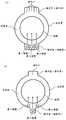
图1是本发明实施方式中适用的基板处理装置的立式处理炉的概要结构图,是以纵剖视图来表示处理炉部分的图。FIG. 1 is a schematic configuration diagram of a vertical processing furnace of a substrate processing apparatus to which an embodiment of the present invention is applied, and is a longitudinal cross-sectional view showing a portion of the processing furnace.
图2是本发明实施方式中适用的基板处理装置的立式处理炉的局部概要结构图,是以图1的A-A线剖视图来表示处理炉的一部分的图。2 is a partial schematic configuration diagram of a vertical processing furnace of the substrate processing apparatus to which the embodiment of the present invention is applied, and is a diagram showing a part of the processing furnace as a cross-sectional view taken along the line A-A in FIG. 1 .
图3是本发明的实施方式中适用的基板处理装置的控制器的概要结构图,是以框图来表示控制器的控制系统的图。3 is a schematic configuration diagram of a controller of the substrate processing apparatus to which the embodiment of the present invention is applied, and is a block diagram showing a control system of the controller.
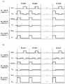
图4的(a)、(b)分别为表示本发明的一个实施方式的成膜时序的图。(a) and (b) of FIGS. 4A and 4B are diagrams respectively showing the film-forming sequence according to one embodiment of the present invention.
图5的(a)、(b)分别为表示立式处理炉的变形例的横剖视图,是将反应管、缓冲室和喷嘴等局部地抽出表示的图。FIGS. 5( a ) and ( b ) are respectively transverse cross-sectional views showing modified examples of the vertical processing furnace, and are views showing partially extracted reaction tubes, buffer chambers, nozzles, and the like.
图6的(a)、(b)分别为表示在基板上形成的膜的基板面内膜厚分布的测定结果的图。(a) and (b) of FIGS. 6A and 6B are diagrams showing the measurement results of the film thickness distribution in the substrate plane of the film formed on the substrate, respectively.
图7的(a)、(b)分布为表示在基板上形成的膜的基板面内膜厚分布的测定结果的图。(a) and (b) distributions of FIG. 7 are diagrams showing the measurement results of the film thickness distribution in the substrate plane of the film formed on the substrate.
具体实施方式Detailed ways
<本发明的一个实施方式><One embodiment of the present invention>
以下参照图1~图3、图4的(a)和图4的(b)对本发明的一个实施方式进行说明。Hereinafter, one embodiment of the present invention will be described with reference to FIGS. 1 to 3 , and FIGS. 4( a ) and 4 ( b ).
(1)基板处理装置的结构(1) Structure of a substrate processing apparatus
如图1所示,处理炉202具有作为加热机构(温度调整部)的加热器207。加热器207呈圆筒形状,且被保持板支撑而垂直地安装设置。加热器207也作为利用热使气体活化(进行激励)的活化机构(激励部)发挥功能。As shown in FIG. 1 , the
在加热器207的内侧与加热器207呈同心圆状配设有反应管203。反应管203例如由石英(SiO2)或者碳化硅(SiC)等耐热性材料构成,并形成为上端封闭且下端开口的圆筒形状。在反应管203的下方与反应管203呈同心圆状配设有集管209。集管209例如由不锈钢(SUS)等金属材料构成,并形成为上端和下端开口的圆筒形状。集管209的上端部与反应管203的下端部卡合,并且构成为对反应管203进行支撑。在集管209与反应管203之间设有作为密封部件的O型环220a。反应管203与加热器207同样地垂直安装设置。主要由反应管203和集管209构成处理容器(反应容器)。在处理容器的筒中空部形成处理室201。处理室201构成为能够收纳作为基板的晶圆200。在该处理室201内对晶圆200进行处理。Inside the
在处理室201内,作为第一~第三供给部的喷嘴249a~249c分别以贯通集管209的侧壁的方式设置。喷嘴249a~249c分别与气体供给管232a~232c连接。喷嘴249a~249c是各不相同的喷嘴,喷嘴249a、249c各自与喷嘴249b相邻设置。In the
在气体供给管232a~232c上从气流的上游侧起依次分别设有作为流量控制器(流量控制部)的质量流量控制器(MFC)241a~241c和作为开闭阀的阀门243a~243c。相对于气体供给管232a~232c的阀门243a~243c而言在下游侧分别连接有气体供给管232d~232f。在气体供给管232d~232f上从气流的上游侧起依次分别设有MFC241d~241f和阀门243d~243f。Mass flow controllers (MFCs) 241a to 241c serving as flow controllers (flow rate controllers) and
如图2所示,喷嘴249a~249c在反应管203的内壁与晶圆200之间的俯视呈圆环状的空间分别设置为从反应管203的内壁的下部沿着上部向晶圆200的配置方向上方立起。即,喷嘴249a~249c在供晶圆200排列的晶圆排列区域的侧方的水平地围绕晶圆排列区域的区域,沿着晶圆排列区域设置。俯视下,喷嘴249b配置为与后述的排气口231a夹着搬入处理室201内的晶圆200的中心在一直线上对置。喷嘴249a、249c配置为沿着反应管203的内壁(晶圆200的外周部)从两侧夹着通过喷嘴249b和排气口231a的中心的直线L。直线L也是通过喷嘴249b和晶圆200的中心的直线。也可以说,喷嘴249c与喷嘴249a夹着直线L设置于相反侧。喷嘴249a、249c以直线L为对称轴呈线对称进行配置。在喷嘴249a~249c的侧面分别设有供给气体的气体供给孔250a~250c。气体供给孔250a~250c分别以俯视下与排气口231a对置(面对)的方式开口,并且能够朝向晶圆200供给气体。气体供给孔250a~250c从反应管203的下部到上部设有多个。As shown in FIG. 2 , the
作为第一处理气体(原料气体),例如可将包含作为构成想要在基板上形成的膜的主元素(预定元素)的硅(Si)的气体即硅烷类气体从气体供给管232b经由MFC241b、阀门243b、喷嘴249b向处理室201内供给。作为硅烷类气体,例如可以采用包含氯(Cl)、氟(F)、溴(Br)、碘(I)等卤族元素的卤硅烷类气体。作为卤硅烷类气体,例如可以采用包含Si和Cl的氯硅烷类气体,例如可以采用六氯二硅烷(Si2Cl6、简称为HCDS)气体。As the first process gas (raw material gas), for example, a gas containing silicon (Si) as the main element (predetermined element) constituting a film to be formed on the substrate, that is, a silane-based gas can be passed from the
作为分子结构与上述的第一处理气体不同的第二处理气体(反应气体),例如可将作为氮化剂的含(N)气体从气体供给管232a、232c分别经由MFC241a、241c、阀门243a、243c、喷嘴249a、249c向处理室201内供给。作为含N气体,例如可以采用由氮(N)和氢(H)两种元素构成的气体即氮化氢类气体。作为氮化氢类气体,例如可以采用氨气(NH3)。As the second processing gas (reactive gas) having a different molecular structure from the above-described first processing gas, for example, a gas containing (N) as a nitriding agent can be passed from the
作为惰性气体,例如可将氮气(N2)从气体供给管232d~232f分别经由MFC241d~241f、阀门243d~243f、气体供给管232a~232c、喷嘴249a~249c向处理室201内供给。N2气体作为吹扫气体、载气、稀释气体等发挥作用,此外还作为对在晶圆200上形成的膜的晶圆面内膜厚分布进行控制的膜厚分布控制气体发挥作用。As the inert gas, for example, nitrogen gas (N2 ) can be supplied into the
主要由气体供给管232d、MFC241d、阀门243d构成从喷嘴249a供给惰性气体的第一供给系统。主要由气体供给管232b、MFC241b、阀门243b构成从喷嘴249b供给第一处理气体的第二供给系统。主要由气体供给管232f、MFC241f、阀门243f构成从喷嘴249c供给惰性气体的第三供给系统。主要由气体供给管232a、MFC241a、阀门243a和气体供给管232c、MFC241c、阀门243c中的至少一方构成从喷嘴249a、249c中的至少一方供给第二处理气体的第四供给系统。The first supply system for supplying the inert gas from the
上述的各种供给系统中的任一个、或者全部的供给系统也可以构成为由阀门243a~243f、MFC241a~241f等集成的集成型供给系统248。集成型供给系统248与各气体供给管232a~232f连接,并构成为通过后述的控制器121来控制:各种气体向气体供给管232a~232f内的供给动作、即阀门243a~243f的开闭动作;通过MFC241a~241f进行的流量调整动作等。集成型供给系统248构成为一体型或者分割型的集成单元,且能够以集成单元为单位相对于气体供给管232a~232f等进行装卸,并构成为能够以集成单元为单位进行集成型供给系统248的维护、交换、增设等。Any or all of the above-mentioned various supply systems may be configured as an
在反应管203的侧壁下方设有对处理室201内的环境气体进行排气的排气口231a。如图2所示,排气口231a设置于俯视下隔着晶圆200与喷嘴249a~249c(气体供给孔250a~250c)对置(面对)的位置。排气口231a也可以从反应管203的侧壁的下部沿着上部、即沿着晶圆排列区域设置。排气口231a与排气管231连接。排气管231经由作为对处理室201内的压力进行检测的压力检测器(压力检测部)的压力传感器245和作为压力调整器(压力调整部)的APC(Auto Pressure Controller:自动压力控制器)阀门244与作为真空排气装置的真空泵246连接。APC阀门244构成为:能够在使真空泵246动作的状态下开闭阀,从而对处理室201内进行真空排气和停止真空排气,此外,能够在使真空泵246动作的状态下,基于通过压力传感器245检测的压力信息来调节阀开度,从而对处理室201内的压力进行调整。主要由排气管231、APC阀门244、压力传感器245构成排气系统。也可以认为真空泵246包含于排气系统。An
在集管209的下方设有密封盖219,该密封盖219作为炉口盖体能够将集管209的下端开口气密地封闭。密封盖219例如由SUS等金属材料构成并形成为圆盘状。在密封盖219的上表面设有与集管209的下端抵接的作为密封部件的O型环220b。在密封盖219的下方设置有使后述的晶舟217旋转的旋转机构267。旋转机构267的旋转轴255贯通密封盖219并与晶舟217连接。旋转机构267构成为通过使晶舟217旋转而使晶圆200旋转。密封盖219构成为能够利用在反应管203外部设置的作为升降机构的晶舟升降机115在垂直方向上升降。晶舟升降机115构成为输送装置(输送机构),能够通过使密封盖219升降而将晶圆200向处理室201内外搬入和搬出(输送)。在集管209的下方设有作为炉口盖体的闸门219s,该闸门219s能够在使密封盖219下降并将晶舟217从处理室201内搬出的状态下将集管209的下端开口气密地封闭。闸门219s例如由SUS等金属材料构成并形成为圆盘状。在闸门219s的上表面设有与集管209的下端抵接的作为密封部件的O型环220c。闸门219s的开闭动作(升降动作、转动动作等)通过闸门开闭机构115s进行控制。A sealing
作为基板支撑件的晶舟217构成为将多张、例如是25~200张的晶圆200以水平姿态并且以彼此中心一致的状态在垂直方向上整齐排列并以多层方式支撑,即隔开间隔排列。晶舟217例如由石英、SiC等耐热性材料构成。在晶舟217的下部以多层方式支撑有:例如由石英、SiC等耐热性材料构成的隔热板218。The
在反应管203内设有作为温度检测器的温度传感器263。基于通过温度传感器263检出的温度信息来调整加热器207的通电状态,从而使得处理室201内的温度成为所需的温度分布。温度传感器263沿着反应管203的内壁设置。A
如图3所示,控制部(控制单元)即控制器121由计算机构成,该计算机具备:CPU(Central Processing Unit:中央处理单元)121a、RAM(Random Access Memory:随机存取存储器)121b、存储装置121c、I/O端口121d。RAM121b、存储装置121c、I/O端口121d构成为能够经由内部总线121e与CPU121a进行数据交换。控制器121例如与构成为触控面板等的输入输出装置122连接。As shown in FIG. 3 , the
存储装置121c例如由闪存、HDD(Hard Disk Drive:硬盘驱动器)等构成。在存储装置121c内以可读取的方式存储有:对基板处理装置的动作进行控制的控制程序、记载有后述的基板处理的步骤、条件等的制程处方等。制程处方以能够使控制器121执行后述的基板处理中的各步骤、获得预定的结果的方式组合而成并作为程序发挥功能。以下也简单地将制程处方、控制程序等统称为程序。另外,也将制程处方简称为处方。在本说明书中,“程序”这一用语的含义包括:仅指处方单体、仅指控制程序单体、或者是指这两方。RAM121b构成为存储区域(工作区域),可将通过CPU121a读取的程序、数据等暂时地保持。The
I/O端口121d与上述的MFC241a~241f、阀门243a~243f、压力传感器245、APC阀门244、真空泵246、温度传感器263、加热器207、旋转机构267、晶舟升降机115、闸门开闭机构115s等连接。The I/
CPU121a构成为从存储装置121c读取控制程序并执行,并且按照从输入输出装置122输入的操作命令等而从存储装置121c读取处方。CPU121a构成为能够按照读取的处方的内容来对以下各项进行控制,即:MFC241a~241f对各种气体的流量调整动作、阀门243a~243f的开闭动作、APC阀门244的开闭动作和基于压力传感器245的APC阀门244的压力调整动作、真空泵246的启动和停止、基于温度传感器263的加热器207的温度调整动作、通过旋转机构267进行的晶舟217的旋转和旋转速度调节动作、通过晶舟升降机115进行的晶舟217的升降动作、通过闸门开闭机构115s进行的闸门219s的开闭动作等。The
控制器121可以通过将外部存储装置123中所存储的上述的程序安装于计算机而构成。外部存储装置123例如包括:HDD等磁盘、CD等光盘、MO等光磁盘、USB存储器等半导体存储器等。存储装置121c、外部存储装置123构成为计算机可读取的存储介质。以下也简单地将它们统称为存储介质。在本说明书中,“存储介质”这一用语的含义包括:仅指存储装置121c单体、仅指外部存储装置123单体、或者是指这两方。此外,程序向计算机的提供也可以不使用外部存储装置123,而是利用互联网、专用线路等通信方式来进行。The
(2)基板处理工序(2) Substrate processing step
作为半导体装置的制造工艺的一工序,参照图4的(a)、图4的(b)对使用上述的基板处理装置在基板上形成膜的基板处理时序例、即成膜时序例进行说明。在以下的说明中,通过控制器121对构成基板处理装置的各部的动作进行控制。4( a ) and FIG. 4( b ), an example of a substrate processing sequence for forming a film on a substrate using the above-described substrate processing apparatus, that is, an example of a film formation sequence, will be described as a step of the manufacturing process of the semiconductor device. In the following description, the
在本实施方式的成膜时序中,执行如下步骤,即:In the film formation sequence of this embodiment, the following steps are performed, namely:
在处理室201内准备作为基板的晶圆200的步骤;以及the step of preparing the
相对于处理室201内的晶圆200而言,从作为第一供给部的喷嘴249a供给作为惰性气体的N2气体、从作为第二供给部的喷嘴249b供给作为第一处理气体的HCDS气体、从与喷嘴249a夹着通过喷嘴249b和晶圆200的中心的直线L设置于相反侧的作为第三供给部的喷嘴249c供给作为惰性气体的N2气体,在晶圆200上形成膜的步骤。With respect to the
在上述的形成膜的步骤中,对从喷嘴249a供给的N2气体的流量、与从喷嘴249c供给的N2气体的流量的平衡进行控制,从而调整膜的晶圆面内膜厚分布(以下也简称为面内膜厚分布)。In the above-described film forming step, the balance of the flow rate of the N2 gas supplied from the
在图4的(a)和图4的(b)所示的成膜时序中,作为一例示出了如下情况:In the film formation sequences shown in FIG. 4( a ) and FIG. 4( b ), the following cases are shown as an example:
在上述的形成膜的步骤中,通过将非同时地执行如下步骤的循环执行预定次数(n次、n为1以上的整数),从而在晶圆200上作为膜而形成包含Si和N的膜、即硅氮化膜(SiN膜),其中,In the above-mentioned step of forming a film, a film containing Si and N is formed as a film on the
所述循环中执行的步骤为:The steps performed in the loop are:
相对于处理室201内的晶圆200而言,从喷嘴249a供给N2气体、从喷嘴249b供给HCDS气体、从喷嘴249c供给N2气体的步骤1;以及With respect to the
向处理室201内的晶圆200供给作为第二处理气体的NH3气体的步骤2。
此外,在图4的(a)所示的成膜时序中,作为流量平衡控制的一例,示出了如下的情况:在上述的步骤1中,从喷嘴249b向晶圆200供给HCDS气体时,使从喷嘴249a供给的N2气体的流量、与从喷嘴249c供给的N2气体的流量相同。In addition, in the film formation sequence shown in FIG. 4( a ), as an example of the flow rate balance control, in the above-mentioned step 1, when the HCDS gas is supplied from the
另外,在图4的(b)所示的成膜时序中,作为流量平衡控制的另一例,示出了如下的情况:在上述的步骤1中,从喷嘴249b向晶圆200供给HCDS气体时,使从喷嘴249a供给的N2气体的流量、与从喷嘴249c供给するN2气体的流量不同。In addition, in the film formation sequence shown in FIG. 4( b ), as another example of the flow rate balance control, the case where the HCDS gas is supplied to the
在以下的说明中,作为一例,对作为晶圆200使用没有在表面形成凹凸结构的表面积较小的裸基板、即裸晶圆,并通过上述的成膜时序和流量控制来调整SiN膜的面内膜厚分布的例子进行说明。在本说明书中,也将在晶圆200的中央部最厚并随着接近外周部(周缘部)而逐渐变薄的膜的面内膜厚分布称为中央凸分布。另外,将在晶圆200的中央部最薄并随着接近外周部而逐渐变厚的膜的面内膜厚分布称为中央凹分布。另外,也将从晶圆200的中央部到外周部而膜厚变化较少的平坦的膜的面内膜厚分布称为扁平分布。如果能够在裸晶圆上形成具有中央凸分布的膜,则能够在表面形成有微小的凹凸结构的表面积较大的图案晶圆(产品晶圆)上形成具有扁平分布的膜。In the following description, as an example, as the
在本说明书中,有时为了方便也将图4的(a)、图4的(b)所示的成膜时序以如下方式表示。在以下对变形例等的说明中也使用同样的标记。In this specification, the film-forming sequence shown in FIGS. 4( a ) and 4 ( b ) may be expressed as follows for convenience. The same symbols are used in the following description of the modification and the like.

在本说明书中,“晶圆”这一用语的含义包括:指晶圆本身、或者是指晶圆与在其表面形成的预定的层、膜的层叠体。在本说明书中,“晶圆的表面”这一用语的含义包括:指晶圆本身的表面、或者是指在晶圆上形成的预定的层等的表面。在本说明书中,“在晶圆上形成预定的层”这一记载的含义包括:指在晶圆本身的表面上直接形成预定的层、或者是指在形成于晶圆上的层等之上形成预定的层。在本说明书中,“基板”这一用语的含义与“晶圆”这一用语的含义相同。In this specification, the term "wafer" means a wafer itself, or a laminate of a wafer and a predetermined layer or film formed on the surface thereof. In this specification, the term "surface of a wafer" means the surface of the wafer itself, or the surface of a predetermined layer or the like formed on the wafer. In this specification, the meaning of the description "to form a predetermined layer on a wafer" includes: directly forming a predetermined layer on the surface of the wafer itself, or referring to a layer formed on the wafer, etc. A predetermined layer is formed. In this specification, the term "substrate" has the same meaning as the term "wafer".
(晶圆装填和晶舟装载)(wafer loading and boat loading)
当将多张晶圆200向晶舟217装填(晶圆装填)时,则利用闸门开闭机构115s使闸门219s移动,使集管209的下端开口开放(闸门开放)。之后,如图1所示,对多张晶圆200进行支撑的晶舟217被晶舟升降机115提升并向处理室201内搬入(晶舟装载)。在该状态下,密封盖219成为经由O型环220b将集管209的下端密封的状态。通过这些动作在处理室201内准备晶圆200。When a plurality of
(压力调整和温度调整)(pressure adjustment and temperature adjustment)
在处理室201内准备了晶圆200之后,为了使处理室201内、即晶圆200存在的空间成为所需的压力(真空度)而利用真空泵246进行真空排气(减压排气)。此时,通过压力传感器245来测定处理室201内的压力,并基于该测定的压力信息来对APC阀门244进行反馈控制。另外,为了使处理室201内的晶圆200成为所需的成膜温度而利用加热器207进行加热。此时,为了使处理室201内成为所需的温度分布而基于温度传感器263检出的温度信息来对加热器207的通电状态进行反馈控制。另外,利用旋转机构267使晶圆200开始旋转。处理室201内的排气、晶圆200的加热和旋转都至少在对晶圆200的处理结束之前持续进行。After the
(成膜步骤)(film formation step)
之后,依次执行后续的步骤1、2。After that, the
[步骤1][step 1]
在该步骤中,相对于处理室201内的晶圆200而言,从喷嘴249a供给N2气体、从喷嘴249b供给HCDS气体、从喷嘴249c供给N2气体。In this step, the N2 gas is supplied from the
具体而言,是打开阀门243b向气体供给管232b内流通HCDS气体。HCDS气体通过MFC241b进行流量调整,经由喷嘴249b向处理室201内供给,并从排气口231a进行排气。此时,向晶圆200供给HCDS气体。另外,此时打开阀门243d、243f,分别向气体供给管232d、232f内流通N2气体。N2气体分别通过MFC241d、241f进行流量调整,且分别经由气体供给管232a、232c、喷嘴249a、249c向处理室201内供给,并从排气口231a进行排气。此时,向晶圆200供给N2气体。N2气体在处理室201内与HCDS气体混合。此时,也可以打开阀门243e,向气体供给管232e内流通N2气体。N2气体通过MFC241e进行流量调整,且在气体供给管232b内、喷嘴249b内与HCDS气体混合,向处理室201内供给,并从排气口231a进行排气。Specifically, the
通过向晶圆200供给HCDS气体,从而在晶圆200的表面上作为第一层而形成包含Cl的含Si层。包含Cl的含Si层通过在晶圆200的表面上以物理方式吸附HCDS、或者以化学方式对HCDS的一部分发生分解而产生的物质进行吸附、或者通过HCDS发生热解而沉积Si等方式来形成。即,包含Cl的含Si层可以是HCDS或者HCDS的一部分发生分解而产生的物质的吸附层(物理吸附层或者化学吸附层),也可以是包含Cl的Si的沉积层(Si层)。以下也将包含Cl的含Si层简称为含Si层。By supplying the HCDS gas to the
在本步骤中,从喷嘴249b向晶圆200供给HCDS气体时,分别经由喷嘴249a、249c向处理室201内供给N2气体。此时,对从喷嘴249a供给的N2气体的流量、与从喷嘴249c供给的N2气体的流量的平衡进行控制。由此能够如以下说明的那样自由地对在晶圆200上形成的第一层的晶圆面内厚度分布(以下也简称为面内厚度分布)进行调整。In this step, when the HCDS gas is supplied from the
例如是如图4的(a)所示那样,在从喷嘴249b向晶圆200供给HCDS气体时,使从喷嘴249a供给的N2气体的流量、与从喷嘴249c供给的N2气体的流量相同。通过这样对供给HCDS气体时的N2气体的流量平衡进行控制,从而能够分别向如下的方向进行控制,即:使向晶圆200的中央部供给的HCDS气体的浓度即分压(供给量)升高(增大)的方向;以及使向晶圆200的外周部供给的HCDS气体的浓度即分压(供给量)降低(减小)的方向。结果是,能够使在构成为裸晶圆的晶圆200上形成的第一层的面内厚度分布成为中央凸分布。For example, as shown in FIG. 4( a ), when the HCDS gas is supplied from the
此外,在使从喷嘴249a供给的N2气体的流量、与从喷嘴249c供给的N2气体的流量相同的情况下,可以如图4的(a)所示那样,使各流量比从喷嘴249b供给的HCDS气体的流量大。通过这样对供给HCDS气体时的N2气体的流量平衡进行控制,从而能够切实地使在构成为裸晶圆的晶圆200上形成的第一层的面内厚度分布成为中央凸分布。In addition, when the flow rate of the N2 gas supplied from the
另外,例如是如图4的(b)所示那样,在从喷嘴249b向晶圆200供给HCDS气体时,使从喷嘴249a供给的N2气体的流量、与从喷嘴249c供给的N2气体的流量不同。即,使从喷嘴249a供给的N2气体的流量和从喷嘴249c供给的N2气体的流量的其中一方的流量比另一方的流量大。图4的(b)示出了使从喷嘴249c供给的N2气体的流量比从喷嘴249a供给的N2气体的流量大的例子。通过这样对供给HCDS气体时的N2气体的流量平衡进行控制,从而能够分别向如下的方向进行控制,即:使向晶圆200的中央部供给的HCDS气体的浓度即分压(供给量)降低(减小)的方向;以及使向晶圆200的外周部供给的HCDS气体的浓度即分压(供给量)升高(增大)的方向。结果是,能够使在构成为裸晶圆的晶圆200上形成的第一层的面内厚度分布从中央凸分布接近扁平分布、进而接近中央凹分布。In addition, as shown in FIG. 4(b), for example, when supplying the HCDS gas from the
此外,在使从喷嘴249c供给的N2气体的流量比从喷嘴249a供给的N2气体的流量大的情况下,可以使从喷嘴249c供给的N2气体的流量比从喷嘴249b供给的HCDS气体的流量大。通过这样对供给HCDS气体时的N2气体的流量平衡进行控制,从而能够切实地使在构成为裸晶圆的晶圆200上形成的第一层的面内厚度分布从中央凸分布接近扁平分布、进而接近中央凹分布。In addition, when the flow rate of the N2 gas supplied from the
另外,在使从喷嘴249c供给的N2气体的流量比从喷嘴249a供给的N2气体的流量大的情况下,可以使从喷嘴249a供给的N2气体的流量比从喷嘴249b供给的HCDS气体的流量小。通过这样对供给HCDS气体时的N2气体的流量平衡进行控制,从而能够切实地使在构成为裸晶圆的晶圆200上形成的第一层的面内厚度分布从中央凸分布接近扁平分布、进而接近中央凹分布。In addition, when the flow rate of the N2 gas supplied from the
另外,在使从喷嘴249c供给的N2气体的流量比从喷嘴249a供给的N2气体的流量大的情况下,可以是如图4的(b)所示那样,使从喷嘴249c供给的N2气体的流量比从喷嘴249b供给的HCDS气体的流量大,并且使从喷嘴249a供给的N2气体的流量比从喷嘴249b供给的HCDS气体的流量小。通过这样对供给HCDS气体时的N2气体的流量平衡进行控制,从而能够更加切实地使在构成为裸晶圆的晶圆200上形成的第一层的面内厚度分布从中央凸分布接近扁平分布、进而接近中央凹分布。In addition, when the flow rate of the N2 gas supplied from the
另外,在使从喷嘴249c供给的N2气体的流量比从喷嘴249a供给的N2气体的流量大的情况下,可以使从喷嘴249a供给的N2气体的流量为零。即可以不实施N2气体从喷嘴249a的供给。通过这样对供给HCDS气体时的N2气体的流量平衡进行控制,从而能够切实地使在构成为裸晶圆的晶圆200上形成的第一层的面内厚度分布从中央凸分布接近扁平分布、进而接近中央凹分布。In addition, when the flow rate of the N2 gas supplied from the
另外,在使从喷嘴249c供给的N2气体的流量比从喷嘴249a供给的N2气体的流量大的情况下,可以使从喷嘴249c供给的N2气体的流量比从喷嘴249b供给的HCDS气体的流量大,并且使从喷嘴249a供给的N2气体的流量为零。通过这样对供给HCDS时的N2气体的流量平衡进行控制,从而能够更加切实地使在构成为裸晶圆的晶圆200上形成的第一层的面内厚度分布从中央凸分布接近扁平分布、进而接近中央凹分布。In addition, when the flow rate of the N2 gas supplied from the
当在晶圆200上形成了具有所需的面内厚度分布的第一层之后,关闭阀门243b,停止向处理室201内供给HCDS气体。并且,对处理室201内进行真空排气,将处理室201内残留的气体等从处理室201内排除。此时,打开阀门243d~243f,经由喷嘴249a~249c向处理室201内供给N2气体。从喷嘴249a~249c供给的N2气体作为吹扫气体发挥作用,由此对处理室201内进行吹扫(吹扫步骤)。After the first layer having the desired in-plane thickness distribution is formed on the
[步骤2][Step 2]
在步骤1结束后,向处理室201内的晶圆200、即在晶圆200上形成的第一层供给NH3气体。After step 1 is completed, NH3 gas is supplied to the
具体而言,是打开阀门243a向气体供给管232a内流通NH3气体。NH3气体通过MFC241a进行流量调整,经由喷嘴249a向处理室201内供给,并通过排气口231a进行排气。此时,向晶圆200供给NH3气体。另外,此时打开阀门243e、243f,分别经由喷嘴249b、249c向处理室201内供给N2气体。也可以不实施N2气体从喷嘴249b、249c的供给。Specifically, the
通过向晶圆200供给NH3气体,从而使在晶圆200上形成的第一层的至少一部分氮化(改性)。通过使第一层改性,从而在晶圆200上形成包含Si和N的第二层即SiN层。在形成第二层时,第一层所含的Cl等杂质在利用NH3气体进行的第一层的改性反应的过程中,构成至少含Cl的气体状物质并从处理室201内排出。由此,第二层成为与第一层相比Cl等杂质较少的层。By supplying NH3 gas to the
当在晶圆200上形成了第二层之后,关闭阀门243a,停止向处理室201内供给NH3气体。并且,按照与步骤1的吹扫步骤同样的处理步骤、处理条件,将处理室201内残留的气体等从处理室201内排除。After the second layer is formed on the
[实施预定次数][implementation scheduled times]
通过将使上述的步骤1、2交替地、即非同步地进行的循环执行一次以上(n次),从而能够在晶圆200上形成预定组成和预定膜厚的SiN膜。上述的循环优选重复进行多次。即优选,使在进行一次上述的循环时形成的第二层的厚度比所需的膜厚薄,并在通过层叠第二层而形成的SiN膜的膜厚达到所需的膜厚之前,重复多次上述的循环。A SiN film of a predetermined composition and a predetermined thickness can be formed on the
根据本实施方式,通过对在步骤1中形成的第一层的面内厚度分布进行调整,从而能够自由地对在晶圆200上形成的SiN膜的面内膜厚分布进行调整。例如,通过使在步骤1中形成的第一层的面内厚度分布为中央凸分布,从而能够使在晶圆200上形成的SiN膜的面内膜厚分布为中央凸分布。另外,例如通过使在步骤1中形成的第一层的面内厚度分布为扁平分布或中央凹分布,从而能够使在晶圆200上形成的SiN膜的面内膜厚分布为扁平分布或中央凹分布。According to the present embodiment, by adjusting the in-plane thickness distribution of the first layer formed in Step 1, the in-plane thickness distribution of the SiN film formed on the
作为步骤1中的处理条件,例示如下。The processing conditions in Step 1 are exemplified as follows.
HCDS气体供给流量:100~2000sccmHCDS gas supply flow: 100~2000sccm
N2气体供给流量(气体供给管232a):0~10000sccmN2 gas supply flow rate (
N2气体供给流量(气体供给管232c):0~10000sccmN2 gas supply flow rate (
气体供给时间:1~120秒、优选1~60秒Gas supply time: 1 to 120 seconds, preferably 1 to 60 seconds
处理温度:250~700℃、优选300~650℃、更优选350~600℃Treatment temperature: 250 to 700°C, preferably 300 to 650°C, more preferably 350 to 600°C
处理压力:1~2666Pa、优选67~1333PaProcessing pressure: 1~2666Pa, preferably 67~1333Pa
此外,本说明书中的如“250~700℃”这样的数值范围的标记表示包含下限值和上限值。因此,“250~700℃”是指“250℃以上且700℃以下”。对于其它的数值范围而言也同样。In addition, the notation of the numerical range like "250-700 degreeC" in this specification shows that a lower limit and an upper limit are included. Therefore, "250-700 degreeC" means "250 degreeC or more and 700 degrees C or less". The same applies to other numerical ranges.
作为步骤2中的处理条件,例示如下。The processing conditions in
NH3气体供给流量:100~10000sccmNH3 gas supply flow: 100~10000sccm
N2气体供给流量(各气体供给管):0~10000sccmN2 gas supply flow rate (each gas supply pipe): 0~10000sccm
其它的处理条件可以与步骤1中的处理条件相同。Other processing conditions may be the same as those in step 1.
作为第一处理气体,除了HCDS气体之外,也可以适用:一氯硅烷(SiH3Cl、简称为MCS)气体、二氯硅烷(SiH2Cl2、简称为DCS)气体、三氯硅烷(SiHCl3、简称为TCS)气体、四氯硅烷(SiCl4、简称为STC)气体、八氯三硅烷(Si3Cl8、简称为OCTS)气体等氯硅烷类气体。另外,也可以取代这些气体而适用:四氟硅烷(SiF4)气体、四溴硅烷(SiBr4)气体、四碘硅烷(SiI4)气体等。即可以取代氯硅烷类气体而适用:氟硅烷类气体、溴硅烷类气体、碘硅烷类气体等卤硅烷类气体。As the first process gas, in addition to HCDS gas, monochlorosilane (SiH3 Cl, abbreviated as MCS) gas, dichlorosilane (SiH2 Cl2 , abbreviated as DCS) gas, trichlorosilane (SiHCl, abbreviated as DCS) gas can also be applied.3. Chlorosilane-based gases such as TCS gas, tetrachlorosilane (SiCl4 , STC for short) gas, octachlorotrisilane (Si3 Cl8 , OCTS for short) gas. In addition, instead of these gases, tetrafluorosilane (SiF4 ) gas, tetrabromosilane (SiBr4 ) gas, tetraiodosilane (SiI4 ) gas, and the like can be applied. That is, instead of chlorosilane-based gas, it can be applied to halosilane-based gas such as fluorosilane-based gas, bromosilane-based gas, and iodosilane-based gas.
作为第二处理气体,除了NH3气体之外,例如也可以采用二亚胺(N2H2)气体、联氨(N2H4)气体、N3H8气体等氮化氢类气体。As the second processing gas, in addition to NH3 gas, for example, hydrogen nitride-based gas such as diimine (N2 H2 ) gas, hydrazine (N2 H4 ) gas, and N3 H8 gas may be used.
作为惰性气体,除了N2气体之外,也可以采用Ar气体、He气体、Ne气体、Xe气体等稀有气体。As the inert gas, in addition to N2 gas, rare gases such as Ar gas, He gas, Ne gas, and Xe gas can also be used.
(后吹扫和大气压恢复)(Post purge and atmospheric pressure recovery)
在成膜步骤结束后,从喷嘴249a~249c分别将作为吹扫气体的N2气体向处理室201内供给,并从排气口231a进行排气。由此,对处理室201内进行吹扫,将处理室201内残留的气体、反应副产物从处理室201内除去(后吹扫)。之后,将处理室201内的环境气体置换为惰性气体(惰性气体置换),使处理室201内的压力恢复为常压(大气压恢复)。After the film formation step is completed, N2 gas as a purge gas is supplied into the
(晶舟卸载和晶圆卸除)(boat unloading and wafer unloading)
利用晶舟升降机115使密封盖219下降,使集管209的下端开口。并且将处理后的晶圆200以被晶舟217支撑的状态从集管209的下端向反应管203的外部搬出(晶舟卸载)。在晶舟卸载之后,使闸门219s移动,利用闸门219s并经由O型环220c将集管209的下端开口密封(闸门关闭)。处理后的晶圆200被搬出到反应管203的外部之后,通过晶舟217被取出(晶圆卸除)。The sealing
(3)本实施方式的效果(3) Effects of the present embodiment
根据本实施方式,可以获得如下所示的一个或者多个效果。According to the present embodiment, one or more of the following effects can be obtained.
(a)在步骤1中从喷嘴249b供给HCDS气体时,使从喷嘴249a供给的N2气体的流量、与从喷嘴249c供给的N2气体的流量相同,从而当在构成为裸晶圆的晶圆200上形成SiN膜时,能够实现使得该膜的面内膜厚分布成为中央凸分布的条件。(a) In step 1, when the HCDS gas is supplied from the
此外,在使从喷嘴249a供给的N2气体的流量、与从喷嘴249c供给的N2气体的流量相同的情况下,使各流量比从喷嘴249b供给的HCDS气体的流量大,从而能够切实地实现使得该膜的面内膜厚分布成为中央凸分布的条件。In addition, when the flow rate of the N2 gas supplied from the
(b)在步骤1中从喷嘴249b供给HCDS气体时,使从喷嘴249a供给的N2气体的流量、与从喷嘴249c供给的N2气体的流量不同,例如使从喷嘴249c供给的N2气体的流量比从喷嘴249a供给的N2气体的流量大,从而当在构成为裸晶圆的晶圆200上形成SiN膜时,能够实现使得该膜的面内膜厚分布成为中央凸分布与中央凹分布之间的任意分布的条件。(b) When the HCDS gas is supplied from the
此外,在使从喷嘴249a供给的N2气体的流量、与从喷嘴249c供给的N2气体的流量不同的情况下,使从喷嘴249c供给的N2气体的流量比从喷嘴249a供给的N2气体的流量大,并使从喷嘴249c供给的N2气体的流量比从喷嘴249b供给的HCDS气体的流量大,从而能够切实地实现使得SiN膜的面内膜厚分布成为中央凸分布与中央凹分布之间的任意分布的条件。In addition, when the flow rate of the N2 gas supplied from the
另外,在使从喷嘴249a供给的N2气体的流量、与从喷嘴249c供给的N2气体的流量不同的情况下,使从喷嘴249c供给的N2气体的流量比从喷嘴249a供给的N2气体的流量大,并使从喷嘴249a供给的N2气体的流量比从喷嘴249b供给的HCDS气体的流量小,从而能够切实地实现使得SiN膜的面内膜厚分布成为中央凸分布与中央凹分布之间的任意分布的条件。In addition, when the flow rate of the N2 gas supplied from the
另外,在使从喷嘴249a供给的N2气体的流量、与从喷嘴249c供给的N2气体的流量不同的情况下,使从喷嘴249c供给的N2气体的流量比从喷嘴249a供给的N2气体的流量大,使从喷嘴249c供给的N2气体的流量比从喷嘴249b供给的HCDS气体的流量大,并且使从喷嘴249a供给的N2气体的流量比从喷嘴249b供给的HCDS气体的流量小,从而能够更加切实地实现使得SiN膜的面内膜厚分布成为中央凸分布与中央凹分布之间的任意分布的条件。In addition, when the flow rate of the N2 gas supplied from the
另外,在使从喷嘴249a供给的N2气体的流量、与从喷嘴249c供给的N2气体的流量不同的情况下,使从喷嘴249c供给的N2气体的流量比从喷嘴249a供给的N2气体的流量大,并使从喷嘴249a供给的N2气体的流量为零,从而能够切实地实现使得SiN膜的面内膜厚分布成为中央凸分布与中央凹分布之间的任意分布的条件。In addition, when the flow rate of the N2 gas supplied from the
另外,在使从喷嘴249a供给的N2气体的流量、与从喷嘴249c供给的N2气体的流量不同的情况下,使从喷嘴249c供给的N2气体的流量比从喷嘴249a供给的N2气体的流量大,使从喷嘴249c供给的N2气体的流量比从喷嘴249b供给的HCDS气体的流量大,并且使从喷嘴249a供给的N2气体的流量为零,从而能够更加切实地实现使得SiN膜的面内膜厚分布成为中央凸分布与中央凹分布之间的任意分布的条件。In addition, when the flow rate of the N2 gas supplied from the
(c)如上所述,根据本实施方式,在步骤1中从喷嘴249b供给HCDS气体时,对从喷嘴249a供给的N2气体的流量、与从喷嘴249c供给的N2气体的流量的平衡进行控制,从而能够自由地对在晶圆200上形成的SiN膜的面内膜厚分布进行调整。如果能够在裸晶圆上形成具有中央凸分布的膜,则能够在表面形成有微小的凹凸结构的表面积较大的图案晶圆上形成具有扁平分布的膜。(c) As described above, according to the present embodiment, when the HCDS gas is supplied from the
此外,在晶圆200上形成的膜的面内膜厚分布与晶圆200的表面积有关,其原因被认为与所谓的负载效应有关。在如本实施方式的基板处理装置这样从晶圆200的外周部侧朝向中央部侧流通HCDS气体的情况下,成膜对象的晶圆200的表面积越大,则HCDS气体在晶圆200的外周部的消耗量就越多而难以到达晶圆200的中央部。其结果是,在晶圆200上形成的膜的面内膜厚分布会成为中央凹分布。根据本实施方式,即使在作为晶圆200而采用表面积较大的图案晶圆的情况下,也能够自由地进行控制而将在晶圆200上形成的膜的面内膜厚分布从中央凹分布矫正为扁平分布、进而矫正为中央凸分布等。In addition, the in-plane film thickness distribution of the film formed on the
(d)至少将喷嘴249b并优选将喷嘴249a~249c分别配置为至少俯视下与排气口231a对置,从而能够提高在晶圆200上形成的SiN膜的面内膜厚分布的控制性。另外,将喷嘴249a、249c配置为以直线L为对称轴呈线对称,从而能够进一步提高在晶圆200上形成的SiN膜的面内膜厚分布的控制性。(d) By arranging at least the
(e)使用HCDS气体以外的第一处理气体、使用NH3气体以外的第二处理气体、使用N2气体以外的惰性气体的情况下,也同样能够取得上述的效果。(e) In the case of using a first processing gas other than HCDS gas, using a second processing gas other than NH3 gas, and using an inert gas other than N2 gas, the above-described effects can be obtained similarly.
(4)变形例(4) Modifications
本实施方式的成膜步骤不限于图4的(a)、图4的(b)所示的方案,可以如以下所示的变形例那样进行变更。这些变形例可以任意地组合。在没有特别说明的情况下,各变形例的各步骤的处理步骤、处理条件可以与上述的基板处理时序的各步骤的处理步骤、处理条件相同。The film-forming step of the present embodiment is not limited to those shown in FIGS. 4( a ) and 4 ( b ), and can be changed as in the following modifications. These modifications can be combined arbitrarily. Unless otherwise specified, the processing steps and processing conditions of each step of each modification may be the same as the processing steps and processing conditions of each step of the above-described substrate processing sequence.
(变形例1)(Variation 1)
在步骤1中,使从喷嘴249a供给的N2气体的流量、与从喷嘴249c供给的N2气体的流量不同时,可以使从喷嘴249a供给的N2气体的流量比从喷嘴249c供给的N2气体的流量大。在本变形例中,也能够与图4的(b)所示的成膜时序同样地,使在构成为裸晶圆的晶圆200上形成的SiN膜的面内膜厚分布成为中央凸分布与中央凹分布之间的任意分布。In step 1, when the flow rate of the N2 gas supplied from the
(变形例2)(Variation 2)
在步骤2中,可以相对于处理室201内的晶圆200而言,从喷嘴249a供给N2气体、从喷嘴249b供给NH3气体、从喷嘴249c供给N2气体。并且,在从喷嘴249b向晶圆200供给NH3气体时,可以对从喷嘴249a供给的N2气体的流量、与从喷嘴249c供给的N2气体的流量的平衡进行控制。由此,能够通过执行步骤2来对在晶圆200上形成的第二层的晶圆面内组成分布、即通过执行成膜步骤而在晶圆200上形成的SiN膜的晶圆面内组成分布进行控制。In
(变形例3)(Variation 3)
作为第一处理气体,除了卤硅烷类气体之外,也可以适用:甲硅烷(SiH4、简称为MS)气体、乙硅烷(Si2H6、简称为DS)气体等氢化硅气体、三(二甲基氨基)硅烷(Si[N(CH3)2]3H、简称为3DMAS)气体、双(二乙基氨基)硅烷(Si[N(C2H5)2]2H2、简称为BDEAS)气体等氨基硅烷类气体。As the first process gas, in addition to halosilane-based gases, silicon hydride gases such as monosilane (SiH4 , abbreviated as MS) gas, disilane (Si2 H6 , abbreviated as DS) gas, tris( Dimethylamino)silane (Si[N(CH3 )2 ]3H , abbreviated as 3DMAS) gas, bis(diethylamino)silane (Si[N(C2H5)2 ]2H2 , abbreviated as It is aminosilane-based gas such as BDEAS) gas.
另外,作为第二处理气体,例如也可以适用:三乙胺((C2H5)3N、简称为TEA)气体等胺类气体、氧气(O2)、水蒸气(H2O气体)、臭氧(O3)气体、进行了等离子体激励的O2气体(O2*)、O2气体+氢气(H2)等含氧(O)气体(氧化剂)、丙烯(C3H6)气体等含碳(C)气体、三氯化硼(BCl3)气体等含硼(B)气体。In addition, as the second processing gas, for example, amine gases such as triethylamine ((C2 H5 )3 N, abbreviated as TEA) gas, oxygen gas (O2 ), and water vapor (H2 O gas) are also applicable. , ozone (O3 ) gas, plasma-excited O2 gas (O2* ), oxygen (O) gas (oxidant) such as O2 gas + hydrogen gas (H2 ), propylene (C3 H6 ) Carbon (C)-containing gas such as gas, and boron (B)-containing gas such as boron trichloride (BCl3 ) gas.
并且,例如可以按照以下所示的成膜时序,在晶圆200上形成:硅氧氮化膜(SiON膜)、硅氧碳化膜(SiOC膜)、硅碳氮化膜(SiCN膜)、硅氧碳氮化膜(SiOCN膜)、硅硼碳氮化膜(SiBCN膜)、硅硼氮化膜(SiBN膜)、硅氧化膜(SiO膜)、硅膜(Si膜)等。在以下的成膜时序中,当从喷嘴249b供给第一处理气体(HCDS气体、3DMAS气体、BDEAS气体、DCS气体、MS气体等)时、或者从喷嘴249b供给第二处理气体(NH3气体、O2气体、TEA气体、C3H6气体、BCl3气体等)时,能够对从喷嘴249a、249c供给的N2气体的流量平衡,与如图4的(a)和图4的(b)所示的成膜时序、上述的变形例同样地进行控制。由此,能够获得与如图4的(a)和图4的(b)所示的成膜时序、上述的变形例同样的效果。Further, for example, a silicon oxynitride film (SiON film), a silicon oxycarbide film (SiOC film), a silicon carbonitride film (SiCN film), a silicon oxynitride film (SiCN film), a silicon oxynitride film (SiON film), Oxycarbonitride film (SiOCN film), silicon boron carbonitride film (SiBCN film), silicon boron nitride film (SiBN film), silicon oxide film (SiO film), silicon film (Si film), and the like. In the following film formation sequence, when the first process gas (HCDS gas, 3DMAS gas, BDEAS gas, DCS gas, MS gas, etc.) is supplied from the


<其它实施方式><Other Embodiments>
以上具体地对本发明的实施方式进行了说明。但是,本发明不限于上述的实施方式,能够在不脱离其要旨的范围内进行各种变更。The embodiments of the present invention have been specifically described above. However, the present invention is not limited to the above-described embodiments, and various modifications can be made without departing from the gist of the present invention.
在上述的实施方式中,对于喷嘴249a~249c相邻(接近)设置的例子进行了说明,但是本发明不限于这种方案。例如,喷嘴249a、249c也可以在反应管203的内壁与晶圆200之间的俯视呈圆环状的空间内设置于远离喷嘴249b的位置。In the above-described embodiment, the example in which the
在上述的实施方式中,对于第一~第三供给部由喷嘴249a~249c构成并在处理室201内设置三个喷嘴的例子进行了说明,但是本发明不限于这种方案。例如,第一~第三供给部的其中至少任一方的供给部可以由两个以上的喷嘴构成。另外,也可以在处理室201内新设第一~第三供给部以外的喷嘴,并利用该喷嘴供给N2气体、各种处理气体。当在处理室201内设置喷嘴249a~249c以外的喷嘴时,则该新设的喷嘴可以在俯视下与排气口231a对置的位置设置,也可以在不对置的位置设置。即,新设的喷嘴可以设置于远离喷嘴249a~249c的位置,例如是在反应管203的内壁与晶圆200之间的俯视呈圆环状的空间内,沿着晶圆200的外周在喷嘴249a~249c与排气口231a之间的中间位置设置,或者是在该中间位置附近的位置设置。In the above-mentioned embodiment, the example in which the first to third supply parts are constituted by the
在上述的实施方式中,对于在基板上形成作为主元素包含Si的膜的例子进行了说明,但是本发明不限于这种方式。即本发明也可较好地适用于在基板上形成除了Si之外而作为主元素包含锗(Ge)、B等半金属元素的膜的情况。另外,本发明也可较好地适用于在基板上形成作为主元素包含钛(Ti)、锆(Zr)、铪(Hf)、铌(Nb)、钽(Ta)、钼(Mo)、钨(W)、钇(Y)、镧(La)、锶(Sr)、铝(Al)等金属元素的膜的情况。In the above-mentioned embodiment, the example in which the film containing Si as the main element is formed on the substrate has been described, but the present invention is not limited to this form. That is, the present invention can also be suitably applied to a case where a film containing a semimetal element such as germanium (Ge) and B as a main element in addition to Si is formed on a substrate. In addition, the present invention can also be suitably applied to the formation on a substrate containing titanium (Ti), zirconium (Zr), hafnium (Hf), niobium (Nb), tantalum (Ta), molybdenum (Mo), and tungsten as main elements. In the case of a film of metal elements such as (W), yttrium (Y), lanthanum (La), strontium (Sr), and aluminum (Al).
例如本发明可较好地适用于如下情况,即:作为第一、第二处理气体使用四氯化钛(TiCl4)气体、三甲基铝(Al(CH3)3、简称为TMA)气体,按照以下所示的成膜时序,在基板上形成钛氮化膜(TiN膜)、钛氧氮化膜(TiON膜)、钛铝碳氮化膜(TiAlCN膜)、钛铝碳化膜(TiAlC膜)、钛碳氮化膜(TiCN膜)、钛氧化膜(TiO膜)等。For example, the present invention can be preferably applied to the case where titanium tetrachloride (TiCl4 ) gas, trimethylaluminum (Al(CH3 )3 , abbreviated as TMA) gas are used as the first and second processing gases , according to the film formation sequence shown below, a titanium nitride film (TiN film), a titanium oxynitride film (TiON film), a titanium aluminum carbonitride film (TiAlCN film), and a titanium aluminum carbide film (TiAlC film) are formed on the substrate film), titanium carbonitride film (TiCN film), titanium oxide film (TiO film), etc.


用于基板处理的处方优选按照处理内容分别准备并通过电子通信线路、外部存储装置123预先存储在存储装置121c内。并且优选在开始处理时,CPU121a从存储装置121c内存储的多个处方中对应于基板处理的内容适宜地选择适当的处方。由此,能够在一台基板处理装置中再现性良好地形成各种膜类、组成比、膜质、膜厚的膜。另外,能够减轻操作者的负担,防止操作失误,并能够迅速地开始处理。The recipes for substrate processing are preferably prepared for each processing content and stored in the
上述的处方不限于新制定的情况,例如也可以对基板处理装置中已安装的既有处方进行变更来准备处方。在对处方进行变更的情况下,变更后的处方也可以通过电子通信线路、记录有该处方的存储介质向基板处理装置安装。另外,也可以对既有的基板处理装置所具备的输入输出装置122进行操作,来直接地对基板处理装置中已安装的既有处方进行变更。The above-mentioned recipe is not limited to the case of newly created, for example, a recipe may be prepared by changing an existing recipe already installed in the substrate processing apparatus. In the case of changing the recipe, the changed recipe may be installed in the substrate processing apparatus through an electronic communication line or a storage medium on which the recipe is recorded. In addition, the input/
在上述的实施方式中,对于作为第一~第三供给部的第一~第三喷嘴(喷嘴249a~249c)以沿着反应管的内壁的方式设置于处理室内的例子进行了说明。但是,本发明不限于上述的实施方式。例如可以如在图5的(a)中示出立式处理炉的断面结构那样,在反应管的侧壁设置缓冲室,并在该缓冲室内将构成为与上述实施方式相同的第一~第三喷嘴以与上述实施方式相同的配置进行设置。在图5的(a)中示出了在反应管的侧壁设置供给用的缓冲室和排气用的缓冲室,并分别配置于夹着晶圆对置的位置的例子。此外,供给用的缓冲室和排气用的缓冲室各自从反应管的侧壁的下部沿着上部、即沿着晶圆排列区域设置。另外,在图5的(a)中示出了将供给用的缓冲室分隔为多个(三个)空间,并在各空间配置各喷嘴的例子。缓冲室的三个空间的配置与第一~第三喷嘴的配置相同。也可以将配置第一~第三喷嘴的各空间称为第一~第三缓冲室。也可以认为第一喷嘴和第一缓冲室、第二喷嘴和第二缓冲室、第三喷嘴和第三缓冲室分别为第一供给部、第二供给部、第三供给部。另外,例如可以如在图5的(b)中示出立式处理炉的断面结构那样,以与图5的(a)同样的配置来设置缓冲室并在缓冲室内设置第二喷嘴,以从两侧夹持该缓冲室与处理室的连通部并且沿着反应管的内壁的方式设置第一、第三喷嘴。也可以认为第一喷嘴、第二喷嘴和缓冲室、第三喷嘴分别为第一供给部、第二供给部、第三供给部。通过图5的(a)、图5的(b)进行了说明的缓冲室、反应管以外的结构与图1所示的处理炉的各部结构相同。在使用这些处理炉的情况下,也能够进行与上述的实施方式同样的成膜处理,并获得与上述的实施方式同样的效果。In the above-described embodiment, an example in which the first to third nozzles (
在上述的实施方式中,对于使用一次处理多张基板的批处理式的基板处理装置形成膜的例子进行了说明。本发明不限于上述实施方式,例如也可较好地适用于使用一次处理一张或者数张基板的单片式的基板处理装置形成膜的情况。另外,在上述的实施方式中,对于使用具有热壁型的处理炉的基板处理装置形成膜的例子进行了说明。本发明不限于上述实施方式,也可较好地适用于使用具有冷壁型的处理炉的基板处理装置形成膜的情况。In the above-mentioned embodiment, the example in which a film is formed using a batch type substrate processing apparatus which processes a plurality of substrates at one time has been described. The present invention is not limited to the above-described embodiments, and can be suitably applied to, for example, a case where a film is formed using a single-wafer substrate processing apparatus that processes one or several substrates at a time. In addition, in the above-mentioned embodiment, the example where a film was formed using the substrate processing apparatus which has a hot-wall type processing furnace was demonstrated. The present invention is not limited to the above-described embodiments, and can be suitably applied to a case where a film is formed using a substrate processing apparatus having a cold-wall type processing furnace.
在使用这些基板处理装置的情况下,也能够以与上述的实施方式、变形例同样的时序、处理条件进行成膜并获得与其同样的效果。Even in the case of using these substrate processing apparatuses, it is possible to perform film formation with the same timing and processing conditions as those of the above-described embodiment and modification, and to obtain the same effects.
另外,上述的实施方式、变形例等能够适宜组合应用。此时的处理步骤、处理条件例如可以与上述实施方式的处理步骤、处理条件相同。In addition, the above-described embodiments, modifications, and the like can be used in combination as appropriate. The processing steps and processing conditions at this time may be the same as the processing steps and processing conditions of the above-described embodiment, for example.
实施例Example
作为实施例1,使用图1所示的基板处理装置,将非同时地执行上述实施方式的步骤1、2的循环执行预定次数,从而在裸晶圆上形成SiN膜。在步骤1中从第二供给部供给HCDS气体时,使从第三供给部供给的N2气体的流量比从第一供给部供给的N2气体的流量大,并使从第一供给部供给的N2气体的流量为零。从第三供给部供给的N2气体的流量比从第二供给部供给的HCDS气体的流量小。其它处理条件是上述实施方式的处理条件范围内的预定的条件。As Example 1, using the substrate processing apparatus shown in FIG. 1 , a cycle of performing
作为实施例2,使用图1所示的基板处理装置,将非同时地执行上述实施方式的步骤1、2的循环执行预定次数,从而在裸晶圆上形成SiN膜。在步骤1中从第二供给部供给HCDS气体时,使从第三供给部供给的N2气体的流量比从第一供给部供给的N2气体的流量大,并使从第一供给部供给的N2气体的流量为零。从第三供给部供给的N2气体的流量比从第二供给部供给的HCDS气体的流量大。其它的处理条件与实施例1中的处理条件相同。As Example 2, using the substrate processing apparatus shown in FIG. 1 , a cycle of performing
作为实施例3,使用图1所示的基板处理装置,将非同时地执行上述实施方式的步骤1、2的循环执行预定次数,从而在裸晶圆上形成SiN膜。在步骤1中从第二供给部供给HCDS气体时,使从第一供给部供给的N2气体的流量、与从第三供给部供给的N2气体的流量相同。使从第一供给部和第三供给部供给的N2气体的流量各自比从第二供给部供给的HCDS气体的流量小。其它的处理条件与实施例1中的处理条件相同。As Example 3, using the substrate processing apparatus shown in FIG. 1 , a cycle of performing
作为实施例4,使用图1所示的基板处理装置,将非同时地执行上述实施方式的步骤1、2的循环执行预定次数,从而在裸晶圆上形成SiN膜。在步骤1中从第二供给部供给HCDS气体时,使从第一供给部供给的N2气体的流量、与从第三供给部供给的N2气体的流量相同。使从第一供给部和第三供给部供给的N2气体的流量各自比从第二供给部供给的HCDS气体的流量大。其它的处理条件与实施例1中的处理条件相同。As Example 4, using the substrate processing apparatus shown in FIG. 1 , the cycle of performing
并且,对实施例1~4的SiN膜的面内膜厚分布分别进行测定。图6的(a)、图6的(b)、图7的(a)、图7的(b)依次示出了实施例1~4的SiN膜的面内膜厚分布的测定结果。这些图的横轴分别表示膜厚的测定位置、即距晶圆中心的距离(mm)。另外,这些图的纵轴分别表示测定位置的SiN膜的膜厚
如图6的(a)所示,确认了实施例1的SiN膜的面内膜厚分布成为中央凸分布与中央凹分布之间的分布、即较弱的中央凹分布。另外,如图6的(b)所示,确认了实施例2的SiN膜的面内膜厚分布成为中央凸分布与中央凹分布之间的分布、即比实施例1强的中央凹分布。另外,如图7的(a)所示,确认了实施例3的SiN膜的面内膜厚分布就面内整体来看成为较弱的中央凹分布而在面内的中央部则成为较弱的中央凸分布。另外,如图7的(b)所示,确认了实施例4的SiN膜的面内膜厚分布成为较强的中央凸分布。As shown in FIG. 6( a ), it was confirmed that the in-plane film thickness distribution of the SiN film of Example 1 was a distribution between the fovea distribution and the fovea distribution, that is, a weak fovea distribution. In addition, as shown in FIG. 6( b ), it was confirmed that the in-plane film thickness distribution of the SiN film of Example 2 was a distribution between the central convex distribution and the foveal distribution, that is, a foveal distribution stronger than that of Example 1. In addition, as shown in FIG. 7( a ), it was confirmed that the in-plane film thickness distribution of the SiN film of Example 3 had a weak fovea distribution in the entire in-plane and weak in the in-plane central portion. The central convex distribution of . In addition, as shown in FIG. 7( b ), it was confirmed that the in-plane thickness distribution of the SiN film of Example 4 had a strong central convex distribution.
根据以上结果可知:在步骤1中从第二供给部供给HCDS气体时,对从第一供给部供给的N2气体的流量、与从第三供给部供给的N2气体的流量的平衡进行控制,从而能够自由地对在晶圆上形成的SiN膜的面内膜厚分布进行调整。From the above results, it can be seen that when the HCDS gas is supplied from the second supply unit in step 1, the balance between the flow rate of the N2 gas supplied from the first supply unit and the flow rate of the N2 gas supplied from the third supply unit is controlled , the in-plane thickness distribution of the SiN film formed on the wafer can be freely adjusted.
符号说明Symbol Description
200—晶圆(基板);249a—喷嘴(第一供给部);249b—喷嘴(第二供给部);249c—喷嘴(第三供给部)。200—wafer (substrate); 249a—nozzle (first supply); 249b—nozzle (second supply); 249c—nozzle (third supply).
Claims (20)
Translated fromChineseApplications Claiming Priority (1)
| Application Number | Priority Date | Filing Date | Title |
|---|---|---|---|
| PCT/JP2018/016619WO2019207646A1 (en) | 2018-04-24 | 2018-04-24 | Semiconductor device manufacturing method, substrate processing device, and program |
Publications (2)
| Publication Number | Publication Date |
|---|---|
| CN111868894Atrue CN111868894A (en) | 2020-10-30 |
| CN111868894B CN111868894B (en) | 2024-12-20 |
Family
ID=68293527
Family Applications (1)
| Application Number | Title | Priority Date | Filing Date |
|---|---|---|---|
| CN201880091357.1AActiveCN111868894B (en) | 2018-04-24 | 2018-04-24 | Semiconductor device manufacturing method, substrate processing method, substrate processing device and storage medium |
Country Status (6)
| Country | Link |
|---|---|
| US (2) | US11923188B2 (en) |
| JP (1) | JP6913240B2 (en) |
| KR (2) | KR102746853B1 (en) |
| CN (1) | CN111868894B (en) |
| SG (1) | SG11202009154TA (en) |
| WO (1) | WO2019207646A1 (en) |
Families Citing this family (3)
| Publication number | Priority date | Publication date | Assignee | Title |
|---|---|---|---|---|
| CN114902383A (en)* | 2020-03-19 | 2022-08-12 | 株式会社国际电气 | Substrate processing apparatus, method for manufacturing semiconductor device, and program |
| JP7471972B2 (en)* | 2020-09-16 | 2024-04-22 | 東京エレクトロン株式会社 | Processing device and processing method |
| JP7420777B2 (en)* | 2021-09-21 | 2024-01-23 | 株式会社Kokusai Electric | Semiconductor device manufacturing method, substrate processing method, substrate processing apparatus and program |
Citations (5)
| Publication number | Priority date | Publication date | Assignee | Title |
|---|---|---|---|---|
| JP2010034474A (en)* | 2008-07-31 | 2010-02-12 | Sumco Corp | Epitaxial growth device and method of manufacturing epitaxial wafer |
| JP2011216848A (en)* | 2010-03-16 | 2011-10-27 | Hitachi Kokusai Electric Inc | Method of manufacturing semiconductor device, and manufacturing method and processing apparatus for substrate |
| CN107112235A (en)* | 2015-01-07 | 2017-08-29 | 株式会社日立国际电气 | Semiconductor device manufacturing method, substrate processing apparatus, and recording medium |
| CN107818911A (en)* | 2016-09-14 | 2018-03-20 | 株式会社日立国际电气 | Manufacture method, lining processor and the recording medium of semiconductor devices |
| CN108122736A (en)* | 2016-11-30 | 2018-06-05 | 株式会社日立国际电气 | Manufacturing method, substrate board treatment and the storage medium of semiconductor device |
Family Cites Families (5)
| Publication number | Priority date | Publication date | Assignee | Title |
|---|---|---|---|---|
| JP4924437B2 (en)* | 2007-02-16 | 2012-04-25 | 東京エレクトロン株式会社 | Film forming method and film forming apparatus |
| JP4634495B2 (en) | 2008-11-12 | 2011-02-16 | 株式会社日立国際電気 | Substrate processing apparatus and semiconductor device manufacturing method |
| US20090197424A1 (en) | 2008-01-31 | 2009-08-06 | Hitachi Kokusai Electric Inc. | Substrate processing apparatus and method for manufacturing semiconductor device |
| JP2014067783A (en)* | 2012-09-25 | 2014-04-17 | Hitachi Kokusai Electric Inc | Substrate processing apparatus, semiconductor device manufacturing method and substrate processing method |
| JP6402058B2 (en) | 2015-03-23 | 2018-10-10 | 株式会社Kokusai Electric | Substrate processing apparatus, semiconductor device manufacturing method, and program |
- 2018
- 2018-04-24SGSG11202009154TApatent/SG11202009154TA/enunknown
- 2018-04-24JPJP2020515341Apatent/JP6913240B2/enactiveActive
- 2018-04-24CNCN201880091357.1Apatent/CN111868894B/enactiveActive
- 2018-04-24WOPCT/JP2018/016619patent/WO2019207646A1/ennot_activeCeased
- 2018-04-24KRKR1020207026867Apatent/KR102746853B1/enactiveActive
- 2018-04-24KRKR1020237044769Apatent/KR20240005996A/ennot_activeWithdrawn
- 2020
- 2020-09-18USUS17/025,388patent/US11923188B2/enactiveActive
- 2024
- 2024-02-01USUS18/429,639patent/US12437987B2/enactiveActive
Patent Citations (5)
| Publication number | Priority date | Publication date | Assignee | Title |
|---|---|---|---|---|
| JP2010034474A (en)* | 2008-07-31 | 2010-02-12 | Sumco Corp | Epitaxial growth device and method of manufacturing epitaxial wafer |
| JP2011216848A (en)* | 2010-03-16 | 2011-10-27 | Hitachi Kokusai Electric Inc | Method of manufacturing semiconductor device, and manufacturing method and processing apparatus for substrate |
| CN107112235A (en)* | 2015-01-07 | 2017-08-29 | 株式会社日立国际电气 | Semiconductor device manufacturing method, substrate processing apparatus, and recording medium |
| CN107818911A (en)* | 2016-09-14 | 2018-03-20 | 株式会社日立国际电气 | Manufacture method, lining processor and the recording medium of semiconductor devices |
| CN108122736A (en)* | 2016-11-30 | 2018-06-05 | 株式会社日立国际电气 | Manufacturing method, substrate board treatment and the storage medium of semiconductor device |
Also Published As
| Publication number | Publication date |
|---|---|
| US20210005447A1 (en) | 2021-01-07 |
| CN111868894B (en) | 2024-12-20 |
| JPWO2019207646A1 (en) | 2021-01-14 |
| SG11202009154TA (en) | 2020-10-29 |
| KR102746853B1 (en) | 2024-12-27 |
| KR20240005996A (en) | 2024-01-12 |
| KR20200122359A (en) | 2020-10-27 |
| WO2019207646A1 (en) | 2019-10-31 |
| JP6913240B2 (en) | 2021-08-04 |
| US11923188B2 (en) | 2024-03-05 |
| US12437987B2 (en) | 2025-10-07 |
| US20240170276A1 (en) | 2024-05-23 |
Similar Documents
| Publication | Publication Date | Title |
|---|---|---|
| CN111710604B (en) | Method for manufacturing semiconductor device, substrate processing apparatus, and recording medium | |
| KR102453245B1 (en) | Substrate processing apparatus, method of manufacturing semiconductor device, computer program and process vessel | |
| KR102276870B1 (en) | Method of manufacturing semiconductor device, substrate processing method, substrate processing apparatus and program | |
| US11047048B2 (en) | Method of manufacturing semiconductor device, substrate processing apparatus, and recording medium | |
| JP6689179B2 (en) | Semiconductor device manufacturing method, substrate processing apparatus, and program | |
| CN110931386B (en) | Semiconductor device manufacturing method, substrate processing apparatus, and storage medium | |
| CN107818911A (en) | Manufacture method, lining processor and the recording medium of semiconductor devices | |
| CN111868896B (en) | Substrate processing apparatus, method for manufacturing semiconductor device, and storage medium | |
| US12437987B2 (en) | Processing method, method of manufacturing semiconductor device, processing apparatus, and recording medium | |
| KR102829118B1 (en) | Substrate processing method, semiconductor device manufacturing method, substrate processing device and program | |
| KR20210042980A (en) | Semiconductor device manufacturing method, substrate processing device and program | |
| JP2018101687A (en) | Semiconductor device manufacturing method, substrate processing apparatus, and program | |
| CN111886679B (en) | Semiconductor device manufacturing method, substrate processing device, and recording medium | |
| TWI817226B (en) | Substrate processing method, semiconductor device manufacturing method, precoating method, substrate processing apparatus, and computer program for substrate processing | |
| JP2020074455A (en) | Method for manufacturing semiconductor device, substrate processing device, and program | |
| JP6857760B2 (en) | Semiconductor device manufacturing methods, substrate processing devices, and programs | |
| JP6731527B2 (en) | Semiconductor device manufacturing method, substrate processing apparatus, and program | |
| JP2020077890A (en) | Semiconductor device manufacturing method, substrate processing apparatus, and program |
Legal Events
| Date | Code | Title | Description |
|---|---|---|---|
| PB01 | Publication | ||
| PB01 | Publication | ||
| SE01 | Entry into force of request for substantive examination | ||
| SE01 | Entry into force of request for substantive examination | ||
| GR01 | Patent grant | ||
| GR01 | Patent grant |