CN111863861B - Integrated photoelectronic chip structure with SBD and DUV LEDs and preparation method thereof - Google Patents
Integrated photoelectronic chip structure with SBD and DUV LEDs and preparation method thereofDownload PDFInfo
- Publication number
- CN111863861B CN111863861BCN202010750824.6ACN202010750824ACN111863861BCN 111863861 BCN111863861 BCN 111863861BCN 202010750824 ACN202010750824 ACN 202010750824ACN 111863861 BCN111863861 BCN 111863861B
- Authority
- CN
- China
- Prior art keywords
- layer
- algan
- sbd
- duv
- ohmic electrode
- Prior art date
- Legal status (The legal status is an assumption and is not a legal conclusion. Google has not performed a legal analysis and makes no representation as to the accuracy of the status listed.)
- Active
Links
- 238000002360preparation methodMethods0.000titleclaimsabstractdescription8
- 230000005693optoelectronicsEffects0.000claimsabstractdescription43
- 229910002704AlGaNInorganic materials0.000claimsdescription137
- 239000000758substrateSubstances0.000claimsdescription28
- 238000003892spreadingMethods0.000claimsdescription27
- 230000007480spreadingEffects0.000claimsdescription27
- 238000000206photolithographyMethods0.000claimsdescription25
- 229910052737goldInorganic materials0.000claimsdescription23
- 238000000034methodMethods0.000claimsdescription21
- 238000005516engineering processMethods0.000claimsdescription16
- 239000000463materialSubstances0.000claimsdescription16
- 238000002347injectionMethods0.000claimsdescription15
- 239000007924injectionSubstances0.000claimsdescription15
- 229910052751metalInorganic materials0.000claimsdescription15
- 239000002184metalSubstances0.000claimsdescription15
- 230000000903blocking effectEffects0.000claimsdescription14
- 238000005530etchingMethods0.000claimsdescription14
- 238000004070electrodepositionMethods0.000claimsdescription12
- 230000008569processEffects0.000claimsdescription12
- 238000002161passivationMethods0.000claimsdescription11
- 229910052804chromiumInorganic materials0.000claimsdescription9
- 238000005566electron beam evaporationMethods0.000claimsdescription5
- 229910052759nickelInorganic materials0.000claimsdescription5
- 238000000623plasma-assisted chemical vapour depositionMethods0.000claimsdescription5
- 229910052697platinumInorganic materials0.000claimsdescription5
- VYPSYNLAJGMNEJ-UHFFFAOYSA-NSilicium dioxideChemical compoundO=[Si]=OVYPSYNLAJGMNEJ-UHFFFAOYSA-N0.000claimsdescription4
- XLOMVQKBTHCTTD-UHFFFAOYSA-NZinc monoxideChemical compound[Zn]=OXLOMVQKBTHCTTD-UHFFFAOYSA-N0.000claimsdescription4
- 238000002488metal-organic chemical vapour depositionMethods0.000claimsdescription4
- 238000001039wet etchingMethods0.000claimsdescription4
- 238000002955isolationMethods0.000claimsdescription3
- 125000006850spacer groupChemical group0.000claimsdescription3
- OKTJSMMVPCPJKN-UHFFFAOYSA-NCarbonChemical compound[C]OKTJSMMVPCPJKN-UHFFFAOYSA-N0.000claimsdescription2
- 229910004298SiO 2Inorganic materials0.000claimsdescription2
- 229910052782aluminiumInorganic materials0.000claimsdescription2
- XAGFODPZIPBFFR-UHFFFAOYSA-NaluminiumChemical compound[Al]XAGFODPZIPBFFR-UHFFFAOYSA-N0.000claimsdescription2
- 229910021389grapheneInorganic materials0.000claimsdescription2
- 239000002070nanowireSubstances0.000claimsdescription2
- 229910052594sapphireInorganic materials0.000claimsdescription2
- 239000010980sapphireSubstances0.000claimsdescription2
- 239000011787zinc oxideSubstances0.000claimsdescription2
- 238000010438heat treatmentMethods0.000abstractdescription6
- 238000004519manufacturing processMethods0.000abstractdescription4
- 230000008859changeEffects0.000abstractdescription2
- 230000002035prolonged effectEffects0.000abstract1
- 238000010586diagramMethods0.000description16
- 229910002601GaNInorganic materials0.000description12
- 230000015556catabolic processEffects0.000description12
- 239000007772electrode materialSubstances0.000description5
- 239000004065semiconductorSubstances0.000description5
- 238000001312dry etchingMethods0.000description4
- 230000000694effectsEffects0.000description3
- 230000005684electric fieldEffects0.000description3
- 238000001914filtrationMethods0.000description3
- JMASRVWKEDWRBT-UHFFFAOYSA-NGallium nitrideChemical compound[Ga]#NJMASRVWKEDWRBT-UHFFFAOYSA-N0.000description2
- QSHDDOUJBYECFT-UHFFFAOYSA-NmercuryChemical compound[Hg]QSHDDOUJBYECFT-UHFFFAOYSA-N0.000description2
- 229910052753mercuryInorganic materials0.000description2
- 230000000717retained effectEffects0.000description2
- HBMJWWWQQXIZIP-UHFFFAOYSA-Nsilicon carbideChemical compound[Si+]#[C-]HBMJWWWQQXIZIP-UHFFFAOYSA-N0.000description2
- 239000000243solutionSubstances0.000description2
- 229910017083AlNInorganic materials0.000description1
- PIGFYZPCRLYGLF-UHFFFAOYSA-NAluminum nitrideChemical compound[Al]#NPIGFYZPCRLYGLF-UHFFFAOYSA-N0.000description1
- XUIMIQQOPSSXEZ-UHFFFAOYSA-NSiliconChemical compound[Si]XUIMIQQOPSSXEZ-UHFFFAOYSA-N0.000description1
- 238000003491arrayMethods0.000description1
- 230000004888barrier functionEffects0.000description1
- 230000009286beneficial effectEffects0.000description1
- 239000003990capacitorSubstances0.000description1
- 229910052681coesiteInorganic materials0.000description1
- 238000004891communicationMethods0.000description1
- 229910052906cristobaliteInorganic materials0.000description1
- 238000013461designMethods0.000description1
- 238000001514detection methodMethods0.000description1
- 238000011161developmentMethods0.000description1
- 238000007429general methodMethods0.000description1
- 230000020169heat generationEffects0.000description1
- 230000007246mechanismEffects0.000description1
- 230000005855radiationEffects0.000description1
- 239000002994raw materialSubstances0.000description1
- 238000011160researchMethods0.000description1
- 238000000926separation methodMethods0.000description1
- 229910052710siliconInorganic materials0.000description1
- 239000010703siliconSubstances0.000description1
- 229910010271silicon carbideInorganic materials0.000description1
- 239000000377silicon dioxideSubstances0.000description1
- 235000012239silicon dioxideNutrition0.000description1
- 239000007787solidSubstances0.000description1
- 229910052682stishoviteInorganic materials0.000description1
- 229910052905tridymiteInorganic materials0.000description1
- 238000007740vapor depositionMethods0.000description1
Images


Classifications
- H—ELECTRICITY
- H10—SEMICONDUCTOR DEVICES; ELECTRIC SOLID-STATE DEVICES NOT OTHERWISE PROVIDED FOR
- H10H—INORGANIC LIGHT-EMITTING SEMICONDUCTOR DEVICES HAVING POTENTIAL BARRIERS
- H10H29/00—Integrated devices, or assemblies of multiple devices, comprising at least one light-emitting semiconductor element covered by group H10H20/00
- H10H29/10—Integrated devices comprising at least one light-emitting semiconductor component covered by group H10H20/00
- H10H29/14—Integrated devices comprising at least one light-emitting semiconductor component covered by group H10H20/00 comprising multiple light-emitting semiconductor components
- H10H29/142—Two-dimensional arrangements, e.g. asymmetric LED layout
- H—ELECTRICITY
- H10—SEMICONDUCTOR DEVICES; ELECTRIC SOLID-STATE DEVICES NOT OTHERWISE PROVIDED FOR
- H10D—INORGANIC ELECTRIC SEMICONDUCTOR DEVICES
- H10D8/00—Diodes
- H10D8/01—Manufacture or treatment
- H10D8/051—Manufacture or treatment of Schottky diodes
- H—ELECTRICITY
- H10—SEMICONDUCTOR DEVICES; ELECTRIC SOLID-STATE DEVICES NOT OTHERWISE PROVIDED FOR
- H10D—INORGANIC ELECTRIC SEMICONDUCTOR DEVICES
- H10D8/00—Diodes
- H10D8/60—Schottky-barrier diodes
- H—ELECTRICITY
- H10—SEMICONDUCTOR DEVICES; ELECTRIC SOLID-STATE DEVICES NOT OTHERWISE PROVIDED FOR
- H10H—INORGANIC LIGHT-EMITTING SEMICONDUCTOR DEVICES HAVING POTENTIAL BARRIERS
- H10H20/00—Individual inorganic light-emitting semiconductor devices having potential barriers, e.g. light-emitting diodes [LED]
- H10H20/01—Manufacture or treatment
- H10H20/011—Manufacture or treatment of bodies, e.g. forming semiconductor layers
- H10H20/013—Manufacture or treatment of bodies, e.g. forming semiconductor layers having light-emitting regions comprising only Group III-V materials
- H10H20/0133—Manufacture or treatment of bodies, e.g. forming semiconductor layers having light-emitting regions comprising only Group III-V materials with a substrate not being Group III-V materials
- H10H20/01335—Manufacture or treatment of bodies, e.g. forming semiconductor layers having light-emitting regions comprising only Group III-V materials with a substrate not being Group III-V materials the light-emitting regions comprising nitride materials
- H—ELECTRICITY
- H10—SEMICONDUCTOR DEVICES; ELECTRIC SOLID-STATE DEVICES NOT OTHERWISE PROVIDED FOR
- H10H—INORGANIC LIGHT-EMITTING SEMICONDUCTOR DEVICES HAVING POTENTIAL BARRIERS
- H10H20/00—Individual inorganic light-emitting semiconductor devices having potential barriers, e.g. light-emitting diodes [LED]
- H10H20/01—Manufacture or treatment
- H10H20/011—Manufacture or treatment of bodies, e.g. forming semiconductor layers
- H10H20/013—Manufacture or treatment of bodies, e.g. forming semiconductor layers having light-emitting regions comprising only Group III-V materials
- H10H20/0137—Manufacture or treatment of bodies, e.g. forming semiconductor layers having light-emitting regions comprising only Group III-V materials the light-emitting regions comprising nitride materials
- H—ELECTRICITY
- H10—SEMICONDUCTOR DEVICES; ELECTRIC SOLID-STATE DEVICES NOT OTHERWISE PROVIDED FOR
- H10H—INORGANIC LIGHT-EMITTING SEMICONDUCTOR DEVICES HAVING POTENTIAL BARRIERS
- H10H20/00—Individual inorganic light-emitting semiconductor devices having potential barriers, e.g. light-emitting diodes [LED]
- H10H20/80—Constructional details
- H10H20/81—Bodies
- H10H20/811—Bodies having quantum effect structures or superlattices, e.g. tunnel junctions
- H10H20/812—Bodies having quantum effect structures or superlattices, e.g. tunnel junctions within the light-emitting regions, e.g. having quantum confinement structures
- H—ELECTRICITY
- H10—SEMICONDUCTOR DEVICES; ELECTRIC SOLID-STATE DEVICES NOT OTHERWISE PROVIDED FOR
- H10H—INORGANIC LIGHT-EMITTING SEMICONDUCTOR DEVICES HAVING POTENTIAL BARRIERS
- H10H20/00—Individual inorganic light-emitting semiconductor devices having potential barriers, e.g. light-emitting diodes [LED]
- H10H20/80—Constructional details
- H10H20/81—Bodies
- H10H20/815—Bodies having stress relaxation structures, e.g. buffer layers
- H—ELECTRICITY
- H10—SEMICONDUCTOR DEVICES; ELECTRIC SOLID-STATE DEVICES NOT OTHERWISE PROVIDED FOR
- H10H—INORGANIC LIGHT-EMITTING SEMICONDUCTOR DEVICES HAVING POTENTIAL BARRIERS
- H10H20/00—Individual inorganic light-emitting semiconductor devices having potential barriers, e.g. light-emitting diodes [LED]
- H10H20/80—Constructional details
- H10H20/81—Bodies
- H10H20/816—Bodies having carrier transport control structures, e.g. highly-doped semiconductor layers or current-blocking structures
- H10H20/8162—Current-blocking structures
- Y—GENERAL TAGGING OF NEW TECHNOLOGICAL DEVELOPMENTS; GENERAL TAGGING OF CROSS-SECTIONAL TECHNOLOGIES SPANNING OVER SEVERAL SECTIONS OF THE IPC; TECHNICAL SUBJECTS COVERED BY FORMER USPC CROSS-REFERENCE ART COLLECTIONS [XRACs] AND DIGESTS
- Y02—TECHNOLOGIES OR APPLICATIONS FOR MITIGATION OR ADAPTATION AGAINST CLIMATE CHANGE
- Y02B—CLIMATE CHANGE MITIGATION TECHNOLOGIES RELATED TO BUILDINGS, e.g. HOUSING, HOUSE APPLIANCES OR RELATED END-USER APPLICATIONS
- Y02B20/00—Energy efficient lighting technologies, e.g. halogen lamps or gas discharge lamps
- Y02B20/30—Semiconductor lamps, e.g. solid state lamps [SSL] light emitting diodes [LED] or organic LED [OLED]
Landscapes
- Led Devices (AREA)
Abstract
Translated fromChinese
Description
Translated fromChinese技术领域technical field
本发明涉及发光二极管半导体技术领域,具体地说是一种同时具有肖特基(SBD)和深紫外发光二极管(DUV LED)结构的集成光电子芯片及其制备方法。The invention relates to the technical field of light emitting diode semiconductors, in particular to an integrated optoelectronic chip having both Schottky (SBD) and deep ultraviolet light emitting diode (DUV LED) structures and a preparation method thereof.
背景技术Background technique
现如今,以氮化镓(GaN)、碳化硅(SiC)为代表的第三代宽禁带半导体材料以其优良的光电特性和广阔的应用前景,成为全球诸多现代工业领域研究的热点。第三代宽禁带半导体材料拥有禁带宽度大、高迁移率、抗辐射能力强等优点,因此在半导体发光、电子电力器件、遥感探测、可见光通讯等领域具有广泛的应用空间。Nowadays, the third-generation wide-bandgap semiconductor materials represented by gallium nitride (GaN) and silicon carbide (SiC) have become a research hotspot in many modern industrial fields around the world due to their excellent optoelectronic properties and broad application prospects. The third-generation wide-bandgap semiconductor materials have the advantages of large band gap, high mobility, and strong radiation resistance, so they have a wide range of applications in the fields of semiconductor light-emitting, electronic power devices, remote sensing detection, and visible light communication.
相比于基于“水银”的深紫外光源,AlGaN基深紫外LED工作电压低,一般在3至5V之间,且一般采取直流(DC)供电方式,这是深紫外LED的巨大优势之一。随着LED的普及和广泛应用,芯片若想采用市路电压(220V)直接供电,电路必须接入LED驱动器(变压器和AC-DC转换器);传统的用LED驱动器虽然可以实现市路电压对LED的供电,但是会使电路比较繁琐,而且也会使额外的成本增加。(LED驱动器是一种封装好的驱动LED发光的电源调整电子器件,其内部是由一些电阻、电容、电感和肖特基二极管组合成的电路,驱动不同的LED需要选择不同类型的LED驱动器,驱动器内部电路也会有所不同),另外一种是电路中接入整流器或者整流桥(工作原理也是将交流电变为直流电,整流器是由真空管、引燃管、固态矽半导体二极管、汞弧等制成,整流器也是一种封装好的交流变直流的装置;整流桥是由若干个整流二极管组成的桥式电路,如图13所示为一个桥式整流电路,但是整流器或整流桥是单纯地把正弦交流电的负偏压变为正偏压(如图10(c)所示),这样虽然可以达到交流变直流的目的,但是由于LED一直处于发光状态,会增加LED的发热,降低器件效率,减少器件的使用寿命;而且这个整流桥的电路也会更加复杂。Compared with the "mercury"-based deep ultraviolet light source, the working voltage of AlGaN-based deep ultraviolet LEDs is low, generally between 3 and 5V, and the direct current (DC) power supply is generally adopted, which is one of the great advantages of deep ultraviolet LEDs. With the popularization and wide application of LEDs, if the chip wants to use the mains voltage (220V) to supply power directly, the circuit must be connected to the LED driver (transformer and AC-DC converter); although the traditional LED driver can realize the mains voltage LED power supply, but will make the circuit more cumbersome, and it will also increase the extra cost. (LED driver is a packaged power adjustment electronic device that drives LED to emit light. Its interior is a circuit composed of some resistors, capacitors, inductors and Schottky diodes. To drive different LEDs, you need to choose different types of LED drivers. The internal circuit of the driver will also be different), and the other is to connect a rectifier or a rectifier bridge to the circuit (the working principle is also to convert alternating current into direct current. The rectifier is made of vacuum tubes, ignition tubes, solid silicon semiconductor diodes, mercury arcs, etc. The rectifier is also a packaged AC-to-DC device; the rectifier bridge is a bridge circuit composed of several rectifier diodes, as shown in Figure 13 for a bridge rectifier circuit, but the rectifier or rectifier bridge is simply a The negative bias of the sinusoidal alternating current is changed to a positive bias (as shown in Figure 10(c)), although the purpose of alternating current to direct current can be achieved, but because the LED is always in the light-emitting state, it will increase the heating of the LED and reduce the efficiency of the device. Reduce the service life of the device; and the circuit of this rectifier bridge will be more complicated.
发明内容SUMMARY OF THE INVENTION
本发明的目的是针对目前市路电压(220V的交流电)无法直接给发光二极管供电,而且DUV LED发热严重,容易造成外量子效率效率衰减,因此提出一种同时具备SBD和DUVLED结构的集成光电子芯片。本发明所要解决的技术问题:提供一种同时具备SBD和DUV LED结构的集成光电子芯片及其制备方法。该器件可以利用SBD结构的单向导通性将市路电压220V的交流电(AC)变为脉冲直流电(DC),此脉冲直流电不仅可以直接供电发光二极管,而且可以减少二极管的发热,延长二极管的使用寿命。The purpose of the present invention is that the current market voltage (220V alternating current) cannot directly supply power to the light-emitting diode, and the DUV LED generates serious heat, which is easy to cause the external quantum efficiency to decay. Therefore, an integrated optoelectronic chip with both SBD and DUVLED structures is proposed. . The technical problem to be solved by the present invention is to provide an integrated optoelectronic chip with both SBD and DUV LED structures and a preparation method thereof. The device can use the unidirectional conductivity of the SBD structure to change the alternating current (AC) of the city voltage of 220V into a pulsed direct current (DC). life.
本发明解决该技术问题所采用的技术方案是:The technical scheme adopted by the present invention to solve the technical problem is:
一种同时具有SBD和DUV LED结构的集成光电子芯片结构,该结构包括排列为一行的n个SBD器件,以及位于其下的n列*m行的DUV LED;所述的SBD和DUV LED呈阵列排布;其中,n=1~25,m=4~50;An integrated optoelectronic chip structure with both SBD and DUV LED structures, the structure includes n SBD devices arranged in one row, and DUV LEDs located in n columns*m rows below it; the SBD and DUV LEDs are in an array. Arrangement; wherein, n=1~25, m=4~50;
其中,n个SBD器件为串联,右端的欧姆接触电极和上面的条形芯片电极相连;左端的肖特基接触电极和下一行正下方的DUV LED的n型欧姆电极相连,DUV LED的p型欧姆电极和相邻的DUV LED的n型欧姆电极相连;n列*m行的DUV LED呈蛇形排列串联;最下行的尾端的DUV LED的p型欧姆电极与下部的条形芯片电极相连;电极之间通过金属布线连接,所述的金属为Ni/Au、Cr/Au、Pt/Au或Ni/Al;Among them, n SBD devices are connected in series, and the ohmic contact electrode at the right end is connected with the upper strip chip electrode; the Schottky contact electrode at the left end is connected with the n-type ohmic electrode of the DUV LED directly below the next row, and the p-type DUV LED is connected. The ohmic electrode is connected with the n-type ohmic electrode of the adjacent DUV LED; the DUV LEDs in n columns*m rows are arranged in series in a serpentine shape; the p-type ohmic electrode of the DUV LED at the end of the lowest row is connected with the lower strip chip electrode; The electrodes are connected by metal wiring, and the metal is Ni/Au, Cr/Au, Pt/Au or Ni/Al;
所述的SBD和DUV LED共用一个相同的衬底和缓冲层;The SBD and DUV LEDs share the same substrate and buffer layer;
所述的DUV LED中,缓冲层上依次为n-AlGaN层、本征AlGaN层、n-AlGaN电子传输层;所述的n-AlGaN电子传输层为上、下层两部分,上层为下层投影面积的80%,上层厚度为下层厚度的10%~25%;n-AlGaN电子传输层的上层依次覆盖有多量子阱层、p-AlGaN电子阻挡层、p-AlGaN/p-GaN空穴注入层、电流扩展层;电流扩展层上还部分覆盖有p-型欧姆电极,p-型欧姆电极的材质为Ni/Au、Cr/Au、Pt/Au或Ni/Al,p-型欧姆电极面积为电流扩展层面积的5%~100%;n-AlGaN电子传输层的下层上表面的暴露部分还部分覆盖有n型欧姆电极,n-型欧姆电极的材质为N-型欧姆电极Al/Au、Cr/Au或Ti/Al/Ti/Au,n型欧姆电极面积为n-AlGaN电子传输层的下层的暴露部分面积的5%~95%;n-AlGaN层、本征AlGaN层、n-AlGaN电子传输层、多量子阱层、p-AlGaN电子阻挡层、p-AlGaN/p-GaN空穴注入层、电流扩展层的侧部,以及电流扩展层上表面的暴露部分、n-AlGaN电子传输层的下层的暴露部分覆盖有绝缘钝化层;In the DUV LED, the buffer layer is sequentially formed by an n-AlGaN layer, an intrinsic AlGaN layer, and an n-AlGaN electron transport layer; the n-AlGaN electron transport layer is an upper layer and a lower layer, and the upper layer is the projected area of the lower layer. The thickness of the upper layer is 10% to 25% of the thickness of the lower layer; the upper layer of the n-AlGaN electron transport layer is sequentially covered with a multiple quantum well layer, a p-AlGaN electron blocking layer, and a p-AlGaN/p-GaN hole injection layer. , current spreading layer; the current spreading layer is also partially covered with p-type ohmic electrode, the material of p-type ohmic electrode is Ni/Au, Cr/Au, Pt/Au or Ni/Al, and the area of p-type ohmic electrode is 5% to 100% of the area of the current spreading layer; the exposed part of the upper surface of the lower layer of the n-AlGaN electron transport layer is also partially covered with an n-type ohmic electrode, and the material of the n-type ohmic electrode is N-type ohmic electrode Al/Au, Cr/Au or Ti/Al/Ti/Au, the area of the n-type ohmic electrode is 5% to 95% of the area of the exposed part of the lower layer of the n-AlGaN electron transport layer; n-AlGaN layer, intrinsic AlGaN layer, n-AlGaN layer Electron transport layer, multiple quantum well layer, p-AlGaN electron blocking layer, p-AlGaN/p-GaN hole injection layer, side portion of the current spreading layer, and exposed portion of the upper surface of the current spreading layer, n-AlGaN electron transport the exposed portion of the lower layer of the layer is covered with an insulating passivation layer;
所述的SBD中,缓冲层上为n-AlGaN层,n-AlGaN层上表面的40%~60%覆盖有本征AlGaN层;n-AlGaN层的暴露部分的5%~100%覆盖有欧姆电极,欧姆电极为Al/Au、Cr/Au或Ti/Al/Ti/Au,本征AlGaN层4的5%~100%覆盖有肖特基接触电极,肖特基接触金属电极的材料为Ni/Au。In the SBD, the buffer layer is an n-AlGaN layer, and 40% to 60% of the upper surface of the n-AlGaN layer is covered with an intrinsic AlGaN layer; 5% to 100% of the exposed portion of the n-AlGaN layer is covered with ohmic layers. Electrodes, ohmic electrodes are Al/Au, Cr/Au or Ti/Al/Ti/Au, 5% to 100% of the
所述衬底为蓝宝石、SiC、Si、AlN、GaN或石英玻璃;衬底沿着外延生长方向的不同可以分成极性面[0001]衬底、半极性面[11-22]衬底或非极性面[1-100]衬底;The substrate is sapphire, SiC, Si, AlN, GaN or quartz glass; the substrate can be divided into polar plane [0001] substrate, semipolar plane [11-22] substrate or Non-polar plane [1-100] substrate;
所述的缓冲层的材质为AlGaN,厚度为10nm~50nm;The material of the buffer layer is AlGaN, and the thickness is 10nm-50nm;
所述的n-AlGaN层的厚度为1μm~6μm;The thickness of the n-AlGaN layer is 1 μm˜6 μm;
所述的本征AlGaN层的厚度为1μm~5μm;The thickness of the intrinsic AlGaN layer is 1 μm˜5 μm;
所述的n-AlGaN电子传输层的厚度为1μm~5μm;The thickness of the n-AlGaN electron transport layer is 1 μm˜5 μm;
所述的多量子阱层的厚度为40nm~300nm;The thickness of the multiple quantum well layer is 40nm-300nm;
所述的p-AlGaN电子阻挡层厚度为10nm~20nm;The thickness of the p-AlGaN electron blocking layer is 10nm-20nm;
所述的p-AlGaN/p-GaN空穴注入层厚度为50nm~500nm;The thickness of the p-AlGaN/p-GaN hole injection layer is 50nm-500nm;
所述电流扩展层的材料为ITO、Ni/Au、氧化锌、石墨烯、铝或金属纳米线,厚度为3~300nm;The material of the current spreading layer is ITO, Ni/Au, zinc oxide, graphene, aluminum or metal nanowires, and the thickness is 3-300 nm;
所述的绝缘层的材质为SiO2、Ta2O5或HfO2,厚度为20nm~200nm。The material of the insulating layer is SiO2 , Ta2 O5 or HfO2 , and the thickness is 20 nm˜200 nm.
所述的同时具有SBD和DUV LED结构的集成光电子芯片结构的制备方法,包括以下步骤:The preparation method of the integrated optoelectronic chip structure with SBD and DUV LED structures at the same time comprises the following steps:
第一步,首先在MOCVD反应炉中,将衬底在950℃~1400℃下进行烘烤,将衬底表面的异物进行清除,然后分别生长缓冲层,n-AlGaN层,本征的AlGaN层,n-AlGaN电子传输层,AlGaN/AlGaN多量子阱层,p-AlGaN电子阻挡层,p-AlGaN/p-GaN空穴注入层;The first step is to bake the substrate at 950℃~1400℃ in the MOCVD reaction furnace to remove the foreign matter on the surface of the substrate, and then grow the buffer layer, n-AlGaN layer and intrinsic AlGaN layer respectively. , n-AlGaN electron transport layer, AlGaN/AlGaN multiple quantum well layer, p-AlGaN electron blocking layer, p-AlGaN/p-GaN hole injection layer;
第二步,在第一步生长的片子上蒸镀电流扩展层;In the second step, a current spreading layer is evaporated on the wafer grown in the first step;
第三步,在第二步得到的材质上通过光刻和深刻蚀,暴露至缓冲层,实现各分立器件之间的相互隔离;In the third step, the material obtained in the second step is exposed to the buffer layer through photolithography and deep etching, so as to realize the mutual isolation between the discrete devices;
第四步,在第二步得到的电流扩展层上,通过光刻和刻蚀工艺,对于DUV LED器件,器件一侧需要暴露出n-AlGaN电子传输层;而对于SBD器件,通过相同的刻蚀方法,暴露本征AlGaN层和n-AlGaN层;In the fourth step, on the current spreading layer obtained in the second step, through photolithography and etching processes, for DUV LED devices, the n-AlGaN electron transport layer needs to be exposed on one side of the device; for SBD devices, through the same etching process. Etching method to expose the intrinsic AlGaN layer and the n-AlGaN layer;
第五步,在第四步的基础上,利用PECVD技术生长绝缘钝化层,厚度为20-200nm;The fifth step, on the basis of the fourth step, uses PECVD technology to grow an insulating passivation layer with a thickness of 20-200nm;
第六步,在第五步的基础上,通过光刻和湿法刻蚀技术,去除掉覆盖在DUV LED器件的p-型欧姆电极位置和n-型欧姆电极位置以及SBD器件的n-型欧姆接触电极位置和肖特基接触电极位置表面的绝缘钝化层;The sixth step, on the basis of the fifth step, removes the p-type ohmic electrode position and n-type ohmic electrode position covering the DUV LED device and the n-type ohmic electrode position of the SBD device through photolithography and wet etching technology. The insulating passivation layer on the surface of the ohmic contact electrode position and the Schottky contact electrode position;
第七步,利用光刻和电子束蒸镀技术,制作出DUV LED器件的p-型欧姆电极和n-型欧姆电极以及SBD器件的n-型欧姆接触电极和肖特基接触电极;同时实现分立器件之间的互联金属电极。In the seventh step, using photolithography and electron beam evaporation technology, the p-type ohmic electrode and n-type ohmic electrode of DUV LED device and the n-type ohmic contact electrode and Schottky contact electrode of SBD device are fabricated; Interconnect metal electrodes between discrete devices.
由此制得本发明的同时具有SBD和DUV LED结构的集成光电子芯片。Thereby, the integrated optoelectronic chip of the present invention having both SBD and DUV LED structures is prepared.
上述同时具有SBD和DUV LED结构的集成光电子芯片,所涉及的原材料均可通过一般性途径获得,其制备方法中的操作工艺是本技术领域的技术人员所具备的。For the above-mentioned integrated optoelectronic chip having both SBD and DUV LED structures, the raw materials involved can be obtained through general methods, and the operation process in the preparation method is possessed by those skilled in the art.
本发明的实质性特点为:The essential features of the present invention are:
本发明的实现基于驱动DUV LED的基本设计思路,利用SBD的如下特性来驱动DUVLED,提出了一种同时具有SBD结构和DUV LED结构的集成光电子芯片。The realization of the present invention is based on the basic design idea of driving DUV LED, utilizes the following characteristics of SBD to drive DUV LED, and proposes an integrated optoelectronic chip with both SBD structure and DUV LED structure.
其理论机理为:由于SBD是单向导通的(即加正向电压时SBD导通,外加反向偏压时SBD处于截止状态),因此交流电中的正向偏压流经SBD时会被保留,交流电中的反向偏压会被SBD滤掉,交流电经过SBD结构后就会变成间断的脉冲直流电(如图10(b)所示),间断式的脉冲直流电可以减少DUV LED器件的热效应,提高器件使用寿命。另一方面,当电路外加反向偏压时,SBD相比于DUV LED可以承担比较大的反向电压,不容易被击穿,SBD可以起到保护DUV LED和电路的作用,这也提高了芯片的耐用性。The theoretical mechanism is: since the SBD is unidirectionally conducting (that is, the SBD is turned on when the forward voltage is applied, and the SBD is in the off state when the reverse bias is applied), the forward bias in the alternating current will be retained when it flows through the SBD. , the reverse bias voltage in the alternating current will be filtered by the SBD, and the alternating current will become intermittent pulsed direct current after passing through the SBD structure (as shown in Figure 10(b)). The intermittent pulsed direct current can reduce the thermal effect of the DUV LED device. , improve the service life of the device. On the other hand, when a reverse bias voltage is applied to the circuit, the SBD can bear a relatively large reverse voltage compared with the DUV LED, and it is not easy to be broken down. The SBD can play a role in protecting the DUV LED and the circuit, which also improves the Chip durability.
如果采用传统的LED驱动器来驱动DUV LED器件,会增加成本,并且根据不同的需求需要采用不同的LED驱动器,也会在一定程度上增加电路的成本;如图13所示:如果在电路中采用传统的整流桥结构,交流电经过整流桥结构后变成直流电,这种不间断的直流供电方式相比于我们提出的间断式脉冲供电方式会导致DUV LED器件发热严重,在一定程度上会减少器件的使用寿命。而且相比于传统的LED驱动器或者整流桥,我们提出的这种集成芯片更简单,更直接,也可以降低成本。If the traditional LED driver is used to drive the DUV LED device, the cost will increase, and different LED drivers need to be used according to different needs, which will also increase the cost of the circuit to a certain extent; as shown in Figure 13: If the circuit uses In the traditional rectifier bridge structure, the alternating current turns into direct current after passing through the rectifier bridge structure. Compared with the intermittent pulse power supply method proposed by us, this uninterrupted DC power supply method will cause serious heating of the DUV LED device, which will reduce the number of devices to a certain extent. service life. Moreover, compared with traditional LED drivers or rectifier bridges, the integrated chip we propose is simpler and more direct, and can also reduce costs.
本发明的有益效果是:The beneficial effects of the present invention are:
与现有技术相比,本发明具有如下的突出的实质性特点和显著进步:Compared with the prior art, the present invention has the following outstanding substantive features and remarkable progress:
(1)传统的LED芯片都是通过直流电压(DC)供电,正常工作下外加偏压很低,一般在3至5V之间,无法直接由市路电压(220V交流电)直接供电。考虑到LED未来发展的普及化,想实现市路电压直接对LED的供电,电路中必须接入LED驱动器,这不仅会使电路比较繁琐,也会增加成本。为了解决这个问题,我们提出的同时具有SBD和DUV LED结构的集成光电子芯片可由市路电压直接供电(220V)。当该集成光电子芯片处于正向偏压时(即AC信号的正半周期),SBD处于导通状态,与SBD串联的DUV LED亦处于导通状态,则该集成光电子芯片允许电流的输运并产生光子(即LED是处于发光的状态);从理论角度考虑,当外加反向偏压时(即AC信号的另一负半周期),SBD处于关断状态,则整个串联电路也处于断开状态,此时电路中没有电流通过DUV LED,因此该集成光电子芯片不会产生光子(即LED此时不发光)。从实际角度考虑,该集成光电子芯片中的SBD是基于AlGaN层,该层禁带宽度大、临界电场高,所以当外加反向偏压时SBD结构可承担较高的击穿电压,同时漏电流较小,不足以使DUVLED击穿,电路中的器件不会被损坏,从而起到保护整个电路的作用。(1) The traditional LED chips are powered by direct current (DC) voltage. Under normal operation, the applied bias voltage is very low, generally between 3 and 5V, and cannot be directly powered by the mains voltage (220V AC). Considering the popularization of LED development in the future, in order to realize the direct supply of power to the LED from the market voltage, the LED driver must be connected to the circuit, which will not only make the circuit more complicated, but also increase the cost. To solve this problem, our proposed integrated optoelectronic chip with both SBD and DUV LED structures can be directly powered by the mains voltage (220V). When the integrated optoelectronic chip is in forward bias (that is, the positive half cycle of the AC signal), the SBD is in the on state, and the DUV LED connected in series with the SBD is also in the on state, the integrated optoelectronic chip allows the current to be transported and Generate photons (that is, the LED is in a light-emitting state); from a theoretical point of view, when a reverse bias is applied (that is, another negative half cycle of the AC signal), the SBD is in the off state, and the entire series circuit is also disconnected In this state, there is no current passing through the DUV LED in the circuit, so the integrated optoelectronic chip does not generate photons (ie, the LED does not emit light at this time). From a practical point of view, the SBD in the integrated optoelectronic chip is based on the AlGaN layer, which has a large band gap and a high critical electric field, so when reverse bias is applied, the SBD structure can bear a higher breakdown voltage, while leakage current Small enough to make the DUVLED breakdown, the devices in the circuit will not be damaged, so as to protect the entire circuit.
(2)而且当市路电压(220V交流电)经过SBD以后整流成间断式的脉冲直流电[如图10(b)所示,交流电的负偏压被滤掉],当外加正向偏压时DUV LED处于导通状态发光,当没有外加偏压时DUV LED熄灭,DUV LED不是一直处于导通状态,这种间断脉冲式的工作方式可以减少器件发热,延长使用寿命,保护电路,进一步提高了芯片的重复使用率。(如果是用传统的LED驱动器驱动LED的话,LED是一直处于导通发光的状态,器件会产生比较多的热,不仅会影响器件工作效率,对器件本身的使用寿命也会有一定的影响)。本发明中的结构可以提高器件一倍的性能,增加器件使用寿命一倍。(2) And when the mains voltage (220V AC) is rectified into intermittent pulsed DC after passing through the SBD [as shown in Figure 10(b), the negative bias of the AC is filtered out], when a forward bias is applied, the DUV The LED is turned on to emit light. When there is no external bias voltage, the DUV LED is turned off, and the DUV LED is not always on. This intermittent pulse operation can reduce the heating of the device, prolong the service life, protect the circuit, and further improve the chip. the reuse rate. (If the traditional LED driver is used to drive the LED, the LED is always on and emitting light, and the device will generate more heat, which will not only affect the working efficiency of the device, but also have a certain impact on the service life of the device itself) . The structure of the present invention can double the performance of the device and double the service life of the device.
(3)本发明中同时具有SBD和DUV LED结构的集成光电子芯片,制作工艺简单,易于操作,可重复性强,生产成本低。(3) The integrated optoelectronic chip having both SBD and DUV LED structures in the present invention has the advantages of simple manufacturing process, easy operation, strong repeatability and low production cost.
附图说明Description of drawings
下面结合附图对本发明作近一步的说明。The present invention will be further described below in conjunction with the accompanying drawings.
图1为本发明中同时具有SBD和DUV LED结构的集成光电子芯片结构示意图。FIG. 1 is a schematic structural diagram of an integrated optoelectronic chip having both SBD and DUV LED structures in the present invention.
图2为本发明中初始的基片结构示意图。FIG. 2 is a schematic diagram of the initial substrate structure in the present invention.
图3为本发明中通过光刻和深刻蚀将单个器件隔离的示意图。Figure 3 is a schematic diagram of the isolation of individual devices by photolithography and deep etching in the present invention.
图4为本发明中通过光刻和刻蚀暴露出DUV LED中n-AlGaN电子传输层一侧示意图。FIG. 4 is a schematic diagram of one side of the n-AlGaN electron transport layer in the DUV LED exposed by photolithography and etching in the present invention.
图5为本发明中通过光刻和刻蚀暴露SBD结构的本征AlGaN层。FIG. 5 shows the intrinsic AlGaN layer of the SBD structure exposed by photolithography and etching in the present invention.
图6为本发明中通过光刻和刻蚀暴露SBD结构n-AlGaN层的一侧。FIG. 6 shows one side of the n-AlGaN layer of the SBD structure exposed by photolithography and etching in the present invention.
图7为本发明中通过PECVD技术生长绝缘钝化层以及绝缘间隔层。FIG. 7 shows the growth of the insulating passivation layer and the insulating spacer layer by PECVD technology in the present invention.
图8为本发明中通过光刻和刻蚀技术去掉DUV LED和SBD器件电极位置处覆盖的绝缘钝化层;Fig. 8 is the insulating passivation layer covered at electrode positions of DUV LED and SBD device removed by photolithography and etching technology in the present invention;
图9为本发明中通过光刻和电子束蒸镀技术制作DUV LED和SBD的电极以及分立器件之间的互联金属电极;Fig. 9 is the electrode of DUV LED and SBD and the interconnecting metal electrode between discrete devices made by photolithography and electron beam evaporation technology in the present invention;
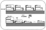
图10为本发明中同时具有SBD和DUV LED结构的集成光电子芯片的工作原理图,其中,图10(a)为本发明的方法中,AC工作下的电路图,图10(b)为滤波前和滤波后的驱动电压信号波形图,图10(c)为用传统的整流结构整流前和整流后的驱动电压信号波形图。Fig. 10 is the working principle diagram of the integrated optoelectronic chip with both SBD and DUV LED structures in the present invention, wherein Fig. 10(a) is the circuit diagram under AC operation in the method of the present invention, and Fig. 10(b) is the circuit diagram before filtering Figure 10(c) shows the waveforms of the driving voltage signal before and after rectification using the traditional rectification structure.
图11为本发明的方法中,通过上述工艺实现的同时具有SBD和DUV LED结构的集成光电子芯片图。11 is a diagram of an integrated optoelectronic chip having both SBD and DUV LED structures realized by the above process in the method of the present invention.
图12为经过一系列工艺方法,最终形成的SBD之间串联、DUV LED串联以及SBD和DUV LED连接的器件图。Figure 12 is a device diagram of finally formed SBDs in series, DUV LEDs in series, and SBDs and DUV LEDs connected through a series of process methods.
图13为传统技术中一种桥式整流电路的结构图;13 is a structural diagram of a bridge rectifier circuit in the conventional technology;
图14为本发明实现的SBD和DUV LED的阵列图;Fig. 14 is the array diagram of SBD and DUV LED realized by the present invention;
图15为单个DUV LED以及同时具有SBD和DUV LED结构的器件外加反向偏压时的IV特性曲线的图;其中,图15(a)为单个DUV LED外加反向偏压时的IV特性曲线,图15(b)为同时具有SBD和DUV LED结构的器件外加反向偏压时的IV特性曲线;Figure 15 is a graph of the IV characteristic curve of a single DUV LED and a device with both SBD and DUV LED structures when reverse bias is applied; wherein, Figure 15(a) is the IV characteristic curve of a single DUV LED when reverse bias is applied , Figure 15(b) is the IV characteristic curve of the device with both SBD and DUV LED structures when reverse bias is applied;
其中,1,衬底;2,缓冲层;3,n-AlGaN层;4,本征AlGaN层;5,n-AlGaN电子传输层;6,多量子阱层;7,p-AlGaN电子阻挡层;8,p-AlGaN/p-GaN空穴注入层;9,电流扩展层;10,DUVLED的p-型欧姆电极;11,DUV LED的n-型欧姆电极;11,SBD的n-型欧姆接触电极;12,SBD的肖特基接触电极。Among them, 1, substrate; 2, buffer layer; 3, n-AlGaN layer; 4, intrinsic AlGaN layer; 5, n-AlGaN electron transport layer; 6, multiple quantum well layer; 7, p-AlGaN electron blocking layer ; 8, p-AlGaN/p-GaN hole injection layer; 9, current spreading layer; 10, p-type ohmic electrode of DUVLED; 11, n-type ohmic electrode of DUV LED; 11, n-type ohmic electrode of SBD Contact electrode; 12, Schottky contact electrode of SBD.
具体实施方式Detailed ways
下面结合实施例及附图对本发明作进一步说明,但不以此作为对本申请权利要求保护范围的限定。The present invention will be further described below with reference to the embodiments and the accompanying drawings, but this is not intended to limit the protection scope of the claims of the present application.
本发明的同时具有SBD和DUV LED结构的集成光电子芯片结构如图14所示,包括排列为一行的n个SBD器件(n=1~25),以及位于其下的n列*m行(m=4~50)的DUV LED;所述的SBD和DUV LED呈阵列排布;The integrated optoelectronic chip structure with both SBD and DUV LED structures of the present invention is shown in FIG. 14 , including n SBD devices (n=1-25) arranged in one row, and n columns*m rows (m =4 to 50) DUV LEDs; the SBD and DUV LEDs are arranged in an array;
其中,n个SBD器件为串联,右端的欧姆接触电极和上面的条形芯片电极相连;左端的肖特基接触电极和下一行正下方的DUV LED的n型欧姆电极相连,DUV LED的p型欧姆电极和相邻的DUV LED的n型欧姆电极相连;n列*m行的DUV LED呈蛇形排列串联;最下行的尾端的DUV LED的p型欧姆电极与下部的条形芯片电极相连;电极之间通过金属连接,所述的金属为Ni/Au、Cr/Au、Pt/Au或Ni/Al;Among them, n SBD devices are connected in series, and the ohmic contact electrode at the right end is connected with the upper strip chip electrode; the Schottky contact electrode at the left end is connected with the n-type ohmic electrode of the DUV LED directly below the next row, and the p-type DUV LED is connected. The ohmic electrode is connected with the n-type ohmic electrode of the adjacent DUV LED; the DUV LEDs in n columns*m rows are arranged in series in a serpentine shape; the p-type ohmic electrode of the DUV LED at the end of the lowest row is connected with the lower strip chip electrode; The electrodes are connected by metal, and the metal is Ni/Au, Cr/Au, Pt/Au or Ni/Al;
所述的SBD和DUV LED共用一个相同的衬底和缓冲层2;The SBD and DUV LEDs share the same substrate and
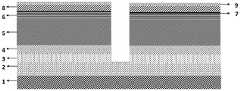
如图1所示,在DUV LED中,缓冲层2上依次为n-AlGaN层3、本征AlGaN层4、n-AlGaN电子传输层5;所述的n-AlGaN电子传输层5为上、下层两部分,上层为下层投影面积的80%,上层厚度为下层厚度的10%~25%;n-AlGaN电子传输层5的上层依次覆盖有多量子阱层6、p-AlGaN电子阻挡层7、p-AlGaN/p-GaN空穴注入层8、电流扩展层9;电流扩展层9上还部分覆盖有p-型欧姆电极10,p-型欧姆电极10面积为电流扩展层9面积的5%~100%;n-AlGaN电子传输层5的下层上表面的暴露部分还部分覆盖有n型欧姆电极11,n型欧姆电极11面积为n-AlGaN电子传输层5的下层的暴露部分面积的5%~95%;n-AlGaN层3、本征AlGaN层4、n-AlGaN电子传输层5、多量子阱层6、p-AlGaN电子阻挡层7、p-AlGaN/p-GaN空穴注入层8、电流扩展层9的侧部,以及电流扩展层9上表面的暴露部分、n-AlGaN电子传输层5的下层的暴露部分覆盖有绝缘钝化层;As shown in FIG. 1, in the DUV LED, the buffer layer 2 is sequentially formed by an n-AlGaN layer 3, an intrinsic AlGaN layer 4, and an n-AlGaN electron transport layer 5; the n-AlGaN electron transport layer 5 is the upper, There are two parts of the lower layer, the upper layer is 80% of the projected area of the lower layer, and the thickness of the upper layer is 10% to 25% of the thickness of the lower layer; the upper layer of the n-AlGaN electron transport layer 5 is sequentially covered with a multiple quantum well layer 6 and a p-AlGaN electron blocking layer 7 , p-AlGaN/p-GaN hole injection layer 8, current spreading layer 9; the current spreading layer 9 is also partially covered with a p-type ohmic electrode 10, and the area of the p-type ohmic electrode 10 is 5% of the area of the current spreading layer 9 %~100%; the exposed part of the upper surface of the lower layer of the n-AlGaN electron transport layer 5 is also partially covered with the n-type ohmic electrode 11 , and the area of the n-type ohmic electrode 11 is equal to the area of the exposed part of the lower layer of the n-AlGaN electron transport layer 5 . 5%~95%; n-
在SBD中,缓冲层2上为n-AlGaN层3,n-AlGaN层3上表面的40%~60%覆盖有本征AlGaN层4;n-AlGaN层3的暴露部分的5%~100%覆盖有n型欧姆电极11,本征AlGaN层4的5%~100%覆盖有肖特基接触电极12。In the SBD, the
即在图1中,深紫外发光二极管器件(DUV LED)沿着外延生长方向依次包括:衬底1、缓冲层2、n-AlGaN层3、本征AlGaN层4、n-AlGaN电子传输层5、多量子阱层6、p-AlGaN电子阻挡层7、p-AlGaN/p-GaN空穴注入层8、电流扩展层9、p-型欧姆电极10和n-型欧姆电极11;SBD器件沿着外延方向依次为衬底1、缓冲层2、n-AlGaN层3、本征AlGaN层4、n-型欧姆接触电极11、肖特基接触电极12(图1左侧框中的器件结构为DUV LED,右侧框中的器件结构为SBD)。That is, in FIG. 1, the deep ultraviolet light emitting diode device (DUV LED) sequentially includes along the epitaxial growth direction:
图2是通过MOCVD技术生长出来的初始基片,在初始基片的基础上再通过一系列的技术手段实现图1所示的成品芯片。FIG. 2 is an initial substrate grown by MOCVD technology. On the basis of the initial substrate, a series of technical means are used to realize the finished chip shown in FIG. 1 .
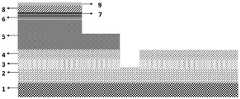
图3所示表明,在图2的初始基片上通过光刻和深刻蚀工艺,刻蚀至缓冲层2位置,将单个器件隔离。As shown in FIG. 3, it is shown that the initial substrate of FIG. 2 is etched to the position of the
图4所示表明,在图3的器件隔离之后通过光刻和干法刻蚀工艺制作台阶,将DUVLED一侧曝露出n-AlGaN电子传输层5。As shown in FIG. 4 , after the device of FIG. 3 is isolated, steps are formed by photolithography and dry etching processes, and the n-AlGaN
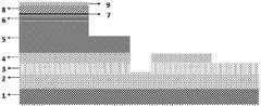
图5所示表明,在图4之后通过光刻和干法刻蚀工艺制作台阶,对于SBD器件将整个器件暴露至本征AlGaN层4。As shown in FIG. 5, it is shown that the steps are fabricated by photolithography and dry etching process after FIG. 4, exposing the entire device to the
图6所示表明,在图5实现的SBD器件一侧,通过光刻和干法刻蚀工艺制作台阶并暴露至n-AlGaN层3。As shown in FIG. 6 , on the side of the SBD device realized in FIG. 5 , the steps are fabricated and exposed to the n-
图7所示表明,在图6制作的基片基础上利用PECVD技术生长绝缘钝化层。As shown in FIG. 7 , the insulating passivation layer is grown by PECVD technology on the basis of the substrate produced in FIG. 6 .
图8所示表明,通过光刻和湿法刻蚀技术,刻蚀掉深紫外发光二极管的p-型欧姆电极和n-型欧姆电极以及SBD器件的n-型欧姆电极和肖特基接触电极位置表面的绝缘钝化层,为下一步制作电极做准备。Figure 8 shows that the p-type ohmic electrode and n-type ohmic electrode of deep ultraviolet light emitting diode and the n-type ohmic electrode and Schottky contact electrode of SBD device are etched away by photolithography and wet etching technology The insulating passivation layer on the surface of the position is prepared for the next step of making electrodes.
图9所示表明,在图8的基础上通过光刻和电子束蒸镀技术,制作DUV LED器件和SBD器件的电极,以及分立器件之间的互联金属电极。Figure 9 shows that, on the basis of Figure 8, electrodes for DUV LED devices and SBD devices, as well as interconnecting metal electrodes between discrete devices, are fabricated by photolithography and electron beam evaporation techniques.
图10中,图10(a)所示表明AC工作下的电路图,图10(b)为滤波前和滤波后的驱动电压信号波形图,图10(c)为用传统的整流结构整流前和整流后的驱动电压信号波形图。图10(b)滤波后的驱动电压变为间断脉冲直流电,这与图10(c)中传统整流后的不间断的直流电相比,间断式脉冲直流电供电给DUV LED,可以减少DUV LED结构的器件热效应,改善器件性能,提高器件使用寿命。In Fig. 10, Fig. 10(a) shows the circuit diagram under AC operation, Fig. 10(b) is the waveform diagram of the driving voltage signal before and after filtering, and Fig. 10(c) is the traditional rectification structure before and after rectification and The waveform diagram of the rectified driving voltage signal. Figure 10(b) The filtered driving voltage becomes intermittent pulsed DC, which is compared with the uninterrupted DC after traditional rectification in Figure 10(c). Device thermal effect, improve device performance, and increase device service life.
图11所示表明,通过工艺实现完整的一种同时具有SBD和DUV LED结构的集成光电子芯片结构示意图。Figure 11 shows that a complete integrated optoelectronic chip structure with both SBD and DUV LED structures is realized through the process.
图12所示表明最终形成的SBD之间串联、DUV LED串联以及SBD和DUV LED连接的器件图。Figure 12 shows a device diagram showing the resulting series between SBDs, DUV LEDs in series, and SBD and DUV LED connections.
图13所示表明传统技术中一种桥式整流电路的结构图;基于以上步骤可制作出本发明提出的一种同时具有肖特基的二极管(SBD)和深紫外发光二极管(DUV LED)的集成光电子芯片,该集成光电子芯片可以直接由市路电压(220V交流电)供电,省去了传统电路接入的LED驱动器,简化了电路,提高了发光效率和器件可靠性;此外,利用SBD的单向导通特性,该集成光电子芯片可实现对AC信号的滤波作用(如图10(b)所示,将正弦交流电的负偏压滤掉,只保留正偏压),即间接实现脉冲信号下的驱动模式,则可以减小LED的发热,延长器件使用寿命,更有利于LED的普及。FIG. 13 shows the structure diagram of a bridge rectifier circuit in the traditional technology; based on the above steps, a diode (SBD) with both Schottky and deep ultraviolet light emitting diode (DUV LED) proposed by the present invention can be fabricated Integrated optoelectronic chip, the integrated optoelectronic chip can be directly powered by the city voltage (220V AC), eliminating the need for the LED driver connected to the traditional circuit, simplifying the circuit, improving the luminous efficiency and device reliability; With the conduction characteristic, the integrated optoelectronic chip can filter the AC signal (as shown in Figure 10(b), the negative bias voltage of the sinusoidal AC current is filtered out, and only the positive bias voltage is retained), that is, it indirectly realizes the filtering effect under the pulse signal. The driving mode can reduce the heat generation of the LED, prolong the service life of the device, and be more conducive to the popularization of the LED.
当该集成光电子芯片处于正向偏压时(即AC信号的正半周期),SBD处于导通状态,与SBD串联的DUV LED亦处于导通状态,则该集成光电子芯片允许电流的输运并产生光子;从理论角度考虑,当外加反向偏压时(即AC信号的另一负半周期),SBD处于关断状态,则整个串联电路断开,此时没有电流通过DUV LED,因此该集成光电子芯片不会产生光子。从实际角度考虑,该集成光电子芯片中的SBD是基于AlGaN层,该层禁带宽度大、临界电场高,所以SBD可承担较高的击穿电压,同时漏电流较小,所以当集成光电子芯片外加反向偏压时不足以使DUV LED击穿(LED的击穿电压远小于SBD,所以当外加反向偏压时,从而起到保护整个电路的作用(DUV LED的反向击穿电压相比于SBD很小,所以如果电路中没有SBD承担较大的反向电压,LED很容易击穿,器件很容易损坏)。正是利用以上所述的SBD结构的单向导通性和可承担较大的反向击穿电压的特点,此集成光电子芯片不仅可以将正弦交流电转为脉冲的直流电,可以实现市路电压直接对此芯片的供电,还可以减少LED的发热现象,提高器件效率,增加器件使用寿命。When the integrated optoelectronic chip is in forward bias (that is, the positive half cycle of the AC signal), the SBD is in the on state, and the DUV LED connected in series with the SBD is also in the on state, the integrated optoelectronic chip allows the current to be transported and Photons are generated; from a theoretical point of view, when a reverse bias is applied (that is, another negative half cycle of the AC signal), the SBD is in the off state, the entire series circuit is disconnected, and no current passes through the DUV LED at this time, so the Integrated optoelectronic chips do not generate photons. From a practical point of view, the SBD in the integrated optoelectronic chip is based on the AlGaN layer, which has a large band gap and a high critical electric field, so the SBD can bear a higher breakdown voltage and has a small leakage current, so when the integrated optoelectronic chip is used When the reverse bias is applied, it is not enough to make the DUV LED breakdown (the breakdown voltage of the LED is much smaller than that of the SBD, so when the reverse bias is applied, it protects the entire circuit (the reverse breakdown voltage of the DUV LED is the same as that of the SBD). It is smaller than SBD, so if there is no SBD in the circuit to bear a large reverse voltage, the LED is easily broken down and the device is easily damaged). With the characteristics of large reverse breakdown voltage, this integrated optoelectronic chip can not only convert sinusoidal alternating current into pulsed direct current, but also directly supply power to the chip from the mains voltage, but also reduce the heating phenomenon of LED, improve device efficiency, increase Device life.
实施例1Example 1
一种同时具有SBD和DUV LED结构的集成光电子芯片,该芯片具有6个SBD结构和36个DUV LED结构(如图14所示),DUV LED沿着外延生长方向依次包括:衬底1、缓冲层2,厚度为30nm;n-AlGaN层3,厚度为1.5μm;本征的AlGaN层4,厚度为1.5μm;n-AlGaN电子传输层5,其中n-AlGaN电子传输层5分为两部分,下层厚度为3μm,上层厚度为0.5μm,上层为下层投影面积的80%;AlGaN/AlGaN多量子阱层6,量子阱和量子垒的厚度分别为3nm和10nm,共6对;p-AlGaN电子阻挡层7,厚度为15nm;p-AlGaN/p-GaN空穴注入层8,厚度为250nm;电流扩展层9,厚度为20nm;p-型欧姆电极10和n-型欧姆电极11,其中p-型欧姆电极10位于电流扩展层9的上方,厚度为200nm,p-型欧姆电极10面积为电流扩展层9面积的50%;n-型欧姆电极11位于n-AlGaN电子传输层5的暴露部分的上侧,厚度为200nm,n型欧姆电极面积为n-AlGaN电子传输层5的下层的暴露部分面积的50%;SBD器件沿着外延方向依次为衬底1、缓冲层2、n-AlGaN层3、本征AlGaN层4,本征AlGaN层4面积为n-AlGaN层3面积的40%,肖特基接触电极12位于本征AlGaN层4的上方,厚度为200nm,肖特基接触电极12面积为本征AlGaN层4面积的50%;n-型欧姆接触电极11位于n-AlGaN层暴露部分的上侧,厚度为200nm。不同器件之间有150nm厚的SiO2绝缘钝化层,再通过金属布线相互连接,DUV LED和SBD结构之间、相同DUVLED之间、相同SBD之间均有10μm的间隔距离,也就是图14中阵列之间的相邻间距。An integrated optoelectronic chip with both SBD and DUV LED structures, the chip has 6 SBD structures and 36 DUV LED structures (as shown in Figure 14), the DUV LEDs sequentially include along the epitaxial growth direction: substrate 1, buffer layer 2 with a thickness of 30nm; n-AlGaN layer 3 with a thickness of 1.5μm; intrinsic AlGaN layer 4 with a thickness of 1.5μm; n-AlGaN electron transport layer 5, wherein the n-AlGaN electron transport layer 5 is divided into two parts , the thickness of the lower layer is 3 μm, the thickness of the upper layer is 0.5 μm, and the upper layer is 80% of the projected area of the lower layer; AlGaN/AlGaN multiple quantum well layer 6, the thickness of quantum well and quantum barrier are 3 nm and 10 nm respectively, a total of 6 pairs; p-AlGaN Electron blocking layer 7 with a thickness of 15 nm; p-AlGaN/p-GaN hole injection layer 8 with a thickness of 250 nm; current spreading layer 9 with a thickness of 20 nm; p-type ohmic electrode 10 and n-type ohmic electrode 11, wherein The p-type ohmic electrode 10 is located above the current spreading layer 9 with a thickness of 200 nm, and the area of the p-type ohmic electrode 10 is 50% of the area of the current spreading layer 9 ; the n-type ohmic electrode 11 is located on the side of the n-AlGaN electron transport layer 5 The upper side of the exposed part has a thickness of 200 nm, and the area of the n-type ohmic electrode is 50% of the area of the exposed part of the lower layer of the n-AlGaN electron transport layer 5; the SBD device is followed by substrate 1, buffer layer 2, n -AlGaN layer 3, intrinsic AlGaN layer 4, the area of the intrinsic AlGaN layer 4 is 40% of the area of the n-AlGaN layer 3, the Schottky contact electrode 12 is located above the intrinsic AlGaN layer 4, the thickness is 200nm, the Schottky The area of the contact electrode 12 is 50% of the area of the intrinsic AlGaN layer 4; the n-type ohmic contact electrode 11 is located on the upper side of the exposed part of the n-AlGaN layer, and has a thickness of 200 nm. There is a 150nm-thickSiO2 insulating passivation layer between different devices, and they are connected to each other through metal wiring. There is a 10μm separation distance between DUV LED and SBD structure, between the same DUVLED, and between the same SBD, that is, Figure 14 Adjacent spacing between arrays in .
每个SBD的尺寸为50μm x 50μm;DUV LED的尺寸为350μm x 350μm;Each SBD measures 50μm x 50μm; DUV LED measures 350μm x 350μm;
整体器件尺寸为2300μm x 2200μm。The overall device size is 2300μm x 2200μm.
所述的DUV LED的p型欧姆电极材质为Ni/Al,n型欧姆电极材质为Ti/Al/Ti/Au;所述的SBD的欧姆电极材质为Ti/Al/Ti/Au,肖特基接触电极材质为Ni/Au。The p-type ohmic electrode material of the DUV LED is Ni/Al, the n-type ohmic electrode material is Ti/Al/Ti/Au; the ohmic electrode material of the SBD is Ti/Al/Ti/Au, and the Schottky electrode material is Ti/Al/Ti/Au. The contact electrode material is Ni/Au.
所述的上述一种同时具有SBD和DUV LED结构的集成光电子芯片,其制备方法如下:The above-mentioned integrated optoelectronic chip with SBD and DUV LED structures at the same time, its preparation method is as follows:
第一步,在MOCVD反应炉中,将衬底1在1300℃高温环境下进行烘烤,将衬底1表面的异物进行清除,然后分别生长缓冲层2;n-AlGaN层3;本征AlGaN层4;n-AlGaN电子传输层5;6对Al0.45Ga0.55N/Al0.55Ga0.45N多量子阱层6;p-Al0.6Ga0.4N电子阻挡层7;p-Al0.4Ga0.6N/p-GaN空穴注入层8。The first step is to bake the
第二步,在第一步得到的p-Al0.4Ga0.6N/p-GaN空穴注入层8上,通过蒸镀制作电流扩展层9,其材料是Ni/Au,厚度为20nm。In the second step, on the p-Al0.4 Ga0.6 N/p-GaN
第三步,在第二步得到的基片上通过光刻和深刻蚀工艺,选择性刻蚀至缓冲层2位置,形成器件阵列,将单个SBD、DUV LED器件隔离;阵列中,DUV LED、SBD器件之间有10μm的间距。In the third step, the substrate obtained in the second step is selectively etched to the position of the
第四步,在第三步得到的基片上通过光刻和干法刻蚀工艺制作台阶,将DUV LED一侧暴露出n-AlGaN电子传输层5,对于SBD器件使用相同的方法使器件暴露出本征AlGaN层4和n-AlGaN层3。The fourth step is to make steps on the substrate obtained in the third step by photolithography and dry etching, exposing the n-AlGaN
第五步,在第四得到的基片基础上通过PECVD技术生长绝缘钝化层以及绝缘间隔层,厚度为20-200nm。In the fifth step, an insulating passivation layer and an insulating spacer layer are grown by PECVD technology on the basis of the substrate obtained in the fourth step, and the thickness is 20-200 nm.
第六步,在第五步的基础上通过光刻和湿法刻蚀,刻蚀出DUV LED的n-型欧姆电极和p-型欧姆电极以及SBD的n-型欧姆电极和肖特基接触电极位置处覆盖的绝缘层,为下一步制作电极做准备。In the sixth step, on the basis of the fifth step, the n-type ohmic electrode and p-type ohmic electrode of DUV LED and the n-type ohmic electrode and Schottky contact of SBD are etched through photolithography and wet etching. The insulating layer covering the electrode position prepares the electrode for the next step.
第七步,在第六步刻蚀出的电极位置,通过光刻和电子束蒸镀技术制作DUV LED和SBD的电极,以及实现分立器件连接的互联金属电极。In the seventh step, at the electrode positions etched in the sixth step, the electrodes of the DUV LED and the SBD, and the interconnected metal electrodes for realizing the connection of the discrete devices are fabricated by photolithography and electron beam evaporation technology.
由此制得本发明的一种同时具有SBD和DUV LED结构的集成光电子芯片。Thereby, an integrated optoelectronic chip of the present invention having both SBD and DUV LED structures is prepared.
从上面实施例可以看出,本发明由于利用SBD可以把交流电的负半部分滤掉,只保留正半部分,即只有外加正半部分的电压时DUV LED才会导通发光,而负半部分的电压因为被SBD滤掉,所以DUV LED不会导通;相比于直接把交流电的负半部分通过某种手段变成正的,会使DUV LED在通电期间一直处于导通发光状态,而我们所提出的结构中,DUV LED在外加负半部分电压时处于不亮的状态,相当于只有一半的电压可以使DUV LED导通,所以从理论上推测,本专利所提出的结构可以减少一倍的发热,增加器件的使用寿命。It can be seen from the above embodiment that the present invention can filter out the negative half of the alternating current due to the use of SBD, and only retain the positive half, that is, the DUV LED will turn on and emit light only when the voltage of the positive half is applied, while the negative half Because the voltage of the DUV LED is filtered by the SBD, the DUV LED will not be turned on; compared with directly turning the negative half of the AC power into positive by some means, the DUV LED will always be turned on and emit light during the power-on period, and In the structure proposed by us, the DUV LED is in a non-lighting state when the negative half voltage is applied, which is equivalent to only half of the voltage can make the DUV LED turn on. Therefore, it is theoretically speculated that the structure proposed in this patent can reduce one times the heat and increase the service life of the device.
上述实施例仅是本发明的优选实施方式,应当指出:对于本技术领域的普通技术人员来说,在不脱离本发明原理的前提下,还可以做出若干改进和等同替换,这些对本发明权利要求进行改进和等同替换后的技术方案后的技术方案,均落于本发明的保护范围。The above-mentioned embodiments are only the preferred embodiments of the present invention. It should be pointed out that for those skilled in the art, without departing from the principles of the present invention, several improvements and equivalent replacements can be made. The technical solutions required to be improved and equivalent to the replaced technical solutions all fall within the protection scope of the present invention.
本发明未尽事宜为公知技术。Matters not addressed in the present invention are known in the art.
由此制得本发明的一种同时具有SBD和DUV LED结构的集成光电子芯片。Thereby, an integrated optoelectronic chip of the present invention having both SBD and DUV LED structures is prepared.
图15为通过Crosslight公司的APSYS软件仿真计算得到的单个DUV LED结构以及同时具有DUV LED和SBD结构的反向IV特性,图15(a)为单个DUV LED结构的反向IV特性曲线,单个DUV LED结构的击穿电压为14V,图15(b)为同时具有SBD和DUV LED结构的反向IV特性曲线,而同时具有DUV LED和SBD结构的击穿电压可以提高到1000V左右,可见我们提出的器件结构可以有效提高器件的反向击穿电压,从而起到保护电路的作用。Figure 15 shows the single DUV LED structure and the reverse IV characteristic with both DUV LED and SBD structure calculated by APSYS software of Crosslight Company. Figure 15(a) is the reverse IV characteristic curve of a single DUV LED structure. The breakdown voltage of the LED structure is 14V. Figure 15(b) shows the reverse IV characteristic curve of both SBD and DUV LED structures, while the breakdown voltage of both DUV LED and SBD structures can be increased to about 1000V. It can be seen that our proposed The device structure can effectively improve the reverse breakdown voltage of the device, thereby playing the role of protecting the circuit.
通过以上实施例,我们所提出的具有SBD结构的发光二极管器件不需要LED驱动器,可以直接由市路电压供电,这样不仅电路简单明了,还可以降低成本。本发明提出而一种具有肖特基的二极管(SBD)和的深紫外发光二极管(DUV LED)集成的光电子芯片,可以直接由市路电压供电,省去了LED驱动器,简化了电路,提高了发光效率和器件可靠性;此外,利用SBD的单向导通特性,该集成光电子芯片可实现对AC信号的滤波作用,即间接实现脉冲信号下的驱动模式,则可以减小LED的发热,延长器件使用寿命,更有利于LED的普及。Through the above embodiments, the light emitting diode device with the SBD structure proposed by us does not need an LED driver, and can be directly powered by the mains voltage, which not only has a simple and clear circuit, but also can reduce costs. The invention proposes an optoelectronic chip with Schottky diode (SBD) and deep ultraviolet light emitting diode (DUV LED) integrated, which can be directly powered by the mains voltage, saves the LED driver, simplifies the circuit, and improves the Luminous efficiency and device reliability; in addition, using the unidirectional conduction characteristics of SBD, the integrated optoelectronic chip can filter the AC signal, that is, indirectly realize the driving mode under the pulse signal, which can reduce the heating of the LED and prolong the device. The service life is more conducive to the popularization of LEDs.
当该集成光电子芯片处于正向偏压时(即AC信号的一半周期),SBD处于导通状态,与SBD串联的DUV LED亦处于导通状态,则该集成光电子芯片允许电流的输运并产生光子;从理论角度考虑,当外加反向偏压时(即AC信号的另一半周期),SBD处于关断状态,则整个串联电路断开,没有电流通过DUV LED,因此该集成光电子芯片不会产生光子。从实际角度考虑,该集成光电子芯片中的SBD是基于AlGaN层,该层禁带宽度大、临界电场高,所以SBD可承担较高的击穿电压,同时漏电流较小,不足以使DUV LED击穿,从而起到保护整个电路的作用。When the integrated optoelectronic chip is in forward bias (that is, half cycle of the AC signal), the SBD is in a conducting state, and the DUV LED connected in series with the SBD is also in a conducting state, then the integrated optoelectronic chip allows the transport of current and generates Photon; from a theoretical point of view, when a reverse bias is applied (ie, the other half cycle of the AC signal), the SBD is in the off state, the entire series circuit is disconnected, and no current passes through the DUV LED, so the integrated optoelectronic chip will not produce photons. From a practical point of view, the SBD in the integrated optoelectronic chip is based on the AlGaN layer, which has a large forbidden band width and a high critical electric field, so the SBD can bear a high breakdown voltage, while the leakage current is small, which is not enough to make DUV LEDs. breakdown, thereby protecting the entire circuit.
本发明未尽事宜为公知技术。Matters not addressed in the present invention are known in the art.
Claims (2)
Translated fromChinesePriority Applications (1)
| Application Number | Priority Date | Filing Date | Title |
|---|---|---|---|
| CN202010750824.6ACN111863861B (en) | 2020-07-28 | 2020-07-28 | Integrated photoelectronic chip structure with SBD and DUV LEDs and preparation method thereof |
Applications Claiming Priority (1)
| Application Number | Priority Date | Filing Date | Title |
|---|---|---|---|
| CN202010750824.6ACN111863861B (en) | 2020-07-28 | 2020-07-28 | Integrated photoelectronic chip structure with SBD and DUV LEDs and preparation method thereof |
Publications (2)
| Publication Number | Publication Date |
|---|---|
| CN111863861A CN111863861A (en) | 2020-10-30 |
| CN111863861Btrue CN111863861B (en) | 2022-08-30 |
Family
ID=72945154
Family Applications (1)
| Application Number | Title | Priority Date | Filing Date |
|---|---|---|---|
| CN202010750824.6AActiveCN111863861B (en) | 2020-07-28 | 2020-07-28 | Integrated photoelectronic chip structure with SBD and DUV LEDs and preparation method thereof |
Country Status (1)
| Country | Link |
|---|---|
| CN (1) | CN111863861B (en) |
Families Citing this family (2)
| Publication number | Priority date | Publication date | Assignee | Title |
|---|---|---|---|---|
| CN112563381B (en)* | 2020-12-29 | 2022-04-05 | 中国科学院长春光学精密机械与物理研究所 | A kind of deep ultraviolet light emitting diode with low ohmic contact resistance and preparation method thereof |
| CN114400262A (en)* | 2022-01-18 | 2022-04-26 | 南京邮电大学 | Gallium nitride optoelectronic integrated chip and preparation method thereof |
Citations (6)
| Publication number | Priority date | Publication date | Assignee | Title |
|---|---|---|---|---|
| EP0884217A1 (en)* | 1997-06-12 | 1998-12-16 | VIBRACHOC, Société Anonyme dite: | Lighting device for dashboard |
| CN101515615A (en)* | 2009-03-31 | 2009-08-26 | 西安电子科技大学 | AlGaN-based multiple quantum well uv-LED device based on SiC substrate and manufacturing method |
| CN102354481A (en)* | 2011-10-26 | 2012-02-15 | 吉林大学 | Alternating current LED (light-emitting diode) display array based on single crystal wafer |
| US9653642B1 (en)* | 2014-12-23 | 2017-05-16 | Soraa Laser Diode, Inc. | Manufacturable RGB display based on thin film gallium and nitrogen containing light emitting diodes |
| CN111223970A (en)* | 2014-07-29 | 2020-06-02 | 首尔伟傲世有限公司 | light-emitting device |
| CN111326632A (en)* | 2020-03-08 | 2020-06-23 | 河北工业大学 | AC Micro-LED Array with Trapezoidal Sidewall Field Plate Schottky Diodes |
Family Cites Families (1)
| Publication number | Priority date | Publication date | Assignee | Title |
|---|---|---|---|---|
| US8076699B2 (en)* | 2008-04-02 | 2011-12-13 | The Hong Kong Univ. Of Science And Technology | Integrated HEMT and lateral field-effect rectifier combinations, methods, and systems |
- 2020
- 2020-07-28CNCN202010750824.6Apatent/CN111863861B/enactiveActive
Patent Citations (6)
| Publication number | Priority date | Publication date | Assignee | Title |
|---|---|---|---|---|
| EP0884217A1 (en)* | 1997-06-12 | 1998-12-16 | VIBRACHOC, Société Anonyme dite: | Lighting device for dashboard |
| CN101515615A (en)* | 2009-03-31 | 2009-08-26 | 西安电子科技大学 | AlGaN-based multiple quantum well uv-LED device based on SiC substrate and manufacturing method |
| CN102354481A (en)* | 2011-10-26 | 2012-02-15 | 吉林大学 | Alternating current LED (light-emitting diode) display array based on single crystal wafer |
| CN111223970A (en)* | 2014-07-29 | 2020-06-02 | 首尔伟傲世有限公司 | light-emitting device |
| US9653642B1 (en)* | 2014-12-23 | 2017-05-16 | Soraa Laser Diode, Inc. | Manufacturable RGB display based on thin film gallium and nitrogen containing light emitting diodes |
| CN111326632A (en)* | 2020-03-08 | 2020-06-23 | 河北工业大学 | AC Micro-LED Array with Trapezoidal Sidewall Field Plate Schottky Diodes |
Also Published As
| Publication number | Publication date |
|---|---|
| CN111863861A (en) | 2020-10-30 |
Similar Documents
| Publication | Publication Date | Title |
|---|---|---|
| CN102509731B (en) | Alternating current vertical light emitting element and manufacture method thereof | |
| CN105720156B (en) | A kind of light emitting diode and preparation method thereof | |
| CN103219352B (en) | LED combination chip of array architecture and preparation method thereof | |
| CN111863861B (en) | Integrated photoelectronic chip structure with SBD and DUV LEDs and preparation method thereof | |
| CN102257619A (en) | Light emitting element | |
| CN101656260A (en) | An antistatic GaN-based light-emitting device and its manufacturing method | |
| CN103647009A (en) | Nitride light emitting diode and manufacturing method thereof | |
| CN104835893A (en) | Nitrogen polar surface LED based on metal nitride semiconductor and preparation method | |
| TWI538184B (en) | Light-emitting diode array | |
| CN103996755B (en) | A kind of preparation method of iii-nitride light emitting devices assembly | |
| CN108538982A (en) | A kind of chip epitaxial structure of low-resistance LED and preparation method thereof | |
| CN103618042B (en) | A kind of semiconductor light-emitting diode chip | |
| CN103682022B (en) | LED device structure | |
| CN113851566B (en) | Deep ultraviolet LED flip chip and manufacturing method thereof | |
| CN106129205A (en) | A kind of LED chip of ito thin film structure and preparation method thereof | |
| CN106784231A (en) | LED chip and manufacturing method thereof | |
| JP5455852B2 (en) | Compound semiconductor light emitting device and method for manufacturing the same | |
| CN107452861A (en) | A kind of UV LED chip and preparation method thereof | |
| CN103311389A (en) | Light-emitting diode epitaxial wafer and manufacturing method thereof | |
| CN207529970U (en) | A kind of UV LED chip | |
| CN218039207U (en) | Monolithic integrated chip of HEMT and blue light LED | |
| CN217507340U (en) | Deep ultraviolet LED chip capable of improving optical power and reliability | |
| CN104752574A (en) | LED light emitting material | |
| CN100502071C (en) | Group III nitride semiconductor light-emitting diode based on planar structure and its preparation method | |
| KR101132885B1 (en) | Nitride light emitting diode and fabricating method thereof |
Legal Events
| Date | Code | Title | Description |
|---|---|---|---|
| PB01 | Publication | ||
| PB01 | Publication | ||
| SE01 | Entry into force of request for substantive examination | ||
| SE01 | Entry into force of request for substantive examination | ||
| GR01 | Patent grant | ||
| GR01 | Patent grant |