CN111863780A - Package structure and electronic equipment - Google Patents
Package structure and electronic equipmentDownload PDFInfo
- Publication number
- CN111863780A CN111863780ACN202010690817.1ACN202010690817ACN111863780ACN 111863780 ACN111863780 ACN 111863780ACN 202010690817 ACN202010690817 ACN 202010690817ACN 111863780 ACN111863780 ACN 111863780A
- Authority
- CN
- China
- Prior art keywords
- substrate
- pin
- flash memory
- chip
- electrically connected
- Prior art date
- Legal status (The legal status is an assumption and is not a legal conclusion. Google has not performed a legal analysis and makes no representation as to the accuracy of the status listed.)
- Pending
Links
Images


Classifications
- H—ELECTRICITY
- H01—ELECTRIC ELEMENTS
- H01L—SEMICONDUCTOR DEVICES NOT COVERED BY CLASS H10
- H01L25/00—Assemblies consisting of a plurality of semiconductor or other solid state devices
- H01L25/03—Assemblies consisting of a plurality of semiconductor or other solid state devices all the devices being of a type provided for in a single subclass of subclasses H10B, H10D, H10F, H10H, H10K or H10N, e.g. assemblies of rectifier diodes
- H01L25/04—Assemblies consisting of a plurality of semiconductor or other solid state devices all the devices being of a type provided for in a single subclass of subclasses H10B, H10D, H10F, H10H, H10K or H10N, e.g. assemblies of rectifier diodes the devices not having separate containers
- H01L25/065—Assemblies consisting of a plurality of semiconductor or other solid state devices all the devices being of a type provided for in a single subclass of subclasses H10B, H10D, H10F, H10H, H10K or H10N, e.g. assemblies of rectifier diodes the devices not having separate containers the devices being of a type provided for in group H10D89/00
- H01L25/0655—Assemblies consisting of a plurality of semiconductor or other solid state devices all the devices being of a type provided for in a single subclass of subclasses H10B, H10D, H10F, H10H, H10K or H10N, e.g. assemblies of rectifier diodes the devices not having separate containers the devices being of a type provided for in group H10D89/00 the devices being arranged next to each other
- G—PHYSICS
- G06—COMPUTING OR CALCULATING; COUNTING
- G06F—ELECTRIC DIGITAL DATA PROCESSING
- G06F15/00—Digital computers in general; Data processing equipment in general
- G06F15/16—Combinations of two or more digital computers each having at least an arithmetic unit, a program unit and a register, e.g. for a simultaneous processing of several programs
- G06F15/163—Interprocessor communication
- H—ELECTRICITY
- H01—ELECTRIC ELEMENTS
- H01L—SEMICONDUCTOR DEVICES NOT COVERED BY CLASS H10
- H01L23/00—Details of semiconductor or other solid state devices
- H01L23/52—Arrangements for conducting electric current within the device in operation from one component to another, i.e. interconnections, e.g. wires, lead frames
- H01L23/538—Arrangements for conducting electric current within the device in operation from one component to another, i.e. interconnections, e.g. wires, lead frames the interconnection structure between a plurality of semiconductor chips being formed on, or in, insulating substrates
Landscapes
- Engineering & Computer Science (AREA)
- Computer Hardware Design (AREA)
- Physics & Mathematics (AREA)
- General Physics & Mathematics (AREA)
- Microelectronics & Electronic Packaging (AREA)
- Power Engineering (AREA)
- Theoretical Computer Science (AREA)
- Condensed Matter Physics & Semiconductors (AREA)
- Software Systems (AREA)
- General Engineering & Computer Science (AREA)
- Semiconductor Memories (AREA)
- Semiconductor Integrated Circuits (AREA)
Abstract
Description
Translated fromChinese技术领域technical field
本申请涉及通信技术领域,尤其涉及一种封装结构及电子设备。The present application relates to the field of communication technologies, and in particular, to a packaging structure and an electronic device.
背景技术Background technique
随着技术的发展,智能电子设备的主板上设置的芯片也越来越多,比如闪存芯片、双倍速率同步动态随机存储器(Double Date Rate,DDR)芯片、计算芯片等,且各种芯片设置在主板上,并通过主板上的线路实现不同芯片间的数据交互。然而,随着应用需求的提高,现有的计算芯片和闪存芯片间的数据交互速度已经不能满足日益提高的交互速度需求,比如往DDR芯片上写数据就存在速度慢、功耗大的问题。With the development of technology, more and more chips are set on the motherboard of intelligent electronic devices, such as flash memory chips, double-rate synchronous dynamic random access memory (Double Date Rate, DDR) chips, computing chips, etc., and various chip settings On the main board, and through the lines on the main board, the data interaction between different chips is realized. However, with the increase of application requirements, the data interaction speed between existing computing chips and flash memory chips can no longer meet the increasing interaction speed requirements. For example, writing data to DDR chips has problems of slow speed and high power consumption.
可见,现有技术中,主板上的计算芯片和闪存芯片间的数据交互存在交互速度慢的问题。It can be seen that, in the prior art, the data interaction between the computing chip on the motherboard and the flash memory chip has the problem of slow interaction speed.
发明内容SUMMARY OF THE INVENTION
本申请实施例提供一种封装结构及电子设备,能够解决现有技术中,主板上的计算芯片和闪存芯片间的数据交互存在交互速度慢的问题。The embodiments of the present application provide a packaging structure and an electronic device, which can solve the problem of slow interaction speed in data interaction between a computing chip on a motherboard and a flash memory chip in the prior art.
为解决上述技术问题,本申请是这样实现的:In order to solve the above-mentioned technical problems, the present application is implemented as follows:
第一方面,本申请实施例提供了一种封装结构,包括:计算芯片、闪存芯片和第一基板,所述计算芯片和所述闪存芯片设于所述第一基板上,且所述计算芯片设有第一引脚,所述闪存芯片设有第二引脚,所述第一引脚通过设于所述第一基板上的硅互连结构与所述第二引脚电连接,所述计算芯片通过所述硅互连结构与所述闪存芯片进行通信。In a first aspect, an embodiment of the present application provides a packaging structure, including: a computing chip, a flash memory chip, and a first substrate, the computing chip and the flash memory chip are disposed on the first substrate, and the computing chip A first pin is provided, the flash memory chip is provided with a second pin, and the first pin is electrically connected to the second pin through a silicon interconnect structure provided on the first substrate, and the A computing chip communicates with the flash memory chip through the silicon interconnect structure.
第二方面,本申请实施例还提供一种电子设备,包括上述封装结构。In a second aspect, an embodiment of the present application further provides an electronic device, including the above-mentioned packaging structure.
在本申请实施例中,计算芯片与闪存芯片之间的通信,可以通过第一引脚和第二引脚进行通信连接来实现,且第一引脚和第二引脚之间可以通过硅互连结构进行电连接,以实现计算芯片和闪存芯片之间的通信交互,且并通过利用硅互连结构具有的功耗低、传输速度快的特点,采用硅互连结构实现计算芯片与闪存芯片的通信连接,可以有效提高计算芯片与闪存芯片之间的数据交互速度。In this embodiment of the present application, the communication between the computing chip and the flash memory chip can be realized by communicating between the first pin and the second pin, and the first pin and the second pin can be connected through silicon interconnection. The interconnection structure is electrically connected to realize the communication interaction between the computing chip and the flash memory chip, and by utilizing the low power consumption and fast transmission speed of the silicon interconnection structure, the silicon interconnection structure is used to realize the computing chip and the flash memory chip. The communication connection can effectively improve the data interaction speed between the computing chip and the flash memory chip.
附图说明Description of drawings
图1是本申请实施例提供的封装结构的结构图之一;1 is one of the structural diagrams of the packaging structure provided by an embodiment of the present application;
图2是本申请实施例提供的封装结构的结构图之二;FIG. 2 is the second structural diagram of the packaging structure provided by the embodiment of the present application;
图3是本申请实施例提供的封装结构的结构图之三;FIG. 3 is the third structural diagram of the packaging structure provided by the embodiment of the present application;
图4是本申请实施例提供的封装结构的结构图之四;FIG. 4 is a fourth structural diagram of a packaging structure provided by an embodiment of the present application;
图5是本申请实施例提供的封装结构的结构图之五;FIG. 5 is a fifth structural diagram of a packaging structure provided by an embodiment of the present application;
图6是本申请实施例提供的封装结构的结构图之六。FIG. 6 is a sixth structural diagram of the packaging structure provided by the embodiment of the present application.
具体实施方式Detailed ways
下面将结合本申请实施例中的附图,对本申请实施例中的技术方案进行清楚、完整地描述,显然,所描述的实施例是本申请一部分实施例,而不是全部的实施例。基于本申请中的实施例,本领域普通技术人员在没有作出创造性劳动前提下所获得的所有其他实施例,都属于本申请保护的范围。The technical solutions in the embodiments of the present application will be clearly and completely described below with reference to the accompanying drawings in the embodiments of the present application. Obviously, the described embodiments are part of the embodiments of the present application, not all of the embodiments. Based on the embodiments in the present application, all other embodiments obtained by those of ordinary skill in the art without creative work fall within the protection scope of the present application.
本申请的说明书和权利要求书中的术语“第一”、“第二”等是用于区别类似的对象,而不用于描述特定的顺序或先后次序。应该理解这样使用的数据在适当情况下可以互换,以便本申请的实施例能够以除了在这里图示或描述的那些以外的顺序实施。此外,说明书以及权利要求中“和/或”表示所连接对象的至少其中之一,字符“/”,一般表示前后关联对象是一种“或”的关系。The terms "first", "second" and the like in the description and claims of the present application are used to distinguish similar objects, and are not used to describe a specific order or sequence. It is to be understood that data so used may be interchanged under appropriate circumstances so that embodiments of the application can be practiced in sequences other than those illustrated or described herein. In addition, "and/or" in the description and claims indicates at least one of the connected objects, and the character "/" generally indicates that the associated objects are in an "or" relationship.
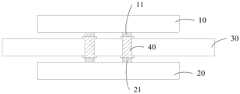
如图1至图6所示,本申请实施例提供一种封装结构,包括:计算芯片10、闪存芯片20和第一基板30,计算芯片10和闪存芯片20设于第一基板30上,计算芯片10设有第一引脚11,闪存芯片20设有第二引脚22,第一引脚11通过设于第一基板30上的硅互连结构40与第二引脚22电连接,计算芯片10通过硅互连结构40与闪存芯片20进行通信。As shown in FIG. 1 to FIG. 6 , an embodiment of the present application provides a package structure, including: a
本实施方式中,计算芯片10与闪存芯片20之间的通信,可以通过第一引脚11和第二引脚22进行通信连接来实现,且第一引脚11和第二引脚22之间可以通过硅互连结构40进行电连接,进而实现计算芯片10和闪存芯片20之间的通信交互。其中,硅互连结构40可以是采用全硅技术形成的硅结构,并用于实现计算芯片10与闪存芯片20的通信连接,且通过利用硅互连结构40具有功耗低、传输速度快的特点,因此相较于通过采用电路板上的印刷线路实现计算芯片10与闪存芯片20的通信连接,通过采用硅互连结构40实现计算芯片10与闪存芯片20的通信连接,可以有效提高计算芯片10与闪存芯片20之间的数据交互速度。In this embodiment, the communication between the
而且,由于通过采用硅互连结构40实现计算芯片10和闪存芯片20的通信连接,从而可以有效提高计算芯片10和闪存芯片20之间的数据交互速度。而且,相较于需要采用DDR芯片来辅助提高计算芯片10和闪存芯片20之间的数据交互速度,还能够降低封装结构的造价成本。Moreover, since the communication connection between the
进一步的,针对计算芯片10,还可以通过设置静态随机存储器、非易失性的随机存储器、阻变式存储器等片上存储,还可以进一步替换掉DDR芯片的作用,以便省去DDR芯片的使用,达到降低封装结构的造价成本的目的。Further, for the
可选的,计算芯片10和闪存芯片20均设于第一基板30的第一侧,且硅互连结构40的两端部在第一基板30的第一侧分别形成第一连接部(未图示)和第二连接部(未图示),第一连接部与第一引脚11电连接,第二连接部与第二引脚21电连接。Optionally, both the
本实施方式中,通过将硅互连结构40布线在第一基板30的第一侧,并形成第一连接部和第二连接部,可以降低硅互连结构40在第一基板30上的布线难度;而且,硅互连结构40可以通过第一连接部、第二连接部更好的与第一引脚11及第二引脚21进行电连接,改善硅互连结构40与第一引脚11和第二引脚21的连接效果。In this embodiment, by wiring the
另外,通过将计算芯片10和闪存芯片20设置在第一基板30的同一侧,可以有效降低封装结构的整体高度,从而使封装结构可以适配更多的安装场景。In addition, by arranging the
其中,硅互连结构40包括基部、第一连接部和第二连接部,第一连接部和第二连接部设置在基部的两端,基部以硅结构走线的形式设置在第一基板30上,并在第一基板30的第一侧形成并显露第一连接部和第二连接部,以便第一连接部与第一引脚11电连接,以及第二连接部与第二引脚21电连接,进而实现硅互连结构40对计算芯片10和闪存芯片20的通信连接。The
可选的,计算芯片10和闪存芯片20分别设于第一基板30的两相背侧,硅互连结构40贯穿第一基板30的厚度方向设置,并在第一基板30的两相背侧分别形成第三连接部(未图示)和第四连接部(未图示),第三连接部与第一引脚11电连接,第四连接部与第二引脚21电连接。Optionally, the
本实施方式中,通过将计算芯片10和闪存芯片20分别设于第一基板30的两相背侧,并通过贯穿第一基板30的厚度方向设置的硅互连结构40,实现计算芯片10和闪存芯片20的垂直互连,可以减小硅互连结构40长度,进而减小信号延迟,降低芯片间的功耗,实现计算芯片10和闪存芯片20的高速通讯,提升计算芯片10和闪存芯片20之间的数据交互速度。In this embodiment, by disposing the
其中,可以通过硅通孔(Through Silicon Via,TSV)技术在第一基板30上形成硅互连结构40。TSV技术是通过将铜、钨、多晶硅等导电物质填充在第一基板30的通孔内,从而在第一基板30上形成具有垂直电气互连功能的硅互连结构40。Wherein, the
可选的,封装结构还包括与第一基板30层叠设置的电路板50,电路板50设有供电器件(未图示);计算芯片10还设有第三引脚12,第三引脚12通过第一基板30上的第一线路31与供电器件电连接;闪存芯片20还设有第四引脚22,第四引脚22通过第一基板30上的第二线路32与供电器件电连接。Optionally, the package structure further includes a
本实施方式中,电路板50上的供电器件可以通过第一线路31和第三引脚12实现与计算芯片10的电连接,进而实现对计算芯片10进行供电;相应的,电路板50上的供电器件还可以通过第二线路32和第四引脚22实现与闪存芯片20的电连接,进而实现对闪存芯片20进行供电。In this embodiment, the power supply device on the
其中,供电器件可以是电源或者供电电路等。The power supply device may be a power supply or a power supply circuit or the like.
另外,第一线路31和第二线路32可以是硅连接线,从而提高计算芯片10及闪存芯片20与电路板50的供电器件之间的数据交互速度。In addition, the
可选的,封装结构还包括设于第一基板30和电路板50之间的第二基板60,第二基板60设有第三线路61和第四线路62;第三线路61的一端与供电器件电连接,另一端通过第一线路31与第三引脚12电连接;第四线路62的一端与供电器件电连接,另一端通过第二线路32与第四引脚22电连接。Optionally, the package structure further includes a
本实施方式中,通过设置第二基板60,可以提升封装结构的整体性。而且,还可以将计算芯片10、闪存芯片20、第一基板30和第二基板60作为一个单独的封装结构,这样可以方便将其组装到对应的电路板或者电子设备的主板上。In this embodiment, by disposing the
其中,第一连接线31可以通过常规的导线连接等电连接方式实现与第三线路61的电连接,或者与电路板50上的供电器件的电连接;第二连接线32也可以通过常规的导线连接等电连接方式实现与第四线路62的电连接,或者与电路板50上的供电器件的电连接。Wherein, the
另外,第三线路61和第四线路62也可以通过常规的导线连接等电连接方式实现与电路板50上的供电器件电连接。In addition, the
需要说明的是,设于第一基板30上的计算芯片10的数量可以是一个,或者多个,其数量可以根据实际需求进行设计;相应的,设于第一基板30上的闪存芯片20的数量也可以是一个,或者多个,且其数量可以根据实际需求进行设计。It should be noted that the number of
另外,第一基板30可以是硅连接板,硅连接板的主体材料是硅,具有良好的散热性和导热性。而且,计算芯片10和闪存芯片20的材料也可以是硅。当封装结构受热膨胀时,由于计算芯片10、闪存芯片20和第一基板30的主体材料都是硅,因此计算芯片10、闪存芯片20和第一基板30的形变相近,进而可以避免由于温度变化导致连接失效的问题。In addition, the
进一步需要说明的是,第一基板30和电路板50之间可以设置支撑结构(未图示),第一基板30和第二基板60之间也可以设置支撑结构(未图示),第二基板60和电路板50之间也可以设置支撑结构(未图示)。It should be further noted that a support structure (not shown) may be provided between the
本申请实施例还提供一种电子设备,包括上述封装结构。Embodiments of the present application further provide an electronic device, including the above-mentioned packaging structure.
需要说明的是,上述封装结构实施例的实现方式同样适应于该电子设备的实施例中,并能达到相同的技术效果,在此不再赘述。It should be noted that the implementation manner of the above-mentioned packaging structure embodiment is also applicable to the embodiment of the electronic device, and can achieve the same technical effect, which is not repeated here.
需要说明的是,在本文中,术语“包括”、“包含”或者其任何其他变体意在涵盖非排他性的包含,从而使得包括一系列要素的过程、方法、物品或者装置不仅包括那些要素,而且还包括没有明确列出的其他要素,或者是还包括为这种过程、方法、物品或者装置所固有的要素。在没有更多限制的情况下,由语句“包括一个……”限定的要素,并不排除在包括该要素的过程、方法、物品或者装置中还存在另外的相同要素。It should be noted that, herein, the terms "comprising", "comprising" or any other variation thereof are intended to encompass non-exclusive inclusion, such that a process, method, article or device comprising a series of elements includes not only those elements, It also includes other elements not expressly listed or inherent to such a process, method, article or apparatus. Without further limitation, an element qualified by the phrase "comprising a..." does not preclude the presence of additional identical elements in a process, method, article or apparatus that includes the element.
上面结合附图对本申请的实施例进行了描述,但是本申请并不局限于上述的具体实施方式,上述的具体实施方式仅仅是示意性的,而不是限制性的,本领域的普通技术人员在本申请的启示下,在不脱离本申请宗旨和权利要求所保护的范围情况下,还可做出很多形式,均属于本申请的保护之内。The embodiments of the present application have been described above in conjunction with the accompanying drawings, but the present application is not limited to the above-mentioned specific embodiments, which are merely illustrative rather than restrictive. Under the inspiration of this application, without departing from the scope of protection of the purpose of this application and the claims, many forms can be made, which all fall within the protection of this application.
Claims (10)
Translated fromChinesePriority Applications (1)
| Application Number | Priority Date | Filing Date | Title |
|---|---|---|---|
| CN202010690817.1ACN111863780A (en) | 2020-07-17 | 2020-07-17 | Package structure and electronic equipment |
Applications Claiming Priority (1)
| Application Number | Priority Date | Filing Date | Title |
|---|---|---|---|
| CN202010690817.1ACN111863780A (en) | 2020-07-17 | 2020-07-17 | Package structure and electronic equipment |
Publications (1)
| Publication Number | Publication Date |
|---|---|
| CN111863780Atrue CN111863780A (en) | 2020-10-30 |
Family
ID=73000482
Family Applications (1)
| Application Number | Title | Priority Date | Filing Date |
|---|---|---|---|
| CN202010690817.1APendingCN111863780A (en) | 2020-07-17 | 2020-07-17 | Package structure and electronic equipment |
Country Status (1)
| Country | Link |
|---|---|
| CN (1) | CN111863780A (en) |
Cited By (2)
| Publication number | Priority date | Publication date | Assignee | Title |
|---|---|---|---|---|
| CN112103665A (en)* | 2020-11-09 | 2020-12-18 | 成都天锐星通科技有限公司 | Radio frequency feed network, phased array antenna and communication equipment |
| CN112736063A (en)* | 2020-12-29 | 2021-04-30 | 国家数字交换系统工程技术研究中心 | Domain-specific software-defined wafer-level system and prefabricated part interconnection and integration method |
Citations (4)
| Publication number | Priority date | Publication date | Assignee | Title |
|---|---|---|---|---|
| US20020003232A1 (en)* | 1998-08-31 | 2002-01-10 | Micron Technology, Inc. | Silicon interposer with optical connections |
| CN104471708A (en)* | 2012-02-08 | 2015-03-25 | 吉林克斯公司 | Stacked die assembly with multiple interposers |
| CN104603942A (en)* | 2012-08-16 | 2015-05-06 | 吉林克斯公司 | Flexible sized die for use in multi-die integrated circuit |
| CN109564914A (en)* | 2016-08-15 | 2019-04-02 | 赛灵思公司 | Standalone Interface for Stacked Silicon Interconnect (SSI) Technology Integration |
- 2020
- 2020-07-17CNCN202010690817.1Apatent/CN111863780A/enactivePending
Patent Citations (4)
| Publication number | Priority date | Publication date | Assignee | Title |
|---|---|---|---|---|
| US20020003232A1 (en)* | 1998-08-31 | 2002-01-10 | Micron Technology, Inc. | Silicon interposer with optical connections |
| CN104471708A (en)* | 2012-02-08 | 2015-03-25 | 吉林克斯公司 | Stacked die assembly with multiple interposers |
| CN104603942A (en)* | 2012-08-16 | 2015-05-06 | 吉林克斯公司 | Flexible sized die for use in multi-die integrated circuit |
| CN109564914A (en)* | 2016-08-15 | 2019-04-02 | 赛灵思公司 | Standalone Interface for Stacked Silicon Interconnect (SSI) Technology Integration |
Cited By (3)
| Publication number | Priority date | Publication date | Assignee | Title |
|---|---|---|---|---|
| CN112103665A (en)* | 2020-11-09 | 2020-12-18 | 成都天锐星通科技有限公司 | Radio frequency feed network, phased array antenna and communication equipment |
| CN112736063A (en)* | 2020-12-29 | 2021-04-30 | 国家数字交换系统工程技术研究中心 | Domain-specific software-defined wafer-level system and prefabricated part interconnection and integration method |
| CN112736063B (en)* | 2020-12-29 | 2021-09-24 | 国家数字交换系统工程技术研究中心 | Domain-specific software-defined wafer-level system and prefabricated part interconnection and integration method |
Similar Documents
| Publication | Publication Date | Title |
|---|---|---|
| CN101232009B (en) | Mounting structures for integrated circuit modules | |
| US7863089B2 (en) | Planar array contact memory cards | |
| US7309911B2 (en) | Method and stacked memory structure for implementing enhanced cooling of memory devices | |
| US20100165562A1 (en) | Memory module | |
| KR20080009317A (en) | Large capacity thin film module system and method | |
| CN110047530B (en) | Semiconductor package with clock sharing | |
| US8143720B2 (en) | Semiconductor module with micro-buffers | |
| TWI713184B (en) | Semiconductor packages including through mold ball connectors and methods of manufacturing the same | |
| US20080032446A1 (en) | combination heat dissipation device with termination and a method of making the same | |
| CN114730746A (en) | Thermally conductive pillar/active die for improved cooling of stacked bottom die | |
| CN111863780A (en) | Package structure and electronic equipment | |
| CN104205482A (en) | Micro-link high-bandwidth chip-to-chip bus | |
| KR20140121181A (en) | Printed circuit board and memory module including the same | |
| TW391043B (en) | Vertical semiconductor device package having printed circuit board and heat spreader, and module having the packages | |
| CN214588815U (en) | Integrated circuit structure | |
| US20230006375A1 (en) | Connector-less m.2 module | |
| CN117917618A (en) | A computing device | |
| US20220217846A1 (en) | Low power memory module | |
| EP4481742A1 (en) | Systems and methods for semiconductor devices with die-to-die interfaces | |
| TW558807B (en) | Low profile, high density memory system | |
| JP2005063448A (en) | Stacked memory module and memory system | |
| CN113066769A (en) | an integrated circuit structure | |
| JP3817810B2 (en) | Semiconductor memory, wiring board and memory module | |
| WO2024244927A1 (en) | Package structure and semiconductor structure | |
| CN118489139A (en) | Dual inline memory layout supporting 128-byte cache line processors |
Legal Events
| Date | Code | Title | Description |
|---|---|---|---|
| PB01 | Publication | ||
| PB01 | Publication | ||
| SE01 | Entry into force of request for substantive examination | ||
| SE01 | Entry into force of request for substantive examination | ||
| RJ01 | Rejection of invention patent application after publication | Application publication date:20201030 | |
| RJ01 | Rejection of invention patent application after publication |