CN111834718A - A real-time controllable multi-band waveguide component - Google Patents
A real-time controllable multi-band waveguide componentDownload PDFInfo
- Publication number
- CN111834718A CN111834718ACN202010667522.2ACN202010667522ACN111834718ACN 111834718 ACN111834718 ACN 111834718ACN 202010667522 ACN202010667522 ACN 202010667522ACN 111834718 ACN111834718 ACN 111834718A
- Authority
- CN
- China
- Prior art keywords
- resonator
- pin diode
- waveguide component
- real
- band waveguide
- Prior art date
- Legal status (The legal status is an assumption and is not a legal conclusion. Google has not performed a legal analysis and makes no representation as to the accuracy of the status listed.)
- Granted
Links
- 230000005540biological transmissionEffects0.000claimsabstractdescription53
- 239000002184metalSubstances0.000claimsabstractdescription48
- 230000007704transitionEffects0.000claimsdescription35
- 239000003990capacitorSubstances0.000claimsdescription10
- 230000010287polarizationEffects0.000claimsdescription7
- 238000011161developmentMethods0.000abstractdescription3
- 230000005672electromagnetic fieldEffects0.000description27
- 230000005684electric fieldEffects0.000description14
- 230000009286beneficial effectEffects0.000description10
- 238000010586diagramMethods0.000description9
- 230000000694effectsEffects0.000description6
- 230000010354integrationEffects0.000description4
- 238000004891communicationMethods0.000description3
- 230000006872improvementEffects0.000description2
- 238000003780insertionMethods0.000description2
- 230000037431insertionEffects0.000description2
- 239000000463materialSubstances0.000description2
- 230000008859changeEffects0.000description1
- 230000007423decreaseEffects0.000description1
- 238000013461designMethods0.000description1
- 238000009792diffusion processMethods0.000description1
- 230000005284excitationEffects0.000description1
- 230000003993interactionEffects0.000description1
- 238000004519manufacturing processMethods0.000description1
- 238000005259measurementMethods0.000description1
- 238000000034methodMethods0.000description1
- 238000010295mobile communicationMethods0.000description1
- 238000012986modificationMethods0.000description1
- 230000004048modificationEffects0.000description1
- 230000000737periodic effectEffects0.000description1
- 238000012545processingMethods0.000description1
- 230000000644propagated effectEffects0.000description1
- 230000001105regulatory effectEffects0.000description1
- 230000000452restraining effectEffects0.000description1
- 239000000758substrateSubstances0.000description1
- 230000001629suppressionEffects0.000description1
Images


Classifications
- H—ELECTRICITY
- H01—ELECTRIC ELEMENTS
- H01P—WAVEGUIDES; RESONATORS, LINES, OR OTHER DEVICES OF THE WAVEGUIDE TYPE
- H01P3/00—Waveguides; Transmission lines of the waveguide type
- H01P3/02—Waveguides; Transmission lines of the waveguide type with two longitudinal conductors
- H01P3/023—Fin lines; Slot lines
- H—ELECTRICITY
- H01—ELECTRIC ELEMENTS
- H01P—WAVEGUIDES; RESONATORS, LINES, OR OTHER DEVICES OF THE WAVEGUIDE TYPE
- H01P7/00—Resonators of the waveguide type
Landscapes
- Control Of Motors That Do Not Use Commutators (AREA)
Abstract
Translated fromChinese
Description
Translated fromChinese技术领域technical field
本发明属于波导技术领域,具体涉及一种实时可控的多频段波导元器件。The invention belongs to the technical field of waveguides, in particular to a real-time controllable multi-band waveguide component.
背景技术Background technique
当今5G通讯时代,随着信息容量的迅猛增长,移动通讯领域要求能制造出集成度更高、工作特性更稳定、更灵活的多功能微波器件。In today's 5G communication era, with the rapid growth of information capacity, the field of mobile communication requires the manufacture of multi-functional microwave devices with higher integration, more stable working characteristics, and more flexibility.
然而随着微波器件的设计加工后,其功能即已固定,无法灵活调控。而且随着微波电路集成度的不断提高,线与线间的间距不断缩小,器件的电磁干扰,RC延迟等会导致其工作不稳定。However, after the design and processing of microwave devices, their functions are fixed and cannot be flexibly controlled. Moreover, with the continuous improvement of the integration of microwave circuits, the distance between the lines is continuously reduced, and the electromagnetic interference of the device, RC delay, etc., will lead to its unstable operation.
因此急需发展集成度高的多功能化微波器件。Therefore, there is an urgent need to develop multifunctional microwave devices with high integration.
发明内容SUMMARY OF THE INVENTION
本发明为了解决上述技术问题提供一种实时可控的多频段波导元器件,其结构简单、传输损耗低、带宽灵活可控,抗电磁干扰能力强,适应于微波集成电路的发展。In order to solve the above technical problems, the present invention provides a real-time controllable multi-band waveguide component, which has simple structure, low transmission loss, flexible and controllable bandwidth, strong anti-electromagnetic interference capability, and is suitable for the development of microwave integrated circuits.
本发明解决上述技术问题的技术方案如下:一种实时可控的多频段波导元器件,包括:The technical solution of the present invention to solve the above technical problems is as follows: a real-time controllable multi-band waveguide component, comprising:
介质板;media board;
金属微带,所述金属微带固定连接在所述介质板的一面上,所述金属微带的中部设有人工表面等离激元结构;a metal microstrip, the metal microstrip is fixedly connected to one side of the dielectric plate, and an artificial surface plasmon structure is arranged in the middle of the metal microstrip;
谐振器,所述谐振器位于所述金属微带的中部两侧,所述谐振器与所述介质板的一面固定连接;a resonator, the resonators are located on both sides of the middle of the metal microstrip, and the resonators are fixedly connected to one side of the dielectric plate;
第一PIN二极管,所述第一PIN二极管一端与所述谐振器连接,另一端与所述金属微带的中部连接,电流从所述谐振器经所述第一PIN二极管进入到所述金属微带中。A first PIN diode, one end of the first PIN diode is connected to the resonator, and the other end is connected to the middle of the metal microstrip, and current enters the metal microstrip from the resonator through the first PIN diode belt.
本发明的有益效果是:(1)通过设置的第一PIN二极管来连通谐振器和金属微带,使得能在传输曲线上实时引入传输零点,使得谐振频率实时可控,实时调节波导传输曲线上的传输零点;The beneficial effects of the present invention are: (1) The resonator and the metal microstrip are connected by the first PIN diode set, so that the transmission zero point can be introduced in the transmission curve in real time, the resonance frequency can be controlled in real time, and the transmission curve of the waveguide can be adjusted in real time. the transmission zero;
(2)通过在金属微带上设置的人工表面等离激元结构,其具有微波截至模式,从而使得本波导元器件可以在三种不同的微波频段工作,实现多功能化;(2) The artificial surface plasmon structure arranged on the metal microstrip has a microwave cut-off mode, so that the waveguide component can work in three different microwave frequency bands and realize multi-functionality;
(3)人工表面等离激元结构能让电磁场在平面界面传输时被束缚,从而大大降低了多条传输线传输时因间距太小而出现的电磁干扰,使得波导元器件抗干扰能力大大增强,同时也增强了本发明用于高密度微波集成电路中工作时的稳定性。(3) The artificial surface plasmon structure can make the electromagnetic field bound during the transmission of the plane interface, thus greatly reducing the electromagnetic interference caused by the too small distance between multiple transmission lines, which greatly enhances the anti-interference ability of the waveguide components. At the same time, the stability of the present invention when working in a high-density microwave integrated circuit is also enhanced.
在上述技术方案的基础上,本发明还可以做如下改进。On the basis of the above technical solutions, the present invention can also be improved as follows.
进一步,所述谐振器上设有焊盘,所述焊盘与所述谐振器之间设有高阻线,所述高阻线的两端分别与所述焊盘和所述谐振器连接。Further, a pad is provided on the resonator, a high-resistance wire is arranged between the pad and the resonator, and two ends of the high-resistance wire are respectively connected to the pad and the resonator.
采用上述进一步方案的有益效果是:通过高阻线使得交流信号无法到达直流电压,不会对电源影响。The beneficial effect of adopting the above-mentioned further scheme is that the AC signal cannot reach the DC voltage through the high-resistance line, and the power supply will not be affected.
进一步,所述金属微带的中部设有电容,所述第一PIN二极管的另一端与所述电容连接。Further, a capacitor is provided in the middle of the metal microstrip, and the other end of the first PIN diode is connected to the capacitor.
采用上述进一步方案的有益效果是:通过设置的电容与第一PIN二极管串接,使直流偏置电压无法到达主金属微带,不会对交流信号构成干扰。The beneficial effect of adopting the above-mentioned further scheme is that the set capacitor is connected in series with the first PIN diode, so that the DC bias voltage cannot reach the main metal microstrip and will not interfere with the AC signal.
进一步,所述谐振器包括多个谐振单元,多个所述谐振单元并列设置,多个所述谐振单元上均设有第一矩形槽,所述第一矩形槽朝向所述金属微带。Further, the resonator includes a plurality of resonance units, the plurality of the resonance units are arranged in parallel, and each of the plurality of the resonance units is provided with a first rectangular groove, and the first rectangular groove faces the metal microstrip.
采用上述进一步方案的有益效果是:实现电磁场传输时产生谐振效果。The beneficial effect of adopting the above-mentioned further scheme is that the resonance effect is generated when the electromagnetic field transmission is realized.
进一步,多个所述谐振单元之间均设有第二PIN二极管,相邻两个所述谐振单元通过对应所述第二PIN二极管连接,电流通过所述第二PIN二极管向所述第一PIN二极管流动。Further, second PIN diodes are arranged between a plurality of the resonant units, two adjacent resonant units are connected through the corresponding second PIN diodes, and current flows to the first PIN through the second PIN diodes Diode flow.
采用上述进一步方案的有益效果是:使谐振频率实时可控,实时调节波导传输曲线上的传输零点,控制效果更好。The beneficial effects of adopting the above-mentioned further scheme are that the resonant frequency is controllable in real time, the transmission zero point on the transmission curve of the waveguide is adjusted in real time, and the control effect is better.
进一步,所述金属微带包括人工表面等离激元段、两个过渡段和两个传输段,两个所述过渡段的一端分别与所述人工表面等离激元段的两端连接,两个所述过渡段的另一端分别与两个所述传输段的一端连接,两个所述传输段的另一端与所述介质板的两边的边缘齐平。Further, the metal microstrip includes an artificial surface plasmon polarization section, two transition sections and two transmission sections, and one end of the two transition sections is respectively connected with two ends of the artificial surface plasmon polarization section, The other ends of the two transition sections are respectively connected with one end of the two transmission sections, and the other ends of the two transmission sections are flush with the edges of both sides of the medium plate.
采用上述进一步方案的有益效果是:利于电磁场传输。The beneficial effect of adopting the above-mentioned further scheme is: facilitating the transmission of the electromagnetic field.
进一步,两个所述过渡段的两侧边上均设有多个第二矩形槽,多个所述第二矩形槽沿对应所述过渡段的长度方向并列设置;所述人工表面等离激元段的两侧上均设有多个第三矩形槽,多个所述第三矩形槽沿对应所述人工表面等离激元段的长度方向并列设置。Further, a plurality of second rectangular grooves are provided on both sides of the two transition sections, and the plurality of second rectangular grooves are arranged side by side along the length direction corresponding to the transition sections; the artificial surface plasmon excitation Both sides of the element segment are provided with a plurality of third rectangular grooves, and the plurality of third rectangular grooves are juxtaposed along the length direction corresponding to the artificial surface plasmon polarization segment.
采用上述进一步方案的有益效果是:能让电磁场在平面界面传输时被束缚在第二矩形槽和第三矩形槽周围,从而大大降低了多条传输线传输时因间距太小而出现的电磁干扰,使得抗干扰能力大大增强,同时也增强了本发明用于高密度微波集成电路中工作时的稳定性。The beneficial effect of adopting the above-mentioned further scheme is that the electromagnetic field can be bound around the second rectangular slot and the third rectangular slot during transmission at the plane interface, thereby greatly reducing the electromagnetic interference caused by the too small spacing during transmission of multiple transmission lines, The anti-interference ability is greatly enhanced, and the stability of the present invention when it is used in the high-density microwave integrated circuit is also enhanced.
进一步,所述第二矩形槽的槽底沿所述过渡段朝所述人工表面等离激元段方向逐渐向轴线倾斜;所述第二矩形槽的槽底深度沿所述过渡段朝所述人工表面等离激元段方向逐渐增加。Further, the groove bottom of the second rectangular groove is gradually inclined toward the axis along the transition section toward the artificial surface plasmon segment; the depth of the groove bottom of the second rectangular groove is directed toward the artificial surface plasmon section along the transition section. The direction of the artificial surface plasmon segment increases gradually.
采用上述进一步方案的有益效果是:使得电磁场传播的过渡最平稳。The beneficial effect of adopting the above-mentioned further solution is that the transition of electromagnetic field propagation is the most stable.
进一步,所述人工表面等离激元段的长度为30~60mm;第三矩形槽的深度为0.1~10.0mm,宽度为0.25~5mm。Further, the length of the artificial surface plasmon segment is 30-60 mm; the depth of the third rectangular groove is 0.1-10.0 mm, and the width is 0.25-5 mm.
采用上述进一步方案的有益效果是:调节效果好。The beneficial effect of adopting the above-mentioned further scheme is that the adjustment effect is good.
进一步,所述介质板的厚度为0.05~1.5mm,所述介质板的另一面上固定设有金属地。Further, the thickness of the dielectric plate is 0.05-1.5 mm, and a metal ground is fixed on the other surface of the dielectric plate.
采用上述进一步方案的有益效果是:增加介质板的强度。The beneficial effect of adopting the above-mentioned further solution is to increase the strength of the dielectric plate.
附图说明Description of drawings
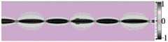
图1为本发明多频段波导元器件的结构示意图;1 is a schematic structural diagram of a multi-band waveguide component of the present invention;
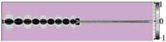
图2为本发明谐振器的结构示意图;Fig. 2 is the structural representation of the resonator of the present invention;
图3为本发明多频段波导元器件的S11参数曲线随PIN二极管导通特性的变化图;Fig. 3 is the variation diagram of theS11 parameter curve of the multi-band waveguide component of the present invention with the conduction characteristic of the PIN diode;
图4为本发明多频段波导元器件的S12参数曲线随PIN二极管导通特性的变化图;FIG. 4 is a graph showing the variation of theS12 parameter curve of the multi-band waveguide component according to the conduction characteristic of the PIN diode;
图5为本发明多频段波导元器件的加载第一PIN二极管和第二PIN二极管状态下的群时延特性曲线图;FIG. 5 is a graph showing the group delay characteristics of the multi-band waveguide components of the present invention when the first PIN diode and the second PIN diode are loaded;
图6为本发明多频段波导元器件在工作频率为3GHz,无第一PIN二极管和第二PIN二极管加载状态下的电场分布图;Fig. 6 is the electric field distribution diagram of the multi-band waveguide component of the present invention when the operating frequency is 3GHz, and the first PIN diode and the second PIN diode are not loaded;
图7为本发明多频段波导元器件在工作频率为9.7GHz,无第一PIN二极管和第二PIN二极管加载状态下的电场分布图;FIG. 7 is an electric field distribution diagram of the multi-band waveguide component of the present invention when the operating frequency is 9.7 GHz and no first PIN diode and second PIN diode are loaded;
图8为本发明多频段波导元器件在工作频率为3GHz,第一PIN二极管加载状态下的电场分布图;8 is an electric field distribution diagram of the multi-band waveguide component of the present invention when the operating frequency is 3 GHz and the first PIN diode is loaded;
图9为本发明多频段波导元器件在工作频率为9.7GHz,第一PIN二极管加载状态下的电场分布图;Fig. 9 is the electric field distribution diagram of the multi-band waveguide component of the present invention when the operating frequency is 9.7 GHz and the first PIN diode is loaded;
图10为本发明多频段波导元器件在工作频率为6.7GHz,第一PIN二极管和第二PIN二极管同时加载状态下的电场分布图;Fig. 10 is an electric field distribution diagram of the multi-band waveguide component of the present invention when the operating frequency is 6.7 GHz and the first PIN diode and the second PIN diode are simultaneously loaded;
图11为本发明多频段波导元器件在工作频率为21.8GHz,第一PIN二极管和第二PIN二极管同时加载状态下的电场分布图。11 is an electric field distribution diagram of the multi-band waveguide component of the present invention when the operating frequency is 21.8 GHz and the first PIN diode and the second PIN diode are simultaneously loaded.
附图中,各标号所代表的部件列表如下:In the accompanying drawings, the list of components represented by each number is as follows:
1、介质板,2、传输段,3、过渡段,4、人工表面等离激元段,5、第一矩形槽,6、第二矩形槽,7、谐振器,8、焊盘,9、高阻线,10、第一PIN二极管,11、电容,12、第三矩形槽,13、第二PIN二极管。1. Dielectric plate, 2. Transmission section, 3. Transition section, 4. Artificial surface plasmon section, 5. First rectangular slot, 6. Second rectangular slot, 7. Resonator, 8. Pad, 9 , High resistance wire, 10, First PIN diode, 11, Capacitor, 12, Third rectangular slot, 13, Second PIN diode.
具体实施方式Detailed ways
以下结合附图对本发明的原理和特征进行描述,所举实例只用于解释本发明,并非用于限定本发明的范围。The principles and features of the present invention will be described below with reference to the accompanying drawings. The examples are only used to explain the present invention, but not to limit the scope of the present invention.
实施例Example
如图1-图2所示,本实施例提供一种实时可控的多频段波导元器件,包括:介质板1;金属微带,谐振器7和第一PIN二极管10。As shown in FIGS. 1-2 , this embodiment provides a real-time controllable multi-band waveguide component, including: a
金属微带固定连接在介质板1的一面上,金属微带铺设在介质板1上,金属微带的中部设有人工表面等离激元结构。谐振器7位于金属微带的中部两侧,谐振器7与介质板1的一面固定连接。第一PIN二极管10一端与谐振器7连接,另一端与金属微带的中部连接,电流从谐振器7经第一PIN二极管10进入到金属微带中。其中谐振器7为两个,两个谐振器7相对设置在金属微带的两侧。The metal microstrip is fixedly connected on one side of the
本实施例的技术方案可产生如下效果,通过设置的第一PIN二极管10来连通谐振器7和金属微带,使得能在传输曲线上实时引入传输零点,使得谐振频率实时可控,实时调节波导传输曲线上的传输零点。通过在金属微带上设置的人工表面等离激元结构,其具有微波截至模式,从而使得本波导元器件可以在三种不同的微波频段工作,实现多功能化。The technical solution of this embodiment can produce the following effects: the
此外,人工表面等离激元结构能让电磁场在平面界面传输时被束缚,从而大大降低了多条传输线传输时因间距太小而出现的电磁干扰,使得波导元器件抗干扰能力大大增强,同时也增强了本发明用于高密度微波集成电路中工作时的稳定性。In addition, the artificial surface plasmon structure can make the electromagnetic field bound during the transmission of the plane interface, thus greatly reducing the electromagnetic interference caused by the too small distance between multiple transmission lines, which greatly enhances the anti-interference ability of the waveguide components. It also enhances the stability of the present invention when used in high-density microwave integrated circuits.
不仅如此,因抗电磁干扰能力大大增强,本实施例还能减小微波集成电路的金属微带间的间距以实现器件的小型化,因而能更好地适应当今大规模微波集成电路的发展。Not only that, because the anti-electromagnetic interference capability is greatly enhanced, the present embodiment can also reduce the spacing between the metal microstrips of the microwave integrated circuit to realize the miniaturization of the device, thus better adapting to the development of today's large-scale microwave integrated circuits.
优选地,本实施例中,谐振器7上设有焊盘8,焊盘8与谐振器7之间设有高阻线9,高阻线9的两端分别与焊盘8和谐振器7连接。其中焊盘8用于与外部电压连接,用于施加电压。通过高阻线9使得交流信号无法到达直流电压,不会对电源影响。Preferably, in this embodiment, a
优选地,本实施例中,金属微带的中部设有电容11,第一PIN二极管10的另一端与电容11连接。其中电容11与第一PIN二极管10配套设置,通过设置的电容11与第一PIN二极管10串接,使直流偏置电压无法到达主金属微带,不会对交流信号构成干扰。Preferably, in this embodiment, a capacitor 11 is provided in the middle of the metal microstrip, and the other end of the
优选地,本实施例中,谐振器7包括多个谐振单元,多个谐振单元并列设置,多个谐振单元上均设有第一矩形槽5,第一矩形槽5朝向金属微带。从而实现电磁场传输时产生谐振效果。其中谐振单元为3个。Preferably, in this embodiment, the
优选地,本实施例中,多个谐振单元之间均设有第二PIN二极管13,相邻两个谐振单元通过对应第二PIN二极管13连接,电流通过第二PIN二极管13向第一PIN二极管10流动。从而使谐振频率实时可控,实时调节波导传输曲线上的传输零点,控制效果更好。Preferably, in this embodiment,
优选地,本实施例中,金属微带包括人工表面等离激元段4、两个过渡段3和两个传输段2,两个过渡段3的一端分别与人工表面等离激元段4的两端连接,两个过渡段3的另一端分别与两个传输段2的一端连接,两个传输段2的另一端与介质板1的两边的边缘齐平。Preferably, in this embodiment, the metal microstrip includes an artificial
其中两个过渡段3和两个传输段2均以人工表面等离激元段4对称设置。其中传输段2用于电磁场输入和电磁场输出,其中过渡段3能够实现电磁场平稳过渡。The two transition sections 3 and the two
优选地,本实施例中,两个过渡段3的两侧边上均设有多个第二矩形槽6,多个第二矩形槽6沿对应过渡段3的长度方向并列设置。其中通过设置的第二矩形槽6实现对微波的收束,同时能够防止相互之间的电磁干扰。Preferably, in this embodiment, a plurality of second
优选地,本实施例中,人工表面等离激元段4的两侧上均设有多个第三矩形槽12,多个第三矩形槽12沿对应人工表面等离激元段4的长度方向并列设置。通过第三矩形槽12形成人工表面等离激元结构,通过第三矩形槽12成周期性的阵列排布,从而具有微波截止模式。Preferably, in this embodiment, multiple third
另外还能通过调节第二矩形槽6和第三矩形槽12的几何尺寸来调控微波传输线的传输零点频率和电磁场分布,同时调整电磁波的束缚效果。In addition, by adjusting the geometric dimensions of the second
优选地,本实施例中,第二矩形槽6的槽底沿过渡段3朝人工表面等离激元段4方向逐渐向轴线倾斜。第二矩形槽6的槽底深度沿过渡段3朝人工表面等离激元段4方向逐渐增加。从而使得电磁场传播的过渡最平稳。Preferably, in this embodiment, the groove bottom of the second
优选地,本实施例中,人工表面等离激元段4的长度为30~60mm;第三矩形槽12的深度为0.1~10.0mm,宽度为0.25~5mm。过渡段3的长度为10-30mm。其中图1中,L1为传输段2,L2为过渡段3,L3为人工表面等离激元段4。其中第二矩形槽6的深度为0.1~10.0mm,宽度为0.25~5mm。Preferably, in this embodiment, the length of the artificial
优选地,本实施例中,介质板1的厚度为0.05~1.5mm,介质板1的另一面上固定设有金属地。Preferably, in this embodiment, the thickness of the
工作原理:准TEM模式的电磁场由左边的传输段2传输到过渡段3,在过渡段3中逐渐渐变为SSPPs模式的电磁场,且在过渡段3中准TEM模式和SSPPs模式的电磁场共存,当进入到人工表面等离激元段4时,完全转化为SSPPs模式的电磁场,并在人工表面等离激元段4进行传输,当连接第一PIN二极管10,电磁场在第一PIN二极管10处连接谐振器7,谐振器7的谐振在人工等离激元段产生传输零点,阻止电磁场沿金属微带的输出。当第二PIN二极管13接通时,谐振器7中的谐振单元增多,谐振频率降低,从而实时调控传输零点的位置及波导的带宽。电磁场在传输段2上传播时,传输段2内电磁场的模式为准TEM模式,该模式电磁场被束缚在传输段2与金属地间的介质板1内;电磁场在过渡段3传播时,过渡段3内准TEM模式与SSPPs模式共存,其中准TEM模式电磁场被束缚在过渡段3与金属地间的介质板1内,SSPPs模式电磁场被束缚在第二矩形槽6周围;在人工表面等离激元段4进行传播时,该段内电磁场为SSPPs模式,该模式电磁场被束缚在第三矩形槽12周围,可有效增加波导的电磁抗干扰能力。Working principle: The electromagnetic field of the quasi-TEM mode is transmitted from the
以下为采用上述实施例进行具体测量的情况。The following is the case where the above-mentioned embodiment is used to carry out the specific measurement.
根据上述实施例制备一个多频段波导元器件,它各部分几何参数如表1所示。According to the above embodiment, a multi-band waveguide component is prepared, and the geometric parameters of each part are shown in Table 1.
表1Table 1


其中周期为两个相邻矩形槽之间的距离。where the period is the distance between two adjacent rectangular slots.
该样品的介质板1采用介电常数为2.65的基片,对该多频段波导元器件散射参数采用有限积分的计算结果如图3-4所示。The
图中S11为滤波器反射系数,S21为滤波器传输系数,列举了该多频段波导元器件工作频段中的传输反射特性,其中无PIN二极管加载时多频段波导元器件为低通段,其-3dB通带范围为0~27.5GHz,该带内反射系数均小于-11dB,多频段波导元器件在该通带内插损很小,大于-0.9dB,纹波抖动小于0.87dB。In the figure, S11 is the reflection coefficient of the filter, and S21 is the transmission coefficient of the filter. The transmission and reflection characteristics of the multi-band waveguide components in the working frequency band are listed. When no PIN diode is loaded, the multi-band waveguide components are in the low-pass section. The -3dB passband range is 0 to 27.5GHz, and the reflection coefficient in this band is less than -11dB. The multi-band waveguide components have very small insertion loss in this passband, greater than -0.9dB, and ripple jitter less than 0.87dB.
当加载第一PIN二极管10后,多频段波导元器件引入两个传输零点变为三波段,其-3dB频带范围为0~3.64GHz,13.7~22.5GHz以及28.7~31.6GHz,多频段波导元器件在通带内最低插损小于-0.27dB。When the
当同时加载第一PIN二极管10和第二PIN二极管13时,带通内的传输零点发生实时移动,但带内反射系数及纹波抖动无明显变化,如图3-4所示。When the
当同时加载第一PIN二极管10和第二PIN二极管13时,测量多频段波导元器件的群延时,具体如图5所示。When the
由图5可知,该频段内群时延小于1.8ns,信号失真小,说明多频段波导元器件传输特性好,带外抑制优。而且上述带通的带宽特性可以由多频段波导元器件的第二矩形槽6和第三矩形槽12的深度改变来方便的调节。使该多频段波导元器件具备多种通讯制式的工作能力,能有效减少通讯系统中器件个数,缩小系统的体积。It can be seen from Figure 5 that the group delay in this frequency band is less than 1.8ns, and the signal distortion is small, indicating that the multi-band waveguide components have good transmission characteristics and excellent out-of-band suppression. Moreover, the bandwidth characteristics of the above-mentioned band pass can be conveniently adjusted by changing the depths of the second
对多频段波导元器件工作于3.0GHz时的表面电场分布做计算,结果如图6所示。The surface electric field distribution of the multi-band waveguide components operating at 3.0GHz is calculated, and the results are shown in Figure 6.
对多频段波导元器件工作于9.7GHz阻带时的表面电场分布做计算,结果如图7所示。此时,电磁场能量均能顺利通过波导。The surface electric field distribution of the multi-band waveguide components operating in the 9.7GHz stopband is calculated, and the results are shown in Figure 7. At this time, the electromagnetic field energy can pass through the waveguide smoothly.
对多频段波导元器件加载第一PIN二极管10与谐振器7连通,工作于3.0GHz时的表面电场分布做计算,结果如图8所示。The multi-band waveguide component is loaded with the
对多频段波导元器件加载第一PIN二极管10与谐振器7连通,工作于9.7GHz时的表面电场分布做计算,结果如图9所示。The multi-band waveguide components are loaded with the
由图9得知,样品在通带内由于谐振器7的谐振实时引入传输零点。电场能量由波导输入端口输入后,在谐振器7处发生谐振,无法传播输出。It is known from FIG. 9 that the sample introduces a transmission zero in real time due to the resonance of the
图10为第一PIN二极管10和第二PIN二极管13同时加载时,在工作频率为6.7GHz和21.8GHz的工作状态下,多频段波导元器件的电场分布图。由图可知,第二PIN二极管13可实时调控传输零点,从而实时改变多频段波导元器件的带宽和工作范围。多频段波导元器件在通带内工作时,电场可以由一个传输段2通过人工表面等离激元段4传输顺利传输到另一个传输段2,且电场能量被局域于第二矩形槽6和第三矩形槽12的周围,向四周扩散很小,这使得波导抗电磁干扰的能力大大加强。10 is a diagram showing the electric field distribution of the multi-band waveguide component when the
在本发明的描述中,需要理解的是,术语“中心”、“长度”、“上”、“下”、“前”、“后”、“左”、“右”、“竖直”、“水平”、“顶”、“内”、“外”、“周侧”、“周向”等指示的方位或位置关系为基于附图所示的方位或位置关系,仅是为了便于描述本发明和简化描述,而不是指示或暗示所指的装置或元件必须具有特定的方位、以特定的方位构造和操作,因此不能理解为对本发明的限制。In the description of the present invention, it should be understood that the terms "center", "length", "upper", "lower", "front", "rear", "left", "right", "vertical", The orientation or positional relationship indicated by "horizontal", "top", "inner", "outer", "circumferential side", "circumferential direction", etc. is based on the orientation or positional relationship shown in the accompanying drawings, and is only for the convenience of describing the present invention. The invention and simplified description do not indicate or imply that the device or element referred to must have a particular orientation, be constructed and operate in a particular orientation, and therefore should not be construed as limiting the invention.
在本发明的描述中,“多个”的含义是至少两个,例如两个,三个等,除非另有明确具体的限定。In the description of the present invention, "plurality" means at least two, such as two, three, etc., unless otherwise expressly and specifically defined.
在本发明中,除非另有明确的规定和限定,术语“安装”、“相连”、“连接”、“固定”等术语应做广义理解,例如,可以是固定连接,也可以是可拆卸连接,或成一体;可以是机械连接,也可以是电连接;可以是直接相连,也可以通过中间媒介间接相连,可以是两个元件内部的连通或两个元件的相互作用关系,除非另有明确的限定。对于本领域的普通技术人员而言,可以根据具体情况理解上述术语在本发明中的具体含义。In the present invention, unless otherwise expressly specified and limited, the terms "installed", "connected", "connected", "fixed" and other terms should be understood in a broad sense, for example, it may be a fixed connection or a detachable connection , or integrated; it can be a mechanical connection or an electrical connection; it can be directly connected or indirectly connected through an intermediate medium, it can be the internal connection of two elements or the interaction relationship between the two elements, unless otherwise specified limit. For those of ordinary skill in the art, the specific meanings of the above terms in the present invention can be understood according to specific situations.
在本说明书的描述中,参考术语“一个实施例”、“一些实施例”、“示例”、“具体示例”、或“一些示例”等的描述意指结合该实施例或示例描述的具体特征、结构、材料或者特点包含于本发明的至少一个实施例或示例中。在本说明书中,对上述术语的示意性表述不必须针对的是相同的实施例或示例。而且,描述的具体特征、结构、材料或者特点可以在任一个或多个实施例或示例中以合适的方式结合。此外,在不相互矛盾的情况下,本领域的技术人员可以将本说明书中描述的不同实施例或示例以及不同实施例或示例的特征进行结合和组合。In the description of this specification, description with reference to the terms "one embodiment," "some embodiments," "example," "specific example," or "some examples", etc., mean specific features described in connection with the embodiment or example , structure, material or feature is included in at least one embodiment or example of the present invention. In this specification, schematic representations of the above terms are not necessarily directed to the same embodiment or example. Furthermore, the particular features, structures, materials or characteristics described may be combined in any suitable manner in any one or more embodiments or examples. Furthermore, those skilled in the art may combine and combine the different embodiments or examples described in this specification, as well as the features of the different embodiments or examples, without conflicting each other.
以上所述仅为本发明的较佳实施例,并不用以限制本发明,凡在本发明的精神和原则之内,所作的任何修改、等同替换、改进等,均应包含在本发明的保护范围之内。The above are only preferred embodiments of the present invention and are not intended to limit the present invention. Any modifications, equivalent replacements, improvements, etc. made within the spirit and principles of the present invention shall be included in the protection of the present invention. within the range.
Claims (10)
Translated fromChinesePriority Applications (1)
| Application Number | Priority Date | Filing Date | Title |
|---|---|---|---|
| CN202010667522.2ACN111834718B (en) | 2020-07-13 | 2020-07-13 | Real-time controllable multi-band waveguide component |
Applications Claiming Priority (1)
| Application Number | Priority Date | Filing Date | Title |
|---|---|---|---|
| CN202010667522.2ACN111834718B (en) | 2020-07-13 | 2020-07-13 | Real-time controllable multi-band waveguide component |
Publications (2)
| Publication Number | Publication Date |
|---|---|
| CN111834718Atrue CN111834718A (en) | 2020-10-27 |
| CN111834718B CN111834718B (en) | 2024-09-10 |
Family
ID=72900588
Family Applications (1)
| Application Number | Title | Priority Date | Filing Date |
|---|---|---|---|
| CN202010667522.2AActiveCN111834718B (en) | 2020-07-13 | 2020-07-13 | Real-time controllable multi-band waveguide component |
Country Status (1)
| Country | Link |
|---|---|
| CN (1) | CN111834718B (en) |
Citations (4)
| Publication number | Priority date | Publication date | Assignee | Title |
|---|---|---|---|---|
| US7773228B1 (en)* | 2007-08-15 | 2010-08-10 | Itn Energy Systems, Inc. | Surface plasmon noncontact electric field sensors and related methods |
| US20130301983A1 (en)* | 2012-05-08 | 2013-11-14 | Pinaki Mazumder | Dynamic Terahertz Switching Device Comprising Sub-wavelength Corrugated Waveguides and Cavity that Utilizes Resonance and Absorption for Attaining On and Off states |
| CN104810579A (en)* | 2015-05-12 | 2015-07-29 | 中国矿业大学 | Tunable bandstop filter based on artificial surface plasmon |
| CN212303864U (en)* | 2020-07-13 | 2021-01-05 | 贵州民族大学 | A real-time controllable multi-band waveguide component |
- 2020
- 2020-07-13CNCN202010667522.2Apatent/CN111834718B/enactiveActive
Patent Citations (4)
| Publication number | Priority date | Publication date | Assignee | Title |
|---|---|---|---|---|
| US7773228B1 (en)* | 2007-08-15 | 2010-08-10 | Itn Energy Systems, Inc. | Surface plasmon noncontact electric field sensors and related methods |
| US20130301983A1 (en)* | 2012-05-08 | 2013-11-14 | Pinaki Mazumder | Dynamic Terahertz Switching Device Comprising Sub-wavelength Corrugated Waveguides and Cavity that Utilizes Resonance and Absorption for Attaining On and Off states |
| CN104810579A (en)* | 2015-05-12 | 2015-07-29 | 中国矿业大学 | Tunable bandstop filter based on artificial surface plasmon |
| CN212303864U (en)* | 2020-07-13 | 2021-01-05 | 贵州民族大学 | A real-time controllable multi-band waveguide component |
Non-Patent Citations (2)
| Title |
|---|
| HAOTIAN LING 等: "Reconfigurable Spoof Surface Plasmon Polariton Band-stop Filter with Monolithic Schottky Diodes", 《2019 PHOTONICS & ELECTROMAGNETICS RESEARCH SYMPOSIUM - FALL (PIERS - FALL)》, 5 March 2020 (2020-03-05), pages 337 - 343* |
| 娄菁 等: "基于谐振耦合和人工表面等离激元的可调控频率选择铁电厚膜移相器", 《电子元件与材料》, vol. 38, no. 4, 19 April 2019 (2019-04-19), pages 101 - 105* |
Also Published As
| Publication number | Publication date |
|---|---|
| CN111834718B (en) | 2024-09-10 |
Similar Documents
| Publication | Publication Date | Title |
|---|---|---|
| CN205666315U (en) | Be used for W wave band waveguide - microstrip probe converter | |
| CN107819180B (en) | Substrate integrated waveguide device and substrate integrated waveguide filter | |
| CN113300065B (en) | Mixed mode band-pass filter based on triangular substrate integrated waveguide | |
| CN108520996B (en) | Substrate integrated waveguide attenuator with surface adhered with resistor | |
| CN105977595A (en) | Terminal connection feed-backward type rectangular waveguide-microstrip transition device | |
| CN108172958A (en) | A Periodic Slow Wave Transmission Line Unit Based on Coplanar Waveguide | |
| CN107732383B (en) | Dual-band microwave band-pass filter | |
| CN113036334B (en) | A Bandwidth Controllable Millimeter-Wave Filter Based on Plasmons | |
| CN111969286B (en) | Waveguide component based on composite thin film resonator | |
| CN110429362B (en) | Reconfigurable filter based on T-shaped resonator | |
| CN111864321A (en) | A Balanced Dual-pass Band Filter Based on Branch Loaded Slotline Resonator | |
| CN108736120B (en) | A half-mode substrate integrated waveguide attenuator based on surface mount resistance | |
| US10673111B2 (en) | Filtering unit and filter | |
| CN212303864U (en) | A real-time controllable multi-band waveguide component | |
| CN105896007A (en) | Microwave band-pass filter | |
| CN109244609B (en) | A kind of square groove structure microwave filter with dual band operation characteristic | |
| CN104167578B (en) | Substrate integration wave-guide band pass filter | |
| CN112072223A (en) | Negative slope frequency dependence coupling structure and cross-coupling SIW band-pass filter | |
| CN111834718A (en) | A real-time controllable multi-band waveguide component | |
| CN214313472U (en) | A real-time controllable waveguide structure based on ferroelectric films | |
| CN112864558B (en) | Real-time controllable waveguide structure based on ferroelectric film | |
| CN207009620U (en) | A Miniaturized Microwave Bandpass Filter | |
| CN106848508A (en) | A kind of wide-band microwave bandpass filter | |
| CN109755706B (en) | High out-of-band rejection electromagnetic shunt coupling filter | |
| CN210805968U (en) | A Y-type microwave demultiplexing structure and microwave demultiplexer |
Legal Events
| Date | Code | Title | Description |
|---|---|---|---|
| PB01 | Publication | ||
| PB01 | Publication | ||
| SE01 | Entry into force of request for substantive examination | ||
| SE01 | Entry into force of request for substantive examination | ||
| GR01 | Patent grant | ||
| GR01 | Patent grant |