CN111818241A - Camera module and molded photosensitive component, manufacturing method thereof, and electronic device - Google Patents
Camera module and molded photosensitive component, manufacturing method thereof, and electronic deviceDownload PDFInfo
- Publication number
- CN111818241A CN111818241ACN201910292636.0ACN201910292636ACN111818241ACN 111818241 ACN111818241 ACN 111818241ACN 201910292636 ACN201910292636 ACN 201910292636ACN 111818241 ACN111818241 ACN 111818241A
- Authority
- CN
- China
- Prior art keywords
- molding
- molding part
- camera module
- molded
- base
- Prior art date
- Legal status (The legal status is an assumption and is not a legal conclusion. Google has not performed a legal analysis and makes no representation as to the accuracy of the status listed.)
- Granted
Links
- 238000004519manufacturing processMethods0.000titleclaimsabstractdescription51
- 238000000465mouldingMethods0.000claimsabstractdescription779
- 230000003287optical effectEffects0.000claimsabstractdescription95
- 238000003384imaging methodMethods0.000claimsabstractdescription88
- 239000000853adhesiveSubstances0.000claimsdescription72
- 230000001070adhesive effectEffects0.000claimsdescription72
- 239000012790adhesive layerSubstances0.000claimsdescription40
- 238000000034methodMethods0.000claimsdescription29
- 239000003292glueSubstances0.000claimsdescription23
- 230000003014reinforcing effectEffects0.000claimsdescription20
- 238000001723curingMethods0.000claimsdescription14
- 230000002787reinforcementEffects0.000claimsdescription13
- 230000002093peripheral effectEffects0.000claimsdescription10
- 238000013007heat curingMethods0.000claimsdescription2
- 230000000712assemblyEffects0.000claims1
- 238000000429assemblyMethods0.000claims1
- 239000003795chemical substances by applicationSubstances0.000claims1
- 238000007373indentationMethods0.000claims1
- 230000007704transitionEffects0.000description26
- 230000008569processEffects0.000description18
- 238000009434installationMethods0.000description12
- 239000000463materialSubstances0.000description5
- 230000002411adverseEffects0.000description4
- 230000009286beneficial effectEffects0.000description4
- 238000010586diagramMethods0.000description4
- 239000000428dustSubstances0.000description4
- 230000000694effectsEffects0.000description4
- 239000010410layerSubstances0.000description4
- 230000000903blocking effectEffects0.000description3
- 230000008859changeEffects0.000description3
- 238000010438heat treatmentMethods0.000description3
- 238000000576coating methodMethods0.000description2
- 238000004891communicationMethods0.000description2
- 238000001816coolingMethods0.000description2
- 238000011161developmentMethods0.000description2
- 238000005516engineering processMethods0.000description2
- 238000012858packaging processMethods0.000description2
- 238000013459approachMethods0.000description1
- 239000011248coating agentSubstances0.000description1
- 238000011109contaminationMethods0.000description1
- 238000005336crackingMethods0.000description1
- 238000009826distributionMethods0.000description1
- 230000003028elevating effectEffects0.000description1
- 230000002708enhancing effectEffects0.000description1
- 239000007888film coatingSubstances0.000description1
- 238000009501film coatingMethods0.000description1
- 238000001914filtrationMethods0.000description1
- 238000012986modificationMethods0.000description1
- 230000004048modificationEffects0.000description1
- 239000012778molding materialSubstances0.000description1
- 238000012634optical imagingMethods0.000description1
- 230000009467reductionEffects0.000description1
- 230000003595spectral effectEffects0.000description1
- 238000005728strengtheningMethods0.000description1
Images


Classifications
- H—ELECTRICITY
- H04—ELECTRIC COMMUNICATION TECHNIQUE
- H04N—PICTORIAL COMMUNICATION, e.g. TELEVISION
- H04N23/00—Cameras or camera modules comprising electronic image sensors; Control thereof
- H04N23/50—Constructional details
- H04N23/54—Mounting of pick-up tubes, electronic image sensors, deviation or focusing coils
- B—PERFORMING OPERATIONS; TRANSPORTING
- B29—WORKING OF PLASTICS; WORKING OF SUBSTANCES IN A PLASTIC STATE IN GENERAL
- B29C—SHAPING OR JOINING OF PLASTICS; SHAPING OF MATERIAL IN A PLASTIC STATE, NOT OTHERWISE PROVIDED FOR; AFTER-TREATMENT OF THE SHAPED PRODUCTS, e.g. REPAIRING
- B29C65/00—Joining or sealing of preformed parts, e.g. welding of plastics materials; Apparatus therefor
- B29C65/48—Joining or sealing of preformed parts, e.g. welding of plastics materials; Apparatus therefor using adhesives, i.e. using supplementary joining material; solvent bonding
- H—ELECTRICITY
- H04—ELECTRIC COMMUNICATION TECHNIQUE
- H04N—PICTORIAL COMMUNICATION, e.g. TELEVISION
- H04N23/00—Cameras or camera modules comprising electronic image sensors; Control thereof
- H04N23/50—Constructional details
- H—ELECTRICITY
- H04—ELECTRIC COMMUNICATION TECHNIQUE
- H04N—PICTORIAL COMMUNICATION, e.g. TELEVISION
- H04N23/00—Cameras or camera modules comprising electronic image sensors; Control thereof
- H04N23/50—Constructional details
- H04N23/55—Optical parts specially adapted for electronic image sensors; Mounting thereof
- H—ELECTRICITY
- H04—ELECTRIC COMMUNICATION TECHNIQUE
- H04N—PICTORIAL COMMUNICATION, e.g. TELEVISION
- H04N23/00—Cameras or camera modules comprising electronic image sensors; Control thereof
- H04N23/57—Mechanical or electrical details of cameras or camera modules specially adapted for being embedded in other devices
Landscapes
- Engineering & Computer Science (AREA)
- Multimedia (AREA)
- Signal Processing (AREA)
- Mechanical Engineering (AREA)
- Transforming Light Signals Into Electric Signals (AREA)
- Studio Devices (AREA)
Abstract
Translated fromChinese
Description
Translated fromChinese技术领域technical field
本发明涉及光学成像技术领域,特别是涉及一种摄像模组和模塑感光组件及其制造方法以及电子设备。The invention relates to the technical field of optical imaging, in particular to a camera module and a molded photosensitive component, a manufacturing method thereof, and an electronic device.
背景技术Background technique
近年来,电子产品、智能设备等越来越多地朝向轻薄化、小型化的方向发展,电子产品、智能设备这种发展趋势对作为电子产品、智能设备的标准配置之一的摄像模组的尺寸提出了更加苛刻的要求。在此要求下,模塑工艺和IOM(IR on Molding,滤光片在模塑上)工艺逐渐被应用于摄像模组的封装工艺中,首先通过模塑工艺封装成像组件以形成模塑基座,之后再将滤光片直接贴附于模塑基座上,以组装成模塑感光组件,从而大幅地减少感光组件的厚度,进而缩小摄像模组的整体尺寸。In recent years, electronic products, smart devices, etc. have been increasingly developed in the direction of thinning and miniaturization. The development trend of electronic products and smart devices has a great impact on the camera module, which is one of the standard configurations of electronic products and smart devices. Dimensions impose more stringent requirements. Under this requirement, the molding process and the IOM (IR on Molding, filter on molding) process are gradually applied to the packaging process of the camera module. First, the imaging component is packaged through the molding process to form a molding base. , and then directly attach the filter to the molding base to assemble a molded photosensitive component, thereby greatly reducing the thickness of the photosensitive component, thereby reducing the overall size of the camera module.
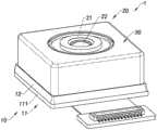
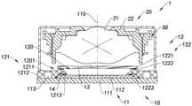
例如,如图1所示,现有的摄像模组1P通常包括一光学镜头2P和一模塑感光组件3P,其中该模塑感光组件3P包括一成像组件31P、一模塑基座32P以及一滤光片33P,其中该模塑基座32P在模塑成型后包覆该成像组件31P的一部分,并且该模塑基座32P的内部向下凹陷以形成一凹槽35P,其中该滤光片33P通过胶水被直接贴附至该模塑基座32P的该凹槽35P内,并在胶水固化后形成将该滤光片33P与该模塑基座32P粘接的胶层34P,以组装成该模塑感光组件3P。这样现有的摄像模组1P在不需要镜座的基础上,只需将该光学镜头2P直接安装至该模塑基座32P的顶表面就能够完成模组组装,以便降低摄像模组的整体尺寸。与此同时,由于该滤光片33P被贴附于该模塑基座32P的凹槽35P内,因此该滤光片33P与该成像组件31P的感光芯片311P之间的距离得以进一步减小,有助于进一步降低摄像模组的高度。For example, as shown in FIG. 1 , an existing
然而,如图1所示,受限于模塑工艺中的覆膜(film),该模塑基座32P中该凹槽35P的拐角处(即该模塑基座32P上贴附该滤光片33P的部位与安装该光学镜头2P的部分之间的连接处)并非直角,而是存在一定的过渡弧面351P,导致该模塑基座32P难以为该滤光片33P提供一平整的贴附面。因此,在贴附该滤光片33P时不得不避让该模塑基座32P中该凹槽35P的该过渡弧面351P,以确保该滤光片33P被贴附在平整的平面上。但这样就会导致该滤光片33P与该模塑基座32P之间的贴附面积变小,即该模塑基座32P为该滤光片33P提供的底部支撑面积变小,容易降低该滤光片33P与该模塑基座32P之间的连接强度,进而影响摄像模组的可靠性。However, as shown in FIG. 1 , limited by the film in the molding process, the corners of the
发明内容SUMMARY OF THE INVENTION
本发明的一目的在于提供一种摄像模组和模塑感光组件及其制造方法以及电子设备,其能够通过垫高模塑基座上贴附滤光构件的部位,以消除所述模塑基座上的过渡弧面对所述贴附滤光构件产生的不利影响。One object of the present invention is to provide a camera module and a molded photosensitive assembly, a manufacturing method thereof, and an electronic device, which can eliminate the molding base by elevating the part where the filter member is attached on the molding base. The transition arc on the seat has an adverse effect on the attached filter member.
本发明的另一目的在于提供一种摄像模组和模塑感光组件及其制造方法以及电子设备,其能够在贴附所述滤光构件时无需避让所述模塑基座上的过渡弧面,以便增大所述滤光构件与所述模塑基座之间的贴附面积,有助于提高所述摄像模组的可靠性。Another object of the present invention is to provide a camera module and a molded photosensitive assembly, a manufacturing method thereof, and an electronic device, which can avoid the transition arc surface on the molding base when attaching the filter member. , so as to increase the attachment area between the filter member and the molding base, and help improve the reliability of the camera module.
本发明的另一目的在于提供一种摄像模组和模塑感光组件及其制造方法以及电子设备,其中,在本发明的一实施例中,通过对成型模具的上模具进行设计,以在第二模塑部和第三模塑部之间形成间隙,使得所述滤光构件无需避让所述模塑基座上的过渡弧面。Another object of the present invention is to provide a camera module and a molded photosensitive component, a manufacturing method thereof, and an electronic device, wherein, in an embodiment of the present invention, the upper mold of the molding mold is designed to A gap is formed between the second molding part and the third molding part, so that the filter member does not need to avoid the transition arc surface on the molding base.
本发明的另一目的在于提供一种摄像模组和模塑感光组件及其制造方法以及电子设备,其中,在本发明的一实施例中,所述模塑感光组件的所述模塑基座的第二模塑部一体地形成于所述模塑基座的第一模塑部,以通过所述第二模塑部的第二上表面为所述滤光构件提供一平整贴附面,便于确保所述滤光构件的贴附平整度。Another object of the present invention is to provide a camera module and a molded photosensitive component, a manufacturing method thereof, and an electronic device, wherein, in an embodiment of the present invention, the molding base of the molded photosensitive component The second molding portion is integrally formed on the first molding portion of the molding base, so as to provide a flat attachment surface for the filter member through the second upper surface of the second molding portion, It is convenient to ensure the flatness of attachment of the filter member.
本发明的另一目的在于提供一种摄像模组和模塑感光组件及其制造方法以及电子设备,其中,在本发明的一实施例中,所述模塑感光组件的所述模塑基座的第三模塑部一体地形成于所述第一模塑部,以包覆所述模塑感光组件的线路板上的电子元器件,有助于降低所述第一模塑部的厚度,进而降低所述摄像模组的高度。Another object of the present invention is to provide a camera module and a molded photosensitive component, a manufacturing method thereof, and an electronic device, wherein, in an embodiment of the present invention, the molding base of the molded photosensitive component The third molding part is integrally formed on the first molding part to cover the electronic components on the circuit board of the molding photosensitive component, which helps to reduce the thickness of the first molding part, Further, the height of the camera module is reduced.
本发明的另一目的在于提供一种摄像模组和模塑感光组件及其制造方法以及电子设备,其中,在本发明的一实施例中,所述模塑感光组件的所述模组基座的所述第二模塑部与第三模塑部间隔设置,以在所述第二模塑部和所述第三模塑部之间预留一外空间,使得所述滤光元件的边缘尽可能靠近所述第三模塑部,而不需要避让所述第三模塑部与所述第一模塑部之间的过渡弧面,有助于增大所述滤光元件的底部支撑面积,从而增强所述滤光元件的贴附可靠性。Another object of the present invention is to provide a camera module and a molded photosensitive component, a manufacturing method thereof, and an electronic device, wherein, in an embodiment of the present invention, the module base of the molded photosensitive component The second molding part and the third molding part are spaced apart to reserve an outer space between the second molding part and the third molding part, so that the edge of the filter element As close as possible to the third molding part without avoiding the transition arc between the third molding part and the first molding part, it helps to increase the bottom support of the filter element area, thereby enhancing the attachment reliability of the filter element.
本发明的另一目的在于提供一种摄像模组和模塑感光组件及其制造方法以及电子设备,其中,在本发明的一实施例中,所述模塑感光组件的所述模组基座的所述第二模塑部能够确保所述滤光元件被贴附在平整的平面上,而不需要避让所述第三模塑部与所述第一模塑部之间的过渡弧面,有助于提高所述摄像模组的组装质量。Another object of the present invention is to provide a camera module and a molded photosensitive component, a manufacturing method thereof, and an electronic device, wherein, in an embodiment of the present invention, the module base of the molded photosensitive component The second molding part can ensure that the filter element is attached to a flat plane without avoiding the transition arc between the third molding part and the first molding part, This helps to improve the assembly quality of the camera module.
本发明的另一目的在于提供一种摄像模组和模塑感光组件及其制造方法以及电子设备,其中,在本发明的一实施例中,所述模塑基座的所述第二模塑部易于设置缺口,以在贴附所述滤光构件的过程中形成逃气孔,有效地避免所述滤光元件因所述模塑基座的内部空间中的气体受热膨胀而发生偏移或翘起。Another object of the present invention is to provide a camera module and a molded photosensitive component, a manufacturing method thereof, and an electronic device, wherein, in an embodiment of the present invention, the second molding of the molding base is It is easy to set a notch in the part to form an air escape hole in the process of attaching the filter member, which can effectively prevent the filter element from shifting or warping due to the thermal expansion of the gas in the inner space of the molding base. rise.
本发明的另一目的在于提供一种摄像模组和模塑感光组件及其制造方法以及电子设备,其中,在本发明的一实施例中,所述模塑感光组件的所述模塑基座的所述缺口横向地贯穿所述第二模塑部,以在贴附滤光元件之后形成横向的所述逃气孔,以增加外界灰尘经由所述逃气孔进入所述模塑基座的内部空间的难度,有助于保障感光芯片不受污染。Another object of the present invention is to provide a camera module and a molded photosensitive component, a manufacturing method thereof, and an electronic device, wherein, in an embodiment of the present invention, the molding base of the molded photosensitive component The notch penetrates through the second molding portion laterally to form the lateral air escape hole after the filter element is attached, so as to increase the entry of external dust into the inner space of the molding base through the air escape hole The difficulty is to help protect the photosensitive chip from contamination.
本发明的另一目的在于提供一种摄像模组和模塑感光组件及其制造方法以及电子设备,其中,在本发明的一实施例中,所述模塑感光组件的所述模塑基座在所述缺口处设有模塑加强部,其中所述模塑加强部自所述第二模塑部向外延伸,以便在贴附所述滤光元件之后在所述缺口处进行补胶,有助于加强所述滤光元件在所述缺口处的贴附强度,以增强所述摄像模组的可靠性。Another object of the present invention is to provide a camera module and a molded photosensitive component, a manufacturing method thereof, and an electronic device, wherein, in an embodiment of the present invention, the molding base of the molded photosensitive component A molding reinforcement portion is provided at the notch, wherein the molding reinforcement portion extends outward from the second molding portion, so as to perform glue filling at the notch after attaching the filter element, It is helpful to strengthen the adhesion strength of the filter element at the notch, so as to enhance the reliability of the camera module.
本发明的另一目的在于提供一种摄像模组和模塑感光组件及其制造方法以及电子设备,其中,在本发明的一实施例中,所述模塑感光组件的所述模组基座的所述模塑加强部能够加强所述第二模塑部与所述第一模塑部之间在所述缺口处的连接强度,进一步增强所述摄像模组的可靠性。Another object of the present invention is to provide a camera module and a molded photosensitive component, a manufacturing method thereof, and an electronic device, wherein, in an embodiment of the present invention, the module base of the molded photosensitive component The molding reinforcing part can strengthen the connection strength between the second molding part and the first molding part at the notch, and further enhance the reliability of the camera module.
本发明的另一目的在于提供一种摄像模组和模塑感光组件及其制造方法以及电子设备,其中,在本发明的一实施例中,所述模塑基座的所述第二模塑部的所述第二上表面高于所述第一模塑部的第一上表面,以在所述第二模塑部的周围形成外空间,允许固化前的粘接剂向外溢胶,便于保障所述摄像模组的成像质量。Another object of the present invention is to provide a camera module and a molded photosensitive component, a manufacturing method thereof, and an electronic device, wherein, in an embodiment of the present invention, the second molding of the molding base is The second upper surface of the first molding part is higher than the first upper surface of the first molding part, so as to form an outer space around the second molding part, allowing the adhesive before curing to overflow the glue, which is convenient for The imaging quality of the camera module is guaranteed.
本发明的另一目的在于提供一种摄像模组和模塑感光组件及其制造方法以及电子设备,其中,在本发明的一实施例中,所述模塑感光组件的模塑基座预留有外空间,有助于引导固化前的粘接剂向外溢胶,以缓解固化前的粘接剂向内溢流,进而降低粘接剂对摄像模组的成像质量产生的不利影响。Another object of the present invention is to provide a camera module and a molded photosensitive component, a manufacturing method thereof, and an electronic device, wherein, in an embodiment of the present invention, the molding base of the molded photosensitive component is reserved There is an outer space, which helps to guide the adhesive before curing to overflow the glue, so as to relieve the inward overflow of the adhesive before curing, thereby reducing the adverse effect of the adhesive on the imaging quality of the camera module.
本发明的另一目的在于提供一种摄像模组和模塑感光组件及其制造方法以及电子设备,其中,在本发明的一实施例中,所述模塑感光组件的所述模塑基座的所述第三模塑部与所述第二模塑部间隔设置,以使所述第三模塑部与所述第二模塑部之间的所述避让空间被实施为所述外空间,从而避免所述第三模塑部阻挡胶水外溢。Another object of the present invention is to provide a camera module and a molded photosensitive component, a manufacturing method thereof, and an electronic device, wherein, in an embodiment of the present invention, the molding base of the molded photosensitive component The third molding part and the second molding part are spaced apart, so that the escape space between the third molding part and the second molding part is implemented as the outer space , so as to prevent the third molding part from blocking the overflow of glue.
本发明的另一目的在于提供一种摄像模组和模塑感光组件及其制造方法以及电子设备,其中,在本发明的一实施例中,所述模塑感光组件的所述模塑基座的所述第三模塑部的第三上表面高于所述滤光元件的上表面,以便通过所述第三模塑部阻挡光学镜头撞击所述滤光元件,有助于降低所述滤光元件破裂的风险。Another object of the present invention is to provide a camera module and a molded photosensitive component, a manufacturing method thereof, and an electronic device, wherein, in an embodiment of the present invention, the molding base of the molded photosensitive component The third upper surface of the third molding part is higher than the upper surface of the filter element, so that the optical lens can be blocked from hitting the filter element by the third molding part, which helps to reduce the filter element. Risk of breakage of optical components.
本发明的另一目的在于提供一种摄像模组和模塑感光组件及其制造方法以及电子设备,其中,在本发明的一实施例中,所述模塑感光组件的所述模塑基座的第四模塑部根据光学镜头的安装高度进行设计,以满足所述摄像模组的所述光学镜头的安装要求。Another object of the present invention is to provide a camera module and a molded photosensitive component, a manufacturing method thereof, and an electronic device, wherein, in an embodiment of the present invention, the molding base of the molded photosensitive component The fourth molding part is designed according to the installation height of the optical lens to meet the installation requirements of the optical lens of the camera module.
本发明的另一目的在于提供一种摄像模组和模塑感光组件及其制造方法以及电子设备,其中,在本发明的一实施例中,所述模塑感光组件的所述模塑基座的所述第四模塑部自所述第一模塑部向下凹陷,以降低所述摄像模组的光学镜头的安装高度,有助于进一步降低所述摄像模组的高度。Another object of the present invention is to provide a camera module and a molded photosensitive component, a manufacturing method thereof, and an electronic device, wherein, in an embodiment of the present invention, the molding base of the molded photosensitive component The fourth molding portion is recessed downward from the first molding portion to reduce the installation height of the optical lens of the camera module, which is helpful to further reduce the height of the camera module.
本发明的另一目的在于提供一种摄像模组和模塑感光组件及其制造方法以及电子设备,其中,为了达到上述目的,在本发明中不需要采用昂贵的材料或复杂的结构。因此,本发明成功和有效地提供一解决方案,不只提供简单的摄像模组和模塑感光组件及其制造方法和电子设备,同时还增加了所述摄像模组和模塑感光组件及其制造方法和电子设备的实用性和可靠性。Another object of the present invention is to provide a camera module and a molded photosensitive assembly, a manufacturing method thereof, and an electronic device, wherein, in order to achieve the above-mentioned objects, the present invention does not need to use expensive materials or complicated structures. Therefore, the present invention successfully and effectively provides a solution, which not only provides a simple camera module and a molded photosensitive component and its manufacturing method and electronic equipment, but also increases the camera module and molded photosensitive component and its manufacturing. Practicality and reliability of methods and electronic devices.
为了实现上述至少一发明目的或其他目的和优点,本发明提供了一种模塑感光组件,用于与至少一光学镜头组装成一摄像模组,其中所述模塑感光组件包括:In order to achieve the above-mentioned at least one object of the invention or other objects and advantages, the present invention provides a molded photosensitive component for assembling a camera module with at least one optical lens, wherein the molded photosensitive component includes:
一成像组件;an imaging component;
一模塑基座,其中所述模塑基座包括:A molded base, wherein the molded base includes:
一第一模塑部,其中所述第一模塑部包覆所述成像组件的一部分,其中所述第一模塑部具有一第一上表面;和a first molding portion, wherein the first molding portion encapsulates a portion of the imaging assembly, wherein the first molding portion has a first upper surface; and
一第二模塑部,其中所述第二模塑部一体地形成于所述第一模塑部的所述第一上表面,其中所述第二模塑部具有一第二上表面和一第二外侧面;以及a second molding part, wherein the second molding part is integrally formed on the first upper surface of the first molding part, wherein the second molding part has a second upper surface and a the second outer side; and
一滤光构件,其中所述滤光构件被对应地设置于所述第二模塑部的所述第二上表面;a filter member, wherein the filter member is correspondingly disposed on the second upper surface of the second molding part;
其中所述第二模塑部的所述第二上表面高于所述第一模塑部的所述第一上表面,以通过所述第二模塑部的所述第二外侧面与所述第一模塑部的所述第一上表面定义形成一外空间。The second upper surface of the second molding part is higher than the first upper surface of the first molding part, so as to pass through the second outer side surface of the second molding part and the The first upper surface of the first molding part defines an outer space.
在本发明的一实施例中,所述模塑基座还包括一第三模塑部,其中所述第三模塑部一体地形成于所述第一模塑部的所述第一上表面,其中所述第三模塑部位于所述第二模塑部的外侧,并且所述第三模塑部与所述第二模塑部间隔设置。In an embodiment of the present invention, the molding base further includes a third molding portion, wherein the third molding portion is integrally formed on the first upper surface of the first molding portion , wherein the third molding part is located outside the second molding part, and the third molding part and the second molding part are spaced apart.
在本发明的一实施例中,所述第二模塑部的所述第二上表面为一平整面。In an embodiment of the present invention, the second upper surface of the second molding portion is a flat surface.
在本发明的一实施例中,所述第三模塑部的第三内侧面与所述第二模塑部的所述第二外侧面之间的距离不小于0.01毫米。In an embodiment of the present invention, the distance between the third inner side surface of the third molding part and the second outer side surface of the second molding part is not less than 0.01 mm.
在本发明的一实施例中,所述第二模塑部的所述第二上表面与所述第一模塑部的所述第一上表面之间的高度差在0.03毫米至0.2毫米之间。In an embodiment of the present invention, the height difference between the second upper surface of the second molding part and the first upper surface of the first molding part is between 0.03 mm and 0.2 mm between.
在本发明的一实施例中,所述的模塑感光组件,还包括一粘接层,其中所述粘接层由粘接剂固化之后形成,其中所述粘接层位于所述滤光构件的下表面与所述第二模塑部的所述第二上表面之间,以将所述滤光构件贴附于所述第二模塑部的所述第二上表面。In an embodiment of the present invention, the molded photosensitive component further includes an adhesive layer, wherein the adhesive layer is formed after curing an adhesive, wherein the adhesive layer is located on the filter member between the lower surface of the second molding part and the second upper surface of the second molding part, so as to attach the filter member to the second upper surface of the second molding part.
在本发明的一实施例中,所述第二模塑部的第二内侧面位于所述第一模塑部的第一内侧面的外侧,以在所述第二模塑部的内部形成一内空间。In an embodiment of the present invention, the second inner side of the second molding part is located outside the first inner side of the first molding part, so as to form a inner space.
在本发明的一实施例中,所述成像组件包括一线路板、一可导通地贴附于所述线路板的感光元件以及一组可导通地连接于所述线路板的电子元器件,其中所述第三模塑部对应于所述电子元器件,并且所述第三模塑部的第三上表面高于所述电子元器件的顶表面。In an embodiment of the present invention, the imaging assembly includes a circuit board, a photosensitive element conductively attached to the circuit board, and a set of electronic components conductively connected to the circuit board , wherein the third molding part corresponds to the electronic component, and the third upper surface of the third molding part is higher than the top surface of the electronic component.
在本发明的一实施例中,所述模塑基座的所述第一模塑部的所述第一上表面低于所述电子元器件的所述顶表面。In an embodiment of the present invention, the first upper surface of the first molding portion of the molding base is lower than the top surface of the electronic component.
在本发明的一实施例中,所述模塑基座的所述第三模塑部的第三外侧面位于所述第一模塑部的所述第一外侧面的内侧,使得所述第一模塑部的所述第一上表面上位于所述第三模塑部之外的部分用于安装该光学镜头。In an embodiment of the present invention, the third outer side of the third molding part of the molding base is located inside the first outer side of the first molding part, so that the first The part of the first upper surface of a molding part outside the third molding part is used for installing the optical lens.
在本发明的一实施例中,所述模塑基座还包括一第四模塑部,其中所述第四模塑部自所述第一模塑部的所述第一上表面向下凹陷,以在所述第一模塑部的外周缘形成一周缘槽,其中所述第四模塑部的第四上表面用于提供安装该光学镜头的安装面。In an embodiment of the present invention, the molding base further includes a fourth molding portion, wherein the fourth molding portion is recessed downward from the first upper surface of the first molding portion , so as to form a peripheral groove on the outer periphery of the first molding part, wherein the fourth upper surface of the fourth molding part is used to provide a mounting surface for mounting the optical lens.
在本发明的一实施例中,所述模塑基座还包括一第四模塑部,其中所述第四模塑部自所述第一模塑部的所述第一上表面向上延伸,以在所述第一模塑部的外周缘形成一周缘凸起,其中所述第四模塑部的第四上表面用于提供安装该光学镜头的安装面。In an embodiment of the present invention, the molding base further includes a fourth molding portion, wherein the fourth molding portion extends upward from the first upper surface of the first molding portion, A peripheral protrusion is formed on the outer periphery of the first molding part, wherein the fourth upper surface of the fourth molding part is used to provide a mounting surface for mounting the optical lens.
在本发明的一实施例中,所述模塑基座的所述第三模塑部的所述第三上表面高于所述第二模塑部的所述第二上表面。In an embodiment of the present invention, the third upper surface of the third molding part of the molding base is higher than the second upper surface of the second molding part.
在本发明的一实施例中,所述第三模塑部的所述第三上表面高于所述滤光构件的上表面,并且所述第三模塑部的所述第三上表面适于对应于该光学镜头。In an embodiment of the present invention, the third upper surface of the third molding part is higher than the upper surface of the filter member, and the third upper surface of the third molding part is suitable for corresponds to the optical lens.
在本发明的一实施例中,所述第三模塑部根据所述电子元器件的尺寸和位置进行设计。In an embodiment of the present invention, the third molding part is designed according to the size and position of the electronic component.
在本发明的一实施例中,所述粘接层由光固化胶或热固化胶固化而成。In an embodiment of the present invention, the adhesive layer is formed by curing light-curing glue or heat-curing glue.
在本发明的一实施例中,所述模塑基座的所述第二模塑部设有至少一缺口,以在所述滤光构件被贴附于所述第二模塑部的所述第二上表面时,在所述第二模塑部的所述缺口处形成逃气孔,以通过所述逃气孔将所述模塑感光组件的内部空间与所述模塑感光组件的外部连通。In an embodiment of the present invention, the second molding portion of the molding base is provided with at least one notch, so that the filter member is attached to the second molding portion of the molding base. On the second upper surface, an air escape hole is formed at the notch of the second molding part, so as to communicate the inner space of the molded photosensitive element with the outside of the molded photosensitive element through the air escape hole.
在本发明的一实施例中,所述模塑基座的所述第二模塑部设有至少一缺口,以当所述滤光构件通过所述粘接层被粘接于所述第二模塑部的所述第二上表面时,在所述第二模塑部的所述缺口处形成逃气孔,以通过所述逃气孔将所述模塑感光组件的内部空间与所述模塑感光组件的外部连通。In an embodiment of the present invention, the second molding portion of the molding base is provided with at least one notch, so that when the filter member is bonded to the second mold through the bonding layer When the second upper surface of the molding part is formed, an air escape hole is formed at the notch of the second molding part, so as to connect the inner space of the molded photosensitive element with the molded part through the air escape hole External communication of the photosensitive assembly.
在本发明的一实施例中,所述第二模塑部的所述缺口自所述第二模塑部的第二内侧面横向地延伸至所述第二模塑部的第二外侧面,以便形成横向布置的所述逃气孔。In an embodiment of the present invention, the notch of the second molding portion laterally extends from the second inner side surface of the second molding portion to the second outer side surface of the second molding portion, so as to form the vent holes arranged laterally.
在本发明的一实施例中,所述的模塑感光组件,其中,所述模塑基座还包括一模塑加强部,其中所述模塑加强部在所述第二模塑部的所述缺口处自所述第二模塑部一体地向外延伸而成。In an embodiment of the present invention, the molding photosensitive component, wherein the molding base further includes a molding reinforcing portion, wherein the molding reinforcing portion is located at the position of the second molding portion. The notch is integrally formed by extending outward from the second molding part.
在本发明的一实施例中,所述的模塑感光组件,其中,所述模塑加强部与所述第一模塑部一体地连接,以在所述第二模塑部的所述第二外侧面与所述第一模塑部的所述第一上表面之间形成加强肋。In an embodiment of the present invention, in the molded photosensitive component, wherein the molding reinforcing portion is integrally connected with the first molding portion, so that the first molding portion of the second molding portion is connected to the first molding portion. A reinforcing rib is formed between the two outer side surfaces and the first upper surface of the first molding part.
在本发明的一实施例中,所述的模塑感光组件,还包括一加强粘接块,其中所述加强粘接块由在所述第二所述模塑部的所述缺口处施涂的粘接剂固化而成。In an embodiment of the present invention, the molded photosensitive component further includes a reinforcing adhesive block, wherein the reinforcing adhesive block is applied at the notch of the second molding part adhesive cured.
根据本发明的另一方面,本发明进一步提供了一种摄像模组,至少一光学镜头;和According to another aspect of the present invention, the present invention further provides a camera module, at least one optical lens; and
上述任一所述的模塑感光组件,其中每所述光学镜头被对应地设置于所述模塑感光组件,并且所述光学镜头对应于所述模塑感光组件的所述成像组件的感光路径。Any one of the above-mentioned molded photosensitive components, wherein each of the optical lenses is correspondingly disposed on the molded photosensitive components, and the optical lenses correspond to the photosensitive paths of the imaging components of the molded photosensitive components .
在本发明的一实施例中,所述的摄像模组,还包括至少一驱动器,其中每所述驱动器被组装于所述模塑感光组件的所述模塑基座,并且每所述光学镜头分别被组装于所述驱动器,以组装成变焦摄像模组。In an embodiment of the present invention, the camera module further includes at least one driver, wherein each of the drivers is assembled on the molded base of the molded photosensitive component, and each of the optical lenses are assembled to the driver respectively to form a zoom camera module.
在本发明的一实施例中,每所述光学镜头包括一镜筒和一镜片组,其中所述镜筒被设置于所述模塑感光组件的所述模塑基座,并且每所述光学镜头分别被组装于所述镜筒,以组装成定焦摄像模组。In an embodiment of the present invention, each of the optical lenses includes a lens barrel and a lens group, wherein the lens barrel is arranged on the molding base of the molded photosensitive component, and each of the optical lenses includes a lens barrel and a lens group. The lenses are respectively assembled in the lens barrel to form a fixed-focus camera module.
根据本发明的另一方面,本发明进一步提供了一种电子设备,包括:According to another aspect of the present invention, the present invention further provides an electronic device, comprising:
一电子设备本体;和an electronic device body; and
至少一上述任一所述的摄像模组,其中每所述摄像模组被设置于所述电子设备本体,用于获取图像。At least one camera module described above, wherein each camera module is disposed on the electronic device body for capturing images.
根据本发明的另一方面,本发明进一步提供了一种摄像模组的制造方法,包括步骤:According to another aspect of the present invention, the present invention further provides a method for manufacturing a camera module, comprising the steps of:
可导通地贴装一感光元件于一线路板,以形成一成像组件;A photosensitive element is conductively mounted on a circuit board to form an imaging assembly;
藉由成型模具,在所述成像组件上模塑形成一模塑基座,其中所述模组基座包括一第一模塑部和一第二模塑部,其中所述第一模塑部包覆所述成像组件的一部分,其中所述第二模塑部一体地形成于所述第一模塑部的第一上表面,并且所述第二模塑部的第二上表面高于所述第一模塑部的第一上表面,以通过所述第二模塑部的第二外侧面与所述第一模塑部的所述第一上表面定义形成一外空间;A molding base is formed on the imaging component by molding a mold, wherein the mold base includes a first molding part and a second molding part, wherein the first molding part A part of the imaging assembly is covered, wherein the second molding part is integrally formed on the first upper surface of the first molding part, and the second upper surface of the second molding part is higher than the the first upper surface of the first molding part defines an outer space by the second outer side surface of the second molding part and the first upper surface of the first molding part;
贴附所述滤光构件于所述第二模塑部的所述第二上表面,并且所述滤光构件对应于所述成像组件的所述感光路径,以组装成所述模塑感光组件;以及The filter member is attached to the second upper surface of the second molding part, and the filter member corresponds to the photosensitive path of the imaging assembly, so as to be assembled into the molded photosensitive assembly ;as well as
对应地设置至少一光学镜头于所述模塑感光组件。Correspondingly, at least one optical lens is disposed on the molded photosensitive component.
在本发明的一实施例中,在所述藉由成型模具,在所述成像组件上模塑形成一模塑基座的步骤之前,还包括步骤:In an embodiment of the present invention, before the step of molding a molding base on the imaging component by using a molding die, it further includes the steps of:
相互间隔地安装一组电子元器件于所述线路板,其中每所述电子元器件分别与所述线路板可导通地连接。A group of electronic components are installed on the circuit board at a distance from each other, wherein each of the electronic components is respectively connected with the circuit board in a conductive manner.
在本发明的一实施例中,在所述藉由成型模具,在所述成像组件上模塑形成一模塑基座的步骤中:In an embodiment of the present invention, in the step of molding a molding base on the imaging component by using a molding die:
所述模塑基座还包括一第三模塑部,其中所述第三模塑部一体地形成于所述第一模塑部的所述第一上表面,其中所述第三模塑部位于所述第二模塑部的外侧,并且所述第三模塑部与所述第二模塑部间隔设置。The molding base further includes a third molding portion, wherein the third molding portion is integrally formed on the first upper surface of the first molding portion, wherein the third molding portion The third molding portion is located outside the second molding portion, and the third molding portion is spaced apart from the second molding portion.
在本发明的一实施例中,在所述藉由成型模具,在所述成像组件上模塑形成一模塑基座的步骤中:In an embodiment of the present invention, in the step of molding a molding base on the imaging component by using a molding die:
所述模塑基座的所述第二模塑部设有至少一缺口,其中所述缺口自所述第二模塑部的第二内侧面延伸至所述第二模塑部的第二外侧面。The second molding portion of the molding base is provided with at least one notch, wherein the notch extends from the second inner side of the second molding portion to the second outer side of the second molding portion side.
在本发明的一实施例中,所述贴附所述滤光构件于所述第二模塑部的所述第二上表面,以组装成所述模塑感光组件的步骤,包括步骤:In an embodiment of the present invention, the step of attaching the filter member to the second upper surface of the second molding portion to assemble the molded photosensitive component includes the steps of:
施涂粘接剂于所述第二模塑部的所述第二上表面;applying adhesive to the second upper surface of the second molding part;
对应地设置所述滤光构件于所述第二模塑部,并通过所述第二模塑部的所述缺口形成连通所述第二模塑部的所述外溢空间与所述第一模塑部的内部空间的逃气孔;以及Correspondingly, the filter member is arranged on the second molding part, and the overflow space of the second molding part and the first mold are formed through the gap of the second molding part. vent holes in the inner space of the plastic part; and
加热或光照所述粘接剂,以在所述滤光构件的所述下表面和所述第二模塑部的所述第二上表面之间形成所述粘接层。The adhesive is heated or irradiated to form the adhesive layer between the lower surface of the filter member and the second upper surface of the second molding part.
在本发明的一实施例中,所述贴附所述滤光构件于所述第二模塑部的所述第二上表面,以组装成所述模塑感光组件的步骤,包括步骤:In an embodiment of the present invention, the step of attaching the filter member to the second upper surface of the second molding portion to assemble the molded photosensitive component includes the steps of:
施涂粘接剂于所述滤光构件的所述下表面;applying an adhesive to the lower surface of the filter member;
对应地设置所述滤光构件于所述第二模塑部,并通过所述第二模塑部的所述缺口形成连通所述第二模塑部的所述外溢空间与所述第一模塑部的内部空间的逃气孔;以及Correspondingly, the filter member is arranged on the second molding part, and the overflow space of the second molding part and the first mold are formed through the gap of the second molding part. vent holes in the inner space of the plastic part; and
加热或光照所述粘接剂,以在所述滤光构件的所述下表面和所述第二模塑部的所述第二上表面之间形成所述粘接层。The adhesive is heated or irradiated to form the adhesive layer between the lower surface of the filter member and the second upper surface of the second molding part.
在本发明的一实施例中,所述对应地设置至少一光学镜头于所述模塑感光组件的步骤,包括步骤:In an embodiment of the present invention, the step of correspondingly disposing at least one optical lens on the molding photosensitive component includes the steps of:
组装所述光学镜头至一驱动器;和assembling the optical lens to a driver; and
对应地组装所述驱动器至所述模塑感光组件的所述模塑基座,以组装成变焦摄像模组。Correspondingly assemble the driver to the molding base of the molding photosensitive component to assemble a zoom camera module.
在本发明的一实施例中,所述对应地设置至少一光学镜头于所述模塑感光组件的步骤,包括步骤:In an embodiment of the present invention, the step of correspondingly disposing at least one optical lens on the molding photosensitive component includes the steps of:
组装所述光学镜头的一镜筒于所述模塑感光组件的所述模塑基座,并且所述光学镜头的一镜片组对应于所述成像组件的感光路径,以组装成定焦摄像模组。A lens barrel of the optical lens is assembled on the mold base of the molded photosensitive component, and a lens group of the optical lens corresponds to the photosensitive path of the imaging component, so as to be assembled into a fixed-focus camera module Group.
通过对随后的描述和附图的理解,本发明进一步的目的和优势将得以充分体现。Further objects and advantages of the present invention will be fully realized by an understanding of the ensuing description and drawings.
本发明的这些和其它目的、特点和优势,通过下述的详细说明,附图和权利要求得以充分体现。These and other objects, features and advantages of the present invention are fully embodied by the following detailed description, drawings and claims.
附图说明Description of drawings
图1示出了现有的摄像模组的剖视示意图。FIG. 1 shows a schematic cross-sectional view of a conventional camera module.
图2是根据本发明的一第一实施例的一种摄像模组的立体示意图。2 is a schematic perspective view of a camera module according to a first embodiment of the present invention.
图3示出了根据本发明的上述第一实施例的所述摄像模组的剖视示意图。FIG. 3 shows a schematic cross-sectional view of the camera module according to the first embodiment of the present invention.
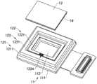
图4示出了根据本发明的上述第一实施例的所述摄像模组的模塑感光组件的立体爆炸示意图。FIG. 4 shows a schematic exploded perspective view of the molded photosensitive component of the camera module according to the first embodiment of the present invention.
图5A和5B示出了根据本发明的上述第一实施例的所述摄像模组的第一变形实施方式。5A and 5B illustrate a first variant embodiment of the camera module according to the above-described first embodiment of the present invention.
图6示出了根据本发明的上述第一实施例的所述摄像模组的第二变形实施方式。FIG. 6 shows a second variant embodiment of the camera module according to the above-mentioned first embodiment of the present invention.
图7示出了根据本发明的上述第一实施例的所述摄像模组的第三变形实施方式。FIG. 7 shows a third variant embodiment of the camera module according to the above-mentioned first embodiment of the present invention.
图8示出了根据本发明的上述第一实施例的所述摄像模组的第四变形实施方式。FIG. 8 shows a fourth variant embodiment of the camera module according to the above-mentioned first embodiment of the present invention.
图9示出了根据本发明的上述第一实施例的所述摄像模组的第五变形实施方式。FIG. 9 shows a fifth variant embodiment of the camera module according to the above-mentioned first embodiment of the present invention.
图10A是根据本发明的一第二实施例的一种摄像模组的剖视示意图。10A is a schematic cross-sectional view of a camera module according to a second embodiment of the present invention.
图10B示出了根据本发明的上述第二实施例的所述摄像模组的模塑摄像模组的立体爆炸示意图。FIG. 10B shows a schematic exploded perspective view of the molded camera module of the camera module according to the second embodiment of the present invention.
图11A和11B示出了根据本发明的上述第二实施例的所述摄像模组的一个变形实施方式。11A and 11B illustrate a modified implementation of the camera module according to the above-mentioned second embodiment of the present invention.
图12示出了根据本发明的一第三实施例的摄像模组的制造步骤之一的示意图。FIG. 12 is a schematic diagram illustrating one of the manufacturing steps of the camera module according to a third embodiment of the present invention.
图13A示出了根据本发明的上述第三实施例的所述摄像模组的制造步骤之二的示意图。FIG. 13A shows a schematic diagram of the second manufacturing step of the camera module according to the third embodiment of the present invention.
图13B示出了根据本发明的上述第三实施例的所述摄像模组的所述制造步骤之二的一个变形实施方式。FIG. 13B shows a modified embodiment of the second manufacturing step of the camera module according to the third embodiment of the present invention.
图14示出了根据本发明的上述第三实施例的所述摄像模组的制造步骤之三的示意图。FIG. 14 shows a schematic diagram of the third manufacturing step of the camera module according to the third embodiment of the present invention.
图15是根据本发明的一实施例的一种摄像模组的制造方法的流程示意图。FIG. 15 is a schematic flowchart of a method for manufacturing a camera module according to an embodiment of the present invention.
图16示出了根据本发明的所述摄像模组的制造方法中粘接滤光构件的流程示意图。FIG. 16 shows a schematic flow chart of bonding the filter member in the manufacturing method of the camera module according to the present invention.
图17示出了根据本发明的所述摄像模组的制造方法中组装光学镜头的流程示意图。FIG. 17 shows a schematic flow chart of assembling an optical lens in the manufacturing method of the camera module according to the present invention.
图18是一种配置有根据本发明的所述摄像模组的电子设备的一个示例。FIG. 18 is an example of an electronic device equipped with the camera module according to the present invention.
具体实施方式Detailed ways
以下描述用于揭露本发明以使本领域技术人员能够实现本发明。以下描述中的优选实施例只作为举例,本领域技术人员可以想到其他显而易见的变型。在以下描述中界定的本发明的基本原理可以应用于其他实施方案、变形方案、改进方案、等同方案以及没有背离本发明的精神和范围的其他技术方案。The following description serves to disclose the invention to enable those skilled in the art to practice the invention. The preferred embodiments described below are given by way of example only, and other obvious modifications will occur to those skilled in the art. The basic principles of the invention defined in the following description may be applied to other embodiments, variations, improvements, equivalents, and other technical solutions without departing from the spirit and scope of the invention.
本领域技术人员应理解的是,在本发明的揭露中,术语“纵向”、“横向”、“上”、“下”、“前”、“后”、“左”、“右”、“竖直”、“水平”、“顶”、“底”“内”、“外”等指示的方位或位置关系是基于附图所示的方位或位置关系,其仅是为了便于描述本发明和简化描述,而不是指示或暗示所指的装置或元件必须具有特定的方位、以特定的方位构造和操作,因此上述术语不能理解为对本发明的限制。It should be understood by those skilled in the art that in the disclosure of the present invention, the terms "portrait", "horizontal", "upper", "lower", "front", "rear", "left", "right", " The orientation or positional relationship indicated by vertical, horizontal, top, bottom, inner, outer, etc. is based on the orientation or positional relationship shown in the accompanying drawings, which are only for the convenience of describing the present invention and The description is simplified rather than indicating or implying that the device or element referred to must have a particular orientation, be constructed and operate in a particular orientation, and thus the above terms should not be construed as limiting the invention.
在本发明中,权利要求和说明书中术语“一”应理解为“一个或多个”,即在一个实施例,一个元件的数量可以为一个,而在另外的实施例中,该元件的数量可以为多个。除非在本发明的揭露中明确示意该元件的数量只有一个,否则术语“一”并不能理解为唯一或单一,术语“一”不能理解为对数量的限制。In the present invention, the term "a" in the claims and the description should be understood as "one or more", that is, in one embodiment, the number of an element may be one, and in another embodiment, the number of the element may be one Can be multiple. Unless it is clearly indicated in the disclosure of the present invention that the number of the element is only one, the term "a" should not be construed as unique or single, and the term "a" should not be construed as a limitation on the number.
在本发明的描述中,需要理解的是,属于“第一”、“第二”等仅用于描述目的,而不能理解为指示或者暗示相对重要性。本发明的描述中,需要说明的是,除非另有明确的规定和限定,属于“相连”、“连接”应做广义理解,例如,可以是固定连接,也可以是可拆卸连接或者一体地连接;可以是机械连接,也可以是电连接;可以是直接连接,也可以是通过媒介间接连结。对于本领域的普通技术人员而言,可以根据具体情况理解上述术语在本发明中的具体含义。In the description of the present invention, it should be understood that references to "first", "second", etc. are only for descriptive purposes, and should not be construed as indicating or implying relative importance. In the description of the present invention, it should be noted that, unless otherwise expressly specified and limited, “connected” and “connected” should be understood in a broad sense, for example, it may be a fixed connection, a detachable connection or an integral connection ; It can be a mechanical connection or an electrical connection; it can be a direct connection or an indirect connection through a medium. For those of ordinary skill in the art, the specific meanings of the above terms in the present invention can be understood according to specific situations.
在本说明书的描述中,参考术语“一个实施例”、“一些实施例”、“示例”、“具体示例”、或“一些示例”等的描述意指结合该实施例或示例描述的具体特征、结构、材料或者特点包含于本发明的至少一个实施例或示例中。在本说明书中,对上述术语的示意性表述不必须针对的是相同的实施例或示例。而且,描述的具体特征、结构、材料或者特点可以在任一个或多个实施例或示例中以合适的方式结合。此外,在不相互矛盾的情况下,本领域的技术人员可以将本说明书中描述的不同实施例或示例以及不同实施例或示例的特征进行结合和组合。In the description of this specification, description with reference to the terms "one embodiment," "some embodiments," "example," "specific example," or "some examples", etc., mean specific features described in connection with the embodiment or example , structure, material or feature is included in at least one embodiment or example of the present invention. In this specification, schematic representations of the above terms are not necessarily directed to the same embodiment or example. Furthermore, the particular features, structures, materials or characteristics described may be combined in any suitable manner in any one or more embodiments or examples. Furthermore, those skilled in the art may combine and combine the different embodiments or examples described in this specification, as well as the features of the different embodiments or examples, without conflicting each other.
随着模塑工艺的日益成熟,IOM(IR on Molding,滤光元件在模塑上)技术也逐渐被应用于摄像模组的封装过程中,以追逐小型化、轻薄化的发展潮流。特别地,如图1所示,现有的摄像模组1P为了进一步降低摄像模组的高度,通常会将所述模塑基座32P上贴附所述滤光片33P的部位向下凹陷以形成所述凹槽35P,使得所述模塑基座32P上贴附所述滤光片33P的部位低于安装所述光学镜头2P的部位,以使所述模塑基座32P形成内凹式阶梯结构,以便最大限度地缩小所述滤光片33P与所述成像组件31P的感光芯片311P之间的距离。As the molding process becomes more and more mature, the IOM (IR on Molding, filter element on molding) technology is also gradually applied to the packaging process of the camera module to pursue the development trend of miniaturization and thinning. In particular, as shown in FIG. 1 , in order to further reduce the height of the
然而,由于所述模塑基座32P的所述凹槽35P的拐角处并非直角,而会因模塑过程中覆膜工艺在所述凹槽35P的拐角处形成一过渡弧面351P,使得所述过渡弧面351P不可避免地会影响所述模塑基座32P提供平整的贴附面,因此在贴附所述滤光片33P时,所述滤光片33P不得不避让所述模塑基座32P上的所述过渡弧面351P,以确保所述滤光片33P被平整地贴附在所述模塑基座32P上。但为了避让所述凹槽35P的所述过渡弧面351P,所述滤光片22P的边缘将不得不远离所述凹槽35P的外侧壁,使得所述滤光片33P与所述模塑基座32P之间的接触面积不得不减小,即所述滤光片33P的底部支撑面积不得不变小,导致所述滤光片33P与所述模塑基座32P之间的连接强度大幅降低,进而影响摄像模组的可靠性。However, since the corners of the
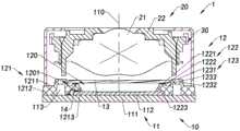
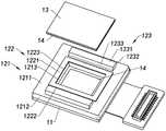
因此,为了解决上述问题,本发明提供了一种摄像模组和模塑感光组件及其制造方法,以便消除在模塑工艺中覆膜产生的过渡弧面对滤光构件产生的不利影响。具体地,如图2至图4所示,根据本发明的一第一实施例的一种摄像模组1被阐明,其中所述摄像模组1包括一模塑感光组件10和至少一光学镜头20,其中所述模塑感光组件10包括一成像组件11、一模塑基座12以及一滤光构件13,其中所述模塑基座12被模塑成型于所述成像组件11,并且所述滤光构件13被贴附于所述模塑基座12;其中所述光学镜头20被对应地设置于所述模组感光组件10,并且所述光学镜头20对应于所述成像组件11的感光路径110,以组装成所述摄像模组1。Therefore, in order to solve the above problems, the present invention provides a camera module, a molded photosensitive assembly and a manufacturing method thereof, so as to eliminate the adverse effect on the filter member caused by the transition arc generated by the coating during the molding process. Specifically, as shown in FIGS. 2 to 4 , a camera module 1 according to a first embodiment of the present invention is illustrated, wherein the camera module 1 includes a molded
值得一提的是,尽管在附图2至图4和接下来的描述中以所述摄像模组仅包括一个所述光学镜头20为例,阐述本发明的所述摄像模组的特征和优势,本领域的技术人员可以理解的是,附图2至图4以及接下来的描述中揭露的所述摄像模组仅为举例,其并不构成对本发明的内容和范围的限制,例如,在所述摄像模组的其他示例中,所述光学镜头20的数量也可以超过一个,以形成阵列摄像模组。It is worth mentioning that, although the camera module includes only one
特别地,如图3所示,所述模塑感光组件10的所述模塑基座12包括一第一模塑部121、一第二模塑部122以及一第三模塑部123。所述第一模塑部121包覆所述成像组件11的一部分。所述第二模塑部122一体地形成于所述第一模塑部121的第一上表面1211,其中所述第二模塑部122具有一第二上表面1221,并且所述第二模塑部122的第二上表面1221高于所述第一模塑部121的所述第一上表面1211,以通过所述第二模塑部122的第二外侧面1222与所述第一模塑部121的所述第一上表面1211定义形成一外空间1201,也就是说,所述模塑基座12通过所述第二模塑部122的第二上表面1221为所述滤光构件13提供一高于所述第一上表面1211的贴附面,便于将所述滤光构件13贴附于所述模塑基座12的所述第二模塑部122。所述第三模塑部123一体地形成于所述第一模塑部121的所述第一上表面1211,其中所述第三模塑部123位于所述第二模塑部122的外侧,并且所述第三模塑部123与所述第二模塑部122间隔地设置,以在所述第三模塑部123与所述第二模塑部122之间形成所述外空间1201。Particularly, as shown in FIG. 3 , the
换言之,在本发明的这个实施例中,所述第二模塑部122和所述第三模塑部123均自所述第一模塑部121的所述第一上表面1211一体地向上延伸,以形成具有一体式结构的所述模塑基座12。也就是说,所述第二模塑部122和所述第三模塑部123均能够通过模塑工艺一体成型于所述第一模塑部121的所述第一上表面1211,使得整个所述模塑基座12具有一体式结构。可以理解的是,所述第一模塑部121的内部上下贯穿,以形成所述模塑基座12的光窗120,其中所述第二模塑部122围绕所述模塑基座12的所述光窗120,并且所述模塑基座12的所述光窗120对应于所述成像组件11的所述感光路径110。In other words, in this embodiment of the present invention, both the
这样尽管在模塑过程中仍会因覆膜而在所述第三模塑部123的第三内侧面1233与所述第一模塑部121的所述第一上表面1211之间的连接处形成过渡弧面,但是由于所述第二模塑部122的所述第二上表面1221高于所述模塑基座12上的所述过渡弧面,即所述滤光构件13的贴附面高于所述模塑基座12上的所述过渡弧面,因此在将所述滤光构件13贴附至所述模塑基座12的所述贴附面时,所述滤光构件13的边缘能够处于所述外空间1201之内,而无需避让所述模塑基座12上的所述过渡弧面,使得所述滤光构件13的边缘能够尽可能地靠近所述第三模塑部123的所述第三内侧面1233,有助于增大所述滤光构件13的贴附面积,即所述滤光构件13的底部支撑面积得以变大,有助于增强所述滤光构件13与所述模塑基座12之间的连接强度,进而提高所述摄像模组1的可靠性。In this way, even in the molding process, the connection between the third
进一步地,如图3所示,由于所述模塑基座12的所述第二模塑部122的所述第二上表面1221高于所述第一模塑部121的所述第一上表面1211,并且所述第二模塑部122的所述第二上表面1221与所述模塑基座12上的所述过渡弧面之间没有接壤,因此所述模塑基座12能够通过所述第二模塑部122的所述第二上表面1221为所述滤光构件13提供一平整的贴附面。Further, as shown in FIG. 3 , because the second
优选地,所述第二模塑部122的所述第二上表面1221为一平整面,以便将所述滤光构件13平整地贴附于所述模塑基座12,保证所述滤光构件13具有良好的贴附质量。值得注意的是,受限于模塑工艺的模具压头尺寸,以及所述摄像模组1自身高度的考量,所述第二模塑部122的所述第二上表面1221相对于所述第一模塑部121的所述第一上表面1211的高度范围优选地被实施为0.03毫米至0.2毫米,即所述第二模塑部122的所述第二上表面1221与所述第一模塑部121的所述第一上表面1211之间的高度差h在0.03毫米至0.2毫米之间(如图3所示)。这样既能够满足模塑工艺的模具压头尺寸的需要,又能够避免因所述第二模塑部122的所述第二上表面1221过高而导致所述滤光构件13的安装高度较大,进而造成所述摄像模组1的自身高度变大。Preferably, the second
此外,如图3和图4所示,所述模塑基座12的所述第三模塑部123位于所述第二模塑部122的外侧,并且所述第三模塑部123与所述第二模塑部122间隔设置,以在所述第三模塑部123和所述第二模塑部122之间预留出所述模塑基座12的所述外空间1201。换言之,所述第三模塑部123的第三内侧面1233位于所述第二模塑部122的所述第二外侧面1222的外侧,也就是说,所述第三模塑部123的所述第三内侧面1233与所述成像组件11的所述感光路径110之间的最小距离r3大于所述第二模塑部122的所述第二外侧面1222与所述成像组件11的所述感光路径110之间的最大距离R2,即r3>R2,以通过所述第一模塑部121的所述第一上表面1211与所述第二模塑部122的所述第二上表面1221和所述第三模塑部123的所述第三上表面1231之间高度差,在所述模塑基座12上形成凹槽,即在所述第三模塑部123的所述第三内侧面1233与所述第二模塑部122的所述第二外侧面1222之间形成所述模塑基座12的所述外空间1201,以便在贴附所述滤光构件13时,所述滤光构件13的边缘能够伸入所述外空间1201以靠近所述第三模塑部123的所述第三内侧面1233,而不会受到所述第三模塑部123的所述第三内侧面1233与所述第一模塑部121的所述第一上表面1211之间的过渡弧面的影响。In addition, as shown in FIGS. 3 and 4 , the
优选地,受限于模塑工艺的最小模具压头尺寸,所述第三模塑部123的第三内侧面1233与所述第二模塑部122的所述第二外侧面1222之间的距离d不小于0.01毫米(如图3所示),也就是说,所述模塑基座12的所述外空间1201的宽度不小于0.01毫米。Preferably, limited by the minimum die indenter size of the molding process, the distance between the third
当然,在本发明的这个实施例中,由于所述第一模塑部121的内部上下贯穿,即所述第一模塑部121的第一内侧面1213定义出所述模塑基座12的所述光窗120。因此,如图3所示,所述第二模塑部122的第二内侧面1223与所述成像组件11的所述感光路径110之间的最小距离r2不小于所述第一模塑部121的所述第一内侧面1213与所述成像组件11的所述感光路径110之间的最大距离r1,即r2≥r1,以防所述第二模塑部122遮挡所述成像组件11的所述感光路径110。Of course, in this embodiment of the present invention, since the interior of the
值得一提的是,在本发明的所述第一实施例中,如图3和图4所示,所述成像组件11包括一线路板111和至少一感光元件112,其中每个所述感光元件112分别被可导通地贴装于所述线路板111的不同位置,并且每个所述感光元件112的感光区域对应于相应的所述光学镜头20。此外,当所述滤光构件13被对应地贴附于所述模塑基座12的所述第二模塑部122时,所述滤光构件13对应于所述感光元件112,并在所述滤光构件13和所述感光元件112之间形成所述模塑感光组件10的一内部空间100。It is worth mentioning that, in the first embodiment of the present invention, as shown in FIG. 3 and FIG. 4 , the
进一步地,如图3和图4所示,所述模塑感光组件10还可以包括一粘接层14,其中所述粘接层14由粘接剂固化之后形成,并且所述粘接层14位于所述滤光构件13的下表面131和所述第二模塑部122的所述第二上表面1221之间,以将所述滤光构件13牢靠地贴附于所述模塑部基座12,使得所述滤光构件13对应于所述成像组件11的所述感光路径110。更具体地,当所述滤光构件13被贴附于所述模塑基座12的所述第二模塑部122时,所述滤光构件13的所述下表面131朝下以面向所述成像组件11,并且所述滤光构件13的上表面132相应地朝上以面向所述光学镜头20。Further, as shown in FIG. 3 and FIG. 4 , the molded
而由于形成所述粘接层14的粘接剂在固化之前具有一定的流动性,特别是在贴附所述滤光构件13时,所述滤光构件13将对固化前的粘接剂施压,导致固化前的粘接剂必然会发生溢流,因此所述外空间1201的存在还可以引导所述粘接剂向外溢流,便于在一定程度上减少所述粘接剂向内溢流,以免所述粘接剂向内流至所述第一模塑部121的所述第一内侧面1213和所述成像组件11的所述感光元件112,有助于降低所述粘接剂影响所述摄像模组1的成像质量的风险。Since the adhesive forming the
换言之,正是由于所述模塑基座12的所述第二模塑部122的所述第二上表面1221高于所述第一模塑部121的所述第一上表面1211,使得所述模塑基座12的所述外空间1201位于所述第二模塑部122的周围,并作为所述模塑基座12上用于容纳粘接剂的外溢空间,因此当所述滤光构件13通过粘接剂被贴附于所述第二模塑部122的所述第二上表面1221时,所述第二模塑部122的外周缘能够位于所述模塑基座12的所述外空间1201,使得固化前的粘接剂能够向外溢流至所述模塑基座12的所述外空间1201(即所述模塑基座12的所述外空间1201可以作为所述模塑基座12的外溢胶空间),以减小所述粘接剂向内溢流的量,有助于降低因所述粘接剂向内溢流至所述感光元件112而影响所述摄像模组1的成像质量的风险。In other words, it is precisely because the second
可以理解的是,对于现有的摄像模组1P而言,如图1所示,虽然在所述模塑基座32P上设置凹槽35P能够进一步减小所述滤光片33P与所述感光芯片311P之间的距离,以最大限度地缩小所述感光组件30P的厚度,但是在所述滤光片33P被贴附于所述模塑基座32P的所述凹槽35P之后,所述滤光片33P的周围不仅没有溢胶空间,而且所述模塑基座32P的所述凹槽35P的所述过渡弧面351P还会不可避免地阻挡用于粘接所述滤光片33P的胶水向外溢胶,导致更多的胶水将会向内溢胶,极易造成胶水向内溢流至所述成像组件31P的所述感光芯片311P,对所述感光芯片311P造成污染,进而影响摄像模组的成像质量。而在本发明的上述第一实施例的所述摄像模组1中,所述模塑感光组件10的所述模塑基座12不仅能够提供足够大且平整的贴附面,用于在无需避让过渡弧面的情况下牢靠地且平整地贴附所述滤光构件13;而且还能够提供粘接剂向外溢流的外溢空间,以缓解固化前的粘接剂向内溢流而影响摄像模组的成像质量。It can be understood that, for the existing
值得注意的是,在本发明的上述第一实施例中,所述模塑感光组件10的所述粘接层14可以但不限于由诸如热固化胶等等之类的胶水固化而成,换言之,形成所述粘接层14的所述粘接剂可以但不限于被实施为诸如热固化胶等等之类的胶水。当然,在本发明的其他示例中,形成所述粘接层14的所述粘接剂还可以被实施为诸如光固化胶其他类型的粘性材料,只要能够形成所述粘接层14以将所述滤光构件13牢靠地贴附于所述第二模塑部122的所述第二上表面1221即可,本发明对此不再赘述。It is worth noting that in the above-mentioned first embodiment of the present invention, the
根据本发明的上述第一实施例,如图3所示,本发明的所述模塑感光组件10的所述成像组件11通常还会包括一组电子元器件113,其中每个所述电子元器件113可以通过诸如SMT(Surface Mount Technology,表面安装技术)工艺被相互间隔地安装于所述线路板111的边缘区域,并且每所述电子元器件113分别与所述线路板111可导通地连接。可以理解的是每个所述电子元器件113可以分别位于所述感光元件112的四周,也可以位于所述感光元件112的同一侧或相对两侧,例如在一个具体示例中,所有的所述电子元器件113可以分为两列,并且被对称地设置于所述感光元件112的两侧。According to the above-mentioned first embodiment of the present invention, as shown in FIG. 3 , the
然而,由于模塑工艺存在最小厚度,模塑厚度太小会导致模塑成像困难,因此为了确保所述模塑基座12能够完整地包覆所述电子元器件113,所述模塑基座12的所述第三模塑部123优选地对应于所述成像组件11的所述电子元器件113,并且所述第三模塑部123的所述第三上表面1231高于所述电子元器件113的顶表面,对应于所述成像组件11的所述电子元器件113,以通过所述第三模塑部123来保证所述电子元器件113上方具有足够的模塑成型厚度。However, due to the minimum thickness in the molding process, too small molding thickness will lead to difficulty in molding and imaging. Therefore, in order to ensure that the
换句话说,如图3和图4所示,所述第三模塑部123被一体地成型于所述第一模塑部121的所述第一上表面1211,以使所述第三模塑部123的所述第三上表面1231高于所述第一模塑部121的所述第一上表面1211。此外,由于所述第三模塑部123对应于所述成像组件11的所述电子元器件113,因此所述第一模塑部121的所述第一上表面1211可以不必高于所述电子元器件113的顶表面,以通过所述第三模塑部123和所述第一模塑部121来完整地包覆所述电子元器件113。可以理解的是,所述模塑基座12在成型后包覆每个所述电子元器件113,以藉由所述模塑基座12隔离相邻所述电子元器件113和隔离所述电子元器件113与所述感光元件112,使得相邻所述电子元器件113之间不会出现相互干扰的不良现象,即便是相邻所述电子元器件113的距离较近时也能够保证所述摄像模组1的成像品质。这样可以在小面积的所述线路板111上贴装更多数量的所述电子元器件113,从而使所述模塑感光组件10的结构更加的紧凑,以有利于在控制所述摄像模组1的尺寸的基础上提高所述摄像模组1的成像品质。In other words, as shown in FIGS. 3 and 4 , the
值得注意的是,正是由于所述第一模塑部121的所述第一上表面1211可以低于所述电子元器件113的顶表面,使得所述第二模塑部122的所述第二上表面1221可以不受所述电子元器件113的尺寸影响,即所述第二模塑部122的所述第二上表面1221也可以低于所述电子元器件113的顶表面,因此所述第二模塑部122的所述第二上表面1221也可以降低,使得所述滤光构件13的贴附高度得以降低,有助于缩短所述滤光构件13与所述成像组件11的所述感光元件112之间的距离,以便缩小所述摄像模组1的后焦,有利于缩减所述摄像模组1的高度。It is worth noting that because the first
值得一提的是,在本发明的这个第一实施例中,所述滤光构件13包括至少一滤光元件,其中每个所述滤光元件分别对应地设置于所述成像组件11的所述感光元件112,以在每个所述滤光元件和所述感光元件112之间分别形成每个所述内部空间100。此外,所述滤光元件位于所述光学镜头20和所述感光元件112之间,以使自所述光学镜头20进入所述摄像模组1的内部的光线在穿过所述滤光元件的过滤后,才能够被所述感光元件112的所述感光区域接收和进行光电转化,从而改善所述摄像模组的成像品质,例如所述滤光元件可以过滤自所述光学镜头20进入所述摄像模组1的内部的光线中的红外线部分。当然,在本发明的其他示例中,所述滤光构件13还可以包括一贴附框架(图中未示出),其中所述贴附框架位于所述滤光元件的边缘,以通过所述贴附框架避免所述滤光元件与所述粘接层14直接接触,以避免所述滤光元件被所述粘接层14污染或腐蚀,有效地延长所述滤光元件的使用寿命。可以理解的是,在所述摄像模组1的不同示例中,所述滤光元件能够被实施为不同的类型,例如所述滤光元件能够被实施为红外截止滤光片、全透光谱滤光片以及其他的滤光片或者多个滤光片的组合。It is worth mentioning that, in the first embodiment of the present invention, the
此外,根据本发明的上述第一实施例,参考附图2和图3,所述摄像模组1还可以包括至少一驱动器30,其中每个所述光学镜头20分别被组装于每个所述驱动器30,每个所述驱动器30分别被组装于所述模塑基座12的所述第三模塑部123的所述第三上表面1231,以使每个所述光学镜头10分别被保持在所述模塑感光组件10的所述成像组件11的所述感光路径110,以组装成变焦摄像模组。另外,在使用所述摄像模组1时,所述驱动器30能够驱动所述光学镜头20沿着所述成像组件11的所述感光路径110来回移动,以通过调整所述光学镜头20和所述感光元件112的距离的方式调整所述摄像模组1的焦距。本发明的所述摄像模组的所述驱动器30的类型不受限制,所述驱动器30可以被实施为音圈马达,其能够被电连接于所述线路板111,以在接收电能和控制信号后处于工作状态,而驱动所述光学镜头20沿着所述成像组件11的所述感光路径110来回移动。尽管如此,本领域的技术人员可以理解的是,所述驱动器30的类型不受限制,其只要能够驱动所述光学镜头20沿着所述成像组件11的所述感光路径110来回移动即可。In addition, according to the above-mentioned first embodiment of the present invention, referring to FIGS. 2 and 3 , the camera module 1 may further include at least one
具体地说,如图2和图3所示,所述摄像模组1的所述光学镜头20包括一镜筒21和一镜片组22,其中所述镜筒21被组装于所述驱动器30,并且所述镜片组22被组装于所述镜筒21,其中所述驱动器30被安装于所述模塑基座12的所述第三模塑部123的所述第三上表面1231,以藉由所述驱动器30使所述光学镜头20的所述镜片组22被保持在所述模塑感光组件10的所述成像组件11的所述感光路径110。Specifically, as shown in FIGS. 2 and 3 , the
可以理解的是,在本发明的其他示例中,所述摄像模组1也可以不包括任何驱动器30,换言之,所述光学镜头20的所述镜筒21直接被组装于所述模塑基座12的所述第三模塑部123的所述第三上表面1231,其中所述镜片组22被组装于所述镜筒21,以藉由所述镜筒21使所述光学镜头20的所述镜片组22被保持在所述模塑感光组件10的所述成像组件11的所述感光路径110。当然,在本发明的另一示例中,所述光学镜头20的所述镜筒21也可以与所述模塑基座12的所述第三模塑部123通过模塑工艺藉由成型材料一体地固化成型,从而增强所述摄像模组1的稳定性和可靠性,本发明对此不再赘述。It can be understood that, in other examples of the present invention, the camera module 1 may not include any
附图5A和5B示出了根据本发明上述第一实施例的所述摄像模组1的第一变形实施方式。具体地,相比于根据本发明的上述第一实施例,根据本发明的所述第一变形实施方式的所述摄像模组1的区别在于:所述模塑基座12的所述第三模塑部123的第三外侧面1232位于所述第一模塑部121的所述第一外侧面1221的内侧,也就是说,所述第三模塑部123的所述第三外侧面1232与所述成像组件11的所述感光路径110之间的最大距离R3小于所述第一模塑部121的所述第一外侧面1221与所述成像组件11的所述感光路径110之间的最小距离R1,即R3<R1,以在所述第一模塑部121的所述第一上表面1211上且所述第三模塑部123的外侧为所述驱动器30预留安装空间,以便将所述驱动器30对应地安装至所述第一模塑部121的所述第一上表面1211,有助于降低所述摄像模组1的整体高度。5A and 5B show a first variant embodiment of the camera module 1 according to the above-mentioned first embodiment of the present invention. Specifically, compared with the above-mentioned first embodiment of the present invention, the camera module 1 according to the first modified embodiment of the present invention is different in that the third The third
换句话说,如图5A所示,所述模塑基座12的所述第三模塑部123的第三外侧面1232位于所述第一模塑部121的所述第一外侧面1221的内侧,使得所述驱动器30能够直接被安装至所述模塑基座12的所述第一模塑部121的所述第一上表面1211。而由于所述第一模塑部121的所述第一上表面1211低于所述第三模塑部123的所述第三上表面1231,使得所述驱动器30的安装高度得以降低,有助于降低所述摄像模组1的整体高度。In other words, as shown in FIG. 5A , the third
值得一提的是,在本发明的这个变形实施方式中,由于所述第三模塑部123只需包覆所述电子元器件113的顶部即可,即所述第三模塑部123的位置仅对应于所述成像组件11的所述电子元器件113即可,因此所述第三模塑部123不需要具有环形结构,而可以根据所述电子元器件113的位置和尺寸来设计所述第三模塑部123的位置和尺寸。例如,如图5B所示,当所有的所述电子元器件113仅位于所述滤光构件13的长边之外时,所述第三模塑部123可以被实施为位于所述滤光构件13的长边之外的两个条状凸起,以通过所述条状凸起来包覆所有的所述电子元器件113,而所述滤光元件13的短边之外则不设置所述第三模塑部123,以降低所述模塑基座12的重量。It is worth mentioning that, in this modified embodiment of the present invention, since the
优选地,如图5A所示,所述第三模塑部123的高度大于所述第二模塑部122,也就是说,所述第三模塑部123的所述第三上表面1231高于所述第二模塑部122的所述第二上表面1221,使得所述第三模塑部123更容易成型。特别地,相比于如图1所示的现有的摄像模组,尽管所述第三模塑部123的所述第三内侧面1233与所述第一模塑部121的所述第一上表面1211的连接处仍存在过渡弧面,但由于所述第二模塑部122的所述第二上表面1221高于所述第一模塑部121的所述第一上表面1211(即所述第二模塑部122的所述第二上表面1221位于所述过渡弧面之上)。这样在将所述滤光构件13贴附于所述第二模塑部122的所述第二上表面1221时,所述滤光构件13的边缘无需避让所述过渡弧面,使得所述滤光构件13的边缘能够更靠近所述第三模塑部123,以最大限度地增大所述滤光构件13的底部支撑面积,有助于提高所述摄像模组1的可靠性。Preferably, as shown in FIG. 5A , the height of the
更优选地,如图5A所示,所述第三模塑部123的所述第三上表面1231高于所述滤光构件13的上表面132,并且所述第三模塑部123的所述第三上表面1231对应于所述光学镜头20,以使所述第三模塑部123的所述第三上表面1231与所述光学镜头20之间的最小距离小于所述滤光构件13的所述上表面132与所述光学镜头20之间的最小距离。这样在所述摄像模组1的调焦或对焦的过程中,当所述光学镜头20被所述驱动器30驱动以靠近所述成像组件11的所述感光元件112时,所述第三模塑部123还能够阻挡所述光学镜头20接触所述滤光构件13,以防所述光学镜头20与所述滤光构件13发生碰撞,从而有效地保护所述滤光构件13和所述光学镜头20不受损坏。More preferably, as shown in FIG. 5A , the third
最优选地,如图5A所示,所述第三模塑部123的所述第三上表面1231仅对应于所述光学镜头20的所述镜筒22,以在所述光学镜头20被所述驱动器30驱动以靠近所述成像组件11的所述感光元件112时,所述第三模塑部123仅能够与所述光学镜头20的所述镜筒22接触以阻挡所述光学镜头20接触所述滤光构件13,进而避免所述第三模塑部123与所述光学镜头20的所述镜片组21发生碰撞,有助于保护所述光学镜头20的所述镜片组21。Most preferably, as shown in FIG. 5A , the third
附图6示出了根据本发明的上述第一实施例的所述摄像模组1的第二个变形实施方式。具体地,相比于根据本发明的上述第一变形实施方式,根据本发明的所述第二变形实施方式的所述摄像模组1的区别在于:所述模塑感光组件10的所述模塑基座12还可以包括一第四模塑部124,其中所述第四模塑部124自所述第一模塑部121的所述第一上表面1211向下凹陷,并且所述第四模塑部124位于所述第三模塑部123的外侧,以在所述第一模塑部121的外周缘形成一周缘槽,使得所述周缘槽的底面作为所述第四模塑部124的第四上表面1241,以通过所述第四模塑部124的所述第四上表面1241提供所述驱动器30(或所述光学镜头20)的安装面,使得所述驱动器30(或所述光学镜头20)能够被安装于所述第四模塑部124的所述第四上表面1241。FIG. 6 shows a second variant embodiment of the camera module 1 according to the above-mentioned first embodiment of the present invention. Specifically, compared with the above-mentioned first modified embodiment of the present invention, the camera module 1 according to the second modified embodiment of the present invention is different in that: the mold for molding the
换言之,所述第四模塑部124的所述第四上表面1241低于所述第一模塑部121的所述第一上表面1211,有助于进一步降低了所述驱动器30的安装高度,从而进一步降低所述摄像模组1的整体高度。特别地,在本发明的这个第二变形实施方式中,所述第四模塑部124位于所述第一模塑部121的外周缘,使得所述第四模塑部124的所述第四上表面1241可以大幅地低于所述电子元器件113的顶表面,有助于最大限度地降低了所述驱动器30的安装高度,使得所述摄像模组1的高度得以最小。In other words, the fourth
优选地,如图6所示,所述第四模塑部124的所述第四上表面1241与所述驱动器30的端面相匹配,以在所述驱动器30被安装至所述第四模塑部124的所述第四上表面1241时,所述驱动器30的外周表面与所述模塑基座12的所述第一模塑部121的所述第一外侧面1221齐平,有助于最大限度地减小所述摄像模组1的尺寸,同时也有利于美化所述摄像模组1的外观。Preferably, as shown in FIG. 6 , the fourth
附图7示出了根据本发明的上述第一实施例的所述摄像模组1的第三个变形实施方式。具体地,相比于根据本发明的上述第一变形实施方式,根据本发明的所述第三变形实施方式的所述摄像模组1的区别在于:所述模塑感光组件10的所述模塑基座12还可以包括一第四模塑部124’,其中所述第四模塑部124自所述第一模塑部121的所述第一上表面1211向上延伸,并且所述第四模塑部124’位于所述第三模塑部123的外侧,以在所述第一模塑部121的外周缘形成一周缘凸起,以通过所述第四模塑部124’的第四上表面1241’提供所述驱动器30(或所述光学镜头20)的安装面,以便满足所述驱动器30的安装需要。换言之,受限于所述驱动器30和所述光学镜头20的安装要求,所述第四模塑部124’的所述第四上表面1241’的高度需要根据所述驱动器30的安装需求进行设计,,以便将所述驱动器30适配地安装于所述第四模塑部124’的所述第四上表面1241’。例如,所述第四模塑部124’的所述第四上表面1241’可以高于所述第一模塑部121的所述第一上表面1211,并且低于所述第三模塑部123的所述第三上表面1231。当然,在本发明的其他示例中,所述第四模塑部124’的所述第四上表面1241’也可以高于所述第三模塑部123的所述第三上表面1231,以满足所述驱动器30的安装需求。FIG. 7 shows a third variant embodiment of the camera module 1 according to the above-mentioned first embodiment of the present invention. Specifically, compared with the above-mentioned first modified embodiment of the present invention, the camera module 1 according to the third modified embodiment of the present invention is different in that: the mold for molding the
附图8示出了根据本发明的上述第一实施例的所述摄像模组1的第四个变形实施方式。具体地,相比于根据本发明的上述第一实施例,根据本发明的所述第四变形实施方式的所述摄像模组1的区别在于:所述模塑感光组件10的所述模塑基座12不包括所述第三模塑部123,其中所述模塑基座12的所述第一模塑部121的所述第一上表面1211高于所述成像组件11的所述电子元器件113的顶表面,以通过所述第一模塑部121完整地包覆所述电子元器件113,其中所述驱动器30直接被安装至所述第一模塑部121的所述第一上表面1211。FIG. 8 shows a fourth variant embodiment of the camera module 1 according to the above-mentioned first embodiment of the present invention. Specifically, compared with the above-mentioned first embodiment of the present invention, the camera module 1 according to the fourth modified embodiment of the present invention is different in that: the molding of the molded
此外,如图8所示,所述第二模塑部122的所述第二外侧面1222位于所述第一模塑部121的所述第一外侧面1221之内,也就是说,所述第二模塑部122的所述第二外侧面1222与所述成像组件11的所述感光路径110之间的最大距离R2小于所述第一模塑部121的所述第一外侧面1221与所述成像组件11的所述感光路径110之间的最小距离R1,即R2<R1,以通过所述第一模塑部121和所述第二模塑部122在所述模塑基座12上形成外阶梯结构。这样所述模塑基座12的外阶梯结构处将形成所述模塑基座12的所述外空间1201,即所述第二模塑部122的所述外侧面1222与所述第一模塑部121的所述第一上表面1211将定义形成所述模塑基座12的所述外空间1201,使得在贴附所述滤光构件13至所述第二模塑部122的所述第二上表面1221时,固化前的粘接剂能够向外溢流至所述模塑基座12的所述外空间1201(作为所述模塑基座12的外溢胶空间),以降低因粘接剂向内溢流至所述感光元件112而对所述摄像模组1成像质量产生影响的风险。In addition, as shown in FIG. 8 , the second
附图9示出了根据本发明的上述第一实施例的所述摄像模组1的第五个变形实施方式。具体地,相比于根据本发明的上述第四变形实施方式,根据本发明的所述第五变形实施方式的所述摄像模组1的区别在于:所述模塑感光组件10的所述模塑基座12的所述第二模塑部122的所述第二内侧面1223位于所述第一模塑部121的所述第一内侧面1213之外,也就是说,所述第二模塑部122的所述第二内侧面1223与所述成像组件11的所述感光路径110之间的最小距离r2大于所述第一模塑部121的所述第一内侧面1213与所述成像组件11的所述感光路径110之间的最大距离r1,即r2>r1,以通过所述第二模塑部122的所述第二内侧面1223与所述第一模塑部121的所述第一上表面1211形成所述模塑基座12的内空间1202,其中所述内空间1202位于所述第二模塑部122的内侧(以作为所述模塑基座12的内溢胶空间),用于储放自所述第二模塑部122的所述第二上表面1221向内溢流的粘接剂,以防粘接剂向内溢流至所述感光元件112的感光区域,有助于保证所述摄像模组1的成像质量。FIG. 9 shows a fifth variant embodiment of the camera module 1 according to the above-mentioned first embodiment of the present invention. Specifically, compared with the above-mentioned fourth variant embodiment of the present invention, the camera module 1 according to the fifth variant embodiment of the present invention is different in that: the mold for molding the
值得一提的是,由于所述滤光构件13通过所述粘接层14被粘接地贴附于所述第二模塑部122的所述第二上表面1221之后,所述滤光构件13将密封所述模塑基座12的所述光窗120,因此在所述滤光构件13和所述成像组件11的所述感光元件112之间的所述内部空间100将形成一封闭空间。而当形成所述粘接层14的所述粘接剂为热固化胶时,在所述滤光构件13和所述模塑基座12的所述第二模塑部122的所述第二上表面1221之间施涂一圈所述热固化胶之后,需要对所述热固化胶加热或者烘烤,才能够使得所述热固化胶完全固化而形成具有环形结构的所述粘接层14。这样在对所述热固化胶加热时,位于所述滤光构件13和所述成像组件11之间的所述封闭空间内的气体将会受热膨胀,给所述滤光构件13施加向外的作用力,可能会造成所述滤光构件13的偏移或起翘,严重时还会造成所述滤光构件13的破裂。与此同时,所述封闭空间内的气体膨胀还将对所述感光元件112施加压力,也有可能造成所述感光元件112的损坏,对所述摄像模组1的组装造成难度,并且极大地降低了所述摄像模组1的可靠性。It is worth mentioning that, after the
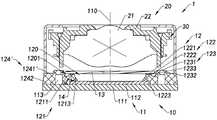
因此为了解决上述问题,本发明的一第二实施例提供了一种摄像模组和模塑感光组件。具体地,如图10A和图10B所示,相比于根据本发明的上述第一实施例,本发明的所述第二实施例的所述摄像模组1的区别在于:所述模塑感光组件10的所述模塑基座12的所述第二模塑部122设有至少一缺口1224,以当所述滤光元件13被贴附于所述第二模塑部122的所述第二上表面1221时,在所述第二模塑部122的所述缺口1224处形成所述模组基座12的一逃气孔1203,以通过所述逃气孔1203将所述模塑感光组件10的所述内部空间100与所述模塑感光组件10的外部连通,使得所述模塑感光组件10的所述内部空间100形成一非封闭空间。Therefore, in order to solve the above problems, a second embodiment of the present invention provides a camera module and a molded photosensitive component. Specifically, as shown in FIG. 10A and FIG. 10B , compared with the above-mentioned first embodiment of the present invention, the difference between the camera module 1 of the second embodiment of the present invention is that the molded photosensitive The
这样当所述粘接剂被加热以固化时,所述模塑感光组件10的所述内部空间100内的气体能够经由所述逃气孔1203逃出,以使所述模塑感光组件10的所述内部空间100内的气压保持恒定(等于大气压),避免对所述滤光元件13和所述感光元件112施加作用力,有助于保护所述滤光元件13和所述感光元件112不会因气体膨胀而被损坏。当然,在所述粘接剂被加热固化之后,所述模塑感光组件10的所述内部空间100内的气体将因冷却而缩小体积,此时所述模塑感光组件10外部的气体能够经由所述逃气孔1203进入所述模塑感光组件10的所述内部空间100,以保持所述内部空间100内的气压恒定,避免所述滤光元件13和所述感光元件112因加热或冷却而被损坏。In this way, when the adhesive is heated to be cured, the gas in the
可以理解的是,在如图1所示的现有的摄像模组1P中,由于所述滤光片33P直接被贴附于所述模塑基座32P的所述凹槽35P内,因此所述模塑基座32P上极难设置缺口以形成逃气孔,导致所述模塑感光组件3P的内部空间难以形成非封闭空间。而在本发明的所述摄像模组1中,正是由于所述第二模塑部122自所述第一模塑部121向上延伸以在所述第一模塑部121的所述第一上表面1211上形成凸起,使得所述第二模塑部122易于设置缺口,因此所述第二模塑部122不仅能够为所述滤光构件13提供平整的贴附面,而且还能够为所述模塑基座12上形成所述逃气孔1203提供便利条件。It can be understood that, in the existing
进一步地,如图10A和图10B所示,所述第二模塑部122的所述缺口1224自所述第二模塑部122的所述第二内侧面1223横向地延伸至所述第二模塑部122的所述第二外侧面1222,以在所述第二模塑部122形成横向缺口。这样当所述滤光构件13通过所述粘接层14被粘接于所述第二模塑部122的所述第二上表面1221时,所述第二模塑部122的所述缺口1224将形成横向布置的逃气孔1203,以增大灰尘经由所述逃气孔1203进入所述模塑感光组件10的所述内部空间100的难度,有助于保障所述摄像模组1的工作性能。Further, as shown in FIGS. 10A and 10B , the
优选地,如图10A所示,所述第二模塑部122的所述缺口1224对应于所述滤光构件13的长边,这样所述缺口1224的两侧具有较长的所述粘接层14来粘接所述滤光构件13,以增强所述滤光构件13与所述第二模塑部122之间的粘接强度。当然,在本发明的其他示例中,所述第二模塑部122的所述缺口1224也可以位于所述对应于所述滤光构件13的其他部位,只要能够形成将所述模塑感光组件10的所述内部空间100与所述模塑感光组件10的外部连通的所述逃气孔1203即可,本发明对此不再赘述。Preferably, as shown in FIG. 10A , the
更优选地,如图10A所示,在所述粘接剂固化以形成所述粘接层14之后,还可以在所述第二模塑部122的所述缺口1224处再次施涂粘接剂,以在粘接剂固化后形成一加强粘接块15,以通过所述加强粘接块15增强所述滤光构件13与所述第二模塑部122在所述缺口1224处的粘接强度,以确保所述滤光构件13被牢固地贴附于所述第二模塑部122。换句话说,还可以在所述模塑基座12的所述逃气孔1203处施涂粘接剂,以形成用于增强所述滤光构件13与所述第二模塑部122之间的粘接强度的所述加强粘接块15。此外,所述加强粘接块15也可以封堵所述逃气孔1203,以避免外部灰尘经由所述逃气孔1203进入所述模塑感光组件10的所述内部空间100,有助于确保所述摄像模组1的成像质量。可以理解的是,虽然所述加强粘接块15将会封堵所述逃气孔1203,但所述滤光构件13已被所述粘接层14牢靠地贴附于所述模塑基座12,并且在后续的组装和使用过程中温度变化较小,使得所述模塑感光组件10的所述内部空间100内的气压变化也较小,因此温度的变化不足以对所述滤光构件13造成实质性影响。More preferably, as shown in FIG. 10A , after the adhesive is cured to form the
附图11A和图11B示出了根据本发明的上述第二实施例的所述摄像模组1的一个变形实施方式,其中所述模塑感光组件10的所述模塑基座12还可以包括一模塑加强部125,其中所述模塑加强部125在所述第二模塑部122的所述缺口1224处自所述第二模塑部122的所述第二外侧面1222一体地向外延伸,使得所述粘接层14在所述缺口1224处的粘接面积变大,有助于增大所述滤光构件13与所述第二模塑部122在所述缺口1224处的粘接强度,以防所述滤光构件13在所述第二模塑部122的所述缺口1224处因所述粘接层14的粘接强度不足而发生开裂。11A and FIG. 11B show a modified implementation of the camera module 1 according to the above-mentioned second embodiment of the present invention, wherein the
优选地,如图11A所示,所述模塑加强部125与所述第一模塑部121一体地连接,以在所述第二模塑部122的所述第二外侧面1222与所述第一模塑部121的所述第一上表面1211之间形成加强肋,有助于增强所述第二模塑部122与所述第一模塑部121在所述缺口1224处的连接强度。Preferably, as shown in FIG. 11A , the
值得一提的是,在本发明的其他示例中,所述模塑加强部125可以自所述第二模塑部122一体地延伸至所述第三模塑部123,使得所述模塑加强部125的一端与所述第二模塑部122一体地连接,并且所述模塑加强部125的另一端与所述第三模塑部123一体地连接,有助于进一步增强所述第二模塑部122在所述缺口1224处的连接强度。It is worth mentioning that, in other examples of the present invention, the
此外,在本发明的这个变形实施方式中,所述模塑加强部123将延长所述第二模塑部122的所述缺口1224的长度,使得所述模塑基座12的所述逃气孔1203的长度也随之变长,有助于进一步增大外部灰尘经由所述逃气孔1203进入所述模塑感光组件10的所述内部空间100的难度。可以理解的是,如图11B所示,由于所述模塑加强部123凸出于所述第二模塑部122的所述第二外侧面1222,有助于引导工人或机器在所述模塑加强部123处施涂粘接剂(如补胶),以形成所述加强粘接块15。另外,所述模塑加强部123还能够防止固化前的粘接剂随意流动,以便完整地封堵所述逃气孔1203,最大限度地增强所述滤光构件13与所述第二模塑部122在所述缺口1224处的粘接强度。值得注意的是,在本发明的所述第二实施例中,除了上述结构不同之外,所述摄像模组1的其他结构与根据本发明的所述第一实施例的所述摄像模组1的结构相同,并且所述摄像模组1也具有与所述第一实施例的所述摄像模组1的各种变形实施方式相似或相同的变形实施方式,在此不再赘述。In addition, in this variant embodiment of the present invention, the
值得一提的是,参考附图12至图14所示,是本发明的一第三实施例的模组感光组件10的制造过程和摄像模组1的制造过程的示意图,本领域的技术人员应当理解,在附图12至图14中示出的所述模塑感光组件10的制造过程和所述摄像模组1的制造过程仅为示例来阐述本发明的特征和优势,其并不构成对本发明的内容和范围的限制。It is worth mentioning that, referring to FIG. 12 to FIG. 14 , it is a schematic diagram of the manufacturing process of the
具体地说,在附图12中,首先将所述感光元件112可导通地贴装于所述线路板111,以组装成所述成像组件11;之后再藉由成型模具,在所述成像组件11上模塑形成所述模塑基座12的所述第一模塑部121、具有所述缺口1224的所述第二模塑部122以及位于所述第二模塑部122外侧的第三模塑部123,其中所述第一模塑部121的所述第一上表面1211在高度方向上低于所述第二模塑部122的所述第二上表面1211,并且所述第三模塑部123与所述第二模塑部122间隔设置,以在所述第三模塑部123与所述第二模塑部122之间形成一外空间1201。可以理解的是,本发明可以通过对所述成形模具的上模具(如所述上模具中突出部的位置分布和尺寸大小等等)进行设计,以在模塑形成所述模塑基座12时,在所述第二模塑部122与所述第三模塑部123之间形成间隙或凹槽(即所述外空间1201),使得所述滤光构件13的边缘能够被容纳于所述外空间1201处,而无需避让所述模塑基座12上的过渡弧面,能够有效地消除模塑基座12上的过渡弧面对贴附滤光构件13产生的不利影响。Specifically, in FIG. 12, firstly, the
在附图13A中,先在所述模塑基座12的所述第二模塑部122的所述第二上表面1211上施涂粘接剂,以在将所述滤光构件13对应地设置于所述模塑基座12的所述光窗120之后,由所述粘接剂固化以形成位于所述滤光构件13的所述下表面131和所述第二模塑部122的所述第二上表面1211之间的粘接层14,以通过所述粘接层14将所述滤光构件13牢固地粘接于所述模塑基座12的所述第二模塑部122,以组装成所述模塑感光组件10。与此同时,在所述第二模塑部122的所述缺口1224处形成所述模塑基座12的所述逃气孔1203,以通过所述逃气孔1203将所述模塑感光组件10的所述内部空间100与所述模塑感光组件10的外部连通,使得所述模塑感光组件10的所述内部空间100被实施为一非封闭空间。In FIG. 13A , adhesive is first applied on the second
在附图13B示出的一个变形实施方式中,也可以先在所述滤光构件13的所述下表面131对应地施涂粘接剂,以在将所述滤光构件13对应地设置于所述模塑基座12的所述光窗120之后,由所述粘接剂固化以形成位于所述滤光构件13的所述下表面131和所述第二模塑部122的所述第二上表面1211之间的粘接层14,以通过所述粘接层14将所述滤光构件13牢固地粘接于所述模塑基座12的所述第二模塑部122,以组装成所述模塑感光组件10。与此同时,在所述第二模塑部122的所述缺口1224处形成所述模塑基座12的所述逃气孔1203,以通过所述逃气孔1203将所述模塑感光组件10的所述内部空间100与所述模塑感光组件10的外部连通,使得所述模塑感光组件10的所述内部空间100被实施为一非封闭空间。In a variant embodiment shown in FIG. 13B , an adhesive may also be correspondingly applied to the
值得注意的是,在本发明的这个实施例中,在所述第二模塑部22或所述滤光构件13上可以但不限于被连续地施涂一整圈粘接剂,以在粘接剂固化后形成具有环形结构的所述粘接层14。当然,在本发明的其他示例中,在所述第二模塑部22或所述滤光构件13上也可以间断地施涂粘接剂,以在粘接剂固化后形成具有非环形结构的所述粘接层14,这样在所述粘接层14的间断处也将形成逃气孔。It is worth noting that, in this embodiment of the present invention, on the
在附图14中,先在所述模塑基座12的所述逃气孔1203处再次施涂粘接剂,以在所述粘接剂固化之后形成封堵所述逃气孔1203的所述加强粘接块15,以通过所述加强粘接块15增强所述粘接层14在所述第二模塑部122的所述缺口1224处的粘接强度;之后再将所述光学镜头20组装于所述驱动器30,和将所述驱动器30组装于所述模塑基座12的所述第三模塑部123的所述第三上表面1231,以使所述光学镜头20被保持在所述成像组件11的所述感光路径110,从而组装成所述摄像模组1。In FIG. 14 , adhesive is first applied again at the
根据本发明的另一方面,参考附图15至图17所示,本发明的一实施例进一步提供了一种摄像模组的制造方法。具体地,如图15所示,所述摄像模组1的制造方法包括步骤:According to another aspect of the present invention, referring to FIGS. 15 to 17 , an embodiment of the present invention further provides a method for manufacturing a camera module. Specifically, as shown in FIG. 15 , the manufacturing method of the camera module 1 includes the steps:
S410:可导通地贴装一感光元件112于一线路板111,以形成一成像组件11;S410 : mounting a
S420:藉由成型模具,在所述成像组件11上模塑形成一模塑基座12,其中所述模组基座12包括一第一模塑部121和一第二模塑部122,其中所述第一模塑部121包覆所述成像组件11的一部分,其中所述第二模塑部122一体地形成于所述第一模塑部121的第一上表面1211,并且所述第二模塑部122的第二上表面1221高于所述第一模塑部121的所述第一上表面1211,以通过所述第二模塑部122的第二外侧面1222与所述第一模塑部121的所述第一上表面1211定义形成一外空间1201;S420: By molding a mold, a
S430:贴附所述滤光构件13于所述第二模塑部122的所述第二上表面1221,以组装成所述模塑感光组件10;以及S430: attaching the
S440:对应地设置至少一光学镜头20于所述模塑感光组件10。S440: Correspondingly dispose at least one
值得注意的是,在本发明的这个示例中,如图15所示,在所述步骤S420之前,所述所述摄像模组1的制造方法还可以包括步骤:It is worth noting that, in this example of the present invention, as shown in FIG. 15, before the step S420, the manufacturing method of the camera module 1 may further include the steps:
S400:相互间隔地安装一组电子元器件113于所述线路板111,其中每所述电子元器件113分别与所述线路板111可导通地连接。S400 : Install a group of
进一步地,在本发明一示例中,所述模塑基座12还包括一第三模塑部123,其中所述第三模塑部123一体地形成于所述第一模塑部121的所述第一上表面1211,其中所述第三模塑部123位于所述第二模塑部122的外侧,并且所述第三模塑部123与所述第二模塑部122间隔设置,以在所述第三模塑部123的第三内侧面1233和所述第二模塑部122的第二外侧面1222之间形成所述外空间1201。Further, in an example of the present invention, the
在本发明的一示例中,所述模塑基座12的所述第二模塑部122设有至少一缺口1224,其中所述缺口1224自所述第二模塑部122的第二内侧面1223延伸至所述第二模塑部122的第二外侧面1222。In an example of the present invention, the
值得一提的是,在本发明的一示例中,如图16所示,所述摄像模组1的制造方法的所述步骤S430可以包括步骤:It is worth mentioning that, in an example of the present invention, as shown in FIG. 16 , the step S430 of the manufacturing method of the camera module 1 may include the steps:
S431:施涂粘接剂于所述第二模塑部122的所述第二上表面1221;S431 : applying an adhesive to the second
S432:对应地设置所述滤光构件13于所述第二模塑部122,并通过所述第二模塑部122的所述缺口1224形成连通所述模塑感光组件10的内部空间100与所述模塑感光组件10外部的逃气孔1203;以及S432 : correspondingly disposing the
S433:加热或光照所述粘接剂,以在所述滤光构件13的所述下表面131和所述第二模塑部122的所述第二上表面1221之间形成所述粘接层14。S433 : heating or illuminating the adhesive to form the adhesive layer between the
此外,在本发明的另一示例中,如图16所示,所述摄像模组1的制造方法的所述步骤S430也可以包括步骤:In addition, in another example of the present invention, as shown in FIG. 16 , the step S430 of the manufacturing method of the camera module 1 may also include the steps of:
S431’:施涂粘接剂于所述滤光构件13的所述下表面131;S431': applying adhesive to the
S432’:对应地设置所述滤光构件13于所述第二模塑部122,并通过所述第二模塑部122的所述缺口1224形成连通所述模塑感光组件10的内部空间100与所述模塑感光组件10外部的逃气孔1203;以及S432 ′: correspondingly disposing the
S433’:加热或光照所述粘接剂,以在所述滤光构件13的所述下表面131和所述第二模塑部122的所述第二上表面1221之间形成所述粘接层14。S433 ′: heating or illuminating the adhesive to form the adhesive between the
值得注意的是,在本发明的一示例,如图17所示,所述摄像模组1的制造方法的所述步骤S440可以包括步骤:It is worth noting that, in an example of the present invention, as shown in FIG. 17 , the step S440 of the manufacturing method of the camera module 1 may include the steps of:
S441:组装所述光学镜头20至一驱动器30;和S441: Assemble the
S442:对应地组装所述驱动器30至所述模塑基座12,以组装成变焦摄像模组。S442: Assemble the
另外,在本发明的另一示例中,如图17所示,所述摄像模组1的制造方法的所述步骤S440也可以包括步骤:In addition, in another example of the present invention, as shown in FIG. 17 , the step S440 of the manufacturing method of the camera module 1 may also include the steps of:
S441’:组装所述光学镜头20的一镜筒21于所述模塑基座12,并且所述光学镜头20的一镜片组22对应于所述成像组件11的感光路径110,以组装成定焦摄像模组。S441 ′: Assemble a
参考附图18,依本发明的另一个方面,本发明进一步提供一电子设备,其中所述电子设备包括一电子设备本体500和至少一所述摄像模组1,其中每个所述摄像模组1分别被设置于所述电子设备本体500,以用于获取图像。值得一提的是,所述电子设备本体500的类型不受限制,例如所述电子设备本体500可以是智能手机、平板电脑、笔记本电脑、电子书、个人数字助理、相机等任何能够被配置所述摄像模组1的电子设备。本领域的技术人员可以理解的是,尽管附图18中以所述电子设备本体500被实施为智能手机为例,但其并不构成对本发明的内容和范围的限制。Referring to FIG. 18, according to another aspect of the present invention, the present invention further provides an electronic device, wherein the electronic device includes an
值得注意的是,本发明中所提及的“上”、“下”、“内”、“外”等指示的方位或位置关系是基于附图所示的方位或位置关系,其仅是为了便于描述本发明和简化描述,而不是指示或暗示所指的装置或元件必须具有特定的方位、以特定的方位构造和操作。例如,所述第一模塑部121上远离所述成像组件11的表面为所述第一模塑部121的第一上表面1211,并且所述第一模塑部121上接触所述成像组件11的表面为所述第一模塑部121的下表面(如图3所示);又如,所述第一模塑部121上邻近所述光窗120的侧面为所述第一模塑部121的第一内侧面1213,并且所述第一模塑部121上远离所述光窗120的侧面为所述第一模塑部121的第一外侧面1221(如图3所示)。It should be noted that the orientation or positional relationship indicated by "upper", "lower", "inner", "outer", etc. mentioned in the present invention is based on the orientation or positional relationship shown in the accompanying drawings, which is only for the purpose of It is convenient to describe the invention and to simplify the description without indicating or implying that the referred device or element must have a particular orientation, be constructed and operate in a particular orientation. For example, the surface of the
本领域的技术人员应理解,上述描述及附图中所示的本发明的实施例只作为举例而并不限制本发明。本发明的目的已经完整并有效地实现。本发明的功能及结构原理已在实施例中展示和说明,在没有背离所述原理下,本发明的实施方式可以有任何变形或修改。It should be understood by those skilled in the art that the embodiments of the present invention shown in the above description and the accompanying drawings are only examples and do not limit the present invention. The objects of the present invention have been fully and effectively achieved. The functional and structural principles of the present invention have been shown and described in the embodiments, and the embodiments of the present invention may be modified or modified in any way without departing from the principles.
Claims (34)
Translated fromChinesePriority Applications (4)
| Application Number | Priority Date | Filing Date | Title |
|---|---|---|---|
| CN201910292636.0ACN111818241B (en) | 2019-04-12 | 2019-04-12 | Camera module and molded photosensitive component and manufacturing method thereof and electronic device |
| EP20787862.0AEP3955561A4 (en) | 2019-04-12 | 2020-03-02 | CAMERA MODULE, MOLDED PHOTOSENSITIVE ASSEMBLY AND METHOD OF MAKING THEREOF, AND ELECTRONIC DEVICE |
| US17/603,183US11906879B2 (en) | 2019-04-12 | 2020-03-02 | Camera module, molded photosensitive assembly and manufacturing method thereof, and electronic device |
| PCT/CN2020/077380WO2020207145A1 (en) | 2019-04-12 | 2020-03-02 | Camera module, molded photosensitive assembly and manufacturing method therefor, and electronic device |
Applications Claiming Priority (1)
| Application Number | Priority Date | Filing Date | Title |
|---|---|---|---|
| CN201910292636.0ACN111818241B (en) | 2019-04-12 | 2019-04-12 | Camera module and molded photosensitive component and manufacturing method thereof and electronic device |
Publications (2)
| Publication Number | Publication Date |
|---|---|
| CN111818241Atrue CN111818241A (en) | 2020-10-23 |
| CN111818241B CN111818241B (en) | 2025-04-18 |
Family
ID=72844436
Family Applications (1)
| Application Number | Title | Priority Date | Filing Date |
|---|---|---|---|
| CN201910292636.0AActiveCN111818241B (en) | 2019-04-12 | 2019-04-12 | Camera module and molded photosensitive component and manufacturing method thereof and electronic device |
Country Status (1)
| Country | Link |
|---|---|
| CN (1) | CN111818241B (en) |
Citations (10)
| Publication number | Priority date | Publication date | Assignee | Title |
|---|---|---|---|---|
| US20120026325A1 (en)* | 2010-07-29 | 2012-02-02 | Logitech Europe S.A. | Optimized movable ir filter in cameras |
| US20150138436A1 (en)* | 2013-11-19 | 2015-05-21 | Stmicroelectronics Pte Ltd. | Camera module |
| US20170244878A1 (en)* | 2016-02-18 | 2017-08-24 | Ningbo Sunny Opotech Co., Ltd. | Array Imaging Module and Molded Photosensitive Assembly, Circuit Board Assembly and Manufacturing Methods Thereof for Electronic Device |
| WO2018028718A1 (en)* | 2016-08-12 | 2018-02-15 | 宁波舜宇光电信息有限公司 | Camera module based on integral encapsulation technique and array camera module |
| WO2018121752A1 (en)* | 2016-12-30 | 2018-07-05 | 宁波舜宇光电信息有限公司 | Camera module, moulded circuit board assembly thereof and manufacturing method for same, and electronic device comprising said camera module |
| CN207744032U (en)* | 2017-09-11 | 2018-08-17 | 宁波舜宇光电信息有限公司 | Camera module and its photosensory assembly and electronic equipment and molding die |
| CN207926738U (en)* | 2018-03-19 | 2018-09-28 | 信利光电股份有限公司 | A kind of double camera module structures |
| CN108702431A (en)* | 2016-02-18 | 2018-10-23 | 宁波舜宇光电信息有限公司 | Array camera module and its molding photosensory assembly, circuit board module and manufacturing method and electronic equipment |
| CN109286736A (en)* | 2017-07-21 | 2019-01-29 | 宁波舜宇光电信息有限公司 | Camera module, support thereof, photosensitive device, manufacturing method and electronic equipment |
| CN209881890U (en)* | 2019-04-12 | 2019-12-31 | 宁波舜宇光电信息有限公司 | Camera module, molded photosensitive assembly and electronic equipment |
- 2019
- 2019-04-12CNCN201910292636.0Apatent/CN111818241B/enactiveActive
Patent Citations (10)
| Publication number | Priority date | Publication date | Assignee | Title |
|---|---|---|---|---|
| US20120026325A1 (en)* | 2010-07-29 | 2012-02-02 | Logitech Europe S.A. | Optimized movable ir filter in cameras |
| US20150138436A1 (en)* | 2013-11-19 | 2015-05-21 | Stmicroelectronics Pte Ltd. | Camera module |
| US20170244878A1 (en)* | 2016-02-18 | 2017-08-24 | Ningbo Sunny Opotech Co., Ltd. | Array Imaging Module and Molded Photosensitive Assembly, Circuit Board Assembly and Manufacturing Methods Thereof for Electronic Device |
| CN108702431A (en)* | 2016-02-18 | 2018-10-23 | 宁波舜宇光电信息有限公司 | Array camera module and its molding photosensory assembly, circuit board module and manufacturing method and electronic equipment |
| WO2018028718A1 (en)* | 2016-08-12 | 2018-02-15 | 宁波舜宇光电信息有限公司 | Camera module based on integral encapsulation technique and array camera module |
| WO2018121752A1 (en)* | 2016-12-30 | 2018-07-05 | 宁波舜宇光电信息有限公司 | Camera module, moulded circuit board assembly thereof and manufacturing method for same, and electronic device comprising said camera module |
| CN109286736A (en)* | 2017-07-21 | 2019-01-29 | 宁波舜宇光电信息有限公司 | Camera module, support thereof, photosensitive device, manufacturing method and electronic equipment |
| CN207744032U (en)* | 2017-09-11 | 2018-08-17 | 宁波舜宇光电信息有限公司 | Camera module and its photosensory assembly and electronic equipment and molding die |
| CN207926738U (en)* | 2018-03-19 | 2018-09-28 | 信利光电股份有限公司 | A kind of double camera module structures |
| CN209881890U (en)* | 2019-04-12 | 2019-12-31 | 宁波舜宇光电信息有限公司 | Camera module, molded photosensitive assembly and electronic equipment |
Also Published As
| Publication number | Publication date |
|---|---|
| CN111818241B (en) | 2025-04-18 |
Similar Documents
| Publication | Publication Date | Title |
|---|---|---|
| TWI758645B (en) | Camera module, photosensitive element and manufacturing method thereof | |
| CN109286736B (en) | Camera module, support thereof, photosensitive device, manufacturing method and electronic equipment | |
| CN113485054B (en) | Camera module for reducing stray light and photosensitive assembly thereof | |
| EP3484139B1 (en) | Photosensitive component, and camera module | |
| US20190364184A1 (en) | Camera module, circuit board assembly and manufacturing method thereof, and electronic device with camera module | |
| CN110868515A (en) | Brackets, camera modules and mobile terminals | |
| US12119361B2 (en) | Circuit board assembly with photosensitive element mounted to back side of circuit board | |
| CN209881890U (en) | Camera module, molded photosensitive assembly and electronic equipment | |
| WO2020038139A1 (en) | Camera module, molding photosensitive assembly and manufacturing method therefor, and electronic device | |
| EP3998768B1 (en) | CAMERA MODULE AND LIGHT-SENSITIVE ARRANGEMENT AND MANUFACTURING METHOD THEREFOR | |
| KR20120073770A (en) | Camera module | |
| US11906879B2 (en) | Camera module, molded photosensitive assembly and manufacturing method thereof, and electronic device | |
| CN209982576U (en) | Camera shooting module | |
| CN111818241A (en) | Camera module and molded photosensitive component, manufacturing method thereof, and electronic device | |
| CN109672806B (en) | Camera module, photosensitive assembly and packaging method thereof | |
| CN111988498B (en) | Camera module and manufacturing method thereof | |
| CN108965649A (en) | Array camera module and its molded circuit board component and manufacturing method and electronic equipment | |
| CN209982574U (en) | Camera shooting module | |
| CN108965650A (en) | Camera module and its molded circuit board component and molded circuit board component semi-finished product and manufacturing method and electronic equipment | |
| CN114173024B (en) | Photosensitive component and manufacturing method thereof, camera module | |
| CN209982575U (en) | Camera shooting module | |
| CN116708956A (en) | Photosensitive component, camera module and corresponding manufacturing method | |
| CN111988496A (en) | Camera module and manufacturing method thereof | |
| CN111277731A (en) | Camera module and electronic equipment with camera module |
Legal Events
| Date | Code | Title | Description |
|---|---|---|---|
| PB01 | Publication | ||
| PB01 | Publication | ||
| SE01 | Entry into force of request for substantive examination | ||
| SE01 | Entry into force of request for substantive examination | ||
| GR01 | Patent grant | ||
| GR01 | Patent grant |