CN111817703B - Detection circuit for specific coded signal - Google Patents
Detection circuit for specific coded signalDownload PDFInfo
- Publication number
- CN111817703B CN111817703BCN202010492407.6ACN202010492407ACN111817703BCN 111817703 BCN111817703 BCN 111817703BCN 202010492407 ACN202010492407 ACN 202010492407ACN 111817703 BCN111817703 BCN 111817703B
- Authority
- CN
- China
- Prior art keywords
- signal
- module
- timing
- value
- valid
- Prior art date
- Legal status (The legal status is an assumption and is not a legal conclusion. Google has not performed a legal analysis and makes no representation as to the accuracy of the status listed.)
- Active
Links
Images


Classifications
- H—ELECTRICITY
- H03—ELECTRONIC CIRCUITRY
- H03K—PULSE TECHNIQUE
- H03K19/00—Logic circuits, i.e. having at least two inputs acting on one output; Inverting circuits
- H03K19/0175—Coupling arrangements; Interface arrangements
- H—ELECTRICITY
- H03—ELECTRONIC CIRCUITRY
- H03K—PULSE TECHNIQUE
- H03K3/00—Circuits for generating electric pulses; Monostable, bistable or multistable circuits
- H03K3/02—Generators characterised by the type of circuit or by the means used for producing pulses
- H03K3/353—Generators characterised by the type of circuit or by the means used for producing pulses by the use, as active elements, of field-effect transistors with internal or external positive feedback
- H03K3/356—Bistable circuits
Landscapes
- Engineering & Computer Science (AREA)
- Computer Hardware Design (AREA)
- Physics & Mathematics (AREA)
- Computing Systems (AREA)
- General Engineering & Computer Science (AREA)
- Mathematical Physics (AREA)
- Synchronisation In Digital Transmission Systems (AREA)
Abstract
Translated fromChinese
Description
Translated fromChinese技术领域technical field
本申请涉及信号检测技术领域,特别是涉及特定编码信号的检测电路。The present application relates to the technical field of signal detection, in particular to a detection circuit for a specific coded signal.
背景技术Background technique
特定编码信号的一帧包括同步头和编码值两部分,同步头固定为比特0、比特1交替发送的形式,长度不固定。编码值为二进制任意值。一帧中同步头先发。特定编码信号在比特周期内包含一个或者多个高电平的脉冲,每个脉冲的高电平持续时间不固定,但一定有至少一个脉冲的高电平持续时间大于Ts;并且该特定编码信号在比特周期开始时一定为高电平,在比特周期结束时,一定为低电平。A frame of a specific coded signal includes two parts: a synchronization header and a code value. The synchronization header is fixed in the form of sending bit 0 and
该特定编码信号的一个周期如图1所示,a-c间表示1个比特周期的长度,a-d间表示一个周期的长度(称Tp)。a-b间的长度称为Th,它表示高电平脉冲可能存在的最大长度。即在高电平的表示方法中a-b间可能有高电平脉冲,而在b-c间一定没有高电平脉冲。A period of the specific coded signal is shown in FIG. 1 , the interval between a-c indicates the length of one bit period, and the interval between a-d indicates the length of one period (called Tp). The length between a-b is called Th, which represents the maximum possible length of the high-level pulse. That is, in the high-level representation method, there may be high-level pulses between a-b, but there must be no high-level pulses between b-c.
此特定编码信号中低电平表示为1个比特周期内无高电平脉冲。针对上述特定编码信号的检测,是目前亟待解决的问题。A low level in this specific coded signal means that there is no high level pulse within one bit period. The detection of the above-mentioned specific coded signal is an urgent problem to be solved at present.
发明内容Contents of the invention
基于此,有必要提供一种能够检测上述特定编码信号的检测电路。Based on this, it is necessary to provide a detection circuit capable of detecting the above-mentioned specific encoded signal.
一种特定编码信号的检测电路,包括:A detection circuit for a specific encoded signal, comprising:
处理模块,所述处理模块的输入端用于输入待检测特定编码信号,用于基于预设时钟信号和预设宽度设置信号对所述待检测特定编码信号的进行处理并输出成型信号,还用于基于所述预设时钟信号检测所述成型信号的上升或下降沿并输出上升或下降沿有效信号;A processing module, the input terminal of the processing module is used to input the specific coded signal to be detected, and is used to process the specific coded signal to be detected based on the preset clock signal and the preset width setting signal and output the shaped signal, and also use Detecting the rising or falling edge of the shaping signal based on the preset clock signal and outputting a rising or falling edge valid signal;
计时模块,与所述处理模块电连接,用于统计所述成型信号中相邻所述上升或下降沿有效信号对应接收的所述预设时钟信号的周期个数,并输出实时计时值;The timing module is electrically connected to the processing module, and is used to count the number of periods of the preset clock signal received corresponding to the valid signal adjacent to the rising or falling edge in the shaping signal, and output a real-time timing value;
计时保持模块,分别与所述计时模块和所述处理模块电连接,用于基于所述预设时钟信号在所述上升或下降沿有效信号有效时接收所述实时计时值并保存,并输出保存后的计时保持值;A timing maintenance module, electrically connected to the timing module and the processing module, for receiving and saving the real-time timing value based on the preset clock signal when the rising or falling edge valid signal is valid, and outputting and saving After the timing hold value;
判断模块,与所述计时保持模块电连接,用于根据所述计时保持值和设定阈值确定输出的频率判决信号是否为有效;A judging module, electrically connected to the timing holding module, for determining whether the output frequency judgment signal is valid according to the timing holding value and the set threshold;
计数处理模块,分别与所述判断模块和所述处理模块电连接,用于基于所述预设时钟信号在所述上升或下降沿有效信号延迟一个所述预设时钟信号周期接收所述频率判决信号,并根据所述频率判决信号和预设同步头周期数值确定输出的频率检测结果是否有效;The counting processing module is electrically connected to the judging module and the processing module respectively, and is used to receive the frequency judgment based on the preset clock signal being valid on the rising or falling edge and delaying one cycle of the preset clock signal signal, and determine whether the output frequency detection result is valid according to the frequency judgment signal and the preset synchronization head cycle value;
采样时刻生成模块,分别与所述计数处理模块和所述计时模块电连接,用于当所述频率检测结果有效时,基于所述实时计时值和预设固定值确定是否输出采样时刻有效信号;以及The sampling time generating module is electrically connected to the counting processing module and the timing module respectively, and is used to determine whether to output a valid sampling time signal based on the real-time timing value and a preset fixed value when the frequency detection result is valid; as well as
编码处理模块,分别与所述采样时刻生成模块和所述处理模块电连接,用于基于所述预设时钟信号、所述采样时刻有效信号和预设编码值信号确定输出的编码检测结果是否有效。An encoding processing module, electrically connected to the sampling time generating module and the processing module, respectively, for determining whether the output encoding detection result is valid based on the preset clock signal, the valid signal at the sampling time and the preset encoding value signal .
在其中一个实施例中,所述编码处理模块包括:In one of the embodiments, the encoding processing module includes:
解码缓存模块,分别与所述采样时刻生成模块和所述处理模块电连接,用于基于所述预设时钟信号确定所述采样时刻有效信号是否有效,若所述采样时刻有效信号有效,则将所述成型信号移位缓存并输出缓存接收信号;以及The decoding buffer module is electrically connected to the sampling time generating module and the processing module, and is used to determine whether the valid signal at the sampling time is valid based on the preset clock signal, and if the valid signal at the sampling time is valid, the shifting the shaped signal into a buffer and outputting a buffered received signal; and
编码判断模块,与所述解码缓存模块电连接,用于根据所述缓存接收信号和所述预设编码值信号确定输出的编码检测结果是否有效。An encoding judging module, electrically connected to the decoding and buffering module, configured to determine whether the output encoding detection result is valid according to the buffered received signal and the preset encoded value signal.
在其中一个实施例中,若所述编码判断模块确定所述缓存接收信号与所述预设编码值信号相同,则输出的所述编码检测结果有效;In one of the embodiments, if the encoding judging module determines that the buffered received signal is the same as the preset encoding value signal, the output encoding detection result is valid;
若所述编码判断模块确定所述缓存接收信号与所述预设编码值信号不相同,则输出的所述编码检测结果无效。If the encoding judging module determines that the buffered received signal is different from the preset encoded value signal, the outputted encoding detection result is invalid.
在其中一个实施例中,当所述频率检测结果有效时,所述采样时刻生成模块用于确定所述实时计时值是否与所述预设固定值相等;In one of the embodiments, when the frequency detection result is valid, the sampling moment generation module is used to determine whether the real-time timing value is equal to the preset fixed value;
若确定所述实时计时值与所述预设固定值相等,则所述采样时刻生成模块输出所述采样时刻有效信号;If it is determined that the real-time timing value is equal to the preset fixed value, the sampling time generation module outputs the valid signal at the sampling time;
若确定所述实时计时值与所述预设固定值不相等,则所述采样时刻生成模块不输出所述采样时刻有效信号。If it is determined that the real-time timing value is not equal to the preset fixed value, the sampling time generation module does not output the sampling time valid signal.
在其中一个实施例中,所述计数处理模块包括In one of the embodiments, the count processing module includes
延迟模块,与所述处理模块电连接,用于基于所述预设时钟信号将所述上升或下降沿有效信号延迟一个所述预设时钟信号周期,并输出上升或下降沿有效延迟信号;以及A delay module, electrically connected to the processing module, configured to delay the rising or falling edge valid signal for one cycle of the preset clock signal based on the preset clock signal, and output a rising or falling edge valid delayed signal; and
计数模块,分别与所述判断模块和所述延迟模块电连接,用于基于所述预设时钟信号在所述上升或下降沿有效延迟信号有效时接收所述频率判决信号,并根据所述频率判决信号是否有效和所述预设同步头周期数值确定输出的所述频率检测结果是否有效。The counting module is electrically connected to the judging module and the delay module, and is used to receive the frequency judgment signal when the rising or falling edge effective delay signal is valid based on the preset clock signal, and according to the frequency Whether the judgment signal is valid and whether the frequency detection result outputted by the preset sync header cycle value is valid.
在其中一个实施例中,若所述计数模块接收的所述频率判决信号为有效信号,则所述计数模块的计数值累计加;In one of the embodiments, if the frequency judgment signal received by the counting module is a valid signal, the count value of the counting module is accumulated;
若所述计数模块接收的所述频率判决信号为无效信号,则所述计数模块的计数值清零。If the frequency determination signal received by the counting module is an invalid signal, the count value of the counting module is cleared.
在其中一个实施例中,当所述计数模块的计数值累计达到所述预设同步头周期数值,则所述计数模块输出的所述频率检测结果为有效。In one of the embodiments, when the accumulated count value of the counting module reaches the preset synchronization head cycle value, the frequency detection result output by the counting module is valid.
在其中一个实施例中,所述计数模块与所述计时模块电连接;In one of the embodiments, the counting module is electrically connected to the timing module;
当输出的所述频率检测结果为有效时,所述计时模块基于预设周期长度将所述实时计时值清零并重新在所述预设周期长度内计数。When the output frequency detection result is valid, the timing module clears the real-time timing value based on the preset cycle length and re-counts within the preset cycle length.
在其中一个实施例中,所述计数模块与所述计时模块电连接;In one of the embodiments, the counting module is electrically connected to the timing module;
所述计时模块还用于确定所述实时计时值是否超过其最大可计数范围,若所述实时计时值超过所述最大可计数范围,则所述计时模块输出计时值无效信号至所述计时保持模块和所述计数模块。The timing module is also used to determine whether the real-time timing value exceeds its maximum countable range, and if the real-time timing value exceeds the maximum countable range, the timing module outputs a timing value invalid signal to the timing holding module and the counting module.
在其中一个实施例中,当所述计时保持模块接收到所述计时值无效信号时,则所述计时保持模块将所述计时保持值清零;In one of the embodiments, when the timing keeping module receives the invalid signal of the timing value, the timing keeping module clears the timing keeping value to zero;
当所述计数模块接收到所述计时值无效信号时,则所述计数模块将所述计数值清零。When the counting module receives the signal that the timing value is invalid, the counting module clears the counting value to zero.
在其中一个实施例中,当所述计时保持模块接收所述实时计时值或所述计时模块输出所述计时值无效信号时,所述计时模块将所述实时计时值清零并重新计数。In one of the embodiments, when the timing keeping module receives the real-time timing value or the timing module outputs the signal that the timing value is invalid, the timing module clears the real-time timing value and restarts counting.
在其中一个实施例中,所述判断模块接收所述计时保持值,并确定所述计时保持值是否在所述设定阈值范围内;In one of the embodiments, the judging module receives the timing maintenance value, and determines whether the timing maintenance value is within the set threshold range;
若确定所述计时保持值在所述设定阈值范围内,则所述判断模块输出的所述频率判决信号为有效;If it is determined that the timing hold value is within the set threshold range, the frequency judgment signal output by the judging module is valid;
若确定所述计时保持值未在所述设定阈值范围内,则所述判断模块输出的所述频率判决信号为无效;If it is determined that the timing hold value is not within the set threshold range, the frequency judgment signal output by the judgment module is invalid;
所述设定阈值根据所述待检测特定编码信号的周期长度设置信号和周期容错设置信号设定。The set threshold is set according to the period length setting signal and the period error tolerance setting signal of the specific coded signal to be detected.
在其中一个实施例中,所述处理模块包括:In one of the embodiments, the processing module includes:
缓存模块,包括N个级联的D触发器,所述缓存模块用于根据所述预设时钟信号的上升或下降沿通过各级所述D触发器将所述待检测特定编码信号进行移位缓存,并输出各级所述D触发器延迟的抽头信号;A buffer module, including N cascaded D flip-flops, the buffer module is used to shift the specific encoded signal to be detected through the D flip-flops at various levels according to the rising or falling edge of the preset clock signal Buffering, and outputting tap signals delayed by the D flip-flops at various levels;
高电平展宽模块,所述高电平展宽模块的第一输入端与所述缓存模块的输出端电连接,所述高电平展宽模块的第二输入端用于输入所述预设宽度设置信号,用于根据各级所述抽头信号和所述预设宽度设置信号输出所述成型信号;以及A high-level stretching module, the first input end of the high-level stretching module is electrically connected to the output end of the buffer module, and the second input end of the high-level stretching module is used to input the preset width setting a signal for outputting the shaping signal according to the tap signal of each stage and the preset width setting signal; and
检测模块分别与所述高电平展宽模块、所述计时模块以及所述计时保持模块电连接,用于根据所述预设时钟信号检测所述成型信号的上升或下降沿并输出上升或下降沿有效信号;The detection module is electrically connected to the high-level stretching module, the timing module, and the timing maintenance module, and is used to detect the rising or falling edge of the shaping signal according to the preset clock signal and output the rising or falling edge valid signal;
其中,N为大于的整数,且N大于所述待检测特定编码信号与所述预设时钟信号的周期之比。Wherein, N is an integer greater than, and N is greater than the ratio of the period of the specific coded signal to be detected to the preset clock signal.
与现有技术相比,上述特定编码信号的检测电路,通过处理模块基于预设时钟信号和预设宽度设置信号对待检测特定编码信号进行处理并输出成型信号,同时检测该成型信号的上升或下降沿并输出上升或下降沿有效信号;通过计时模块统计所述成型信号中相邻所述上升或下降沿有效信号对应接收的所述预设时钟信号的周期个数,并与计时保持模块配合输出计时保持值至判断模块,从而确定频率判决信号是否为有效;并通过计数处理模块根据所述频率判决信号和预设同步头周期数值确定输出的频率检测结果是否有效。当频率检测结果有效时,通过采样时刻生成模块基于所述实时计时值和预设固定值确定是否输出采样时刻有效信号至编码处理模块;最后通过编码处理模块基于所述预设时钟信号、所述采样时刻有效信号和预设编码值信号确定输出的编码检测结果是否有效,从而实现对特定编码信号的低功耗检测功能。Compared with the prior art, the detection circuit of the above-mentioned specific encoded signal processes the specific encoded signal to be detected through the processing module based on the preset clock signal and the preset width setting signal and outputs a shaped signal, and simultaneously detects the rise or fall of the shaped signal edge and output a rising or falling edge valid signal; the timing module counts the number of cycles of the preset clock signal corresponding to the received rising or falling edge valid signal in the shaping signal, and cooperates with the timing maintenance module to output Keep the timing value to the judging module to determine whether the frequency judging signal is valid; and use the counting processing module to determine whether the output frequency detection result is valid according to the frequency judging signal and the preset synchronization head cycle value. When the frequency detection result is valid, it is determined whether to output an effective signal at the sampling time to the encoding processing module based on the real-time timing value and a preset fixed value by the sampling time generating module; finally, the encoding processing module is based on the preset clock signal, the The effective signal at the sampling time and the preset encoding value signal determine whether the output encoding detection result is valid, thereby realizing the low power consumption detection function for a specific encoding signal.
附图说明Description of drawings
为了更清楚地说明本申请实施例或传统技术中的技术方案,下面将对实施例或传统技术描述中所需要使用的附图作简单地介绍,显而易见地,下面描述中的附图仅仅是本申请的一些实施例,对于本领域普通技术人员来讲,在不付出创造性劳动的前提下,还可以根据这些附图获得其他的附图。In order to more clearly illustrate the technical solutions in the embodiments of the present application or the conventional technology, the following will briefly introduce the accompanying drawings that need to be used in the description of the embodiments or the traditional technology. Obviously, the accompanying drawings in the following description are only the present invention For some embodiments of the application, those skilled in the art can also obtain other drawings based on these drawings without creative work.
图1为本申请一实施例提供的特定编码信号的示意图;FIG. 1 is a schematic diagram of a specific coded signal provided by an embodiment of the present application;
图2为本申请一实施例提供的特定编码信号的检测电路的电路框图;FIG. 2 is a circuit block diagram of a detection circuit for a specific encoded signal provided by an embodiment of the present application;
图3为本申请一实施例提供的缓存模块的电路示意图;FIG. 3 is a schematic circuit diagram of a cache module provided by an embodiment of the present application;
图4为本申请一实施例提供的高电平展宽模块的电路示意图;FIG. 4 is a schematic circuit diagram of a high-level stretching module provided by an embodiment of the present application;
图5为本申请一实施例提供的检测模块的电路示意图;FIG. 5 is a schematic circuit diagram of a detection module provided by an embodiment of the present application;
图6为本申请一实施例提供的延迟模块的电路示意图。FIG. 6 is a schematic circuit diagram of a delay module provided by an embodiment of the present application.
附图标记说明:Explanation of reference signs:
10特定编码信号的检测电路10 Detection circuit for specific coded signal
100处理模块100 processing modules
110缓存模块110 cache module
111D触发器111D flip flop
120高电平展宽模块120 high level widening module
121或门电路121 OR gate circuit
122选择电路122 selection circuit
130检测模块130 detection modules
131触发器131 trigger
132非门132 NOT gates
133与门133 AND gate
200计时模块200 timing modules
300计时保持模块300 timing hold module
400判断模块400 judgment module
500计数处理模块500 count processing module
510延迟模块510 delay module
520计数模块520 counting module
600采样时刻生成模块600 sampling time generation module
700编码处理模块700 encoding processing module
710解码缓存模块710 decoding cache module
720编码判断模块720 code judgment module
具体实施方式Detailed ways
为使本申请的上述目的、特征和优点能够更加明显易懂,下面结合附图对本申请的具体实施方式做详细的说明。在下面的描述中阐述了很多具体细节以便于充分理解本申请。但是本申请能够以很多不同于在此描述的其它方式来实施,本领域技术人员可以在不违背本申请内涵的情况下做类似改进,因此本申请不受下面公开的具体实施的限制。In order to make the above-mentioned purpose, features and advantages of the present application more obvious and understandable, the specific implementation manners of the present application will be described in detail below in conjunction with the accompanying drawings. In the following description, numerous specific details are set forth in order to provide a thorough understanding of the application. However, the present application can be implemented in many other ways different from those described here, and those skilled in the art can make similar improvements without departing from the connotation of the present application. Therefore, the present application is not limited by the specific implementation disclosed below.
需要说明的是,当元件被称为“固定于”另一个元件,它可以直接在另一个元件上或者也可以存在居中的元件。当一个元件被认为是“连接”另一个元件,它可以是直接连接到另一个元件或者可能同时存在居中元件。It should be noted that when an element is referred to as being “fixed” to another element, it can be directly on the other element or there can also be an intervening element. When an element is referred to as being "connected to" another element, it can be directly connected to the other element or intervening elements may also be present.
除非另有定义,本文所使用的所有的技术和科学术语与属于本申请的技术领域的技术人员通常理解的含义相同。本文中在本申请的说明书中所使用的术语只是为了描述具体的实施例的目的,不是旨在于限制本申请。本文所使用的术语“及/或”包括一个或多个相关的所列项目的任意的和所有的组合。Unless otherwise defined, all technical and scientific terms used herein have the same meaning as commonly understood by one of ordinary skill in the technical field to which this application belongs. The terms used herein in the specification of the application are only for the purpose of describing specific embodiments, and are not intended to limit the application. As used herein, the term "and/or" includes any and all combinations of one or more of the associated listed items.
请参见图1和图2,本申请一实施例提供一种特定编码信号的检测电路10,包括:处理模块100、计时模块200、计时保持模块300、判断模块400、计数处理模块500、采样时刻生成模块600以及编码处理模块700。所述处理模块100的输入端用于输入待检测特定编码信号。所述处理模块100用于基于预设时钟信号和预设宽度设置信号对所述待检测特定编码信号的进行处理并输出成型信号。所述处理模块100还用于基于所述预设时钟信号检测所述成型信号的上升或下降沿并输出上升或下降沿有效信号。所述计时模块200与所述处理模块100电连接。所述计时模块200用于统计所述成型信号中相邻所述上升或下降沿有效信号对应接收的所述预设时钟信号的周期个数,并输出实时计时值。Please refer to Fig. 1 and Fig. 2, an embodiment of the present application provides a
所述计时保持模块300分别与所述计时模块200和所述处理模块100电连接。所述计时保持模块300用于基于所述预设时钟信号在所述上升或下降沿有效信号有效时接收所述实时计时值并保存,并输出保存后的计时保持值。所述判断模块400与所述计时保持模块300电连接。所述判断模块400用于根据所述计时保持值和设定阈值确定输出的频率判决信号是否为有效。所述计数处理模块500分别与所述判断模块400和所述处理模块100电连接。所述计数处理模块500用于基于所述预设时钟信号在所述上升或下降沿有效信号延迟一个所述预设时钟信号周期接收所述频率判决信号,并根据所述频率判决信号和预设同步头周期数值确定输出的频率检测结果是否有效。The
所述采样时刻生成模块600分别与所述计数处理模块500和所述计时模块200电连接。当所述频率检测结果有效时,所述采样时刻生成模块600基于所述实时计时值和预设固定值确定是否输出采样时刻有效信号。所述编码处理模块700分别与所述采样时刻生成模块600和所述处理模块100电连接。所述编码处理模块700用于基于所述预设时钟信号、所述采样时刻有效信号和预设编码值信号确定输出的编码检测结果是否有效。在一个实施例中,所述待检测特定编码信号的一个周期如图1所示。The sampling
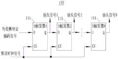
可以理解,所述处理模块100的具体结构不限制,只要具有基于预设时钟信号和预设宽度设置信号对所述待检测特定编码信号的进行处理并输出成型信号的功能即可。在一个实施例中,所述处理模块100可包括缓存模块110、高电平展宽模块120和检测模块130。具体的,如图3所示,所述缓存模块110可包括N个级联的D触发器111。其中,N为大于1的整数,且N大于所述待检测特定编码信号与所述预设时钟信号的周期之比。It can be understood that the specific structure of the
在一个实施例中,所述缓存模块110可由所述预设时钟信号的边沿(即上升沿或下降沿)触发。当所述预设时钟信号输入至所述缓存模块110时,即各级所述D触发器111均接收到所述预设时钟信号的边沿触发信号时,各级所述D触发器111将所述待检测特定编码信号进行移位缓存,同时各级所述D触发器111输出与之对应的延迟的抽头信号。具体如图3所示,各级所述D触发器111均输出与之对应的抽头信号。例如,D触发器1输出抽头信号1,D触发器2输出抽头信号2……D触发器N输出抽头信号N。In one embodiment, the
在一个实施例中,所述高电平展宽模块120的第一输入端与所述缓存模块110的输出端电连接。所述高电平展宽模块120的第二输入端用于输入所述预设宽度设置信号。所述高电平展宽模块120用于根据各级所述抽头信号和所述预设宽度设置信号输出所述成型信号。在一个实施例中,如图4所示,所述高电平展宽模块120可包括多个或门电路121和一选择电路122。在一个实施例中,所述或门电路121可为逻辑或门。In one embodiment, the first input terminal of the high
具体的,多个或门电路121中的任意一个或门电路121的两个输入端分别接收抽头信号1和抽头信号2。其它每个或门电路121的一个输入端与相邻或门电路121的输出端连接、另一个输入端接收一抽头信号,且每个或门电路121接收的抽头信号不相同。多个或门电路121的输出端均与选择电路122电连接,同时选择电路122还可直接接收抽头信号1。例如,或门电路1的一个输入端接收抽头信号1、另一个输入端接收抽头信号2、输出端与选择电路122的输入端2电连接,或门电路2的一个输入端接收抽头信号3、另一个输入端与或门电路1的输出端电连接、或门电路2的输出端与选择电路122的输入端3电连接……或门电路N-1的一个输入端接收抽头信号N、另一个输入端与或门电路N-2的输出端电连接、或门电路N-1的输出端与选择电路122的输入端N电连接。选择电路122的输入端1直接接收抽头信号1。Specifically, the two input terminals of any one of the
在一个实施例中,所述选择电路122还用于接收所述预设宽度设置信号,并根据该预设宽度设置信号确定输出的所述成型信号为各级所述抽头信号中的哪一个。例如,若所述选择电路122接收的所述预设宽度设置信号为3,则所述选择电路122输出端输出的所述成型信号即为所述选择电路122输入端3接收的信号。若所述选择电路122接收的所述预设宽度设置信号为N,则所述选择电路122输出端输出的所述成型信号即为所述选择电路122输入端N接收的信号。在一个实施例中,所述预设宽度设置信号对应的数值应大于所述待检测特定编码信号中高电平脉冲存在的最大长度与所述预设时钟信号的周期之差。在一个实施例中,所述选择电路122为多选一选择器。In one embodiment, the
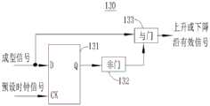
在一个实施例中,所述检测模块130分别与所述高电平展宽模块120、所述计时模块200以及所述计时保持模块300电连接。所述检测模块130用于根据所述预设时钟信号检测所述成型信号的上升或下降沿并输出上升或下降沿有效信号。可以理解,所述检测模块130的具体结构不限制,只要具有测所述成型信号的上升或下降沿并输出上升或下降沿有效信号的功能即可。在一个实施例中,如图5所示,所述检测模块130可由触发器131、非门132以及与门133组成。具体的,所述触发器131的第一输入端与所述高电平展宽模块120的输出端电连接。所述触发器131的第二输入端用于输入所述预设时钟信号。所述非门132的输入端与所述触发器131的输出端电连接。所述与门133的第一输入端与所述高电平展宽模块120的输出端电连接。所述与门133的第二输入端与所述非门132的输出端电连接。所述与门133的输出端用于输出所述上升或下降沿有效信号至所述计时模块200。In one embodiment, the
在一个实施例中,所述触发器131可采用D触发器。在一个实施例中,所述触发器131可由所述预设时钟信号的边沿(即上升沿或下降沿)触发。本实施例通过所述触发器131、所述非门132以及所述与门133配合,可实现对所述成型信号的上升沿或下降沿进行检测,最终输出所述上升或下降沿有效信号至所述计时模块200。In one embodiment, the flip-
在一个实施例中,所述计时模块200可由所述预设时钟信号的边沿(即上升沿或下降沿)触发。当所述检测模块130输出所述上升或下降沿有效信号至所述计时模块200时,所述计时模块200可统计所述成型信号中相邻所述上升或下降沿有效信号对应接收的所述预设时钟信号的周期个数。即所述计时模块200在相邻所述上升或下降沿有效信号对应的时间段,可统计所述计时模块200接收的所述预设时钟信号的周期个数。具体的,在所述成型信号中相邻所述上升或下降沿有效信号对应的时间段,所述计时模块200可对接收的所述预设时钟信号的上升沿或下降沿进行计数,并输出实时计时值。In one embodiment, the
在一个实施例中,所述计时保持模块300可由所述预设时钟信号的边沿(即上升沿或下降沿)触发。当所述计时保持模块300接收的所述上升或下降沿有效信号有效时,所述计时保持模块300可对所述计时模块200输出的所述实时计时值进行采样并保存,此时所述计时模块200自动将所述实时计时值清零,并重新计数。同时所述计时保持模块300将保存后的所述计时保持值输出至所述判断模块400。In one embodiment, the
在一个实施例中,所述判断模块400接收所述计时保持模块300输出的所述计时保持值,并根据所述计时保持值和所述设定阈值确定输出的所述频率判决信号是否为有效。具体的,所述判断模块400对可确定所述计时保持值是否在所述设定阈值范围内。若确定所述计时保持值在所述设定阈值范围内,则所述判断模块400输出的所述频率判决信号为有效。若确定所述计时保持值未在所述设定阈值范围内,则所述判断模块400输出的所述频率判决信号为无效。在一个实施例中,所述设定阈值可根据所述待检测特定编码信号的周期长度设置信号和周期容错设置信号设定。具体的,所述设定阈值的范围可为所述周期长度设置信号与所述周期容错设置信号之差至所述周期长度设置信号与所述周期容错设置信号之和。在一个实施例中,所述周期长度设置信号和所述周期容错设置信号可根据实际需求提前设置在所述判断模块400内。In one embodiment, the judging
在一个实施例中,所述计数处理模块500可由延时器和计数器组成。在一个实施例中,所述计数处理模块500可由所述预设时钟信号的边沿(即上升沿或下降沿)触发。具体的,当所述计数处理模块500被触发后,所述计数处理模块500可在所述上升或下降沿有效信号延迟一个所述预设时钟信号周期后接收所述频率判决信号。若所述计数处理模块500接收的所述频率判决信号为有效信号,则所述计数处理模块500内的计数值累计加1。若所述计数处理模块500接收的所述频率判决信号为无效信号,则所述计数处理模块500内的所述计数值清零。In one embodiment, the
在一个实施例中,所述预设同步头周期数值可提前存储在所述计数处理模块500内。当所述计数处理模块500内的所述计数值累计达到所述预设同步头周期数值,即所述计数值与所述预设同步头周期数值相等时,表明检测到了有效的同步头信号,此时所述计数处理模块500输出的所述频率检测结果为有效。反之,当所述计数值小于所述预设同步头周期数值时,表明未检测到有效的同步头信号,此时所述计数处理模块500输出的所述频率检测结果为无效。In one embodiment, the preset sync header period value may be stored in the
在一个实施例中,当所述计数处理模块500输出的所述频率检测结果为有效时,所述采样时刻生成模块600可判断接收的所述实时计时值是否与所述预设固定值相等。若所述采样时刻生成模块600确定所述实时计时值与所述预设固定值相等,则所述采样时刻生成模块600输出所述采样时刻有效信号。若所述采样时刻生成模块600确定所述实时计时值与所述预设固定值不相等,则所述采样时刻生成模块600不输出所述采样时刻有效信号。其中,所述预设固定值为正整数,一般为1或高电平宽度设置值-1。In one embodiment, when the frequency detection result output by the
在一个实施例中,当所述计数处理模块500输出的所述频率检测结果为无效时,所述采样时刻生成模块600此时不对接收的所述实时计时值是否与所述预设固定值相等进行判断。即只有当所述频率检测结果为有效时,所述采样时刻生成模块600才会对接收的所述实时计时值是否与所述预设固定值相等进行判断。In one embodiment, when the frequency detection result output by the
在一个实施例中,所述编码处理模块700可包括:解码缓存模块710和编码判断模块720。具体的,所述解码缓存模块710分别与所述采样时刻生成模块600和所述处理模块100电连接。所述解码缓存模块710用于基于所述预设时钟信号确定所述采样时刻有效信号是否有效,若所述采样时刻有效信号有效,则将所述成型信号移位缓存并输出缓存接收信号。所述编码判断模块720与所述解码缓存模块710电连接。所述编码判断模块720用于根据所述缓存接收信号和所述预设编码值信号确定输出的编码检测结果是否有效。In one embodiment, the
在一个实施例中,所述解码缓存模块710可由所述预设时钟信号的边沿(即上升沿或下降沿)触发。当所述述采样时刻生成模块600输出所述采样时刻有效信号时,所述解码缓存模块710可判断接收的所述采样时刻有效信号是否有效。若所述采样时刻有效信号为有效,则将所述成型信号移位缓存并输出缓存接收信号至所述编码判断模块720。反之,若所述采样时刻有效信号为无效(即所述解码缓存模块710未接收到所述采样时刻有效信号时),则所述解码缓存模块710不对所述成型信号进行移位缓存。在一个实施例中,所述解码缓存模块710可包括N个D触发器;其中,N为大于或等于所述预设编码值信号的比特位数。In one embodiment, the
在一个实施例中,所述编码判断模块720接收到所述解码缓存模块710发送的所述缓存接收信号后,可将该所述缓存接收信号与所述预设编码值信号进行比较。若所述缓存接收信号与所述预设编码值信号相同,表明所述特定编码信号的检测电路10检测到了有效的特定编码信号,则所述编码判断模块720输出的所述编码检测结果为有效。反之,若所述缓存接收信号与所述预设编码值信号不相同,表明所述特定编码信号的检测电路10未检测到有效的特定编码信号,则所述编码判断模块720输出的所述编码检测结果为无效。In one embodiment, after the
采用上述检测电路可实现对特定编码信号的低功耗检测。其可作为解调和解码电路应用在需要无线低功耗唤醒功能的电路中,如物联网和车联网中的无线传感器端设计领域。The low power consumption detection of a specific coded signal can be realized by adopting the above detection circuit. It can be used as a demodulation and decoding circuit in circuits that require wireless low-power wake-up functions, such as the wireless sensor end design field in the Internet of Things and the Internet of Vehicles.
本实施例中,通过处理模块100基于预设时钟信号和预设宽度设置信号对待检测特定编码信号进行处理并输出成型信号,同时检测该成型信号的上升或下降沿并输出上升或下降沿有效信号;通过计时模块200统计所述成型信号中相邻所述上升或下降沿有效信号对应接收的所述预设时钟信号的周期个数,并与计时保持模块300配合输出计时保持值至判断模块400,从而确定频率判决信号是否为有效;并通过计数处理模块500根据所述频率判决信号和预设同步头周期数值确定输出的频率检测结果是否有效。当频率检测结果有效时,通过采样时刻生成模块600基于所述实时计时值和预设固定值确定是否输出采样时刻有效信号至编码处理模块;最后通过编码处理模块700基于所述预设时钟信号、所述采样时刻有效信号和预设编码值信号确定输出的编码检测结果是否有效,从而实现对特定编码信号的低功耗检测功能。In this embodiment, the
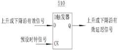
在一个实施例中,所述计数处理模块500包括延迟模块510以及计数模块520。所述延迟模块510与所述处理模块100电连接。所述延迟模块510用于基于所述预设时钟信号将所述上升或下降沿有效信号延迟一个所述预设时钟信号周期,并输出上升或下降沿有效延迟信号。所述计数模块520分别与所述判断模块400和所述延迟模块510电连接。所述计数模块520用于基于所述预设时钟信号在所述上升或下降沿有效延迟信号有效时接收所述频率判决信号,并根据所述频率判决信号是否有效和所述预设同步头周期数值确定输出的所述频率检测结果是否有效。In one embodiment, the
在一个实施例中,所述延迟模块510和所述计数模块520均可由所述预设时钟信号的边沿(即上升沿或下降沿)进行触发。在一个实施例中,当所述延迟模块510被所述预设时钟信号触发后,所述延迟模块510可将所述处理模块100中的所述检测模块130输出的所述上升或下降沿有效信号延迟一个所述预设时钟信号周期并输出上升或下降沿有效延迟信号至所述计数模块520。其中,如图6所示,所述延迟模块510可由D触发器构成。In one embodiment, both the
当所述计数模块520被所述预设时钟信号触发后,所述计数模块520可在所述上升或下降沿有效延迟信号有效时接收所述频率判决信号,若所述计数模块520接收的所述频率判决信号为有效信号,则所述计数模块520内的计数值累计加1。若所述计数模块520接收的所述频率判决信号为无效信号,则所述计数模块520内的所述计数值清零。After the
当所述计数模块520内的所述计数值累计达到所述预设同步头周期数值,即所述计数值与所述预设同步头周期数值相等时,表明所述特定编码信号的检测电路10检测到了有效的同步头信号,此时所述计数模块520输出的所述频率检测结果为有效。反之,当所述计数值小于所述预设检测周期数值时,表明所述特定编码信号的检测电路10未检测到有效的同步头信号,此时所述计数模块520输出的所述频率检测结果为为无效。When the count value accumulated in the
因所述缓存模块110、所述检测模块130、所述计时模块200、所述计时保持模块300、所述延迟模块510、所述计数模块520以及所述解码缓存模块710均采用所述预设时钟信号进行唤醒,可使得所述特定编码信号的检测电路10在检测特定编码信号时,降低功耗,从而可实现对特定编码信号的低功耗检测功能。Because the
在一个实施例中,所述计数模块520与所述计时模块200电连接。所述计时模块200还用于确定所述实时计时值是否超过其最大可计数范围。若所述实时计时值超过所述最大可计数范围,则此时所述计时模块200分别输出计时值无效信号至所述计时保持模块300和所述计数模块520,同时所述计时模块200将所述实时计时值清零。而所述计时保持模块300在接收到所述计时值无效信号时,所述计时保持模块300将保存的所述计时保持值清零。与此同时,当所述计数模块520接收到所述计时值无效信号时,则所述计数模块520也将所述计数值清零。即只要所述计时模块200确定所述实时计时值超过所述最大可计数范围,则所述计时模块200、所述计时保持模块300以及所述计数模块520均将各自的计数清零。In one embodiment, the
在一个实施例中,当所述计数模块520输出的所述频率检测结果为有效时,所述计时模块200基于预设周期长度将所述实时计时值清零并重新在所述预设周期长度内计数。具体的,当所述频率检测结果为有效时,所述计时模块200可在所述预设周期长度内对接收的所述预设时钟信号的周期个数进行实时计数,并输出实时计时值。当达到所述预设周期长度时,所述计时模块200将所述实时计时值清零,并重新在所述预设周期长度内对接收的所述预设时钟信号的周期个数进行计数。In one embodiment, when the frequency detection result output by the
综上所述,本申请通过处理模块100基于预设时钟信号和预设宽度设置信号对待检测特定编码信号进行处理并输出成型信号,同时检测该成型信号的上升或下降沿并输出上升或下降沿有效信号;通过计时模块200统计所述成型信号中相邻所述上升或下降沿有效信号对应接收的所述预设时钟信号的周期个数,并与计时保持模块300配合输出计时保持值至判断模块400,从而确定频率判决信号是否为有效;并通过计数处理模块500根据所述频率判决信号和预设同步头周期数值确定输出的频率检测结果是否有效。当频率检测结果有效时,通过采样时刻生成模块600基于所述实时计时值和预设固定值确定是否输出采样时刻有效信号至编码处理模块;最后通过编码处理模块700基于所述预设时钟信号、所述采样时刻有效信号和预设编码值信号确定输出的编码检测结果是否有效,从而实现对特定编码信号的低功耗检测功能。In summary, the present application uses the
以上所述实施例的各技术特征可以进行任意的组合,为使描述简洁,未对上述实施例中的各个技术特征所有可能的组合都进行描述,然而,只要这些技术特征的组合不存在矛盾,都应当认为是本说明书记载的范围。The technical features of the above-mentioned embodiments can be combined arbitrarily. To make the description concise, all possible combinations of the technical features in the above-mentioned embodiments are not described. However, as long as there is no contradiction in the combination of these technical features, should be considered as within the scope of this specification.
以上所述实施例仅表达了本申请的几种实施方式,其描述较为具体和详细,但并不能因此而理解为对发明专利范围的限制。应当指出的是,对于本领域的普通技术人员来说,在不脱离本申请构思的前提下,还可以做出若干变形和改进,这些都属于本申请的保护范围。因此,本申请专利的保护范围应以所附权利要求为准。The above-mentioned embodiments only represent several implementation modes of the present application, and the description thereof is relatively specific and detailed, but it should not be construed as limiting the scope of the patent for the invention. It should be noted that those skilled in the art can make several modifications and improvements without departing from the concept of the present application, and these all belong to the protection scope of the present application. Therefore, the scope of protection of the patent application should be based on the appended claims.
Claims (10)
Translated fromChinesePriority Applications (1)
| Application Number | Priority Date | Filing Date | Title |
|---|---|---|---|
| CN202010492407.6ACN111817703B (en) | 2020-06-03 | 2020-06-03 | Detection circuit for specific coded signal |
Applications Claiming Priority (1)
| Application Number | Priority Date | Filing Date | Title |
|---|---|---|---|
| CN202010492407.6ACN111817703B (en) | 2020-06-03 | 2020-06-03 | Detection circuit for specific coded signal |
Publications (2)
| Publication Number | Publication Date |
|---|---|
| CN111817703A CN111817703A (en) | 2020-10-23 |
| CN111817703Btrue CN111817703B (en) | 2023-04-14 |
Family
ID=72847858
Family Applications (1)
| Application Number | Title | Priority Date | Filing Date |
|---|---|---|---|
| CN202010492407.6AActiveCN111817703B (en) | 2020-06-03 | 2020-06-03 | Detection circuit for specific coded signal |
Country Status (1)
| Country | Link |
|---|---|
| CN (1) | CN111817703B (en) |
Families Citing this family (1)
| Publication number | Priority date | Publication date | Assignee | Title |
|---|---|---|---|---|
| CN114043827B (en)* | 2021-11-16 | 2023-09-29 | 南京英锐创电子科技有限公司 | Tire pressure signal processing method and device |
Citations (6)
| Publication number | Priority date | Publication date | Assignee | Title |
|---|---|---|---|---|
| DE2052600A1 (en)* | 1970-10-27 | 1972-05-10 | Fernseh Gmbh | Pulse width discriminator |
| CN101510766A (en)* | 2008-02-14 | 2009-08-19 | 精工电子有限公司 | Method of fabricating piezoelectric vibrating piece, wafer, apparatus having the piezoelectric vibrating piece |
| CN201589820U (en)* | 2010-01-11 | 2010-09-22 | 中色科技股份有限公司 | Simple and easy detection equipment for measuring three-phase alternating current phase sequence |
| CN108321770A (en)* | 2017-12-29 | 2018-07-24 | 奥克斯空调股份有限公司 | A kind of multiphase phase sequence switching device and method |
| CN109121445A (en)* | 2016-02-05 | 2019-01-01 | Oppo广东移动通信有限公司 | Anti- guard method and power supply adaptor when charging system, charging |
| CN110632397A (en)* | 2019-08-30 | 2019-12-31 | 深圳市华奥通通信技术有限公司 | Signal analysis method and computer readable storage medium |
- 2020
- 2020-06-03CNCN202010492407.6Apatent/CN111817703B/enactiveActive
Patent Citations (6)
| Publication number | Priority date | Publication date | Assignee | Title |
|---|---|---|---|---|
| DE2052600A1 (en)* | 1970-10-27 | 1972-05-10 | Fernseh Gmbh | Pulse width discriminator |
| CN101510766A (en)* | 2008-02-14 | 2009-08-19 | 精工电子有限公司 | Method of fabricating piezoelectric vibrating piece, wafer, apparatus having the piezoelectric vibrating piece |
| CN201589820U (en)* | 2010-01-11 | 2010-09-22 | 中色科技股份有限公司 | Simple and easy detection equipment for measuring three-phase alternating current phase sequence |
| CN109121445A (en)* | 2016-02-05 | 2019-01-01 | Oppo广东移动通信有限公司 | Anti- guard method and power supply adaptor when charging system, charging |
| CN108321770A (en)* | 2017-12-29 | 2018-07-24 | 奥克斯空调股份有限公司 | A kind of multiphase phase sequence switching device and method |
| CN110632397A (en)* | 2019-08-30 | 2019-12-31 | 深圳市华奥通通信技术有限公司 | Signal analysis method and computer readable storage medium |
Non-Patent Citations (1)
| Title |
|---|
| 一种小型脉冲激光器能量和重复频率测量电路;侯宏录 等;《兵工自动化》;20140930;第33卷(第9期);第76-79页* |
Also Published As
| Publication number | Publication date |
|---|---|
| CN111817703A (en) | 2020-10-23 |
Similar Documents
| Publication | Publication Date | Title |
|---|---|---|
| KR102205823B1 (en) | Clock recovery circuit for multiple wire data signals | |
| US6008746A (en) | Method and apparatus for decoding noisy, intermittent data, such as manchester encoded data or the like | |
| CN105897639A (en) | FSK demodulator | |
| CN101286735B (en) | Delay device of reset signal | |
| TWI407696B (en) | Asynchronous ping-pong counter | |
| CN1983225A (en) | Device and method for transmitting data in asynchronous clock domain | |
| CN111817703B (en) | Detection circuit for specific coded signal | |
| JP2012142889A (en) | Communication circuit and sampling adjustment method | |
| CN107911102B (en) | Synchronous filter and method for cross-clock domain asynchronous data | |
| CN113282531B (en) | Two-port serial data transceiver circuit and method based on pulse trigger | |
| CN104065361B (en) | A kind of serially concatenated single-bit filter construction for eliminating burr signal | |
| JP4349866B2 (en) | FSK signal demodulation circuit | |
| CN111830330B (en) | Detection circuit for specific frequency signal | |
| CN111211774A (en) | Bounce removing circuit | |
| EP3846380A1 (en) | Clock and data recovery circuit | |
| TWI425878B (en) | Driving circuit of light emitting diode | |
| CN100498863C (en) | Variable length coding method and circuit thereof | |
| CN210201839U (en) | Transmission protocol self-adaptive decoding system | |
| CN115242932A (en) | A Companion Clock-Based Training Method with Low Resource Occupancy | |
| CN101751357B (en) | Digital phase-locked loop device | |
| CN109525241B (en) | Gray code counter | |
| US7233636B2 (en) | Technique for oversampling to reduce jitter | |
| CN106127280B (en) | A kind of TPP decoding circuit based on UHF RFID chip | |
| CN106950871B (en) | Microcontroller and timing counter thereof | |
| TWI662529B (en) | Parallel bus device of led display unit board |
Legal Events
| Date | Code | Title | Description |
|---|---|---|---|
| PB01 | Publication | ||
| PB01 | Publication | ||
| SE01 | Entry into force of request for substantive examination | ||
| SE01 | Entry into force of request for substantive examination | ||
| GR01 | Patent grant | ||
| GR01 | Patent grant | ||
| CP03 | Change of name, title or address | Address after:Floor 14, Building A, Chuangzhi Building, No. 17 Xinghuo Road, Jiangbei New District, Nanjing, Jiangsu Province, 211800 Patentee after:Wanjie Electronic Technology (Jiangsu) Co.,Ltd. Country or region after:China Address before:14th Floor, Building A, Chuangzhi Building, No. 17 Xinghuo Road, Jiangbei New District, Nanjing City, Jiangsu Province Patentee before:Nanjing yingruichuang Electronic Technology Co.,Ltd. Country or region before:China | |
| CP03 | Change of name, title or address |