CN111814498A - Microelectromechanical fluid device chip - Google Patents
Microelectromechanical fluid device chipDownload PDFInfo
- Publication number
- CN111814498A CN111814498ACN201910293653.6ACN201910293653ACN111814498ACN 111814498 ACN111814498 ACN 111814498ACN 201910293653 ACN201910293653 ACN 201910293653ACN 111814498 ACN111814498 ACN 111814498A
- Authority
- CN
- China
- Prior art keywords
- identification circuit
- device chip
- mems device
- chip
- control electrodes
- Prior art date
- Legal status (The legal status is an assumption and is not a legal conclusion. Google has not performed a legal analysis and makes no representation as to the accuracy of the status listed.)
- Pending
Links
Images


Classifications
- G—PHYSICS
- G06—COMPUTING OR CALCULATING; COUNTING
- G06K—GRAPHICAL DATA READING; PRESENTATION OF DATA; RECORD CARRIERS; HANDLING RECORD CARRIERS
- G06K7/00—Methods or arrangements for sensing record carriers, e.g. for reading patterns
- B—PERFORMING OPERATIONS; TRANSPORTING
- B81—MICROSTRUCTURAL TECHNOLOGY
- B81B—MICROSTRUCTURAL DEVICES OR SYSTEMS, e.g. MICROMECHANICAL DEVICES
- B81B7/00—Microstructural systems; Auxiliary parts of microstructural devices or systems
- B81B7/02—Microstructural systems; Auxiliary parts of microstructural devices or systems containing distinct electrical or optical devices of particular relevance for their function, e.g. microelectro-mechanical systems [MEMS]
Landscapes
- Engineering & Computer Science (AREA)
- Artificial Intelligence (AREA)
- Computer Vision & Pattern Recognition (AREA)
- Physics & Mathematics (AREA)
- General Physics & Mathematics (AREA)
- Theoretical Computer Science (AREA)
- Computer Hardware Design (AREA)
- Microelectronics & Electronic Packaging (AREA)
- Micromachines (AREA)
Abstract
Description
Translated fromChinese技术领域technical field
本案是关于一种微机电流体装置芯片,尤指一种包含识别电路的微机电流体装置芯片。This case is about a microelectromechanical fluid device chip, especially a microelectromechanical fluid device chip including an identification circuit.
背景技术Background technique
随着科技的日新月异,传统的流体输送装置已朝向装置微小化、流量极大化的方向进行。在应用上也愈来愈多元化,举凡工业应用、生医应用、医疗保健、电子散热到近来热门的穿戴式装置皆可见它的踪影。With the rapid development of science and technology, the traditional fluid delivery device has moved towards the miniaturization of the device and the maximization of the flow. Its applications are also becoming more and more diversified. It can be seen in industrial applications, biomedical applications, medical care, electronic cooling, and recently popular wearable devices.
综观现行的微机电流体装置应用技术日趋复杂,而各种微机电流体装置皆有其特定规格(如使用电压、驱动信号、控制方式…等),需搭配相容的驱动系统,才能正确地完成工作,故需要一特定电路元件作为驱动系统识别微机电流体装置特性或信息之用。Looking at the current application technology of MEMS devices is becoming more and more complex, and various MEMS devices have their specific specifications (such as voltage, driving signal, control method, etc.) Therefore, a specific circuit element is required for the drive system to identify the characteristics or information of the MEMS device.
发明内容SUMMARY OF THE INVENTION
本案的目的在于提供一种微机电流体装置芯片,包含一识别电路,识别电路用以记录微机电流体装置信息并透过电子电路提供给驱动系统信息,使驱动系统与微机电流体装置芯片之间有良好的搭配,并借此达到识别微机电流体装置芯片的目的。The purpose of this application is to provide a microelectromechanical fluid device chip, including an identification circuit, the identification circuit is used to record the information of the microelectromechanical fluid device and provide the information to the driving system through the electronic circuit, so as to make the connection between the driving system and the microelectromechanical fluid device chip There is a good match, and the purpose of identifying the microelectromechanical fluid device chip is achieved thereby.
为达上述目的,本案的较广义实施态样为提供一种微机电流体装置芯片,包含一芯片本体、多个微机电流体装置以及一识别电路。芯片本体是一长方体态样,具有二长边以及二短边。微机电流体装置设置于芯片本体上。识别电路与芯片本体电性连接,并包含多个保险丝、多个第一控制电极以及多个第二控制电极。每一保险丝的两端分别与相对应的第一控制电极以及第二控制电极相连接。借由提供一高电压给至少一保险丝,使得至少一保险丝熔断,借以识别微机电流体装置芯片。In order to achieve the above purpose, a broader implementation aspect of the present application is to provide a microelectromechanical fluid device chip, which includes a chip body, a plurality of microelectromechanical fluid devices, and an identification circuit. The chip body is a rectangular parallelepiped with two long sides and two short sides. The microelectromechanical fluid device is arranged on the chip body. The identification circuit is electrically connected to the chip body, and includes a plurality of fuses, a plurality of first control electrodes and a plurality of second control electrodes. Two ends of each fuse are respectively connected with the corresponding first control electrode and the second control electrode. By supplying a high voltage to the at least one fuse, the at least one fuse is blown, so as to identify the microelectromechanical fluid device chip.
附图说明Description of drawings
为让本发明的上述目的、特征和优点能更明显易懂,以下结合附图对本发明的具体实施方式作详细说明,其中:In order to make the above-mentioned objects, features and advantages of the present invention more obvious and easy to understand, the specific embodiments of the present invention are described in detail below in conjunction with the accompanying drawings, wherein:
图1A为本案微机电流体装置芯片的第一实施例的示意图。FIG. 1A is a schematic diagram of the first embodiment of the microelectromechanical fluid device chip of the present invention.
图1B为本案微机电流体装置芯片的第二实施例的示意图。FIG. 1B is a schematic diagram of a second embodiment of the microelectromechanical fluid device chip of the present invention.
图1C为本案微机电流体装置芯片的第三实施例的示意图。FIG. 1C is a schematic diagram of a third embodiment of the microelectromechanical fluid device chip of the present invention.
图1D为本案微机电流体装置芯片的第四实施例的示意图。FIG. 1D is a schematic diagram of the fourth embodiment of the microelectromechanical fluid device chip of the present invention.
图2A以及图2B为本案识别电路的第一实施态样的示意图。FIG. 2A and FIG. 2B are schematic diagrams of the first embodiment of the identification circuit of the present invention.
图3A以及图3B为本案识别电路的第二实施态样的示意图。3A and 3B are schematic diagrams of a second implementation of the identification circuit of the present invention.
图4A以及图4B为本案识别电路的第三实施态样的示意图。4A and 4B are schematic diagrams of a third embodiment of the identification circuit of the present invention.
图5A以及图5B为本案识别电路的第四实施态样的示意图。FIG. 5A and FIG. 5B are schematic diagrams of a fourth implementation aspect of the identification circuit of the present invention.
图中元件标号说明:Description of component numbers in the figure:
1a、1b、1c、1d:微机电流体装置芯片1a, 1b, 1c, 1d: Microelectromechanical fluid device chips
10:芯片本体10: Chip body
10a:长边10a: Long side
10b:短边10b: Short side
11:微机电流体装置11: MEMS Fluid Devices
12、12a、12b、12c、12d:识别电路12, 12a, 12b, 12c, 12d: Identification circuits
F1、F2、F3、F4、F5:保险丝F1, F2, F3, F4, F5: Fuse
PD:集合电极PD: Collector electrode
P1a、P2a、P3a、P4a、P5a:第一控制电极P1a, P2a, P3a, P4a, P5a: first control electrode
P1b、P2b、P3b、P4b、P5b:第二控制电极P1b, P2b, P3b, P4b, P5b: second control electrodes
M1、M2、M3、M4、M5:场效晶体管M1, M2, M3, M4, M5: Field Effect Transistors
具体实施方式Detailed ways
体现本案特征与优点的实施例将在后段的说明中详细叙述。应理解的是本案能够在不同的态样上具有各种的变化,其皆不脱离本案的范围,且其中的说明及附图在本质上当作说明之用,而非用以限制本案。Embodiments embodying the features and advantages of the present case will be described in detail in the description of the latter paragraph. It should be understood that the present case can have various changes in different aspects without departing from the scope of the present case, and the descriptions and drawings therein are essentially used for illustration rather than limiting the present case.
请参阅图1A,于本案第一实施例中,微机电流体装置芯片1a包含一芯片本体10、多个微机电流体装置11以及一识别电路12。芯片本体10是一长方体态样,具有二长边10a以及二短边10b。微机电流体装置11设置于芯片本体10上,并沿着微机电流体装置芯片1a的长边10a的延伸方向设置。值得注意的是,微机电流体装置11的设置方式于其他实施例中可依设计需求而变更,不以此为限。识别电路12与芯片本体10电性连接,设置于邻近芯片本体10的其中一短边10b处。Please refer to FIG. 1A , in the first embodiment of the present application, the MEMS
请参阅图1B,于本案第二实施例中,微机电流体装置芯片1b的结构类似于本案第一实施例的微机电流体装置芯片1a,其中相同的元件标号代表相似的元件结构与功能,于此不再赘述。不同之处在于,微机电流体装置芯片1b包含二识别电路12,分别对称设置于邻近芯片本体10的二短边10b处。Please refer to FIG. 1B , in the second embodiment of the present application, the structure of the
请参阅图1C,于本案第三实施例中,微机电流体装置芯片1c的结构类似于本案第二实施例的微机电流体装置芯片1b,其中相同的元件标号代表相似的元件结构与功能,于此不再赘述。不同之处在于,二识别电路12分别对称设置于邻近芯片本体10的二长边10a处。Please refer to FIG. 1C , in the third embodiment of the present application, the structure of the MEMS device chip 1c is similar to that of the
请参阅图1D,于本案第四实施例中,微机电流体装置芯片1d的结构类似于本案第一实施例的微机电流体装置芯片1a,其中相同的元件标号代表相似的元件结构与功能,于此不再赘述。不同之处在于,识别电路12设置于芯片本体10的外侧,仅与芯片本体10电性连接。Referring to FIG. 1D, in the fourth embodiment of the present application, the structure of the
值得注意的是,识别电路12的数量以及识别电路12与芯片本体10之间的设置关系,不以本案所公开为限,可依设计需求而变更。It should be noted that the number of the
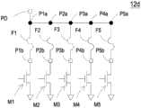
请参阅图2A以及图2B,于本案各实施例中,识别电路12a为识别电路12的第一实施态样,包含多个保险丝F1、F2、F3、F4、F5、多个第一控制电极P1a、P2a、P3a、P4a、P5a以及多个第二控制电极P1b、P2b、P3b、P4b、P5b。每一保险丝F1、F2、F3、F4、F5的两端分别与相对应的第一控制电极P1a、P2a、P3a、P4a、P5a以及第二控制电极P1b、P2b、P3b、P4b、P5b相连接;例如,保险丝F1的两端分别与第一控制电极P1a以及第二控制电极P1b相连接。借此,第一控制电极P1a以及第二控制电极P1b之间形成一回路,借由提供一高电压给保险丝F1,使得保险丝F1熔断,借以识别微机电流体装置芯片1a、1b、1c、1d。如图2A所示,识别电路12a包含五个保险丝F1、F2、F3、F4、F5、五个第一控制电极P1a、P2a、P3a、P4a、P5a以及五个第二控制电极P1b、P2b、P3b、P4b、P5b,但不以此为限。如图2B所示,保险丝F1、F3被熔断形成断路(以虚线表示),而保险丝F2、F4、F5未被熔断而形成回路,借此提供外部控制单元(图未示)一辨别信息来辨别微机电流体装置芯片1a、1b、1c、1d。Please refer to FIG. 2A and FIG. 2B. In each embodiment of the present application, the
请参阅图3A以及图3B,于本案各实施例中,识别电路12b为识别电路12的第二实施态样。识别电路12b与第一实施态样的识别电路12a不同之处在于识别电路12b还包含一集合电极PD,并且集合电极PD与第一控制电极P1a、P2a、P3a、P4a、P5a电性连接。如图3A所示,识别电路12b包含五个保险丝F1、F2、F3、F4、F5、五个第一控制电极P1a、P2a、P3a、P4a、P5a以及五个第二控制电极P1b、P2b、P3b、P4b、P5b,但不以此为限。如图3B所示,保险丝F1、F3被熔断形成断路(以虚线表示),而保险丝F2、F4、F5未被熔断而形成回路,借此辨别微机电流体装置芯片1a、1b、1c、1d。Please refer to FIG. 3A and FIG. 3B , in each embodiment of the present application, the
请参阅图4A以及图4B,于本案各实施例中,识别电路12c为识别电路12的第三实施态样。识别电路12c与第一实施态样的识别电路12a不同之处在于识别电路12c还包含多个场效晶体管M1、M2、M3、M4、M5,分别与第二控制电极P1b、P2b、P3b、P4b、P5b电性连接。如图4A所示,识别电路12c包含五个保险丝F1、F2、F3、F4、F5、五个第一控制电极P1a、P2a、P3a、P4a、P5a、五个第二控制电极P1b、P2b、P3b、P4b、P5b以及五个场效晶体管M1、M2、M3、M4、M5,但不以此为限。于本案各实施例中,场效晶体管M1、M2、M3、M4、M5分别为一N型金属氧化物半导体场效晶体管(NMOS),但不以此为限。如图4B所示,保险丝F1、F3被熔断形成断路(以虚线表示),而保险丝F2、F4、F5未被熔断而形成回路,借此辨别微机电流体装置芯片1a、1b、1c、1d。进行识别电路烧录时,借由导通场效晶体管M1、M3提供一烧录电压给第一控制电极P1a、P3a,使得保险丝F1、F3熔断成断路状态,反之,场效晶体管M2、M4、M5未导通而提供烧录电压给第一控制电极P2a、P4a、P5a,则保险丝F2、F4、F5则不会被熔断而形成回路状态。进行识别电路读取时,保险丝F1、F3已成断路状态,当第一控制电极P1a提供一读取电压,则因保险丝F1为断路状态,第一控制电极P1a的电压会维持在读取电压。当场效晶体管M2为导通状态时,第一控制电极P2a提供读取电压,则因保险丝F2为回路状态,第一控制电极P2a的电压会转变为一低电压。同样地,第一控制电极P3a的电压会维持在读取电压,以及第一控制电极P4a与第一控制电极P5a的电压会转变为低电压。Please refer to FIG. 4A and FIG. 4B , in each embodiment of the present application, the
请参阅图5A以及图5B,于本案各实施例中,识别电路12d为识别电路12的第四实施态样。识别电路12d与第三实施态样的识别电路12c不同之处在于识别电路12d还包含集合电极PD,并且集合电极PD与第一控制电极P1a、P2a、P3a、P4a、P5a电性连接。第四实施态样的烧录以及读取方式与第三实施态样相同,故于此不加以赘述。Please refer to FIG. 5A and FIG. 5B , in each embodiment of the present application, the
值得注意的是,保险丝F1、F2、F3、F4、F5的熔断也可以用于记录微机电流体装置芯片1a、1b、1c、1d的作动时间或是已提供的总流量,借以提醒使用者微机电流体装置芯片1a、1b、1c、1d的使用寿命。It is worth noting that the blowing of the fuses F1, F2, F3, F4, and F5 can also be used to record the actuation time of the
值得注意的是,识别电路的组成不以本案公开为限,除了纯粹由保险丝组成、以及由保险丝及金属氧化物半导体场效晶体管(MOS)组成,亦可以由保险丝、可擦除可编程式只读存储器(EPROM)及金属氧化物半导体场效晶体管(MOS)组成,或由电子式可擦除可编程式只读存储器(EEPROM)配合其他电子元件所组成,但不以此为限,识别电路的组成可依设计需求而变更。此外,可擦除可编程式只读存储器(EPROM)以及子式可擦除可编程式只读存储器(EEPROM)的设置是用以储存电路相关信息。It is worth noting that the composition of the identification circuit is not limited to the disclosure of this case. In addition to being composed of fuses, fuses and metal oxide semiconductor field effect transistors (MOS), it can also be composed of fuses, erasable programmable Read memory (EPROM) and metal oxide semiconductor field effect transistor (MOS), or composed of electronically erasable programmable read-only memory (EEPROM) with other electronic components, but not limited to this, the identification circuit The composition can be changed according to design requirements. In addition, erasable programmable read only memory (EPROM) and sub-type erasable programmable read only memory (EEPROM) are provided for storing circuit related information.
值得注意的是,因识别电路可以用以储存微机电流体装置芯片所需的控制方式,一控制电路或是一微控制器(MCU)可产生信号给各别的微机电流体装置芯片,使各别的微机电流体装置芯片产生相对应的流率、气压以及扬程。It is worth noting that since the identification circuit can be used to store the control mode required by the MEMS device chip, a control circuit or a microcontroller (MCU) can generate signals to the respective MEMS device chips, so that each Other MEMS device chips generate the corresponding flow rate, air pressure and head.
综上所述,本案提供一种微机电流体装置芯片,包含一识别电路,识别电路用以记录微机电流体装置信息并透过电子电路提供给驱动系统信息,使驱动系统与微机电流体装置芯片之间有良好的搭配,并借此达到识别微机电流体装置芯片的目的。To sum up, the present application provides a MEMS device chip, which includes an identification circuit, and the identification circuit is used to record the information of the MEMS device and provide the information to the driving system through the electronic circuit, so that the driving system and the MEMS device chip can be connected with each other. There is a good match between them, and the purpose of identifying the microelectromechanical fluid device chip is achieved thereby.
虽然本发明已以较佳实施例揭示如上,然其并非用以限定本发明,任何本领域技术人员,在不脱离本发明的精神和范围内,当可作些许的修改和完善,因此本发明的保护范围当以权利要求书所界定的为准。Although the present invention has been disclosed above with preferred embodiments, it is not intended to limit the present invention. Any person skilled in the art can make some modifications and improvements without departing from the spirit and scope of the present invention. Therefore, the present invention The scope of protection shall be defined by the claims.
Claims (10)
Translated fromChinesePriority Applications (1)
| Application Number | Priority Date | Filing Date | Title |
|---|---|---|---|
| CN201910293653.6ACN111814498A (en) | 2019-04-12 | 2019-04-12 | Microelectromechanical fluid device chip |
Applications Claiming Priority (1)
| Application Number | Priority Date | Filing Date | Title |
|---|---|---|---|
| CN201910293653.6ACN111814498A (en) | 2019-04-12 | 2019-04-12 | Microelectromechanical fluid device chip |
Publications (1)
| Publication Number | Publication Date |
|---|---|
| CN111814498Atrue CN111814498A (en) | 2020-10-23 |
Family
ID=72843724
Family Applications (1)
| Application Number | Title | Priority Date | Filing Date |
|---|---|---|---|
| CN201910293653.6APendingCN111814498A (en) | 2019-04-12 | 2019-04-12 | Microelectromechanical fluid device chip |
Country Status (1)
| Country | Link |
|---|---|
| CN (1) | CN111814498A (en) |
Citations (7)
| Publication number | Priority date | Publication date | Assignee | Title |
|---|---|---|---|---|
| KR19990018176A (en)* | 1997-08-26 | 1999-03-15 | 윤종용 | Redundancy Selection Circuit of Semiconductor Memory Device |
| CN1318866A (en)* | 2000-04-20 | 2001-10-24 | 株式会社东芝 | Multi-chip semiconductor device and storage card |
| CN1533893A (en)* | 2003-03-28 | 2004-10-06 | 国际联合科技股份有限公司 | Recording device for identification circuit of ink-jet printing head |
| CN101034246A (en)* | 2006-03-07 | 2007-09-12 | 上海信诚至典网络技术有限公司 | Projector for automatic recognition of suspended ceiling model |
| CN104228347A (en)* | 2013-06-18 | 2014-12-24 | 研能科技股份有限公司 | Ink jet head chip |
| TWM576619U (en)* | 2018-12-05 | 2019-04-11 | 研能科技股份有限公司 | Micro electrical-mechanical pump module |
| CN209674377U (en)* | 2019-04-12 | 2019-11-22 | 研能科技股份有限公司 | Microelectromechanical fluid device chip |
- 2019
- 2019-04-12CNCN201910293653.6Apatent/CN111814498A/enactivePending
Patent Citations (8)
| Publication number | Priority date | Publication date | Assignee | Title |
|---|---|---|---|---|
| KR19990018176A (en)* | 1997-08-26 | 1999-03-15 | 윤종용 | Redundancy Selection Circuit of Semiconductor Memory Device |
| CN1318866A (en)* | 2000-04-20 | 2001-10-24 | 株式会社东芝 | Multi-chip semiconductor device and storage card |
| US20010045645A1 (en)* | 2000-04-20 | 2001-11-29 | Kabushiki Kaisha Toshiba | Multichip semiconductor device and memory card |
| CN1533893A (en)* | 2003-03-28 | 2004-10-06 | 国际联合科技股份有限公司 | Recording device for identification circuit of ink-jet printing head |
| CN101034246A (en)* | 2006-03-07 | 2007-09-12 | 上海信诚至典网络技术有限公司 | Projector for automatic recognition of suspended ceiling model |
| CN104228347A (en)* | 2013-06-18 | 2014-12-24 | 研能科技股份有限公司 | Ink jet head chip |
| TWM576619U (en)* | 2018-12-05 | 2019-04-11 | 研能科技股份有限公司 | Micro electrical-mechanical pump module |
| CN209674377U (en)* | 2019-04-12 | 2019-11-22 | 研能科技股份有限公司 | Microelectromechanical fluid device chip |
Non-Patent Citations (2)
| Title |
|---|
| "泰科电子推出1206封装额定大电流快断式片状保险丝", 电源技术应用, no. 03, 15 March 2009 (2009-03-15), pages 85* |
| 王兆义 主编: "《电工电子技术基础》", 30 June 2006, 高等教育出版社, pages: 167 - 170* |
Similar Documents
| Publication | Publication Date | Title |
|---|---|---|
| TWI641115B (en) | Memory unit and memory array | |
| TWI420527B (en) | Nonvolatile memory device | |
| CN101556828B (en) | Nonvolatile memory device unit cell and nonvolatile memory device having the same | |
| TWI553645B (en) | Non-volatile memory and its row decoder | |
| CN101246747A (en) | One-time programmable unit and storage device having the unit | |
| US10348085B2 (en) | Static electricity protection circuit, semiconductor integrated circuit device, and electronic apparatus | |
| CN107229881A (en) | Sram-Based Authentication Circuit | |
| CN106158018A (en) | Non-volatile memory cell structure and device thereof | |
| CN209674377U (en) | Microelectromechanical fluid device chip | |
| US6944056B2 (en) | Semiconductor non-volatile storage device | |
| CN111814498A (en) | Microelectromechanical fluid device chip | |
| CN103328932B (en) | SIC (semiconductor integrated circuit) and semiconductor physical quantity sensor device | |
| TWI720457B (en) | Micro-electromechanical system fluid device chip | |
| JP6430306B2 (en) | Nonvolatile memory device | |
| JP6264160B2 (en) | Semiconductor physical quantity sensor device | |
| TWM582042U (en) | Microelectromechanical fluid device chip | |
| CN111366874B (en) | Leakage detection circuit, flash memory leakage detection device and leakage detection method | |
| JP5547441B2 (en) | Protection circuit | |
| CN107305784B (en) | Folding circuits and non-volatile memory devices | |
| CN104979014B (en) | Resistive memory device | |
| US20130021854A1 (en) | Anti-fuse circuit | |
| JP2006284301A (en) | Temperature detector | |
| TWI698877B (en) | Nonvolatile memory devices relating to operation ranges | |
| US20050219911A1 (en) | Non-volatile memory circuit and semiconductor device | |
| CN112242378B (en) | Method for blowing anti-fuse element |
Legal Events
| Date | Code | Title | Description |
|---|---|---|---|
| PB01 | Publication | ||
| PB01 | Publication | ||
| SE01 | Entry into force of request for substantive examination | ||
| SE01 | Entry into force of request for substantive examination |