CN111785619A - Process method for shielding trench of gate trench type MOSFET - Google Patents
Process method for shielding trench of gate trench type MOSFETDownload PDFInfo
- Publication number
- CN111785619A CN111785619ACN202010608772.9ACN202010608772ACN111785619ACN 111785619 ACN111785619 ACN 111785619ACN 202010608772 ACN202010608772 ACN 202010608772ACN 111785619 ACN111785619 ACN 111785619A
- Authority
- CN
- China
- Prior art keywords
- trench
- layer
- polysilicon
- oxide layer
- deposited
- Prior art date
- Legal status (The legal status is an assumption and is not a legal conclusion. Google has not performed a legal analysis and makes no representation as to the accuracy of the status listed.)
- Pending
Links
- 238000000034methodMethods0.000titleclaimsabstractdescription64
- 239000010410layerSubstances0.000claimsabstractdescription118
- 229910021420polycrystalline siliconInorganic materials0.000claimsabstractdescription61
- 229920005591polysiliconPolymers0.000claimsabstractdescription61
- 239000011229interlayerSubstances0.000claimsabstractdescription31
- 230000001681protective effectEffects0.000claimsabstractdescription20
- 239000000758substrateSubstances0.000claimsabstractdescription19
- 238000000151depositionMethods0.000claimsabstractdescription16
- 239000004065semiconductorSubstances0.000claimsabstractdescription15
- 238000005530etchingMethods0.000claimsabstractdescription12
- 238000002955isolationMethods0.000claimsabstractdescription4
- XUIMIQQOPSSXEZ-UHFFFAOYSA-NSiliconChemical compound[Si]XUIMIQQOPSSXEZ-UHFFFAOYSA-N0.000claimsdescription7
- 230000008021depositionEffects0.000claimsdescription7
- 150000004767nitridesChemical class0.000claimsdescription7
- 229910052710siliconInorganic materials0.000claimsdescription7
- 239000010703siliconSubstances0.000claimsdescription7
- 229910052581Si3N4Inorganic materials0.000claimsdescription3
- 238000000137annealingMethods0.000claimsdescription3
- 238000001505atmospheric-pressure chemical vapour depositionMethods0.000claimsdescription3
- 238000000227grindingMethods0.000claimsdescription3
- HQVNEWCFYHHQES-UHFFFAOYSA-Nsilicon nitrideChemical compoundN12[Si]34N5[Si]62N3[Si]51N64HQVNEWCFYHHQES-UHFFFAOYSA-N0.000claimsdescription3
- 238000001039wet etchingMethods0.000claimsdescription3
- 238000000407epitaxyMethods0.000claimsdescription2
- 238000000059patterningMethods0.000claimsdescription2
- 238000001000micrographMethods0.000description3
- 238000010586diagramMethods0.000description2
- 238000002513implantationMethods0.000description2
- 230000004048modificationEffects0.000description2
- 238000012986modificationMethods0.000description2
- 229920002120photoresistant polymerPolymers0.000description2
- 238000012876topographyMethods0.000description2
- TVZRAEYQIKYCPH-UHFFFAOYSA-N3-(trimethylsilyl)propane-1-sulfonic acidChemical compoundC[Si](C)(C)CCCS(O)(=O)=OTVZRAEYQIKYCPH-UHFFFAOYSA-N0.000description1
- 210000000746body regionAnatomy0.000description1
- 230000015556catabolic processEffects0.000description1
- 239000002131composite materialSubstances0.000description1
- 238000005137deposition processMethods0.000description1
- 230000000694effectsEffects0.000description1
- 238000005429filling processMethods0.000description1
- 238000005468ion implantationMethods0.000description1
- 238000004519manufacturing processMethods0.000description1
- 239000011241protective layerSubstances0.000description1
- 239000000523sampleSubstances0.000description1
- 229920006395saturated elastomerPolymers0.000description1
- 230000007704transitionEffects0.000description1
Images


Classifications
- H—ELECTRICITY
- H10—SEMICONDUCTOR DEVICES; ELECTRIC SOLID-STATE DEVICES NOT OTHERWISE PROVIDED FOR
- H10D—INORGANIC ELECTRIC SEMICONDUCTOR DEVICES
- H10D64/00—Electrodes of devices having potential barriers
- H10D64/01—Manufacture or treatment
- H—ELECTRICITY
- H10—SEMICONDUCTOR DEVICES; ELECTRIC SOLID-STATE DEVICES NOT OTHERWISE PROVIDED FOR
- H10D—INORGANIC ELECTRIC SEMICONDUCTOR DEVICES
- H10D64/00—Electrodes of devices having potential barriers
- H10D64/20—Electrodes characterised by their shapes, relative sizes or dispositions
- H10D64/27—Electrodes not carrying the current to be rectified, amplified, oscillated or switched, e.g. gates
- H10D64/311—Gate electrodes for field-effect devices
- H10D64/411—Gate electrodes for field-effect devices for FETs
- H10D64/511—Gate electrodes for field-effect devices for FETs for IGFETs
- H10D64/512—Disposition of the gate electrodes, e.g. buried gates
- H10D64/513—Disposition of the gate electrodes, e.g. buried gates within recesses in the substrate, e.g. trench gates, groove gates or buried gates
Landscapes
- Element Separation (AREA)
- Electrodes Of Semiconductors (AREA)
Abstract
Translated fromChinese
Description
Translated fromChinese技术领域technical field
本发明涉及半导体集成电路制造领域,特别涉及一种屏蔽栅沟槽型MOSFET的沟槽的工艺方法。The invention relates to the field of semiconductor integrated circuit manufacturing, in particular to a process method for shielding a trench of a gate trench type MOSFET.
背景技术Background technique
沟槽型双层栅MOS,作为一种功率器件,具有击穿电压高,导通电阻低,开关速度快的特点。屏蔽栅沟槽型MOSFET的结构其沟槽分为上下两部分,沟槽下半部填充多晶硅为源极,沟槽上半部的多晶硅为栅极,栅极、源极以及沟槽之间均以氧化层隔离。其特点是源极沟槽内填充的多晶硅仅占沟槽内部空间的一半左右,使得源极接触孔需要做得较深才能与沟槽下部填充的多晶硅接触。该器件的工艺方法是,先在硅衬底上淀积一层氧化层作为硬掩膜,然后利用光刻胶对硬掩膜进行定义图形,再去除光刻胶,以硬掩膜定义的图形刻蚀衬底形成沟槽,对沟槽进行倒角之后再淀积一层氧化层,将沟槽内填充满第一层多晶硅,并进行回刻蚀形成源极,再淀积厚的氧化层,CMP及湿法工艺刻蚀之后形成多晶硅间氧化膜;淀积多晶硅并刻蚀形成栅极,最后再进行体区注入及推进、源极注入及推进、层间介质淀积等后续工艺。Trench-type double-gate MOS, as a power device, has the characteristics of high breakdown voltage, low on-resistance and fast switching speed. The structure of the shielded gate trench MOSFET is divided into upper and lower parts. The lower half of the trench is filled with polysilicon as the source, and the upper half of the trench is filled with polysilicon as the gate. Isolated with oxide layer. Its characteristic is that the polysilicon filled in the source trench only occupies about half of the inner space of the trench, so that the source contact hole needs to be made deeper to be in contact with the polysilicon filled in the lower part of the trench. The process method of the device is to first deposit an oxide layer on the silicon substrate as a hard mask, then use photoresist to define the pattern of the hard mask, then remove the photoresist, and use the hard mask to define the pattern Etch the substrate to form a trench, chamfer the trench and then deposit an oxide layer, fill the trench with the first layer of polysilicon, etch back to form the source, and then deposit a thick oxide layer , After CMP and wet process etching, an oxide film between polysilicon is formed; polysilicon is deposited and etched to form a gate, and finally body region implantation and advancement, source implantation and advancement, interlayer dielectric deposition and other subsequent processes are performed.
100V屏蔽栅沟槽型MOSFET产品在制作多晶硅间介质层的时候,由于沟槽侧壁上的衬垫氧化层较薄,在多晶硅间介质层淀积后沟槽的顶部边沿会变圆化,即沟槽内壁向上会逐渐平滑过渡到沟槽顶部的硅表面,如图1中所示,是现有技术工艺下形成的沟槽剖面显微示意图,图中虚线框内显示沟槽顶部拐角圆化,垂直的形貌被破坏。这种形貌在后续进行沟道源区注入时注入结深偏深,从而引起短沟道等问题,在后段进行探针测试时显示器件的饱和漏电流IDSS偏大以及阈值电压Vth不稳定等问题。因此,我们需要沟槽的顶部拐角尽量接近90°的理想状态。When the 100V shielded gate trench type MOSFET product is made of the inter-polysilicon dielectric layer, due to the thin liner oxide layer on the sidewall of the trench, the top edge of the trench will become rounded after the inter-polysilicon dielectric layer is deposited, that is, The inner wall of the trench will gradually and smoothly transition upward to the silicon surface at the top of the trench. As shown in Figure 1, it is a microscopic schematic diagram of the trench cross-section formed under the prior art process. The dotted box in the figure shows that the corners of the top of the trench are rounded , the vertical topography is destroyed. This kind of morphology is deeply implanted into the junction when the channel source region is implanted later, which causes problems such as short channel. The probe test in the later stage shows that the saturated leakage current IDSS of the device is too large and the threshold voltage Vth instability, etc. Therefore, we need the top corners of the trenches to be as close as possible to the ideal state of 90°.
发明内容SUMMARY OF THE INVENTION
本发明所要解决的技术问题是提供一种屏蔽栅沟槽型MOSFET的沟槽的工艺方法,避免沟槽顶部削角的问题。The technical problem to be solved by the present invention is to provide a process method for shielding the trench of the gate trench MOSFET, so as to avoid the problem of chamfering at the top of the trench.
为解决上述问题,本发明所述的屏蔽栅沟槽型MOSFET的沟槽的工艺方法,包含如下的工艺步骤:In order to solve the above problems, the process method for shielding the trench of the gate trench MOSFET according to the present invention includes the following process steps:
步骤一,在半导体基板上淀积形成硬掩模层,对硬掩模层进行刻蚀图案化后,以图案化的硬掩模层作为遮挡对半导体基板进行刻蚀形成多个沟槽,在所述沟槽中形成介质层并淀积填充多晶硅,完成回刻后形成沟槽中的下部电极;
步骤二,在沟槽的上半部淀积形成保护介质层;
步骤三,在沟槽内整体淀积一层多晶硅层间氧化层;
步骤四,对淀积的多晶硅层间氧化层进行CMP工艺;
步骤五,继续对多晶硅层间氧化层进行刻蚀工艺,使沟槽内剩余的多晶硅层间氧化层达到设计厚度,成为上部多晶硅与下部多晶硅之间的隔离介质层。Step 5: Continue to perform the etching process on the polysilicon interlayer oxide layer, so that the remaining polysilicon interlayer oxide layer in the trench reaches the designed thickness and becomes an isolation dielectric layer between the upper polysilicon and the lower polysilicon.
进一步的改进是,步骤一中所述的半导体基板为硅衬底或者是硅外延;所述硬掩模层为ONO层。A further improvement is that the semiconductor substrate described in
进一步的改进是,步骤二中所述的保护介质层采用APCVD法进行淀积,所述形成的保护介质层附着于沟槽上部包括硬掩模层的侧壁及沟槽内下部的多晶硅上表面。A further improvement is that the protective dielectric layer described in
进一步的改进是,步骤二中形成保护介质层厚度为
进一步的改进是,所述步骤三中淀积的多晶硅层间氧化层填充满沟槽并在半导体基板表面整体淀积,以覆盖硬掩模层。A further improvement is that the polysilicon interlayer oxide layer deposited in the third step fills the trenches and is integrally deposited on the surface of the semiconductor substrate to cover the hard mask layer.
进一步的改进是,所述步骤四中对淀积的多晶硅层间氧化层进行CMP,以硬掩模层中的氮化层为研磨终止点,研磨至ONO层中的氮化层表面。A further improvement is that in the fourth step, CMP is performed on the deposited polysilicon interlayer oxide layer, and the nitride layer in the hard mask layer is used as the grinding termination point to grind to the surface of the nitride layer in the ONO layer.
进一步的改进是,所述步骤五中,采用湿法刻蚀工艺,对硬掩模中剩余的氮化硅层及氧化层,以及淀积的多晶硅层间氧化层进行刻蚀,包括去除沟槽侧壁的保护介质层;最终是沟槽内下部多晶硅上方剩余的多晶硅层间氧化层达到预定厚度。A further improvement is that in the fifth step, a wet etching process is used to etch the remaining silicon nitride layer and oxide layer in the hard mask, as well as the deposited polysilicon interlayer oxide layer, including removing the trenches. The protective dielectric layer of the sidewall; finally, the remaining polysilicon interlayer oxide layer above the lower polysilicon in the trench reaches a predetermined thickness.
进一步的改进是,还包括后续工艺步骤,在沟槽内淀积第二层多晶硅并回刻,以形成沟槽上部电极。A further improvement is that a subsequent process step is also included, and a second layer of polysilicon is deposited in the trench and etched back to form the upper electrode of the trench.
本发明所述的屏蔽栅沟槽型MOSFET的沟槽的工艺方法,在进行多晶硅层间介质氧化层淀积之前,先形成一层保护氧化层,对沟槽侧壁尤其是沟槽顶部拐角处进行保护,避免在后续工艺中沟槽顶部拐角被削角而变得圆化,能够得到近乎垂直的沟槽侧壁形貌,改善沟槽短沟道的问题。In the process method for shielding the trench of the gate trench type MOSFET according to the present invention, before the deposition of the inter-polysilicon dielectric oxide layer, a protective oxide layer is first formed, and the sidewalls of the trench, especially the corners of the top of the trench are formed. The protection is performed to prevent the corners of the top of the trench from being rounded due to chamfering in the subsequent process, so that a nearly vertical topography of the trench sidewall can be obtained, and the problem of short trenches can be improved.
附图说明Description of drawings
图1是现有工艺形成的沟槽顶部显微图。Figure 1 is a micrograph of the top of a trench formed by a prior art process.
图2~6是本发明涉及的工艺步骤示意图。2 to 6 are schematic diagrams of process steps involved in the present invention.
图7是本发明工艺形成的沟槽顶部显微图。Figure 7 is a micrograph of the top of the trench formed by the process of the present invention.
图8是本发明工艺步骤流程图。Figure 8 is a flow chart of the process steps of the present invention.
附图标记说明Description of reference numerals
1是半导体基板,2是沟槽底部介质层,3是沟槽下部多晶硅,4是硬掩模层,5是保护介质层,6是多晶硅层间介质层。1 is the semiconductor substrate, 2 is the dielectric layer at the bottom of the trench, 3 is the polysilicon at the bottom of the trench, 4 is the hard mask layer, 5 is the protective dielectric layer, and 6 is the polysilicon interlayer dielectric layer.
具体实施方式Detailed ways
本发明所述的屏蔽栅沟槽型MOSFET的沟槽的工艺方法,主要针对屏蔽栅沟槽型MOSFET的沟槽的多晶硅填充工艺,主要是沟槽的多晶硅层间介质层淀积之后避免出现沟槽顶部被削角的问题,本发明工艺方法能改善沟槽侧壁顶部拐角的问题,使得沟槽顶部拐角近乎垂直。The process method for the trench of the shielded gate trench MOSFET of the present invention is mainly aimed at the polysilicon filling process of the trench of the shielded gate trench MOSFET, mainly to avoid the occurrence of trenches after the polysilicon interlayer dielectric layer of the trench is deposited. The problem that the top corner of the trench is chamfered, the process method of the present invention can improve the problem of the top corner of the trench sidewall, so that the top corner of the trench is nearly vertical.
本发明所述的屏蔽栅沟槽型MOSFET的沟槽的工艺方法,包含如下的工艺步骤:The process method for shielding the trench of the gate trench type MOSFET according to the present invention includes the following process steps:
步骤一,如图2所示,在半导体基板上,比如硅衬底或者是外延层上,淀积形成硬掩模层,本实施例硬掩模层以ONO层为例,即在半导体基板表面依次淀积氧化层-氮化层-氧化层,形成ONO的复合层。对硬掩模层进行刻蚀图案化后,以图案化的硬掩模层作为遮挡对半导体基板进行刻蚀形成多个沟槽(本实施例图中仅示意一个沟槽),在所述沟槽中形成介质层并淀积填充多晶硅,完成回刻后形成沟槽中的下部电极;
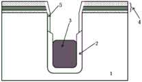
步骤二,如图3所示,在沟槽的上半部淀积形成保护介质层;优选的是采用APCVD法进行淀积,所述形成的保护介质层附着于沟槽上部包括硬掩模层的侧壁及沟槽内下部的多晶硅上表面。形成保护介质层厚度为

淀积完成之后还进行一些热退火步骤。Some thermal annealing steps are also performed after the deposition is complete.
步骤三,如图4所示,在沟槽内整体淀积一层多晶硅层间氧化层;淀积的多晶硅层间氧化层填充满沟槽并在半导体基板表面整体淀积,将ONO硬掩模层也整体覆盖住。
步骤四,如图5所示,对淀积的多晶硅层间氧化层进行CMP工艺;从淀积的膜表面向下研磨,以硬掩模层中的氮化层为研磨终止点,研磨至ONO层中的氮化层表面。
步骤五,继续对多晶硅层间氧化层进行湿法刻蚀工艺,对硬掩模中剩余的氮化硅层及氧化层,以及淀积的多晶硅层间氧化层进行刻蚀,包括去除沟槽侧壁的保护介质层,如图6所示;使沟槽内剩余的多晶硅层间氧化层达到设计厚度,成为上部多晶硅与下部多晶硅之间的隔离介质层。Step 5: Continue to perform wet etching process on the polysilicon interlayer oxide layer, etch the remaining silicon nitride layer and oxide layer in the hard mask, and the deposited polysilicon interlayer oxide layer, including removing the trench side The protective dielectric layer of the wall is shown in Figure 6; the remaining polysilicon interlayer oxide layer in the trench reaches the designed thickness, and becomes the isolation dielectric layer between the upper polysilicon and the lower polysilicon.
本发明上述工艺在多晶硅层间氧化层淀积之前,先在沟槽内壁形成一层保护氧化层,放置后续的多晶硅层间氧化层淀积工艺导致沟槽顶部拐角圆化,由于圆化的拐角会导致源区注入时,注入结深过深从而引发短沟道效应。本发明淀积保护层对沟槽侧壁进行保护,保证了沟槽顶部形貌不受影响,从而得到近乎直角的沟槽顶部,提高了器件的性能。The above-mentioned process of the present invention first forms a protective oxide layer on the inner wall of the trench before the deposition of the polysilicon interlayer oxide layer, and the subsequent polysilicon interlayer oxide layer deposition process causes the top corner of the trench to be rounded. When the source region is implanted, the implanted junction is too deep to cause a short channel effect. In the present invention, the protective layer is deposited to protect the sidewall of the trench, ensuring that the top shape of the trench is not affected, thereby obtaining a trench top with a nearly right angle, and improving the performance of the device.
如图7所示,是采用本发明工艺后形成的沟槽的剖面显微图,图中虚线框内的显示沟槽顶部拐角接近90°直角,与图1相比顶部形貌得到明显改善。As shown in FIG. 7 , it is a cross-sectional micrograph of the trench formed by the process of the present invention. The top corner of the trench in the dotted frame is close to a right angle of 90°, and the top shape is significantly improved compared with FIG. 1 .
在本发明所述的工艺之后,还包括后续传统的工艺步骤,即在沟槽内淀积第二层多晶硅并回刻,以形成沟槽上部电极,然后进行离子注入形成源区等工艺,是为公知技术,在此不再赘述。After the process of the present invention, it also includes the following traditional process steps, that is, depositing a second layer of polysilicon in the trench and etching back to form the upper electrode of the trench, and then performing ion implantation to form the source region and other processes. It is a well-known technology and will not be repeated here.
以上仅为本发明的优选实施例,并不用于限定本发明。对于本领域的技术人员来说,本发明可以有各种更改和变化。凡在本发明的精神和原则之内,所作的任何修改、等同替换、改进等,均应包含在本发明的保护范围之内。The above are only preferred embodiments of the present invention, and are not intended to limit the present invention. Various modifications and variations of the present invention are possible for those skilled in the art. Any modification, equivalent replacement, improvement, etc. made within the spirit and principle of the present invention shall be included within the protection scope of the present invention.
Claims (8)
Translated fromChinese
Priority Applications (1)
| Application Number | Priority Date | Filing Date | Title |
|---|---|---|---|
| CN202010608772.9ACN111785619A (en) | 2020-06-30 | 2020-06-30 | Process method for shielding trench of gate trench type MOSFET |
Applications Claiming Priority (1)
| Application Number | Priority Date | Filing Date | Title |
|---|---|---|---|
| CN202010608772.9ACN111785619A (en) | 2020-06-30 | 2020-06-30 | Process method for shielding trench of gate trench type MOSFET |
Publications (1)
| Publication Number | Publication Date |
|---|---|
| CN111785619Atrue CN111785619A (en) | 2020-10-16 |
Family
ID=72760164
Family Applications (1)
| Application Number | Title | Priority Date | Filing Date |
|---|---|---|---|
| CN202010608772.9APendingCN111785619A (en) | 2020-06-30 | 2020-06-30 | Process method for shielding trench of gate trench type MOSFET |
Country Status (1)
| Country | Link |
|---|---|
| CN (1) | CN111785619A (en) |
Cited By (4)
| Publication number | Priority date | Publication date | Assignee | Title |
|---|---|---|---|---|
| CN112750696A (en)* | 2020-12-31 | 2021-05-04 | 广州粤芯半导体技术有限公司 | Preparation method of groove type power device |
| CN113725078A (en)* | 2021-09-11 | 2021-11-30 | 捷捷微电(上海)科技有限公司 | Manufacturing method of split gate MOSFET |
| CN115985954A (en)* | 2023-01-04 | 2023-04-18 | 深圳吉华微特电子有限公司 | Manufacturing method for improving polycrystalline morphology of SGT product |
| CN117393501A (en)* | 2023-12-07 | 2024-01-12 | 合肥晶合集成电路股份有限公司 | Semiconductor structure and manufacturing method thereof |
Citations (4)
| Publication number | Priority date | Publication date | Assignee | Title |
|---|---|---|---|---|
| US20120235229A1 (en)* | 2011-03-16 | 2012-09-20 | Probst Dean E | Inter-poly dielectric in a shielded gate mosfet device |
| CN104022043A (en)* | 2014-06-16 | 2014-09-03 | 中航(重庆)微电子有限公司 | Groove type power MOSFET with split gates and manufacturing method |
| CN105448741A (en)* | 2015-12-31 | 2016-03-30 | 上海华虹宏力半导体制造有限公司 | Shield grid groove type MOSFET process method |
| CN108735605A (en)* | 2018-01-23 | 2018-11-02 | 西安龙腾新能源科技发展有限公司 | Improve the shield grid groove MOSFET manufacturing method of channel bottom field plate pattern |
- 2020
- 2020-06-30CNCN202010608772.9Apatent/CN111785619A/enactivePending
Patent Citations (4)
| Publication number | Priority date | Publication date | Assignee | Title |
|---|---|---|---|---|
| US20120235229A1 (en)* | 2011-03-16 | 2012-09-20 | Probst Dean E | Inter-poly dielectric in a shielded gate mosfet device |
| CN104022043A (en)* | 2014-06-16 | 2014-09-03 | 中航(重庆)微电子有限公司 | Groove type power MOSFET with split gates and manufacturing method |
| CN105448741A (en)* | 2015-12-31 | 2016-03-30 | 上海华虹宏力半导体制造有限公司 | Shield grid groove type MOSFET process method |
| CN108735605A (en)* | 2018-01-23 | 2018-11-02 | 西安龙腾新能源科技发展有限公司 | Improve the shield grid groove MOSFET manufacturing method of channel bottom field plate pattern |
Cited By (5)
| Publication number | Priority date | Publication date | Assignee | Title |
|---|---|---|---|---|
| CN112750696A (en)* | 2020-12-31 | 2021-05-04 | 广州粤芯半导体技术有限公司 | Preparation method of groove type power device |
| CN113725078A (en)* | 2021-09-11 | 2021-11-30 | 捷捷微电(上海)科技有限公司 | Manufacturing method of split gate MOSFET |
| CN115985954A (en)* | 2023-01-04 | 2023-04-18 | 深圳吉华微特电子有限公司 | Manufacturing method for improving polycrystalline morphology of SGT product |
| CN117393501A (en)* | 2023-12-07 | 2024-01-12 | 合肥晶合集成电路股份有限公司 | Semiconductor structure and manufacturing method thereof |
| CN117393501B (en)* | 2023-12-07 | 2024-03-19 | 合肥晶合集成电路股份有限公司 | Semiconductor structure and manufacturing method thereof |
Similar Documents
| Publication | Publication Date | Title |
|---|---|---|
| TWI538063B (en) | Double oxide trench gate power MOSFET filled with trenches using oxide | |
| CN111883592B (en) | Shielded gate trench power device and manufacturing method thereof | |
| CN111785619A (en) | Process method for shielding trench of gate trench type MOSFET | |
| US9899477B2 (en) | Edge termination structure having a termination charge region below a recessed field oxide region | |
| CN104485286B (en) | MOSFET comprising middle pressure SGT structures and preparation method thereof | |
| CN109979823B (en) | Shielding gate power device and manufacturing method thereof | |
| CN105514022B (en) | The method that portion surface forms field silica in the trench | |
| CN112509979B (en) | Semiconductor device having a shielded gate trench structure and method of fabricating the same | |
| CN112242305A (en) | Semiconductor device and method for manufacturing the same | |
| CN106298945A (en) | Shield grid trench MOSFET process | |
| CN105428241A (en) | Manufacturing method of trench gate power device with shield grid | |
| CN114284149A (en) | A kind of preparation method of shielded gate trench field effect transistor | |
| US8759910B2 (en) | Trench MOSFET with trenched floating gates having thick trench bottom oxide as termination | |
| CN111128706B (en) | Method for manufacturing field oxygen with graded thickness in trench and method for manufacturing SGT device | |
| KR100487657B1 (en) | mos transistor with recessed gate and method of fabricating the same | |
| TW202137570A (en) | Semiconductor device and manufacturing method thereof | |
| KR20060030717A (en) | Manufacturing Method of Semiconductor Device | |
| CN105655385B (en) | The manufacturing method of groove-shaped super-junction device | |
| CN112038225A (en) | Method for forming gate oxide | |
| CN112864019A (en) | Method for manufacturing semiconductor power device and semiconductor power device | |
| CN110970435A (en) | Semiconductor device and method of forming the same | |
| CN210926025U (en) | Trench gate MOS structure with thick oxide layer at bottom | |
| CN111128703B (en) | Process method of SGT device | |
| CN113410291A (en) | Manufacturing method of shielded gate trench power device | |
| KR100275484B1 (en) | Method for manufacturing a power device having a trench gate electrode |
Legal Events
| Date | Code | Title | Description |
|---|---|---|---|
| PB01 | Publication | ||
| PB01 | Publication | ||
| SE01 | Entry into force of request for substantive examination | ||
| SE01 | Entry into force of request for substantive examination | ||
| RJ01 | Rejection of invention patent application after publication | Application publication date:20201016 | |
| RJ01 | Rejection of invention patent application after publication |