CN111785169A - A display device and method of making the same - Google Patents
A display device and method of making the sameDownload PDFInfo
- Publication number
- CN111785169A CN111785169ACN202010680271.1ACN202010680271ACN111785169ACN 111785169 ACN111785169 ACN 111785169ACN 202010680271 ACN202010680271 ACN 202010680271ACN 111785169 ACN111785169 ACN 111785169A
- Authority
- CN
- China
- Prior art keywords
- flat plate
- display device
- support film
- bending
- fixing
- Prior art date
- Legal status (The legal status is an assumption and is not a legal conclusion. Google has not performed a legal analysis and makes no representation as to the accuracy of the status listed.)
- Pending
Links
Images


Classifications
- G—PHYSICS
- G09—EDUCATION; CRYPTOGRAPHY; DISPLAY; ADVERTISING; SEALS
- G09F—DISPLAYING; ADVERTISING; SIGNS; LABELS OR NAME-PLATES; SEALS
- G09F9/00—Indicating arrangements for variable information in which the information is built-up on a support by selection or combination of individual elements
- G09F9/30—Indicating arrangements for variable information in which the information is built-up on a support by selection or combination of individual elements in which the desired character or characters are formed by combining individual elements
- G09F9/301—Indicating arrangements for variable information in which the information is built-up on a support by selection or combination of individual elements in which the desired character or characters are formed by combining individual elements flexible foldable or roll-able electronic displays, e.g. thin LCD, OLED
Landscapes
- Physics & Mathematics (AREA)
- General Physics & Mathematics (AREA)
- Engineering & Computer Science (AREA)
- Theoretical Computer Science (AREA)
- Devices For Indicating Variable Information By Combining Individual Elements (AREA)
Abstract
Description
Translated fromChinese技术领域technical field
本发明涉及显示技术领域,特别涉及一种显示装置及制作方法。The present invention relates to the field of display technology, and in particular, to a display device and a manufacturing method.
背景技术Background technique
为了实现柔性显示装置的窄边框设计,往往将连接柔性电路板(FlexibleCircuit Board,FPC)和驱动芯片(Integrated Circuit,IC)的基材部分弯折至显示面板的背面。然而,弯折过程所产生的较大回弹力会导致显示装置的部分膜层出现变形甚至崩开的问题,从而降低显示装置的良率。In order to realize the narrow frame design of the flexible display device, the part of the base material connecting the flexible circuit board (FPC) and the driving chip (Integrated Circuit, IC) is often bent to the back of the display panel. However, the large elastic force generated by the bending process may cause deformation or even collapse of some of the film layers of the display device, thereby reducing the yield of the display device.
发明内容SUMMARY OF THE INVENTION
本发明提供了一种显示装置及制作方法,用于降低显示装置中部分膜层发生变形甚至崩开的风险,提高显示装置的良率。The present invention provides a display device and a manufacturing method, which are used to reduce the risk of deformation or even collapse of some film layers in the display device, and improve the yield of the display device.
第一方面,本发明实施例提供了一种显示装置,包括:In a first aspect, an embodiment of the present invention provides a display device, including:
显示面板,所述显示面板包括平板部、弯折部和固定部,其中,所述弯折部位于所述平板部和所述固定部之间,所述固定部通过所述弯折部弯折至所述平板部的背面;A display panel, the display panel includes a flat plate part, a bending part and a fixing part, wherein the bending part is located between the flat plate part and the fixing part, and the fixing part is bent by the bending part to the back of the flat plate portion;
设置在所述平板部背面的第一支撑膜,设置在所述固定部面向所述平板部一侧的第二支撑膜;a first support film disposed on the back of the flat plate portion, and a second support film disposed on the side of the fixing portion facing the flat plate portion;
设置在所述弯折部内侧的固定胶,且所述固定胶位于所述第一支撑膜和所述第二支撑膜之间。The fixing glue is arranged on the inner side of the bending part, and the fixing glue is located between the first support film and the second support film.
在一种可能的实现方式中,所述固定胶的弹性模量范围为20Mpa~100Mpa。In a possible implementation manner, the elastic modulus of the fixing glue ranges from 20Mpa to 100Mpa.
在一种可能的实现方式中,所述固定胶包括靠近所述第一支撑膜的第一端,和靠近所述第二支撑膜的第二端,所述第一端与所述第二端贴合接触。In a possible implementation, the fixing glue includes a first end close to the first support film and a second end close to the second support film, the first end and the second end Fit contact.
在一种可能的实现方式中,所述固定胶填充所述弯折部所形成的凹槽区域的至少部分区域。In a possible implementation manner, the fixing glue fills at least a part of the groove region formed by the bending portion.
在一种可能的实现方式中,沿靠近所述弯折轴的方向,所述固定胶沿垂直于所述平板部所在平面方向的厚度逐渐减小。In a possible implementation manner, along a direction close to the bending axis, the thickness of the fixing glue gradually decreases along a direction perpendicular to the plane where the flat plate portion is located.
在一种可能的实现方式中,沿靠近所述弯折轴的方向,所述固定胶沿平行于所述平板部所在平面方向的厚度逐渐增大。In a possible implementation manner, along a direction close to the bending axis, the thickness of the fixing glue gradually increases along a direction parallel to the plane where the flat plate portion is located.
在一种可能的实现方式中,所述弯折部外侧设置有保护胶层。In a possible implementation manner, a protective adhesive layer is provided on the outer side of the bending portion.
在一种可能的实现方式中,所述第一支撑膜背离所述平板部的一侧依次设置有胶材层、缓冲层、散热层。In a possible implementation manner, an adhesive material layer, a buffer layer, and a heat dissipation layer are sequentially provided on the side of the first support film facing away from the flat plate portion.
第二方面,本发明实施例提供了一种如上面所述的显示装置的制作方法,包括:In a second aspect, an embodiment of the present invention provides a method for manufacturing a display device as described above, including:
将所述第一支撑膜设置在所述平板部的背面,以及将所述第二支撑膜设置在所述固定部的背面;disposing the first support film on the backside of the flat plate portion, and disposing the second support film on the backside of the fixing portion;
将所述固定胶涂覆在所述弯折部位于所述第一支撑膜和所述第二支撑膜之间的区域内;coating the fixing glue in the area of the bent portion between the first support film and the second support film;
通过所述弯折部将所述固定部弯折至所述平板部的背面。The fixing portion is bent to the back surface of the flat plate portion by the bending portion.
第三方面,本发明实施例提供了一种如上面所述的显示装置的制作方法,包括:In a third aspect, an embodiment of the present invention provides a method for fabricating a display device as described above, including:
将所述第一支撑膜设置在所述平板部的背面,以及将所述第二支撑膜设置在所述固定部的背面;disposing the first support film on the backside of the flat plate portion, and disposing the second support film on the backside of the fixing portion;
通过所述弯折部将所述固定部弯折至所述平板部的背面;Bending the fixing part to the back of the flat plate part through the bending part;
将所述固定胶填充至所述弯折部所形成的凹槽区域的至少部分区域内。Filling the fixing glue into at least part of the groove area formed by the bending portion.
本发明的有益效果如下:The beneficial effects of the present invention are as follows:
本发明实施例提供了一种显示装置及制作方法,其中,该显示装置包括显示面板,显示面板包括平板部、弯折部和固定部,弯折部位于平板部和固定部之间,固定部通过弯折部弯折至平板部的背面,设置在平板部背面的第一支撑膜,设置在固定部面向平板部一侧的第二支撑膜,设置在弯折部内侧的固定胶,且固定胶位于第一支撑膜和第二支撑膜之间,这样的话,设置在第一支撑膜和第二支撑膜之间的固定胶能够有效削弱显示面板的弯折部因弯折所产生的回弹力,从而降低显示装置中部分膜层发生变形甚至崩开的风险,从而提高显示装置的良率。Embodiments of the present invention provide a display device and a manufacturing method, wherein the display device includes a display panel, the display panel includes a flat plate portion, a bending portion and a fixing portion, the bending portion is located between the flat plate portion and the fixing portion, and the fixing portion The bending part is bent to the back of the flat plate part, the first support film is arranged on the back of the flat plate part, the second support film is arranged on the side of the fixing part facing the flat plate part, the fixing glue is arranged on the inner side of the bending part, and is fixed The glue is located between the first support film and the second support film. In this case, the fixing glue disposed between the first support film and the second support film can effectively weaken the resilience of the bending portion of the display panel due to bending. , thereby reducing the risk of deformation or even collapse of some film layers in the display device, thereby improving the yield of the display device.
附图说明Description of drawings
图1为相关技术中触控显示装置的其中一种结构示意图;FIG. 1 is a schematic structural diagram of a touch display device in the related art;
图2为本发明实施例提供的一种显示装置的结构示意图;FIG. 2 is a schematic structural diagram of a display device according to an embodiment of the present invention;
图3为图1中弯折部边缘应力的其中一种分布示意图;FIG. 3 is a schematic diagram of one of the distributions of the edge stress of the bending portion in FIG. 1;
图4为图2中弯折部边缘应力的其中一种分布示意图;FIG. 4 is a schematic diagram of one of the distributions of the edge stress of the bending portion in FIG. 2;
图5为本发明实施例提供的一种显示装置的其中一种结构示意图;FIG. 5 is a schematic structural diagram of one of a display device according to an embodiment of the present invention;
图6为本发明实施例提供的一种显示装置中弯折部未弯折前的其中一种结构示意图;6 is a schematic structural diagram of one of the structures of a display device provided in an embodiment of the present invention before the bending portion is not bent;
图7为本发明实施例提供的一种显示装置的其中一种结构示意图;FIG. 7 is a schematic structural diagram of a display device according to an embodiment of the present invention;
图8为本发明实施例提供的一种显示装置的制作方法的方法流程图;8 is a method flowchart of a method for manufacturing a display device according to an embodiment of the present invention;
图9为本发明实施例提供的一种显示装置的制作方法的方法流程图。FIG. 9 is a method flowchart of a method for fabricating a display device according to an embodiment of the present invention.
具体实施方式Detailed ways
为使本发明实施例的目的、技术方案和优点更加清楚,下面将结合本发明实施例的附图,对本发明实施例的技术方案进行清楚、完整地描述。显然,所描述的实施例是本发明的一部分实施例,而不是全部的实施例。并且在不冲突的情况下,本发明中的实施例及实施例中的特征可以相互组合。基于所描述的本发明的实施例,本领域普通技术人员在无需创造性劳动的前提下所获得的所有其他实施例,都属于本发明保护的范围。In order to make the purpose, technical solutions and advantages of the embodiments of the present invention clearer, the technical solutions of the embodiments of the present invention will be clearly and completely described below with reference to the accompanying drawings of the embodiments of the present invention. Obviously, the described embodiments are some, but not all, embodiments of the present invention. Also, the embodiments of the present invention and the features of the embodiments may be combined with each other without conflict. Based on the described embodiments of the present invention, all other embodiments obtained by those of ordinary skill in the art without creative work fall within the protection scope of the present invention.
除非另外定义,本发明使用的技术术语或者科学术语应当为本发明所属领域内具有一般技能的人士所理解的通常意义。本发明中使用的“包括”或者“包含”等类似的词语意指出现该词前面的元件或者物件涵盖出现在该词后面列举的元件或者物件及其等同,而不排除其他元件或者物件。Unless otherwise defined, technical or scientific terms used in the present invention should have the ordinary meaning as understood by one of ordinary skill in the art to which the present invention belongs. When used herein, "comprises" or "comprising" and similar words mean that the elements or things appearing before the word encompass the elements or things listed after the word and their equivalents, but do not exclude other elements or things.
需要注意的是,附图中各图形的尺寸和形状不反映真实比例,目的只是示意说明本发明内容。并且自始至终相同或类似的标号表示相同或类似的元件或具有相同或类似功能的元件。It should be noted that the dimensions and shapes of the figures in the accompanying drawings do not reflect the actual scale, and are only intended to illustrate the content of the present invention. And the same or similar reference numerals refer to the same or similar elements or elements having the same or similar functions throughout.
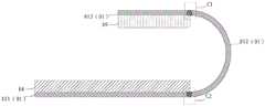
目前,在显示装置内设置各种模组结构,以此来提高显示装置的使用性能,比如,可以起到器件缓冲保护及散热的模组结构。比如,如图1所示的触控显示装置,该触控显示装置在可操作区(Active Area,AA)的显示面板01和触控面板02通过黏胶层贴合在一起,触控面板02远离显示面板01的一侧设置有盖板03;其中,显示面板01包括平板部011、弯折部012和固定部013,弯折部012位于平板部011和固定部013之间,固定部013通过弯折部012弯折至平板部011的背面;该触控显示装置还包括位于平板部011与固定部013之间依次层叠设置的第一背膜04、第一胶层05、缓冲层06、散热层07、第二胶层08、第二背膜09,固定部背离平板部的一侧还设置有FPC 00,在显示面板01的弯折部012进行弯折时,弯折过程中产生的较大回弹力F将作用在缓冲层06,使得缓冲层06靠近弯折部012的一侧产生变形甚至崩开,从而影响触控显示装置的良率。At present, various module structures are provided in the display device to improve the usability of the display device, for example, the module structure can play the role of device buffer protection and heat dissipation. For example, in the touch display device shown in FIG. 1 , the
鉴于此,本发明实施例提供了一种显示装置及制作方法,用于降低显示装置中部分膜层发生变形甚至崩开的风险,提高显示装置的良率。In view of this, embodiments of the present invention provide a display device and a manufacturing method, which are used to reduce the risk of deformation or even collapse of some film layers in the display device, and improve the yield of the display device.
如图2所示为本发明实施例提供的一种显示装置的结构示意图,具体来讲,该显示装置包括:FIG. 2 is a schematic structural diagram of a display device according to an embodiment of the present invention. Specifically, the display device includes:
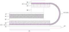
显示面板10,显示面板10包括平板部101、弯折部102和固定部103,其中,弯折部102位于平板部101和固定部103之间,固定部103通过弯折部102弯折至平板部101的背面;The
在具体实施过程中,平板部101用于画面显示,固定部103用于绑定驱动芯片。In the specific implementation process, the
设置在平板部101背面的第一支撑膜20,设置在固定部103面向平板部101一侧的第二支撑膜30;The
在具体实施过程中,第一支撑膜20和第二支撑膜30均包括基底及涂布在该基底上胶材,其中,基底通常为高分子材料,通过第一支撑膜20和第二支撑膜30对显示面板10进行了有效的支撑保护,避免了在显示装置的后续工艺中对显示面板10的损伤。在具体实施过程中,第一支撑膜20和第二支撑膜30中可以是同种基底和胶材所制成的背膜,还可以是不同胶材所制成的背膜,在此不做限定。In a specific implementation process, both the
设置在所述弯折部102内侧的固定胶40,且所述固定胶40位于所述第一支撑膜20和所述第二支撑膜30之间。The
在具体实施过程中,设置在弯折部102内侧的固定胶40,还位于第一支撑膜20和第二支撑膜30之间,不仅保证了平板部101与弯折部102间的平缓过渡,还保证了弯折部102与固定部103间的平缓过渡,从而对来自弯折部102的应力进行有效的分散,避免了显示面板10的弯折部102因应力集中所致的走线断裂,保证了显示装置的良率。本发明人在实际研究中发现在设置固定胶40前后,弯折部102的边缘应力分布的示意图分别如图3和图4所示,其中,图3为图1中弯折部012内侧未设置固定胶时其边缘应力的其中一种分布示意图,图3中虚线框区域C1和C2为应力分布区域。图4为图2中弯折部102内侧设置固定胶40时其边缘应力的其中一种分布示意图,图4中虚线框区域D1和D2为应力分布区域。图4相较于图3而言,应力分布更为分散,相应地对显示面板10的作用力更小,从而避免了弯折部102边缘因应力集中所致的走线断裂。In the specific implementation process, the
在具体实施过程中,由于设置在弯折部102内侧的固定胶40,还会对弯折部102施加与回弹力方向相反的粘结力,从而削弱了显示面板10的弯折部102因弯折所产生的回弹力,进而降低显示装置中部分膜层发生变形甚至崩开的风险,提高了显示装置的良率。In the specific implementation process, due to the fixing
在本发明实施例中,固定胶40的弹性模量范围为20Mpa~100Mpa,比如,固定胶40的弹性模量为41Mpa。在具体实施过程中,选择较高弹性模量的固定胶40,相应地,固定胶40越柔软,对弯折部102弯折所产生的回弹力的削弱效果越好,从而降低了显示装置中部分膜层发生变形甚至崩开的风险。In the embodiment of the present invention, the elastic modulus of the fixing
在本发明实施例中,固定胶40包括聚碳酸酯、聚丙烯酸中的至少一种。在具体实施过程中,本领域技术人员可以根据实际应用中对弯折部102所产生回弹力的削弱效果来选择相应材料的固定胶40,在此不做限定。In the embodiment of the present invention, the fixing
在本发明实施例中,如图5所示为显示装置的其中一种结构示意图,具体来讲,固定胶40包括靠近第一支撑膜20的第一端401,和靠近第二支撑膜30的第二端402,第一端401与第二端402贴合接触。如图6所示为显示装置中的弯折部102未弯折前的其中一种结构示意图。图5为图6中弯折部102弯折后的结构示意图。在具体实施过程中,由于在弯折部102弯折后,固定胶40的第一端401和第二端402贴合接触,此时,由于固定胶40的第一端401和第二端402贴合接触从而产生了与回弹力方向相反的力F’。如图5所示为固定部103与弯折部102相接的位置为受力点,弯折部102因弯折所产生的回弹力为F,因固定胶40两端贴合接触所产生的力F’,与回弹力F方向相反,从而削弱了回弹力F对显示装置可操作区AA内的膜层的应力作用,降低了显示装置中部分膜层发生变形甚至崩开的风险。In the embodiment of the present invention, FIG. 5 is a schematic diagram of one of the structures of the display device. Specifically, the fixing
在具体实施过程中,固定胶40的第一端401可以与第一支撑膜20接触,如图2所示,还可以是与第一支撑膜20间隔第一预设距离,如图5所示,其中,该第一预设距离可以是实际工艺误差所导致的距离,还可以是根据实际应用需要所设定的距离,在此不做限定。固定胶40的第二端402可以与第二支撑膜30接触,还可以是与第二支撑膜30间隔第二预设距离,该第二预设距离可以是实际工艺误差所导致的距离,还可以是根据实际应用需要所设定的距离,在此不做限定。In a specific implementation process, the
在本发明实施例中,固定胶40填充弯折部102所形成的凹槽区域的至少部分区域。在具体实施过程中,固定胶40可以是完全填满弯折部102所形成的凹槽区域,如图2所示,还可以是仅填充凹槽区域的部分区域,如图5所示。在实际应用中可以根据对回弹力的削弱需求来填充固定胶40,在此不做限定。In the embodiment of the present invention, the fixing
在本发明实施例中,沿靠近弯折轴的方向,固定胶40沿垂直于平板部101所在平面方向的厚度逐渐减小。结合图2所示的显示装置,离弯折轴越远,固定胶40沿垂直于平板部101所在平面方向的厚度越大,相应地,对弯折部102与固定部103紧邻位置处的回弹力的削弱效果越好,降低了对显示装置中可操作区AA内的相关膜层的损伤。此外,固定胶40在不同位置的不同厚度对弯折部102相应位置的应力进行相应的削弱,从而降低了设置在弯折部102的电路走线的断线风险,进而提高了显示装置的良率。In the embodiment of the present invention, along the direction close to the bending axis, the thickness of the fixing
在本发明实施例中,沿靠近弯折轴的方向,固定胶40沿平行于平板部101所在平面方向的厚度逐渐增大。结合图2所示的显示装置,离弯折轴越近,固定胶40沿平行于平板部101所在平面方向的厚度越大,相应地,对弯折部102曲率最大处的应力的削弱效果越好,降低了设置在弯折部102的电路走线的断线风险。In the embodiment of the present invention, along the direction close to the bending axis, the thickness of the fixing
在本发明实施例中,弯折部102外侧设置有保护胶层,该保护胶层可以是MCL胶层,这样的话,能够有效防止弯折部102弯折过程中对电路走线的损伤,进而提高显示装置的良率。In the embodiment of the present invention, the outer side of the bending
如图7所示为本发明实施例提供的一种显示装置的其中一种结构示意图,具体来讲,第一支撑膜20背离平板部101的一侧依次设置有胶材层50、缓冲层60、散热层70。在具体实施例中,通过固定胶40削弱显示面板10的弯折部102因弯折所产生的回弹力,能够降低缓冲层60变形,甚至从胶材层50上崩开的风险,从而保证了缓冲层60对显示面板10的缓冲保护,以及散热层70对显示装置的散热效果,进而提高了显示装置的良率。FIG. 7 is a schematic structural diagram of a display device according to an embodiment of the present invention. Specifically, the side of the
在具体实施过程中,胶材层50可以是网格胶(Embossing,EMBO)。缓冲层60可以为泡棉,能够对显示装置中所设置的元器件或面板进行缓冲保护。散热层70可以由金、银、铜等至少一种金属材料制备而成,还可以由石墨烯等非金属材料制备而成,此外,还可以选择其它导热性能较好的材料来制备散热层70,当然,本领域技术人员可以根据实际需要来选择相应材料来制备散热层70,在此不做限定。In a specific implementation process, the
此外,在具体实施过程中,对于显示装置中的其它膜层同现有技术中的相关设计,在此就不再详述赘述。In addition, in the specific implementation process, the other film layers in the display device and the related designs in the prior art will not be described in detail here.
基于同样的发明构思,如图8所示,本发明实施例还提供了一种显示装置的制作方法,包括:Based on the same inventive concept, as shown in FIG. 8 , an embodiment of the present invention also provides a method for manufacturing a display device, including:
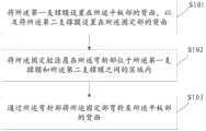
S101:将所述第一支撑膜设置在所述平板部的背面,以及将所述第二支撑膜设置在所述固定部的背面;S101: disposing the first support film on the backside of the flat plate portion, and disposing the second support film on the backside of the fixing portion;
S102:将所述固定胶涂覆在所述弯折部位于所述第一支撑膜和所述第二支撑膜之间的区域内;S102: Coating the fixing glue in the area of the bent portion between the first support film and the second support film;
S103:通过所述弯折部将所述固定部弯折至所述平板部的背面。S103: Bending the fixing portion to the back of the flat plate portion through the bending portion.
在具体实施过程中,步骤S101至步骤S103的具体实现过程如下:In the specific implementation process, the specific implementation process of step S101 to step S103 is as follows:
首先,在弯折部弯折前,将第一支撑膜设置在平板部的背面,并将第二支撑膜设置在固定部的背面,具体可以是剥离掉贴附在第一支撑膜相对两侧的离型膜,将第一支撑膜设置在平板部的背面,同理,剥离掉贴附在第二支撑膜相对两侧的离型膜,将第二支撑膜设置在固定部的背面。然后,将固定胶涂覆在弯折部位于第一支撑膜和第二支撑膜之间的区域内,然后,通过弯折部将固定部弯折至平板部的背面。在具体实施过程中,由于在弯折部弯折前,就将固定胶涂覆在弯折部位于第一支撑膜和第二支撑膜之间的区域内,这样的话,在弯折过程中,通过固定胶一方面对弯折部与固定部边缘位置处的应力进行了分散,另一方面,有效削弱了弯折部弯折过程中所产生的回弹力,从而提高了显示装置的良率。基于同样的发明构思,如图9所示,本发明实施例还提供了一种显示装置的制作方法,包括:First, before the bending part is bent, the first support film is set on the back of the flat plate part, and the second support film is set on the back of the fixed part, specifically, it can be peeled off and attached to the opposite sides of the first support film For the release film, set the first support film on the back of the flat plate part. Similarly, peel off the release film attached to the opposite sides of the second support film, and set the second support film on the back of the fixed part. Then, the fixing glue is applied in the area of the bending part between the first supporting film and the second supporting film, and then the fixing part is bent to the back of the flat plate part through the bending part. In the specific implementation process, before the bending part is bent, the fixing glue is applied to the area of the bending part between the first support film and the second support film, so that during the bending process, On the one hand, the fixing glue disperses the stress at the edge of the bending portion and the fixing portion, and on the other hand, effectively weakens the resilience generated during the bending process of the bending portion, thereby improving the yield of the display device. Based on the same inventive concept, as shown in FIG. 9 , an embodiment of the present invention also provides a manufacturing method of a display device, including:
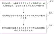
S201:将所述第一支撑膜设置在所述平板部的背面,以及将所述第二支撑膜设置在所述固定部的背面;S201: disposing the first support film on the back of the flat plate portion, and disposing the second support film on the back of the fixing portion;
S202:通过所述弯折部将所述固定部弯折至所述平板部的背面;S202: Bending the fixing portion to the back of the flat plate portion through the bending portion;
S203:将所述固定胶填充至所述弯折部所形成的凹槽区域的至少部分区域内。S203: Fill the fixing glue into at least a part of the groove area formed by the bending portion.
在具体实施过程中,步骤S201至步骤S203的具体实现过程如下:In the specific implementation process, the specific implementation process of step S201 to step S203 is as follows:
首先,在弯折部弯折前,将第一支撑膜设置在平板部的背面,并将第二支撑膜设置在固定部的背面,具体可以是剥离掉贴附在第一支撑膜相对两侧的离型膜,将第一支撑膜设置在平板部的背面,同理,剥离掉贴附在第二支撑膜相对两侧的离型膜,将第二支撑膜设置在固定部的背面。然后,通过弯折部将固定部弯折至平板部的背面,然后,将固定胶填充至弯折部所形成的凹槽区域的至少部分区域内。在具体实施过程中,通过弯折部将固定部弯折至平板部的背面之后,可以通过注塑的方式,将固定胶填充至弯折部所形成的凹槽区域的至少部分区域内。在填充固定胶之后,通过固定胶对弯折部弯折所产生的回弹力在一定程度上进行了削弱,从而降低了显示装置中部分膜层发生变形甚至崩开的风险,提高了良率。First, before the bending part is bent, the first support film is set on the back of the flat plate part, and the second support film is set on the back of the fixed part, specifically, it can be peeled off and attached to the opposite sides of the first support film For the release film, set the first support film on the back of the flat plate part. Similarly, peel off the release film attached to the opposite sides of the second support film, and set the second support film on the back of the fixed part. Then, the fixing part is bent to the back of the flat plate part through the bending part, and then, the fixing glue is filled into at least part of the groove area formed by the bending part. In a specific implementation process, after the fixing part is bent to the back of the flat plate part by the bending part, the fixing glue can be filled into at least part of the groove area formed by the bending part by means of injection molding. After the fixing glue is filled, the resilient force generated by the bending of the bending part is weakened to a certain extent by the fixing glue, thereby reducing the risk of deformation or even collapse of some film layers in the display device, and improving the yield.
在本发明实施例中,除了图8中步骤S101和图9中步骤201所示方式来设置第一支撑膜和第二支撑膜之外,可以将一整层支撑膜设置在显示面板的背面,然后,采用诸如激光切割方式,去除位于显示面板的弯折部背面的部分支撑膜,形成间隔一定距离设置的第一支撑膜和第二支撑膜,这样的话,所述第一支撑膜位于所述平板部的背面,所述第二支撑膜位于所述固定部的背面,当然,本领域技术人员可以根据实际需要来采用相应的制作工艺来设置第一支撑膜和第二支撑,在此不再详述。In the embodiment of the present invention, in addition to disposing the first support film and the second support film as shown in step S101 in FIG. 8 and step 201 in FIG. 9 , a whole layer of support film may be disposed on the back of the display panel, Then, using a method such as laser cutting, remove part of the supporting film located on the back of the bent portion of the display panel to form a first supporting film and a second supporting film arranged at a certain distance. In this case, the first supporting film is located in the The backside of the flat plate portion, the second support film is located on the backside of the fixed portion, of course, those skilled in the art can use the corresponding manufacturing process to set the first support film and the second support according to actual needs, and will not be repeated here. detail.
尽管已描述了本发明的优选实施例,但本领域内的技术人员一旦得知了基本创造性概念,则可对这些实施例作出另外的变更和修改。所以,所附权利要求意欲解释为包括优选实施例以及落入本发明范围的所有变更和修改。Although preferred embodiments of the present invention have been described, additional changes and modifications to these embodiments may occur to those skilled in the art once the basic inventive concepts are known. Therefore, the appended claims are intended to be construed to include the preferred embodiment and all changes and modifications that fall within the scope of the present invention.
显然,本领域的技术人员可以对本申请进行各种改动和变型而不脱离本申请的精神和范围。这样,倘若本申请的这些修改和变型属于本申请权利要求及其等同技术的范围之内,则本申请也意图包含这些改动和变型在内。Obviously, those skilled in the art can make various changes and modifications to the present application without departing from the spirit and scope of the present application. Thus, if these modifications and variations of the present application fall within the scope of the claims of the present application and their equivalents, the present application is also intended to include these modifications and variations.
Claims (10)
Priority Applications (1)
| Application Number | Priority Date | Filing Date | Title |
|---|---|---|---|
| CN202010680271.1ACN111785169A (en) | 2020-07-15 | 2020-07-15 | A display device and method of making the same |
Applications Claiming Priority (1)
| Application Number | Priority Date | Filing Date | Title |
|---|---|---|---|
| CN202010680271.1ACN111785169A (en) | 2020-07-15 | 2020-07-15 | A display device and method of making the same |
Publications (1)
| Publication Number | Publication Date |
|---|---|
| CN111785169Atrue CN111785169A (en) | 2020-10-16 |
Family
ID=72768726
Family Applications (1)
| Application Number | Title | Priority Date | Filing Date |
|---|---|---|---|
| CN202010680271.1APendingCN111785169A (en) | 2020-07-15 | 2020-07-15 | A display device and method of making the same |
Country Status (1)
| Country | Link |
|---|---|
| CN (1) | CN111785169A (en) |
Cited By (5)
| Publication number | Priority date | Publication date | Assignee | Title |
|---|---|---|---|---|
| CN113470529A (en)* | 2021-06-30 | 2021-10-01 | 云谷(固安)科技有限公司 | Display device |
| CN114038315A (en)* | 2021-10-29 | 2022-02-11 | 昆山工研院新型平板显示技术中心有限公司 | Display panel and display device |
| CN114694506A (en)* | 2022-03-18 | 2022-07-01 | 武汉华星光电半导体显示技术有限公司 | Display device |
| CN115171527A (en)* | 2022-06-20 | 2022-10-11 | 昆山国显光电有限公司 | Display panel manufacturing method and display panel |
| WO2023226961A1 (en)* | 2022-05-23 | 2023-11-30 | 京东方科技集团股份有限公司 | Heat dissipation structure, display module, electronic device and processing method for display module |
Citations (7)
| Publication number | Priority date | Publication date | Assignee | Title |
|---|---|---|---|---|
| CN105523281A (en)* | 2016-01-04 | 2016-04-27 | 京东方科技集团股份有限公司 | Flexible supporting structure and display device comprising flexible supporting structure |
| CN105702170A (en)* | 2016-04-05 | 2016-06-22 | 京东方科技集团股份有限公司 | Adhesive material, flexible module, display equipment and manufacturing method of flexible module |
| CN105870355A (en)* | 2016-05-27 | 2016-08-17 | 京东方科技集团股份有限公司 | Flexible OLED device and preparation method thereof |
| CN107094194A (en)* | 2017-05-09 | 2017-08-25 | 京东方科技集团股份有限公司 | A kind of mobile terminal and its falling protection method |
| CN108281387A (en)* | 2018-01-23 | 2018-07-13 | 武汉华星光电半导体显示技术有限公司 | The production method and flexible display apparatus of flexible display apparatus |
| CN109461382A (en)* | 2018-12-03 | 2019-03-12 | 武汉华星光电半导体显示技术有限公司 | Bent panel and preparation method thereof |
| CN210489620U (en)* | 2019-12-02 | 2020-05-08 | 京东方科技集团股份有限公司 | Display substrate and display device |
- 2020
- 2020-07-15CNCN202010680271.1Apatent/CN111785169A/enactivePending
Patent Citations (7)
| Publication number | Priority date | Publication date | Assignee | Title |
|---|---|---|---|---|
| CN105523281A (en)* | 2016-01-04 | 2016-04-27 | 京东方科技集团股份有限公司 | Flexible supporting structure and display device comprising flexible supporting structure |
| CN105702170A (en)* | 2016-04-05 | 2016-06-22 | 京东方科技集团股份有限公司 | Adhesive material, flexible module, display equipment and manufacturing method of flexible module |
| CN105870355A (en)* | 2016-05-27 | 2016-08-17 | 京东方科技集团股份有限公司 | Flexible OLED device and preparation method thereof |
| CN107094194A (en)* | 2017-05-09 | 2017-08-25 | 京东方科技集团股份有限公司 | A kind of mobile terminal and its falling protection method |
| CN108281387A (en)* | 2018-01-23 | 2018-07-13 | 武汉华星光电半导体显示技术有限公司 | The production method and flexible display apparatus of flexible display apparatus |
| CN109461382A (en)* | 2018-12-03 | 2019-03-12 | 武汉华星光电半导体显示技术有限公司 | Bent panel and preparation method thereof |
| CN210489620U (en)* | 2019-12-02 | 2020-05-08 | 京东方科技集团股份有限公司 | Display substrate and display device |
Cited By (8)
| Publication number | Priority date | Publication date | Assignee | Title |
|---|---|---|---|---|
| CN113470529A (en)* | 2021-06-30 | 2021-10-01 | 云谷(固安)科技有限公司 | Display device |
| CN114038315A (en)* | 2021-10-29 | 2022-02-11 | 昆山工研院新型平板显示技术中心有限公司 | Display panel and display device |
| CN114038315B (en)* | 2021-10-29 | 2024-08-30 | 昆山工研院新型平板显示技术中心有限公司 | Display panel and display device |
| CN114694506A (en)* | 2022-03-18 | 2022-07-01 | 武汉华星光电半导体显示技术有限公司 | Display device |
| CN114694506B (en)* | 2022-03-18 | 2023-11-28 | 武汉华星光电半导体显示技术有限公司 | display device |
| WO2023226961A1 (en)* | 2022-05-23 | 2023-11-30 | 京东方科技集团股份有限公司 | Heat dissipation structure, display module, electronic device and processing method for display module |
| CN115171527A (en)* | 2022-06-20 | 2022-10-11 | 昆山国显光电有限公司 | Display panel manufacturing method and display panel |
| CN115171527B (en)* | 2022-06-20 | 2023-10-27 | 昆山国显光电有限公司 | Display panel manufacturing method and display panel |
Similar Documents
| Publication | Publication Date | Title |
|---|---|---|
| CN111785169A (en) | A display device and method of making the same | |
| CN111477670B (en) | a display device | |
| CN113724603B (en) | Display module | |
| WO2022267125A1 (en) | Display module and mobile terminal | |
| CN109994606A (en) | flexible display panel | |
| CN112967604B (en) | Flexible display module and display device | |
| CN111640374A (en) | Display module and display device | |
| WO2022179162A1 (en) | Foldable display device and method for manufacturing same | |
| CN112599018B (en) | Display device | |
| CN110718159A (en) | OLED display screen and OLED display device | |
| CN111696443A (en) | Display device | |
| CN112164314B (en) | Method for manufacturing a display device and display device | |
| CN113629124B (en) | Heat dissipation film and curved surface display device | |
| CN114999327A (en) | Flexible cover plate, display module and display device | |
| WO2023102967A1 (en) | Display panel and display device | |
| TW202103910A (en) | Display | |
| CN113687461B (en) | Polarizing plate, folding module and display device | |
| CN114497085A (en) | Display module and preparation method thereof, and display device | |
| CN117835751A (en) | Display panel and display device | |
| CN116129743A (en) | Display module, manufacturing method thereof, and display device | |
| CN111754874A (en) | display device | |
| CN116072006A (en) | Display assembly and display device | |
| CN115578935A (en) | Display module and mobile terminal | |
| CN112959804B (en) | Curved screen bending device and curved screen bending method | |
| WO2025129952A1 (en) | Display panel and display device |
Legal Events
| Date | Code | Title | Description |
|---|---|---|---|
| PB01 | Publication | ||
| PB01 | Publication | ||
| SE01 | Entry into force of request for substantive examination | ||
| SE01 | Entry into force of request for substantive examination | ||
| RJ01 | Rejection of invention patent application after publication | Application publication date:20201016 | |
| RJ01 | Rejection of invention patent application after publication |