CN111769191A - A kind of ultraviolet LED chip heat dissipation composite substrate - Google Patents
A kind of ultraviolet LED chip heat dissipation composite substrateDownload PDFInfo
- Publication number
- CN111769191A CN111769191ACN202010763408.XACN202010763408ACN111769191ACN 111769191 ACN111769191 ACN 111769191ACN 202010763408 ACN202010763408 ACN 202010763408ACN 111769191 ACN111769191 ACN 111769191A
- Authority
- CN
- China
- Prior art keywords
- heat
- heat conduction
- single crystal
- layer
- conduction layer
- Prior art date
- Legal status (The legal status is an assumption and is not a legal conclusion. Google has not performed a legal analysis and makes no representation as to the accuracy of the status listed.)
- Granted
Links
- 239000002131composite materialSubstances0.000titleclaimsabstractdescription28
- 239000000758substrateSubstances0.000titleclaimsabstractdescription28
- 230000017525heat dissipationEffects0.000titleclaimsabstractdescription22
- 239000013078crystalSubstances0.000claimsabstractdescription56
- PMHQVHHXPFUNSP-UHFFFAOYSA-Mcopper(1+);methylsulfanylmethane;bromideChemical compoundBr[Cu].CSCPMHQVHHXPFUNSP-UHFFFAOYSA-M0.000claimsabstractdescription28
- 229910003460diamondInorganic materials0.000claimsabstractdescription23
- 239000010432diamondSubstances0.000claimsabstractdescription23
- OKTJSMMVPCPJKN-UHFFFAOYSA-NCarbonChemical compound[C]OKTJSMMVPCPJKN-UHFFFAOYSA-N0.000claimsabstractdescription21
- 229910021389grapheneInorganic materials0.000claimsabstractdescription21
- 239000000853adhesiveSubstances0.000claimsdescription3
- 230000001070adhesive effectEffects0.000claimsdescription3
- 229910017083AlNInorganic materials0.000claims1
- PIGFYZPCRLYGLF-UHFFFAOYSA-NAluminum nitrideChemical compound[Al]#NPIGFYZPCRLYGLF-UHFFFAOYSA-N0.000claims1
- 229910002804graphiteInorganic materials0.000claims1
- 239000010439graphiteSubstances0.000claims1
- -1graphite alkeneChemical class0.000claims1
- 239000000463materialSubstances0.000abstractdescription7
- 238000009825accumulationMethods0.000abstractdescription4
- 230000032683agingEffects0.000abstractdescription4
- 230000009467reductionEffects0.000abstractdescription3
- 238000000034methodMethods0.000description3
- 238000004806packaging method and processMethods0.000description3
- 238000005516engineering processMethods0.000description2
- 230000008569processEffects0.000description2
- 230000009466transformationEffects0.000description2
- 238000000844transformationMethods0.000description2
- 230000009286beneficial effectEffects0.000description1
- 238000004891communicationMethods0.000description1
- 238000010586diagramMethods0.000description1
- 230000003993interactionEffects0.000description1
- 239000000203mixtureSubstances0.000description1
- 230000003287optical effectEffects0.000description1
- 230000005693optoelectronicsEffects0.000description1
- 238000009877renderingMethods0.000description1
- 238000011160researchMethods0.000description1
- 230000001954sterilising effectEffects0.000description1
- 238000004659sterilization and disinfectionMethods0.000description1
Images
Classifications
- H—ELECTRICITY
- H10—SEMICONDUCTOR DEVICES; ELECTRIC SOLID-STATE DEVICES NOT OTHERWISE PROVIDED FOR
- H10H—INORGANIC LIGHT-EMITTING SEMICONDUCTOR DEVICES HAVING POTENTIAL BARRIERS
- H10H20/00—Individual inorganic light-emitting semiconductor devices having potential barriers, e.g. light-emitting diodes [LED]
- H10H20/80—Constructional details
- H10H20/85—Packages
- H10H20/858—Means for heat extraction or cooling
- H10H20/8581—Means for heat extraction or cooling characterised by their material
- H—ELECTRICITY
- H10—SEMICONDUCTOR DEVICES; ELECTRIC SOLID-STATE DEVICES NOT OTHERWISE PROVIDED FOR
- H10H—INORGANIC LIGHT-EMITTING SEMICONDUCTOR DEVICES HAVING POTENTIAL BARRIERS
- H10H20/00—Individual inorganic light-emitting semiconductor devices having potential barriers, e.g. light-emitting diodes [LED]
- H10H20/80—Constructional details
- H10H20/85—Packages
- H10H20/858—Means for heat extraction or cooling
- H10H20/8582—Means for heat extraction or cooling characterised by their shape
Landscapes
- Led Device Packages (AREA)
Abstract
Translated fromChinese
Description
Translated fromChinese技术领域technical field
本发明涉及光电子器件技术领域,尤其涉及的是一种紫外LED芯片散热复合基板。The invention relates to the technical field of optoelectronic devices, in particular to a heat dissipation composite substrate for an ultraviolet LED chip.
背景技术Background technique
紫外发光二极管(light emitting diode,以下简称LED),因其波长短、光子能量高、光束均匀等优点,在物理杀菌、高显色指数的照明以及高密度光存储等领域有着重要的应用。目前,大量的研究已经在晶体质量、高A1组分和短波长结构设计等技术方面取得了重要突破,成功制备300纳米以下的深紫外LED器件,实现毫瓦级的功率输出,并在可靠性方面取得很大进展。Ultraviolet light emitting diodes (LEDs) have important applications in the fields of physical sterilization, lighting with high color rendering index, and high-density optical storage due to their advantages of short wavelength, high photon energy, and uniform beam. At present, a large number of researches have made important breakthroughs in technologies such as crystal quality, high A1 composition and short-wavelength structure design, and successfully prepared deep ultraviolet LED devices below 300 nanometers, achieving milliwatt-level power output, and achieving high reliability. great progress has been made.
但是,众所周知LED在运行时发热量比较大,如果热量不能及时散发出去会对紫外LED的使用寿命和正常运行有很大影响,由于热堆积导致效率降低及封装结构老化,在一定程度上限制了紫外LED的推广应用。However, it is well known that LEDs generate a large amount of heat during operation. If the heat cannot be dissipated in time, it will have a great impact on the service life and normal operation of UV LEDs. Promotion and application of UV LED.
因此,现有的技术还有待于改进和发展。Therefore, the existing technology still needs to be improved and developed.
发明内容SUMMARY OF THE INVENTION
本发明的目的在于提供一种紫外LED芯片散热复合基板,旨在解决现有的紫外LED运行时发热量大,热量积存不容易散发,影响紫外LED的使用寿命和正常运行,导致效率降低及封装结构老化的问题。The purpose of the present invention is to provide an ultraviolet LED chip heat dissipation composite substrate, which aims to solve the problem that the existing ultraviolet LED generates a large amount of heat during operation, and the heat accumulation is not easy to dissipate, which affects the service life and normal operation of the ultraviolet LED, resulting in reduced efficiency and packaging. The problem of structural aging.
本发明的技术方案如下:一种紫外LED芯片散热复合基板,其中,包括由上到下依次设置的SiC导热层、金刚石导热层、石墨烯导热层和氮化铝单晶导热层。The technical scheme of the present invention is as follows: an ultraviolet LED chip heat dissipation composite substrate, which comprises a SiC thermal conduction layer, a diamond thermal conduction layer, a graphene thermal conduction layer and an aluminum nitride single crystal thermal conduction layer arranged in order from top to bottom.
所述的紫外LED芯片散热复合基板,其中,所述SiC导热层、金刚石导热层、石墨烯导热层和氮化铝单晶导热层相邻导热层之间通过高导热的导热粘结剂粘结。The ultraviolet LED chip heat-dissipating composite substrate, wherein, the SiC heat-conducting layer, the diamond heat-conducting layer, the graphene heat-conducting layer and the aluminum nitride single-crystal heat-conducting layer are bonded between adjacent heat-conducting layers by a high-heat-conducting heat-conducting adhesive .
所述的紫外LED芯片散热复合基板,其中,所述SiC导热层的位错密度大于1020cm-3,SiC导热层的为立方相SiC单晶结构。In the ultraviolet LED chip heat dissipation composite substrate, the dislocation density of the SiC heat-conducting layer is greater than 1020 cm-3 , and the SiC heat-conducting layer has a cubic phase SiC single crystal structure.
所述的紫外LED芯片散热复合基板,其中,所述SiC导热层的位错密度大于1020cm-3,SiC导热层的为六方相SiC单晶结构。In the ultraviolet LED chip heat dissipation composite substrate, the dislocation density of the SiC heat-conducting layer is greater than 1020 cm-3 , and the SiC heat-conducting layer has a hexagonal SiC single crystal structure.
所述的紫外LED芯片散热复合基板,其中,所述SiC导热层的位错密度大于1020cm-3,SiC导热层为立方相SiC单晶与六方相SiC单晶交叠形成的超晶格结构,其中立方相SiC单晶是六方相SiC单晶厚度的1.37~3.96倍;其中立方相SiC单晶与六方相SiC单晶形成的超晶格结构的总厚度大于100微米小于200微米。The ultraviolet LED chip heat dissipation composite substrate, wherein the dislocation density of the SiC heat-conducting layer is greater than 1020 cm-3 , and the SiC heat-conducting layer is a superlattice formed by overlapping a cubic phase SiC single crystal and a hexagonal phase SiC single crystal The thickness of the cubic SiC single crystal is 1.37~3.96 times that of the hexagonal SiC single crystal; the total thickness of the superlattice structure formed by the cubic SiC single crystal and the hexagonal SiC single crystal is greater than 100 microns and less than 200 microns.
所述的紫外LED芯片散热复合基板,其中,所述金刚石导热层的位错密度大于1017cm-3,金刚石导热层为n型金刚石导热层或p型金刚石导热层或绝缘金刚石导热层;金刚石导热层的厚度大于100微米小于200微米。The ultraviolet LED chip heat-dissipating composite substrate, wherein the dislocation density of the diamond heat-conducting layer is greater than 1017 cm-3 , and the diamond heat-conducting layer is an n-type diamond heat-conducting layer or a p-type diamond heat-conducting layer or an insulating diamond heat-conducting layer; The thickness of the thermally conductive layer is greater than 100 microns and less than 200 microns.
所述的紫外LED芯片散热复合基板,其中,所述石墨烯导热层的位错密度大于1017cm-3,石墨烯导热层为n型石墨烯导热层或p型石墨烯导热层;石墨烯导热层的厚度大于1纳米小于200纳米。The ultraviolet LED chip heat-dissipating composite substrate, wherein the dislocation density of the graphene heat-conducting layer is greater than 1017 cm-3 , and the graphene heat-conducting layer is an n-type graphene heat-conducting layer or a p-type graphene heat-conducting layer; graphene The thickness of the thermally conductive layer is greater than 1 nanometer and less than 200 nanometers.
所述的紫外LED芯片散热复合基板,其中,所述氮化铝单晶导热层的位错密度大于1017cm-3,氮化铝单晶导热层为n型氮化铝单晶导热层或p型氮化铝单晶导热层或绝缘氮化铝单晶导热层;氮化铝单晶导热层的厚度大于100微米小于200微米。The ultraviolet LED chip heat dissipation composite substrate, wherein the dislocation density of the aluminum nitride single crystal thermal conductive layer is greater than 1017 cm-3 , and the aluminum nitride single crystal thermal conductive layer is an n-type aluminum nitride single crystal thermal conductive layer or The p-type aluminum nitride single crystal heat-conducting layer or the insulating aluminum nitride single-crystal heat-conducting layer; the thickness of the aluminum nitride single-crystal heat-conducting layer is greater than 100 microns and less than 200 microns.
所述的紫外LED芯片散热复合基板,其中,所述氮化铝单晶导热层中氮化铝单晶的晶区取向为m晶面或a晶面或c晶面。In the ultraviolet LED chip heat-dissipating composite substrate, wherein the crystal region of the aluminum nitride single crystal in the aluminum nitride single crystal heat-conducting layer is oriented to the m-plane, the a-plane or the c-plane.
本发明的有益效果:本发明通过提供一种紫外LED芯片散热复合基板,利用多层的高导热率材料形成的散热复合基板,可以快速实现热能在横向及纵向方向的传播,提高紫外LED芯片的散热效率,降低紫外LED由于热堆积带来的效率降低及封装结构老化。Beneficial effects of the present invention: The present invention provides a heat dissipation composite substrate for ultraviolet LED chips, and the heat dissipation composite substrate formed by using multiple layers of high thermal conductivity materials can quickly realize the propagation of thermal energy in the horizontal and vertical directions, and improve the performance of the ultraviolet LED chip. Heat dissipation efficiency, reduce the efficiency reduction and packaging structure aging of UV LED due to thermal accumulation.
附图说明Description of drawings
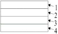
图1是本发明中紫外LED芯片散热复合基板的结构示意图。FIG. 1 is a schematic structural diagram of the ultraviolet LED chip heat dissipation composite substrate in the present invention.
具体实施方式Detailed ways
下面详细描述本发明的实施方式,所述实施方式的示例在附图中示出,其中自始至终相同或类似的标号表示相同或类似的元件或具有相同或类似功能的元件。下面通过参考附图描述的实施方式是示例性的,仅用于解释本发明,而不能理解为对本发明的限制。Embodiments of the present invention are described in detail below, examples of which are illustrated in the accompanying drawings, wherein the same or similar reference numerals refer to the same or similar elements or elements having the same or similar functions throughout. The embodiments described below with reference to the accompanying drawings are exemplary, only used to explain the present invention, and should not be construed as a limitation of the present invention.
在本发明的描述中,需要理解的是,术语“中心”、“纵向”、“横向”、“长度”、“宽度”、“厚度”、“上”、“下”、“前”、“后”、“左”、“右”、“竖直”、“水平”、“顶”、“底”、“内”、“外”、“顺时针”、“逆时针”等指示的方位或位置关系为基于附图所示的方位或位置关系,仅是为了便于描述本发明和简化描述,而不是指示或暗示所指的装置或元件必须具有特定的方位、以特定的方位构造和操作,因此不能理解为对本发明的限制。此外,术语“第一”、“第二”仅用于描述目的,而不能理解为指示或暗示相对重要性或者隐含指明所指示的技术特征的数量。由此,限定有“第一”、“第二”的特征可以明示或者隐含地包括一个或者更多个所述特征。在本发明的描述中,“多个”的含义是两个或两个以上,除非另有明确具体的限定。In the description of the present invention, it should be understood that the terms "center", "longitudinal", "lateral", "length", "width", "thickness", "upper", "lower", "front", " rear, left, right, vertical, horizontal, top, bottom, inside, outside, clockwise, counterclockwise, etc., or The positional relationship is based on the orientation or positional relationship shown in the accompanying drawings, which is only for the convenience of describing the present invention and simplifying the description, rather than indicating or implying that the referred device or element must have a specific orientation, be constructed and operated in a specific orientation, Therefore, it should not be construed as a limitation of the present invention. In addition, the terms "first" and "second" are only used for descriptive purposes, and should not be construed as indicating or implying relative importance or implying the number of indicated technical features. Thus, features defined as "first", "second" may expressly or implicitly include one or more of said features. In the description of the present invention, "plurality" means two or more, unless otherwise expressly and specifically defined.
在本发明的描述中,需要说明的是,除非另有明确的规定和限定,术语“安装”、“相连”、“连接”应做广义理解,例如,可以是固定连接,也可以是可拆卸连接,或一体地连接;可以是机械连接,也可以是电连接或可以相互通讯;可以是直接相连,也可以通过中间媒介间接相连,可以是两个元件内部的连通或两个元件的相互作用关系。对于本领域的普通技术人员而言,可以根据具体情况理解上述术语在本发明中的具体含义。In the description of the present invention, it should be noted that the terms "installed", "connected" and "connected" should be understood in a broad sense, unless otherwise expressly specified and limited, for example, it may be a fixed connection or a detachable connection Connection, or integral connection; it can be mechanical connection, electrical connection or can communicate with each other; it can be directly connected or indirectly connected through an intermediate medium, it can be the internal communication of two elements or the interaction of two elements relation. For those of ordinary skill in the art, the specific meanings of the above terms in the present invention can be understood according to specific situations.
在本发明中,除非另有明确的规定和限定,第一特征在第二特征之“上”或之“下”可以包括第一和第二特征直接接触,也可以包括第一和第二特征不是直接接触而是通过它们之间的另外的特征接触。而且,第一特征在第二特征“之上”、“上方”和“上面”包括第一特征在第二特征正上方和斜上方,或仅仅表示第一特征水平高度高于第二特征。第一特征在第二特征“之下”、“下方”和“下面”包括第一特征在第二特征正下方和斜下方,或仅仅表示第一特征水平高度小于第二特征。In the present invention, unless otherwise expressly specified and limited, a first feature "on" or "under" a second feature may include the first and second features in direct contact, or may include the first and second features Not directly but through additional features between them. Also, the first feature being "above", "over" and "above" the second feature includes the first feature being directly above and obliquely above the second feature, or simply means that the first feature is level higher than the second feature. The first feature is "below", "below" and "below" the second feature includes the first feature being directly below and diagonally below the second feature, or simply means that the first feature has a lower level than the second feature.
下文的公开提供了许多不同的实施方式或例子用来实现本发明的不同结构。为了简化本发明的公开,下文中对特定例子的部件和设置进行描述。当然,它们仅仅为示例,并且目的不在于限制本发明。此外,本发明可以在不同例子中重复参考数字和/或参考字母,这种重复是为了简化和清楚的目的,其本身不指示所讨论各种实施方式和/或设置之间的关系。此外,本发明提供了的各种特定的工艺和材料的例子,但是本领域普通技术人员可以意识到其他工艺的应用和/或其他材料的使用。The following disclosure provides many different embodiments or examples for implementing different structures of the present invention. In order to simplify the disclosure of the present invention, the components and arrangements of specific examples are described below. Of course, they are only examples and are not intended to limit the invention. Furthermore, the present disclosure may repeat reference numerals and/or reference letters in different instances for the purpose of simplicity and clarity and not in itself indicative of a relationship between the various embodiments and/or arrangements discussed. In addition, the present disclosure provides examples of various specific processes and materials, but one of ordinary skill in the art will recognize the application of other processes and/or the use of other materials.
如图1所示,一种紫外LED芯片散热复合基板,包括由上到下依次设置的SiC导热层1、金刚石导热层2、石墨烯导热层3和氮化铝单晶导热层4。As shown in FIG. 1 , an ultraviolet LED chip heat dissipation composite substrate includes a SiC
本技术方案中,利用多层的高导热率材料形成的散热复合基板,可以快速实现热能在横向及纵向方向的传播,提高紫外LED芯片的散热效率,降低紫外LED由于热堆积带来的效率降低及封装结构老化。In this technical solution, the heat dissipation composite substrate formed by using multiple layers of high thermal conductivity materials can quickly realize the spread of heat energy in the lateral and longitudinal directions, improve the heat dissipation efficiency of the UV LED chip, and reduce the efficiency reduction of the UV LED due to thermal accumulation. and packaging structure aging.
在某些具体实施例中,所述SiC导热层1、金刚石导热层2、石墨烯导热层3和氮化铝单晶导热层4相邻导热层之间通过高导热的导热粘结剂粘结。In some specific embodiments, the SiC thermally
在某些具体实施例中,所述SiC导热层1的位错密度大于1020cm-3,SiC导热层1的为立方相SiC单晶结构。In some specific embodiments, the dislocation density of the SiC thermally
在某些具体实施例中,所述SiC导热层1的位错密度大于1020cm-3,SiC导热层1的为六方相SiC单晶结构。In some specific embodiments, the dislocation density of the SiC thermally
在某些具体实施例中,所述SiC导热层1的位错密度大于1020cm-3,SiC导热层1为立方相SiC单晶与六方相SiC单晶交叠形成的超晶格结构,其中立方相SiC单晶是六方相SiC单晶厚度的1.37~3.96倍;其中立方相SiC单晶与六方相SiC单晶形成的超晶格结构的总厚度大于100微米小于200微米。In some specific embodiments, the dislocation density of the SiC thermally
在某些具体实施例中,所述金刚石导热层2的位错密度大于1017cm-3,金刚石导热层2为n型金刚石导热层或p型金刚石导热层或绝缘金刚石导热层;金刚石导热层2的厚度大于100微米小于200微米。In some specific embodiments, the dislocation density of the diamond thermally conductive layer 2 is greater than 1017 cm-3 , and the diamond thermally conductive layer 2 is an n-type diamond thermally conductive layer or a p-type diamond thermally conductive layer or an insulating diamond thermally conductive layer; 2 The thickness is greater than 100 microns and less than 200 microns.
在某些具体实施例中,所述石墨烯导热层3的位错密度大于1017cm-3,石墨烯导热层3为n型石墨烯导热层或p型石墨烯导热层;石墨烯导热层3的厚度大于1纳米小于200纳米。In some specific embodiments, the dislocation density of the graphene thermally conductive layer 3 is greater than 1017 cm-3 , and the graphene thermally conductive layer 3 is an n-type graphene thermally conductive layer or a p-type graphene thermally conductive layer; the graphene thermally conductive layer 3 The thickness is greater than 1 nanometer and less than 200 nanometers.
在某些具体实施例中,所述氮化铝单晶导热层4的位错密度大于1017cm-3,氮化铝单晶导热层4为n型氮化铝单晶导热层或p型氮化铝单晶导热层或绝缘氮化铝单晶导热层;氮化铝单晶导热层4的厚度大于100微米小于200微米;氮化铝单晶导热层4中氮化铝单晶的晶区取向为m晶面或a晶面或c晶面。In some specific embodiments, the dislocation density of the aluminum nitride single crystal thermal conductive layer 4 is greater than 1017 cm−3 , and the aluminum nitride single crystal thermal conductive layer 4 is an n-type aluminum nitride single crystal thermal conductive layer or a p-type thermal conductive layer. The aluminum nitride single crystal heat-conducting layer or insulating aluminum nitride single-crystal heat-conducting layer; the thickness of the aluminum nitride single-crystal heat-conducting layer 4 is greater than 100 microns and less than 200 microns; The domain orientation is m-plane or a-plane or c-plane.
在本说明书的描述中,参考术语“一个实施方式”、“某些实施方式”、“示意性实施方式”、“示例”、“具体示例”、或“一些示例”等的描述意指结合所述实施方式或示例描述的具体特征、结构、材料或者特点包含于本发明的至少一个实施方式或示例中。在本说明书中,对上述术语的示意性表述不一定指的是相同的实施方式或示例。而且,描述的具体特征、结构、材料或者特点可以在任何的一个或多个实施方式或示例中以合适的方式结合。In the description of this specification, reference to the terms "one embodiment," "some embodiments," "exemplary embodiment," "example," "specific example," or "some examples", etc. A particular feature, structure, material, or characteristic described in this embodiment or example is included in at least one embodiment or example of the present invention. In this specification, schematic representations of the above terms do not necessarily refer to the same embodiment or example. Furthermore, the particular features, structures, materials or characteristics described may be combined in any suitable manner in any one or more embodiments or examples.
应当理解的是,本发明的应用不限于上述的举例,对本领域普通技术人员来说,可以根据上述说明加以改进或变换,所有这些改进和变换都应属于本发明所附权利要求的保护范围。It should be understood that the application of the present invention is not limited to the above examples. For those of ordinary skill in the art, improvements or transformations can be made according to the above descriptions, and all these improvements and transformations should belong to the protection scope of the appended claims of the present invention.
Claims (9)
Priority Applications (1)
| Application Number | Priority Date | Filing Date | Title |
|---|---|---|---|
| CN202010763408.XACN111769191B (en) | 2020-07-31 | 2020-07-31 | Ultraviolet LED chip heat dissipation composite substrate |
Applications Claiming Priority (1)
| Application Number | Priority Date | Filing Date | Title |
|---|---|---|---|
| CN202010763408.XACN111769191B (en) | 2020-07-31 | 2020-07-31 | Ultraviolet LED chip heat dissipation composite substrate |
Publications (2)
| Publication Number | Publication Date |
|---|---|
| CN111769191Atrue CN111769191A (en) | 2020-10-13 |
| CN111769191B CN111769191B (en) | 2022-04-08 |
Family
ID=72728176
Family Applications (1)
| Application Number | Title | Priority Date | Filing Date |
|---|---|---|---|
| CN202010763408.XAActiveCN111769191B (en) | 2020-07-31 | 2020-07-31 | Ultraviolet LED chip heat dissipation composite substrate |
Country Status (1)
| Country | Link |
|---|---|
| CN (1) | CN111769191B (en) |
Cited By (2)
| Publication number | Priority date | Publication date | Assignee | Title |
|---|---|---|---|---|
| CN112151479A (en)* | 2020-11-24 | 2020-12-29 | 度亘激光技术(苏州)有限公司 | Heat sink for device, semiconductor device and preparation method of heat sink for device |
| CN114420831A (en)* | 2021-11-22 | 2022-04-29 | 广东职业技术学院 | A kind of LED display device and its preparation method and application |
Citations (12)
| Publication number | Priority date | Publication date | Assignee | Title |
|---|---|---|---|---|
| US5392982A (en)* | 1988-11-29 | 1995-02-28 | Li; Chou H. | Ceramic bonding method |
| US20020096106A1 (en)* | 2001-01-19 | 2002-07-25 | Kub Francis J. | Electronic device with composite substrate |
| JP2010098135A (en)* | 2008-10-16 | 2010-04-30 | Sumitomo Electric Ind Ltd | Surface light emitting device and method of manufacturing the same |
| US20110001148A1 (en)* | 2009-07-06 | 2011-01-06 | Zhuo Sun | Thin flat solid state light source module |
| CN102456781A (en)* | 2010-10-21 | 2012-05-16 | 旭明光电股份有限公司 | Light emitting diode package and method of manufacturing the same |
| CN102473683A (en)* | 2009-07-15 | 2012-05-23 | Io半导体公司 | Semiconductor-on-insulator with backside heat dissipation |
| CN105140281A (en)* | 2015-05-27 | 2015-12-09 | 苏州能讯高能半导体有限公司 | Semiconductor device and manufacturing method thereof |
| CN107112329A (en)* | 2014-11-13 | 2017-08-29 | 高通股份有限公司 | The semiconductor on insulator of variable topological structure is answered with dorsal part |
| CN107852842A (en)* | 2015-07-31 | 2018-03-27 | 莱尔德技术股份有限公司 | For the multipurpose multifunctional operating system and offer heat management of electronic installation and the correlation technique of plate electrode shielding |
| CN109314363A (en)* | 2016-04-26 | 2019-02-05 | 恩耐公司 | Low size and weight, high power fiber laser pump |
| CN111196878A (en)* | 2018-11-20 | 2020-05-26 | 通用汽车环球科技运作有限责任公司 | Cured in place lightweight thermal interface |
| CN111226314A (en)* | 2018-07-27 | 2020-06-02 | 无锡艾克柏国际微电子科技有限公司 | Multilayer compound semiconductor substrate structure and preparation method thereof |
- 2020
- 2020-07-31CNCN202010763408.XApatent/CN111769191B/enactiveActive
Patent Citations (12)
| Publication number | Priority date | Publication date | Assignee | Title |
|---|---|---|---|---|
| US5392982A (en)* | 1988-11-29 | 1995-02-28 | Li; Chou H. | Ceramic bonding method |
| US20020096106A1 (en)* | 2001-01-19 | 2002-07-25 | Kub Francis J. | Electronic device with composite substrate |
| JP2010098135A (en)* | 2008-10-16 | 2010-04-30 | Sumitomo Electric Ind Ltd | Surface light emitting device and method of manufacturing the same |
| US20110001148A1 (en)* | 2009-07-06 | 2011-01-06 | Zhuo Sun | Thin flat solid state light source module |
| CN102473683A (en)* | 2009-07-15 | 2012-05-23 | Io半导体公司 | Semiconductor-on-insulator with backside heat dissipation |
| CN102456781A (en)* | 2010-10-21 | 2012-05-16 | 旭明光电股份有限公司 | Light emitting diode package and method of manufacturing the same |
| CN107112329A (en)* | 2014-11-13 | 2017-08-29 | 高通股份有限公司 | The semiconductor on insulator of variable topological structure is answered with dorsal part |
| CN105140281A (en)* | 2015-05-27 | 2015-12-09 | 苏州能讯高能半导体有限公司 | Semiconductor device and manufacturing method thereof |
| CN107852842A (en)* | 2015-07-31 | 2018-03-27 | 莱尔德技术股份有限公司 | For the multipurpose multifunctional operating system and offer heat management of electronic installation and the correlation technique of plate electrode shielding |
| CN109314363A (en)* | 2016-04-26 | 2019-02-05 | 恩耐公司 | Low size and weight, high power fiber laser pump |
| CN111226314A (en)* | 2018-07-27 | 2020-06-02 | 无锡艾克柏国际微电子科技有限公司 | Multilayer compound semiconductor substrate structure and preparation method thereof |
| CN111196878A (en)* | 2018-11-20 | 2020-05-26 | 通用汽车环球科技运作有限责任公司 | Cured in place lightweight thermal interface |
Cited By (3)
| Publication number | Priority date | Publication date | Assignee | Title |
|---|---|---|---|---|
| CN112151479A (en)* | 2020-11-24 | 2020-12-29 | 度亘激光技术(苏州)有限公司 | Heat sink for device, semiconductor device and preparation method of heat sink for device |
| CN112151479B (en)* | 2020-11-24 | 2021-02-12 | 度亘激光技术(苏州)有限公司 | Device heat sink, semiconductor device and preparation method of device heat sink |
| CN114420831A (en)* | 2021-11-22 | 2022-04-29 | 广东职业技术学院 | A kind of LED display device and its preparation method and application |
Also Published As
| Publication number | Publication date |
|---|---|
| CN111769191B (en) | 2022-04-08 |
Similar Documents
| Publication | Publication Date | Title |
|---|---|---|
| TWI460265B (en) | Thermally conductive composite material and its derived light-emitting diode | |
| US7766514B2 (en) | Light emitting diode lamp with high heat-dissipation capacity | |
| US10094537B2 (en) | Color conversion arrangement, a lighting unit, a solid state light emitter package and a luminaire | |
| WO2012015530A2 (en) | Phosphor layer having enhanced thermal conduction and light sources utilizing the phosphor layer | |
| CN111769191B (en) | Ultraviolet LED chip heat dissipation composite substrate | |
| Xie et al. | Manipulating heat transport of photoluminescent composites in LEDs/LDs | |
| Zhou et al. | White-light-emitting diodes from directional heat-conducting hexagonal boron nitride quantum dots | |
| CN105261695B (en) | A kind of bonding structure for III-V compound device | |
| US20110261571A1 (en) | Heat dissipation assisting apparatus for lamp | |
| CN106352249B (en) | High-efficiency heat-dissipation LED lamp | |
| CN1564404A (en) | Silicon chip microtunnel cooled large power laser LED array | |
| US20140084318A1 (en) | Light emitting device package and package substrate | |
| CN101276861B (en) | led | |
| CN114171659B (en) | Deep ultraviolet thin film LED with high luminous efficiency and preparation method thereof | |
| KR101156736B1 (en) | The radiating heat module for LED fish-luring lamp | |
| CN201100917Y (en) | High-efficiency LED packaging structure | |
| TW201105185A (en) | Light emitting diode (LED) structure with apertures and circuit substrate thereof | |
| WO2023279241A1 (en) | Led chip, led array and electronic device | |
| CN103117356A (en) | Carbon nanometer tube array based chip radiating method | |
| Doan et al. | Vertical GaN based light-emitting diodes on metal alloy substrate for solid state lighting application | |
| CN111769187B (en) | Ultraviolet LED chip structure | |
| KR102712120B1 (en) | HBN-based semiconductor device with high heat-dissipation property and manufacturing method thereof | |
| CN111769184A (en) | A UV LED chip protection structure | |
| CN101859833A (en) | Light-emitting component with reflective layer and structure of reflective layer thereof | |
| CN111769188A (en) | A Novel Preparation Method of Ultraviolet LED Chip Electrode |
Legal Events
| Date | Code | Title | Description |
|---|---|---|---|
| PB01 | Publication | ||
| PB01 | Publication | ||
| SE01 | Entry into force of request for substantive examination | ||
| SE01 | Entry into force of request for substantive examination | ||
| GR01 | Patent grant | ||
| GR01 | Patent grant |