CN111758144B - Ion milling device and ion source adjustment method of the ion milling device - Google Patents
Ion milling device and ion source adjustment method of the ion milling deviceDownload PDFInfo
- Publication number
- CN111758144B CN111758144BCN201880090114.6ACN201880090114ACN111758144BCN 111758144 BCN111758144 BCN 111758144BCN 201880090114 ACN201880090114 ACN 201880090114ACN 111758144 BCN111758144 BCN 111758144B
- Authority
- CN
- China
- Prior art keywords
- ion source
- ion
- sample
- ion beam
- conductive material
- Prior art date
- Legal status (The legal status is an assumption and is not a legal conclusion. Google has not performed a legal analysis and makes no representation as to the accuracy of the status listed.)
- Active
Links
Images


Classifications
- H—ELECTRICITY
- H01—ELECTRIC ELEMENTS
- H01J—ELECTRIC DISCHARGE TUBES OR DISCHARGE LAMPS
- H01J37/00—Discharge tubes with provision for introducing objects or material to be exposed to the discharge, e.g. for the purpose of examination or processing thereof
- H01J37/02—Details
- H01J37/04—Arrangements of electrodes and associated parts for generating or controlling the discharge, e.g. electron-optical arrangement or ion-optical arrangement
- H01J37/08—Ion sources; Ion guns
- H—ELECTRICITY
- H01—ELECTRIC ELEMENTS
- H01J—ELECTRIC DISCHARGE TUBES OR DISCHARGE LAMPS
- H01J37/00—Discharge tubes with provision for introducing objects or material to be exposed to the discharge, e.g. for the purpose of examination or processing thereof
- H01J37/02—Details
- H01J37/20—Means for supporting or positioning the object or the material; Means for adjusting diaphragms or lenses associated with the support
- H—ELECTRICITY
- H01—ELECTRIC ELEMENTS
- H01J—ELECTRIC DISCHARGE TUBES OR DISCHARGE LAMPS
- H01J37/00—Discharge tubes with provision for introducing objects or material to be exposed to the discharge, e.g. for the purpose of examination or processing thereof
- H01J37/02—Details
- H01J37/023—Means for mechanically adjusting components not otherwise provided for
- H—ELECTRICITY
- H01—ELECTRIC ELEMENTS
- H01J—ELECTRIC DISCHARGE TUBES OR DISCHARGE LAMPS
- H01J37/00—Discharge tubes with provision for introducing objects or material to be exposed to the discharge, e.g. for the purpose of examination or processing thereof
- H01J37/02—Details
- H01J37/04—Arrangements of electrodes and associated parts for generating or controlling the discharge, e.g. electron-optical arrangement or ion-optical arrangement
- H01J37/147—Arrangements for directing or deflecting the discharge along a desired path
- H01J37/1472—Deflecting along given lines
- H—ELECTRICITY
- H01—ELECTRIC ELEMENTS
- H01J—ELECTRIC DISCHARGE TUBES OR DISCHARGE LAMPS
- H01J37/00—Discharge tubes with provision for introducing objects or material to be exposed to the discharge, e.g. for the purpose of examination or processing thereof
- H01J37/02—Details
- H01J37/21—Means for adjusting the focus
- H—ELECTRICITY
- H01—ELECTRIC ELEMENTS
- H01J—ELECTRIC DISCHARGE TUBES OR DISCHARGE LAMPS
- H01J37/00—Discharge tubes with provision for introducing objects or material to be exposed to the discharge, e.g. for the purpose of examination or processing thereof
- H01J37/02—Details
- H01J37/24—Circuit arrangements not adapted to a particular application of the tube and not otherwise provided for
- H01J37/243—Beam current control or regulation circuits
- H—ELECTRICITY
- H01—ELECTRIC ELEMENTS
- H01J—ELECTRIC DISCHARGE TUBES OR DISCHARGE LAMPS
- H01J37/00—Discharge tubes with provision for introducing objects or material to be exposed to the discharge, e.g. for the purpose of examination or processing thereof
- H01J37/02—Details
- H01J37/244—Detectors; Associated components or circuits therefor
- H—ELECTRICITY
- H01—ELECTRIC ELEMENTS
- H01J—ELECTRIC DISCHARGE TUBES OR DISCHARGE LAMPS
- H01J37/00—Discharge tubes with provision for introducing objects or material to be exposed to the discharge, e.g. for the purpose of examination or processing thereof
- H01J37/30—Electron-beam or ion-beam tubes for localised treatment of objects
- H01J37/304—Controlling tubes by information coming from the objects or from the beam, e.g. correction signals
- H01J37/3045—Object or beam position registration
- H—ELECTRICITY
- H01—ELECTRIC ELEMENTS
- H01J—ELECTRIC DISCHARGE TUBES OR DISCHARGE LAMPS
- H01J37/00—Discharge tubes with provision for introducing objects or material to be exposed to the discharge, e.g. for the purpose of examination or processing thereof
- H01J37/30—Electron-beam or ion-beam tubes for localised treatment of objects
- H01J37/305—Electron-beam or ion-beam tubes for localised treatment of objects for casting, melting, evaporating, or etching
- H—ELECTRICITY
- H01—ELECTRIC ELEMENTS
- H01J—ELECTRIC DISCHARGE TUBES OR DISCHARGE LAMPS
- H01J37/00—Discharge tubes with provision for introducing objects or material to be exposed to the discharge, e.g. for the purpose of examination or processing thereof
- H01J37/30—Electron-beam or ion-beam tubes for localised treatment of objects
- H01J37/31—Electron-beam or ion-beam tubes for localised treatment of objects for cutting or drilling
- H—ELECTRICITY
- H01—ELECTRIC ELEMENTS
- H01J—ELECTRIC DISCHARGE TUBES OR DISCHARGE LAMPS
- H01J2237/00—Discharge tubes exposing object to beam, e.g. for analysis treatment, etching, imaging
- H01J2237/15—Means for deflecting or directing discharge
- H01J2237/1502—Mechanical adjustments
- H—ELECTRICITY
- H01—ELECTRIC ELEMENTS
- H01J—ELECTRIC DISCHARGE TUBES OR DISCHARGE LAMPS
- H01J2237/00—Discharge tubes exposing object to beam, e.g. for analysis treatment, etching, imaging
- H01J2237/20—Positioning, supporting, modifying or maintaining the physical state of objects being observed or treated
- H01J2237/202—Movement
- H01J2237/20214—Rotation
- H—ELECTRICITY
- H01—ELECTRIC ELEMENTS
- H01J—ELECTRIC DISCHARGE TUBES OR DISCHARGE LAMPS
- H01J2237/00—Discharge tubes exposing object to beam, e.g. for analysis treatment, etching, imaging
- H01J2237/245—Detection characterised by the variable being measured
- H01J2237/24564—Measurements of electric or magnetic variables, e.g. voltage, current, frequency
- H—ELECTRICITY
- H01—ELECTRIC ELEMENTS
- H01J—ELECTRIC DISCHARGE TUBES OR DISCHARGE LAMPS
- H01J2237/00—Discharge tubes exposing object to beam, e.g. for analysis treatment, etching, imaging
- H01J2237/30—Electron or ion beam tubes for processing objects
- H01J2237/304—Controlling tubes
- H01J2237/30472—Controlling the beam
Landscapes
- Chemical & Material Sciences (AREA)
- Analytical Chemistry (AREA)
- Physics & Mathematics (AREA)
- Engineering & Computer Science (AREA)
- Plasma & Fusion (AREA)
- Sampling And Sample Adjustment (AREA)
- Coating Apparatus (AREA)
Abstract
Description
Translated fromChinese技术领域technical field
本发明涉及离子铣削装置及离子铣削装置的离子源调整方法。The invention relates to an ion milling device and an ion source adjustment method of the ion milling device.
背景技术Background technique
为了观察、分析试样的内部构造,需要使设为目的的内部构造在表面露出。以往具有通过切割、机械研磨制作试样的方法,但这些方法无法避免因对试样施加物理的压力而引起的变形、损伤的产生。离子铣削装置向试样(例如,金属、半导体、玻璃、陶瓷等)的表面或截面照射加速到例如数kV的非聚焦的氩离子束,能够利用溅射现象无应力地将试样表面的原子弹飞,使试样表面平滑化。由于进行用于利用以扫描电子显微镜(SEM:ScanningElectron Microscope)、透射式电子显微镜透(TEM:Transmission Electron Microscope)为代表的电子显微镜观察试样的表面或截面的平滑加工,因此这是优异的特性。In order to observe and analyze the internal structure of a sample, it is necessary to expose the intended internal structure on the surface. Conventionally, there are methods of preparing samples by cutting and mechanical grinding, but these methods cannot avoid the occurrence of deformation and damage caused by applying physical pressure to the samples. The ion milling device irradiates the surface or cross section of the sample (such as metal, semiconductor, glass, ceramics, etc.) with a non-focused argon ion beam accelerated to, for example, several kV, and can use the sputtering phenomenon to unstress the atomic bomb on the surface of the sample. Fly to smooth the surface of the sample. This is an excellent characteristic because it performs smooth processing for observing the surface or cross section of a sample with an electron microscope typified by a scanning electron microscope (SEM: Scanning Electron Microscope) and a transmission electron microscope (TEM: Transmission Electron Microscope). .
在离子铣削装置中,为了在真空氛围中进行试样的加工,产生离子束的离子束照射部安装于真空容器。若加工试样,则从加工面产生的来自于试样的微小粒子附着于离子束照射部,因此离子铣削装置需要进行定期的清扫。因此,构成为,从真空容器卸下离子束照射部,在维护后再次安装,但是,再安装时,有可能离子束照射部产生安装误差,从离子束照射部照射的离子束的照射方向与之前发生改变。In the ion milling apparatus, in order to process a sample in a vacuum atmosphere, an ion beam irradiation unit that generates an ion beam is attached to a vacuum container. When a sample is processed, fine particles originating from the sample generated from the processed surface adhere to the ion beam irradiated portion, and therefore the ion milling apparatus needs to be cleaned periodically. Therefore, the configuration is such that the ion beam irradiation unit is detached from the vacuum container and reinstalled after maintenance. However, when reinstalling, an installation error may occur in the ion beam irradiation unit. changed before.
专利文献1公开了一种离子束照射装置,其将试样(在此为基板)保持于基板保持件,并使其以横切离子束的照射区域的方式进行往复运动,离子束照射部向基板照射离子束。对于上述的课题,在正对离子束照射部的真空容器壁面设置测量照射的离子束的束电流密度分布的离子束测量机构。利用离子束测量机构测量离子束中心位置,将基板的往复运动的行程中心位置设定于离子束中心位置或基于该位置确定的预定位置,由此,即使离子束照射部产生了安装误差,也可保证对基板的离子照射量的均一性。Patent Document 1 discloses an ion beam irradiation device that holds a sample (here, a substrate) on a substrate holder and reciprocates so as to traverse the irradiation area of the ion beam. The substrate is irradiated with an ion beam. To solve the above-mentioned problems, an ion beam measurement mechanism for measuring the beam current density distribution of the irradiated ion beam is installed on the wall surface of the vacuum chamber facing the ion beam irradiation section. The center position of the ion beam is measured by the ion beam measuring mechanism, and the stroke center position of the reciprocating motion of the substrate is set at the center position of the ion beam or a predetermined position determined based on the position, so that even if a mounting error occurs in the ion beam irradiation part, The uniformity of ion irradiation dose to the substrate can be ensured.
另一方面,在近年的半导体设备中,集成度飞跃性地提高,因此正在研发将具有细微的立体构造的图案三维地集成的半导体设备。为了进行集成这样的立体构造(三维构造)图案的设备的制造管理,需要评价截面方向的图案。专利文献2公开了如下技术:为了实现这样的立体构造图案的深度方向(或者高度方向)的高精度的测量,在试样表面形成倾斜面,进行图案的深度方向(高度方向)的测量。On the other hand, in recent semiconductor devices, the degree of integration has dramatically increased, and thus semiconductor devices in which patterns having fine three-dimensional structures are three-dimensionally integrated are being developed. In order to perform manufacturing management of a device incorporating such a three-dimensional structure (three-dimensional structure) pattern, it is necessary to evaluate the pattern in the cross-sectional direction.
现有技术文献prior art literature
专利文献patent documents
专利文献1:日本特开2017-199554号公报Patent Document 1: Japanese Patent Laid-Open No. 2017-199554
专利文献2:国际公开第2016/002341号Patent Document 2: International Publication No. 2016/002341
发明内容Contents of the invention
发明所要解决的课题The problem to be solved by the invention
专利文献2中,为了在试样表面形成用于使立体构造图案的截面露出的倾斜面,使用了聚焦离子束(FIB:Focused Ion Beam)装置。但是,就聚焦离子束装置而言,加工速度慢,而且加工范围窄,因此为了在试样表面形成设为目的的倾斜面,耗费时间。因此,发明者们探讨了利用使用加工速度快的非聚焦的离子束的离子铣削装置形成倾斜面。In
在将非聚焦的离子束用于试样的加工的情况下,其加工速度依赖于向试样照射的离子束强度、具体而言,通过加速电压施加的离子的速度和离子的数量、以及离子的照射角度。在此,从离子源放出的离子束的强度理想上认为具有强度在离子束中心最高,朝向周边逐渐减小的二项分布的形状。但是,从离子源放出的离子束受构成离子源的电极部件的污浊、电极部件的消耗产生的离子数量的波动、环境引起的电场等的干扰的影响,难以持续保持照射试样的离子束强度恒定。另外,由于因试样的组成、入射角度而引起的铣削速度的差,导致凹凸形成,因此,在向试样照射非聚焦的离子束进行加工时,在离子铣削装置中,一边以离子束中心为轴使试样旋转,一边照射离子束,抑制凹凸的形成,可以得到适于电子显微镜的观察、计测的平滑的加工面。When a non-focused ion beam is used for processing a sample, the processing speed depends on the intensity of the ion beam irradiated to the sample, specifically, the speed and number of ions applied by an accelerating voltage, and the ion the irradiation angle. Here, the intensity of the ion beam emitted from the ion source is ideally considered to have a binomial distribution shape in which the intensity is highest at the center of the ion beam and gradually decreases toward the periphery. However, the ion beam emitted from the ion source is affected by the contamination of the electrode parts constituting the ion source, the fluctuation of the number of ions caused by the consumption of the electrode parts, and the interference caused by the electric field caused by the environment. It is difficult to continuously maintain the ion beam intensity for irradiating the sample. constant. In addition, unevenness is formed due to the difference in milling speed due to the composition of the sample and the angle of incidence. Therefore, when the sample is irradiated with a non-focused ion beam for processing, in the ion milling device, while the center of the ion beam is Irradiating the sample with an ion beam while rotating the sample on the axis suppresses the formation of unevenness and obtains a smooth processed surface suitable for observation and measurement with an electron microscope.
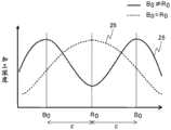
对本发明的课题进行说明。图2A示出了离子铣削装置的主要部分。具有离子源21、载置试样20的试样台22、以及使试样台22以旋转中心R0为轴沿R方向旋转的试样台旋转驱动源23。来自离子源21的离子束在以离子束中心B0为中心呈放射状扩展的状态下照射载置于试样台22的试样载置面的试样20。本来,前提是旋转中心R0和离子束中心B0一致,但有时由于离子源21的安装误差,如图2A所示地旋转中心R0和离子束中心B0成为偏离ε的状态。图2B表示此时形成于试样20的表面的加工深度。如波形25所示,在从旋转中心R0偏离ε的位置的离子束强度最高的离子束中心B0加工深度最深,随着从此分离,加工深度变小。与之相对地,将旋转中心R0和离子束中心B0一致的情况下的加工深度表示为波形26。这样,可知,由于离子源21的安装误差,加工面的形状相比本来意图的加工面顺滑地、极端的情况下,如图2B的波形25所示地,加工面波动。特别地,在为了进行微细的立体构造图案的观察、计测而有意在试样形成观察面、倾斜面的情况下,能够忽视这样的加工面的形状的变化。The subject of the present invention will be described. Fig. 2A shows the main part of the ion milling device. It includes an
此外,在图2A的例中,以离子束中心B0相对于试样20的表面(或者试样台22的试样载置面)垂直的方式照射离子束,但也可以使试样台22向C方向倾斜,将离子束以低入射角度照射试样20表面。由此,可以得到大范围的加工面。该情况下,也一边使试样台22在倾斜的状态下以旋转中心R0为轴旋转,一边向试样20照射离子束,因此,若旋转中心R0和离子束中心B0偏离(在试样20的表面上,旋转中心R0和离子束中心B0不相交),则同样地旋转中心R0与离子束中心B0的偏离变现为加工面的形状变化,存在不能得到期望的观察面、倾斜面的问题。In addition, in the example of FIG. 2A, the ion beam is irradiated so that the ion beam centerB0 is perpendicular to the surface of the sample 20 (or the sample mounting surface of the sample stage 22), but the
在如以往的装置那样采用将离子源直接安装于真空容器的结构的情况下,由于定期的清扫,需要使离子源可装卸,不能将离子源及试样室的离子源装配部的机械加工公差设为0。因此,不能避免再次安装离子源时产生错位。如使用图2A、B说明地,这导致离子铣削装置的加工精度的不均、使加工面形状的再现性降低。In the case of adopting a structure in which the ion source is directly installed in the vacuum container as in conventional devices, the ion source needs to be detachable due to periodic cleaning, and the machining tolerance of the ion source and the ion source assembly part of the sample chamber cannot be adjusted. Set to 0. Therefore, misalignment cannot be avoided when the ion source is installed again. As explained with reference to FIGS. 2A and 2B , this causes unevenness in machining accuracy of the ion milling device and reduces reproducibility of the shape of the machined surface.
另外,就离子束而言,相距离子源的射出口的距离越长,离子束径越扩展,电流、离子密度越降低。因此,可以认为,在如专利文献1那样离子束测量位置从实际的试样加工位置分离的情况下,为了测量离子束,必须使对离子源施加的电压比进行实际的加工时的条件高地进行测量。但是,若改变离子束的射出条件,则离子束具有的能量变化,因此铣削速度改变,另外,离子的密度分布也改变,进一步地,干扰施加的影响的大小也改变,因此,期望调整以与实际的加工时的射出条件相同的条件进行。因此,为了以实际的加工时的射出条件进行位置调整,有时离子铣削装置的操作人员在试样台上安装例如铜箔这样的加工对象,然后照射实际加工条件下的离子束,在铜箔上残留束痕,以使束痕和旋转中心R0一致的方式实施离子源的位置调整。但是,这样的基于束痕的目视或显微镜观察下的调整对于准确性存在界限,而且大多情况下需要反复多次离子源的装卸进行对位,实时性差,因此操作人员的调整负担大。In addition, for the ion beam, the longer the distance from the emission port of the sub-source, the wider the diameter of the ion beam and the lower the current and ion density. Therefore, it is considered that when the ion beam measurement position is separated from the actual sample processing position as in Patent Document 1, in order to measure the ion beam, it is necessary to make the voltage applied to the ion source higher than the conditions during actual processing. Measurement. However, if the emission conditions of the ion beam are changed, the energy of the ion beam changes, so the milling speed changes, and the density distribution of the ions also changes, and further, the magnitude of the influence of the interference also changes. Therefore, it is desirable to adjust to match the The injection conditions at the time of actual processing are the same as the conditions. Therefore, in order to adjust the position according to the injection conditions during actual processing, the operator of the ion milling device sometimes installs the processing object such as copper foil on the sample stage, and then irradiates the ion beam under the actual processing conditions, and the ion beam on the copper foil The beam trace remains, and the position adjustment of the ion source is performed so that the beam trace coincides with the rotation center R0 . However, there is a limit to the accuracy of such adjustments based on beam marks visually or under microscope observation, and in many cases, it is necessary to repeatedly attach and detach the ion source for alignment, and the real-time performance is poor, so the adjustment burden on the operator is heavy.
鉴于这样的课题,本发明提供可以容易且准确地调整离子源装卸后的离子束中心和试样旋转中心的离子铣削装置、及离子源调整方法。In view of such problems, the present invention provides an ion milling device and an ion source adjustment method capable of easily and accurately adjusting the ion beam center and the sample rotation center after the ion source is attached and detached.
用于解决课题的方案Solution to the problem
本发明的一实施方式的离子铣削装置通过向试样照射非聚焦的离子束,对试样进行加工,该离子铣削装置具有:试样室;设置于试样室的离子源位置调整机构;经由离子源位置调整机构安装于试样室,且射出离子束的离子源;以及以旋转中心为轴旋转的试样台,若将离子束的离子束中心和旋转中心一致时的旋转中心的延伸的方向设为Z方向,且将与Z方向垂直的面设为XY面,则离子源位置调整机构能够调整离子源的XY面上的位置及Z方向的位置。An ion milling device according to an embodiment of the present invention processes a sample by irradiating a non-focused ion beam to the sample. The ion milling device has: a sample chamber; an ion source position adjustment mechanism installed in the sample chamber; The ion source position adjustment mechanism is installed in the sample chamber, and the ion source that emits the ion beam; and the sample stage that rotates around the rotation center, if the ion beam center of the ion beam is consistent with the rotation center, the extension of the rotation center If the direction is the Z direction, and the plane perpendicular to the Z direction is the XY plane, the ion source position adjustment mechanism can adjust the position of the ion source on the XY plane and the position in the Z direction.
其它课题和新的特征根据本说明书的记载及附图将变得明了。Other subjects and new features will become apparent from the description of this specification and the accompanying drawings.
发明的效果The effect of the invention
能够提高离子铣削装置的加工精度、或加工面形状的再现精度。另外,能够缩短离子铣削装置的维护时间。The processing accuracy of the ion milling device or the reproduction accuracy of the processed surface shape can be improved. In addition, the maintenance time of the ion milling device can be shortened.
附图说明Description of drawings
图1是实施例1的离子铣削装置的主要部分结构图。FIG. 1 is a configuration diagram of main parts of an ion milling apparatus according to Example 1. FIG.
图2A是说明本发明的课题的图。FIG. 2A is a diagram illustrating the subject of the present invention.
图2B是说明本发明的课题的图。FIG. 2B is a diagram illustrating the subject of the present invention.
图3是表示试样台的结构例的图。FIG. 3 is a diagram showing a configuration example of a sample stage.
图4是离子源的位置调整的块图。FIG. 4 is a block diagram of position adjustment of an ion source.
图5是实施例1的离子源的位置调整流程。FIG. 5 is a flow chart of position adjustment of the ion source in Embodiment 1. FIG.
图6A是靶板的导电体的形状的一例。FIG. 6A is an example of the shape of the conductor of the target plate.
图6B是靶板的导电体的形状的另一例。FIG. 6B is another example of the shape of the conductor of the target plate.
图7是实施例2的离子铣削装置的主要部分结构图。FIG. 7 is a configuration diagram of main parts of an ion milling apparatus according to Example 2. FIG.
图8是实施例2的离子源的位置调整流程。FIG. 8 is a flow chart of position adjustment of the ion source in
具体实施方式Detailed ways
以下,基于附图对本发明的实施例进行说明。Hereinafter, embodiments of the present invention will be described based on the drawings.
实施例1Example 1
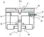
图1是实施例1的离子铣削装置的主要部分结构图。具有可保持真空状态的试样室6、离子源1、加工时设置试样(未图示)的试样台2、以及使试样台以旋转中心R0为轴向R方向旋转的试样台旋转驱动源3。此外,如图2A所示,试样台2也可以具有用于改变离子束的入射角度的倾斜机构。另外,在试样室6设有用于观察加工的试样的观察窗7。FIG. 1 is a configuration diagram of main parts of an ion milling apparatus according to Example 1. FIG. It has a
在此,离子源1经由将其位置在X方向、Y方向以及Z方向上进行微调整的离子源位置调整机构5安装于试样室6。由此,可以对离子源1的离子束中心B0的位置,具体而言,对XY面(包含X方向及Y方向的面)上的位置及动作距离(Z方向的位置,具体而言是指从离子源1的离子束放出位置到试样台2的距离)进行微调整。另外,如后述地,试样台2的试样载置板可以更换,在进行离子源1的位置调整的情况下,取代试样载置板,设置将用于检测离子束的电流的导电材4设置于含有旋转中心R0的范围的靶板。图1示出该状态。Here, the ion source 1 is attached to the
离子源位置调整机构5具有固定离子源1的支撑部、将离子源位置调整机构5设置于试样室6的基板、以及可将设于基板的支撑部在X方向、Y方向、Z方向上独立移动的离子源移动机构。作为离子源移动机构,例如,能够通过使用用于微距计那样的精密的螺纹机构将离子源1的位置在各方向上微调整。The ion source
通过对离子源1施加预定的电压,从离子源1以离子束中心B0为中心呈放射状射出离子束,照射设置于试样台2且在含有旋转中心R0的范围设有导电材4的靶板。就从离子源1射出的离子束而言,在离子束中心B0电流、离子密度高,朝向外侧,电流、离子密度逐渐降低。另外,相距离子源1的距离越长,电流、离子密度越降低。因此,使用导电材4检测离子束电流,以使离子束电流成为期望的大小的方式利用离子源位置调整机构5对离子源1的位置进行微调整,由此能够实现期望的加工精度、或加工面形状的再现精度。By applying a predetermined voltage to the ion source 1, the ion beam is radially emitted from the ion source 1 centering on the ion beam center B0 and irradiates the
图3表示试样台2的结构例。示出了设置有具有导电材4的靶板30的状态。靶板30以该导电材4与导电材连接板31连接的方式设置。此时,导电材4的中心设为用点划线表示的与旋转中心R0一致的位置。来自离子源的离子束照射以导电材4为中心的区域,但从离子源1以放射状射出离子束,因此根据离子源1与导电材4的距离不同,也存在离子束照射导电材4以外的可能性。为了防止这样的情况下因离子束照射试样台的其它结构部件而引起的电流流入导电材4,导电材4的周围的靶板30设为绝缘材。导电材连接板31连接于使试样旋转的旋转轴33,通过被试样台旋转驱动源3驱动的旋转齿轮34的动力使导电材4旋转,但为了防止导电材4受到的电流向旋转轴33流入,在导电材连接板31与旋转轴33之间设置绝缘材32,遮断电流的流动。另外,导电材4受到的电流由与导电材连接板31接触的旋转接触接点35及束电流检测配线36引出,对电流值进行检测。此外,旋转接触接点35及束电流检测配线36通过束电流检测配线连接器37与其它结构部件绝缘。FIG. 3 shows a configuration example of the
图4表示实施例1的离子铣削装置的离子源1的位置调整的块图。特别地,并非限定发明,在此表示使用基于彭宁放电的离子源作为离子源1的例。在负极电极11a、11b之间配置圆筒型的正极电极12,在负极电极11a、11b与正极电极12之间施加放电电压Vd。通过配管15将氩气导入离子源1内,通过磁铁13在正极电极12内作用磁场,由此在正极电极12内产生离子。产生的离子被施加了加速电压Va的加速电极14加速,从离子源1作为离子束放出。FIG. 4 is a block diagram showing the position adjustment of the ion source 1 of the ion milling apparatus of the first embodiment. In particular, without limiting the invention, an example using an ion source based on Penning discharge as the ion source 1 is shown here. A cylindrical positive electrode 12 is disposed between the
放电电压Vd及加速电压Va通过电源部40生成。另外,电源部40具有电流计,电流计41进行放电电流的计测,电流计42计测在导电材4受到的离子束电流。此外,放电电压Vd及加速电压Va的值由控制部45设定。The discharge voltage Vd and the acceleration voltage Va are generated by the
另外,离子源1固定于离子源位置调整机构5的支撑部16,通过可以将支撑部16在X方向、Y方向、Z方向上独立移动的离子源移动机构17,离子源1的位置可以微调整。In addition, the ion source 1 is fixed on the
电源部40、离子源移动机构17以及试样台旋转驱动源3连接于控制部45,从控制部45设定离子束射出条件,另外,根据预定的流程,执行离子源的调整、试样的加工。进一步地,控制部45连接于显示部46,显示部46作为操作人员对控制部45的用户接口发挥功能,并且进行表示控制部45收集到的离子铣削装置的动作状态的感应数据的显示等。例如,作为显示于显示部46的感应数据,包括来自电源部40的放电电压值Vd、放电电流值、加速电压值Va、离子束电流值等。The
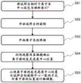
图5表示在图4所示的离子铣削装置中控制部45执行的离子源1的调整流程。FIG. 5 shows an adjustment flow of the ion source 1 executed by the
步骤S51:控制部45利用试样台旋转驱动源3开始试样台2的旋转。如图4所示,以使导电材4的表面相对于从离子源1射出的离子束垂直的方式设置试样台2。通过使试样台2旋转,能够抑制因导电材4导致的电流的检测偏差。Step S51 : The
步骤S52:控制部45控制电源部等,从离子源1向导电材4照射离子束。此时,电源部40对离子源1施加的放电电压Vd及加速电压Va按照实际加工试样时施加的电压施加条件。由此,能够高精度地再现加工试样时的离子束。Step S52 : The
步骤S53:利用电流计42计测离子束电流。控制部45获取电流计42计测出的离子束电流值。Step S53 : The ion beam current is measured by the
步骤S54:控制部45以使计测的离子束电流值满足预先决定的基准的方式控制离子源位置调整机构5。在此,离子源位置调整机构5的离子源移动机构17设为被控制部45进行马达控制,首先在X方向上移动,然后在在Y方向上移动,将离子源1的XY面上的位置调整到离子束电流值成为最大的位置。之后,根据需要使其在Z方向上移动,由此基于离子束电流值的值,对离子源1的离子束中心B0的XY面上的位置及动作距离(Z方向的位置)进行微调整。该调整例是一例,能够根据控制部45具备的算法,对离子源1的离子束中心B0的XY面上的位置及动作距离(Z方向的位置)进行微调整。Step S54: The
例如,也可以取代利用离子源位置调整机构5进行Z方向的微调整,或者在Z方向的微调整的基础上,调整对离子源1施加的放电电压值Vd。另外,进行离子源1的调整时设为目标的离子束电流值不限于离子束电流的最大值,例如,也可以确定为上次加工实施时的离子束电流值。For example, the discharge voltage value Vd applied to the ion source 1 may be adjusted instead of the fine adjustment in the Z direction by the ion source
另外,在试样台2中,也能够更换导电材4的形状不同的靶板30、或者相对于靶板30更换形状不同的导电材4。例如,图6A是作为导电材配置以旋转中心R0为中心的圆形状的导电材60的例。进一步地,即使同样的圆形状,也优选使用具有多个直径的同心圆形状的导电材的靶板。由此,能够使用具有与离子束的直径符合的检测范围的导电材进行离子源的调整。作为一例,可以使用导电材4的直径比照射靶板的离子束径小的导电材,并进行如下调整:使利用导电材4探测的离子束电流值成为最大值的方式使离子源1在Z方向上微动。In addition, in the
另一方面,图6B是作为导电材将圆形状的导电材61和直径比导电材61大的圆环形状的导电材62以旋转中心R0为中心配置成同心圆状的例。此时,由导电材61检测的离子束电流值和由导电材62检测的离子束电流值能够由电源部40独立地计测。具体而言,在试样台2设置与导电材61和导电材62对应的2系列的离子束电流引出部,由电源部40计测各个离子束电流值。由此,能够包括照射的离子束外形(能够近似成二项分布的离子束的扩展情况)进行评价,能够进一步提高离子铣削装置的加工精度、或者加工面形状的再现精度。On the other hand, FIG. 6B is an example in which a circular
对于实施例1的离子铣削装置,特别地以其离子源的位置调整为中心进行了说明,但可以进行各种变形。例如,也可以是,控制部45保留将由电流计42计测到的离子束电流值显示于显示部46,操作人员一边确认显示于显示部46的离子束电流值,一边手动调整离子源位置调整机构5的离子源移动机构17的移动量、或者离子源1的放电电压Vd。The ion milling apparatus of the first embodiment has been described focusing on the adjustment of the position of the ion source, but various modifications are possible. For example, the
实施例2Example 2
图7是实施例2的离子铣削装置的主要部分结构图。实施例2可以通过更简单的机构进行离子束中心B0与旋转中心R0的对位。在此,对于与实施例1功能相同的结构要素使用相同的符号,并省略重复的说明。FIG. 7 is a configuration diagram of main parts of an ion milling apparatus according to Example 2. FIG.
在试样室6的上方设置观察用的显微镜(光学显微镜)73,设为可以从观察窗7观察试样台2的试样载置面。另外,在试样台2的试样载置面设有镜面部件71。作为镜面部件,只要是可以反射离子源1的等离子发光的部件即可,例如,除了一般的镜子,也可以是晶圆。镜面部件只要取代试样搭载于试样台的试样载置板即可。试样台2具有倾斜机构,可以以沿X方向延伸的轴72为中心向C方向倾斜。轴72在试样台2的试样载置面位于与旋转中心R0相交的位置。图7中示出了试样台2以倾斜角T倾斜的状态。此外,倾斜角T定义为离子束中心B0与试样台2的试样载置面的法线形成的角。An observation microscope (optical microscope) 73 is provided above the
使用图8说明在这样的结构的离子铣削装置中进行离子源1的位置调整的方法。A method of adjusting the position of the ion source 1 in the ion milling apparatus having such a configuration will be described with reference to FIG. 8 .
步骤S81:使试样台2相对于离子束中心B0倾斜倾斜角T为45°。在此,试样台2的倾斜机构以轴72为中心倾斜,因此,只要是离子束中心B0和旋转中心R0一致的状态,即使改变试样台2的倾斜,与离子源1的距离也不会发生变化。因此,试样加工时,倾斜角T也可以是45°以外的期望的倾斜角。Step S81: Tilt the
步骤S82:利用试样台旋转驱动源3,开始试样台2的旋转。Step S82: Using the sample stage rotation drive
步骤S83:从离子源1向镜面部件71照射离子束。此时,电源部40对离子源1施加的放电电压Vd及加速电压Va按照实际加工试样时施加的电压施加条件。由此,能够高精度地再现加工试样时的离子束。Step S83 : Irradiating the ion beam from the ion source 1 to the
步骤S84:利用观察用显微镜73观察镜面部件71,确认从离子源1的射出口放出的等离子发光亮度的中心位置。若为离子束中心B0和旋转中心R0一致的状态,则镜面部件71的旋转中心R0附近看起来以点状或圆形状发光,若为离子束中心B0和旋转中心R0不一致的状态,则由于试样台2旋转而看起来以圆环状发光。Step S84: The
步骤S85:以使在步骤S84确认的离子源1的等离子发光亮度中心位置与试样台2的旋转中心R0一致的方式通过离子源位置调整机构5对离子源1的位置进行微调整。Step S85: Finely adjust the position of the ion source 1 by the ion source
此外,以上的例子中,设为在试样台2设置镜面部件71的方式进行了说明,但取而代之,通过设置利用离子束的照射而发光的发光部件、例如激光发光元件、或者涂敷了荧光体的试样,也可以得到同样的效果。In addition, in the above examples, the
符号说明Symbol Description
1、21—离子源,2、22—试样台,3、23—试样台旋转驱动源,4、60、61、62—导电材,5—离子源位置调整机构,6—试样室,7—观察窗,11a、11b—负极电极,12—正极电极,13—磁铁,14—加速电极,15—配管,16—支撑部,17—离子源移动机构,20—试样,30—靶板,31—导电材连接板,32—绝缘材,33—旋转轴,34—旋转齿轮,35—旋转接触接点,36—束电流检测配线,37—束电流检测配线连接器,40—电源部,41、42—电流计,45—控制部,46—显示部,71—镜面部件,72—轴,73—显微镜。1, 21—ion source, 2, 22—sample stage, 3, 23—rotation drive source of sample stage, 4, 60, 61, 62—conductive material, 5—ion source position adjustment mechanism, 6—sample chamber , 7—observation window, 11a, 11b—negative electrode, 12—positive electrode, 13—magnet, 14—accelerating electrode, 15—pipe, 16—support part, 17—ion source moving mechanism, 20—sample, 30— Target plate, 31—conductive material connecting plate, 32—insulating material, 33—rotating shaft, 34—rotating gear, 35—rotating contact point, 36—beam current detection wiring, 37—beam current detection wiring connector, 40 —power supply unit, 41, 42—galvanometer, 45—control unit, 46—display unit, 71—mirror surface component, 72—axis, 73—microscope.
Claims (15)
Priority Applications (1)
| Application Number | Priority Date | Filing Date | Title |
|---|---|---|---|
| CN202310581760.5ACN116544088A (en) | 2018-02-28 | 2018-02-28 | Ion milling device and ion source adjustment method of the ion milling device |
Applications Claiming Priority (1)
| Application Number | Priority Date | Filing Date | Title |
|---|---|---|---|
| PCT/JP2018/007477WO2019167165A1 (en) | 2018-02-28 | 2018-02-28 | Ion milling device and method for adjusting ion source of ion milling device |
Related Child Applications (1)
| Application Number | Title | Priority Date | Filing Date |
|---|---|---|---|
| CN202310581760.5ADivisionCN116544088A (en) | 2018-02-28 | 2018-02-28 | Ion milling device and ion source adjustment method of the ion milling device |
Publications (2)
| Publication Number | Publication Date |
|---|---|
| CN111758144A CN111758144A (en) | 2020-10-09 |
| CN111758144Btrue CN111758144B (en) | 2023-06-02 |
Family
ID=67806027
Family Applications (2)
| Application Number | Title | Priority Date | Filing Date |
|---|---|---|---|
| CN202310581760.5APendingCN116544088A (en) | 2018-02-28 | 2018-02-28 | Ion milling device and ion source adjustment method of the ion milling device |
| CN201880090114.6AActiveCN111758144B (en) | 2018-02-28 | 2018-02-28 | Ion milling device and ion source adjustment method of the ion milling device |
Family Applications Before (1)
| Application Number | Title | Priority Date | Filing Date |
|---|---|---|---|
| CN202310581760.5APendingCN116544088A (en) | 2018-02-28 | 2018-02-28 | Ion milling device and ion source adjustment method of the ion milling device |
Country Status (7)
| Country | Link |
|---|---|
| US (1) | US11244802B2 (en) |
| JP (2) | JP7036902B2 (en) |
| KR (2) | KR102464623B1 (en) |
| CN (2) | CN116544088A (en) |
| DE (1) | DE112018006577B4 (en) |
| TW (1) | TWI698900B (en) |
| WO (1) | WO2019167165A1 (en) |
Families Citing this family (9)
| Publication number | Priority date | Publication date | Assignee | Title |
|---|---|---|---|---|
| WO2019167165A1 (en)* | 2018-02-28 | 2019-09-06 | 株式会社日立ハイテクノロジーズ | Ion milling device and method for adjusting ion source of ion milling device |
| WO2021152726A1 (en)* | 2020-01-29 | 2021-08-05 | 株式会社日立ハイテク | Ion milling device |
| JP7312778B2 (en)* | 2021-03-08 | 2023-07-21 | 日本電子株式会社 | Sample processing device adjustment method and sample processing device |
| CN114536113B (en)* | 2022-04-27 | 2022-07-29 | 四川欧瑞特光电科技有限公司 | Negative pressure device and ion beam polishing machine |
| JP7706021B2 (en)* | 2022-06-13 | 2025-07-10 | 株式会社日立ハイテク | Ion milling apparatus, holder and cross-sectional milling method |
| CN115019994B (en)* | 2022-07-21 | 2024-05-14 | 中国核动力研究设计院 | Transmission electron microscope sample irradiation device based on ion implanter and temperature control method |
| KR20250022813A (en) | 2022-08-10 | 2025-02-17 | 주식회사 히타치하이테크 | Ion milling device and processing method using the same |
| US20250069850A1 (en)* | 2023-08-22 | 2025-02-27 | Applied Materials, Inc. | In-situ ion beam angle measurement |
| CN119309897B (en)* | 2024-12-17 | 2025-03-25 | 西安交通大学 | A method for preparing irradiated metal micro-nanomechanical samples |
Citations (7)
| Publication number | Priority date | Publication date | Assignee | Title |
|---|---|---|---|---|
| US4128765A (en)* | 1976-10-29 | 1978-12-05 | Joseph Franks | Ion beam machining techniques and apparatus |
| JPH02112138A (en)* | 1988-10-20 | 1990-04-24 | Sony Corp | Ion beam alignment method for focusing ion beam device |
| JP2008091221A (en)* | 2006-10-02 | 2008-04-17 | Hitachi High-Tech Science Systems Corp | Ion beam processing apparatus and method |
| WO2012060416A1 (en)* | 2010-11-05 | 2012-05-10 | 株式会社 日立ハイテクノロジーズ | Ion milling device |
| CN102473576A (en)* | 2009-07-30 | 2012-05-23 | 株式会社日立高新技术 | Ion milling device |
| CN104040677A (en)* | 2012-01-06 | 2014-09-10 | 株式会社日立高新技术 | Charged particle beam irradiation apparatus |
| CN104094374A (en)* | 2012-03-26 | 2014-10-08 | 株式会社日立高新技术 | ion milling device |
Family Cites Families (32)
| Publication number | Priority date | Publication date | Assignee | Title |
|---|---|---|---|---|
| JPS62143351A (en)* | 1985-12-17 | 1987-06-26 | Matsushita Electric Ind Co Ltd | Automatic optical axis adjuster |
| JPH01142149U (en)* | 1988-03-23 | 1989-09-28 | ||
| JP2985175B2 (en)* | 1988-10-17 | 1999-11-29 | ソニー株式会社 | Ion beam equipment |
| JPH0733589B2 (en)* | 1989-07-01 | 1995-04-12 | 株式会社日立サイエンスシステムズ | Ion milling method and device |
| JPH0329249A (en)* | 1990-06-12 | 1991-02-07 | Seiko Instr Inc | Converged ion beam device |
| JPH079333Y2 (en)* | 1990-11-30 | 1995-03-06 | 株式会社島津製作所 | Ion generator |
| JP3271395B2 (en)* | 1993-10-26 | 2002-04-02 | 株式会社島津製作所 | Ion beam irradiation equipment |
| JPH10134746A (en)* | 1996-10-29 | 1998-05-22 | Seiko Instr Inc | Optical axis adjustment method for focused ion beam and focused ion beam device |
| US6768110B2 (en) | 2000-06-21 | 2004-07-27 | Gatan, Inc. | Ion beam milling system and method for electron microscopy specimen preparation |
| US20060145095A1 (en)* | 2004-12-30 | 2006-07-06 | Varian Semiconductor Equipment Associates, Inc. | Methods and apparatus for ion implantation with control of incidence angle by beam deflection |
| JP2006236601A (en)* | 2005-02-22 | 2006-09-07 | Kobe Steel Ltd | Orbital position detecting device, composition analyzer, orbit adjusting method for charged particle beam and position coordinate detecting device |
| JP4504880B2 (en) | 2005-07-08 | 2010-07-14 | 株式会社日立ハイテクノロジーズ | Ion beam current measurement mechanism using cylinder using vacuum pumping system |
| JP4594193B2 (en) | 2005-08-26 | 2010-12-08 | 日本電子株式会社 | Ion milling equipment |
| WO2007067296A2 (en)* | 2005-12-02 | 2007-06-14 | Alis Corporation | Ion sources, systems and methods |
| JP2008204905A (en)* | 2007-02-22 | 2008-09-04 | Hitachi High-Tech Science Systems Corp | Ion milling apparatus and ion milling method |
| US20120217391A1 (en)* | 2009-11-06 | 2012-08-30 | Hiroyasu Shichi | Charged particle microscope |
| JP2011154920A (en)* | 2010-01-28 | 2011-08-11 | Hitachi High-Technologies Corp | Ion milling device, sample processing method, processing device, and sample driving mechanism |
| JP5989959B2 (en)* | 2010-02-16 | 2016-09-07 | 株式会社日立ハイテクサイエンス | Focused ion beam device |
| US8283642B2 (en) | 2010-04-11 | 2012-10-09 | Gatan, Inc. | Ion beam sample preparation apparatus and methods |
| US9347127B2 (en)* | 2012-07-16 | 2016-05-24 | Veeco Instruments, Inc. | Film deposition assisted by angular selective etch on a surface |
| TWI686837B (en)* | 2012-12-31 | 2020-03-01 | 美商Fei公司 | Fiducial design for tilted or glancing mill operations with a charged particle beam |
| CN105340050B (en)* | 2013-07-29 | 2017-06-06 | 株式会社日立高新技术 | Ion milling device and processing method using ion milling device |
| EP3859766A1 (en)* | 2014-04-01 | 2021-08-04 | EV Group E. Thallner GmbH | Method and device for treating surfaces on substrates |
| JP6427571B2 (en)* | 2014-06-30 | 2018-11-21 | 株式会社日立ハイテクノロジーズ | Pattern measurement method and pattern measurement apparatus |
| US10731246B2 (en) | 2014-07-28 | 2020-08-04 | Gatan, Inc. | Ion beam sample preparation and coating apparatus and methods |
| US10361065B2 (en)* | 2015-09-25 | 2019-07-23 | Hitachi High-Technologies Corporation | Ion milling system |
| JP6710270B2 (en)* | 2016-02-26 | 2020-06-17 | 株式会社日立ハイテク | Ion milling device and ion milling method |
| JP2017199554A (en) | 2016-04-27 | 2017-11-02 | 日新電機株式会社 | Ion beam irradiation device and ion beam irradiation method |
| WO2018003109A1 (en) | 2016-07-01 | 2018-01-04 | 株式会社 日立ハイテクノロジーズ | Ion-milling apparatus |
| WO2019167165A1 (en)* | 2018-02-28 | 2019-09-06 | 株式会社日立ハイテクノロジーズ | Ion milling device and method for adjusting ion source of ion milling device |
| JP6998467B2 (en)* | 2018-08-31 | 2022-01-18 | 株式会社日立ハイテク | Ion milling device |
| GB2582242A (en)* | 2018-11-30 | 2020-09-23 | Oxford Instruments Nanotechnology Tools Ltd | Charged particle beam source, surface processing apparatus and surface processing method |
- 2018
- 2018-02-28WOPCT/JP2018/007477patent/WO2019167165A1/ennot_activeCeased
- 2018-02-28JPJP2020503158Apatent/JP7036902B2/enactiveActive
- 2018-02-28CNCN202310581760.5Apatent/CN116544088A/enactivePending
- 2018-02-28USUS16/961,759patent/US11244802B2/enactiveActive
- 2018-02-28KRKR1020207019868Apatent/KR102464623B1/enactiveActive
- 2018-02-28DEDE112018006577.4Tpatent/DE112018006577B4/enactiveActive
- 2018-02-28KRKR1020227038540Apatent/KR102551000B1/enactiveActive
- 2018-02-28CNCN201880090114.6Apatent/CN111758144B/enactiveActive
- 2019
- 2019-02-25TWTW108106272Apatent/TWI698900B/enactive
- 2022
- 2022-03-03JPJP2022032598Apatent/JP7350916B2/enactiveActive
Patent Citations (8)
| Publication number | Priority date | Publication date | Assignee | Title |
|---|---|---|---|---|
| US4128765A (en)* | 1976-10-29 | 1978-12-05 | Joseph Franks | Ion beam machining techniques and apparatus |
| JPH02112138A (en)* | 1988-10-20 | 1990-04-24 | Sony Corp | Ion beam alignment method for focusing ion beam device |
| JP2008091221A (en)* | 2006-10-02 | 2008-04-17 | Hitachi High-Tech Science Systems Corp | Ion beam processing apparatus and method |
| CN102473576A (en)* | 2009-07-30 | 2012-05-23 | 株式会社日立高新技术 | Ion milling device |
| WO2012060416A1 (en)* | 2010-11-05 | 2012-05-10 | 株式会社 日立ハイテクノロジーズ | Ion milling device |
| CN105047511A (en)* | 2010-11-05 | 2015-11-11 | 株式会社日立高新技术 | Ion milling device |
| CN104040677A (en)* | 2012-01-06 | 2014-09-10 | 株式会社日立高新技术 | Charged particle beam irradiation apparatus |
| CN104094374A (en)* | 2012-03-26 | 2014-10-08 | 株式会社日立高新技术 | ion milling device |
Also Published As
| Publication number | Publication date |
|---|---|
| DE112018006577T5 (en) | 2020-11-12 |
| CN116544088A (en) | 2023-08-04 |
| JPWO2019167165A1 (en) | 2021-02-04 |
| WO2019167165A1 (en) | 2019-09-06 |
| JP2022081571A (en) | 2022-05-31 |
| JP7350916B2 (en) | 2023-09-26 |
| KR102464623B1 (en) | 2022-11-09 |
| KR102551000B1 (en) | 2023-07-05 |
| DE112018006577B4 (en) | 2024-08-01 |
| KR20220154249A (en) | 2022-11-21 |
| US20210066020A1 (en) | 2021-03-04 |
| KR20200096619A (en) | 2020-08-12 |
| US11244802B2 (en) | 2022-02-08 |
| TW201937529A (en) | 2019-09-16 |
| CN111758144A (en) | 2020-10-09 |
| TWI698900B (en) | 2020-07-11 |
| JP7036902B2 (en) | 2022-03-15 |
Similar Documents
| Publication | Publication Date | Title |
|---|---|---|
| CN111758144B (en) | Ion milling device and ion source adjustment method of the ion milling device | |
| US8334519B2 (en) | Multi-part specimen holder with conductive patterns | |
| JP2013511809A (en) | High sensitivity and high throughput electron beam inspection column enabled by adjustable beam limiting aperture | |
| KR20150110392A (en) | Focused ion beam apparatus | |
| JP2002148159A (en) | Sample preparation method and sample preparation device | |
| US11508552B2 (en) | Ion milling device | |
| KR102823067B1 (en) | Ion milling device | |
| US20020008200A1 (en) | Correction method of scanning electron microscope | |
| CN100564588C (en) | The plasma process method and apparatus | |
| JP2017228488A (en) | Method for adjusting electron beam emission direction and electron beam emitter device | |
| TWI773042B (en) | Ion Milling Device | |
| WO2024195014A1 (en) | Ion milling device and processing method using same | |
| WO2022244149A1 (en) | Ion milling device | |
| CN118553584A (en) | Ultra-precise ion mill | |
| WO2024034052A1 (en) | Ion milling device and processing method using same | |
| WO2024201722A1 (en) | Ion milling device, maintenance method, and focusing electrode for ion milling device |
Legal Events
| Date | Code | Title | Description |
|---|---|---|---|
| PB01 | Publication | ||
| PB01 | Publication | ||
| SE01 | Entry into force of request for substantive examination | ||
| SE01 | Entry into force of request for substantive examination | ||
| GR01 | Patent grant | ||
| GR01 | Patent grant |