CN111754922A - Pixel driving circuit and driving method thereof, and display panel - Google Patents
Pixel driving circuit and driving method thereof, and display panelDownload PDFInfo
- Publication number
- CN111754922A CN111754922ACN202010752675.7ACN202010752675ACN111754922ACN 111754922 ACN111754922 ACN 111754922ACN 202010752675 ACN202010752675 ACN 202010752675ACN 111754922 ACN111754922 ACN 111754922A
- Authority
- CN
- China
- Prior art keywords
- transistor
- drain
- source
- gate
- signal line
- Prior art date
- Legal status (The legal status is an assumption and is not a legal conclusion. Google has not performed a legal analysis and makes no representation as to the accuracy of the status listed.)
- Granted
Links
Images


Classifications
- G—PHYSICS
- G09—EDUCATION; CRYPTOGRAPHY; DISPLAY; ADVERTISING; SEALS
- G09G—ARRANGEMENTS OR CIRCUITS FOR CONTROL OF INDICATING DEVICES USING STATIC MEANS TO PRESENT VARIABLE INFORMATION
- G09G3/00—Control arrangements or circuits, of interest only in connection with visual indicators other than cathode-ray tubes
- G09G3/20—Control arrangements or circuits, of interest only in connection with visual indicators other than cathode-ray tubes for presentation of an assembly of a number of characters, e.g. a page, by composing the assembly by combination of individual elements arranged in a matrix no fixed position being assigned to or needed to be assigned to the individual characters or partial characters
- G09G3/22—Control arrangements or circuits, of interest only in connection with visual indicators other than cathode-ray tubes for presentation of an assembly of a number of characters, e.g. a page, by composing the assembly by combination of individual elements arranged in a matrix no fixed position being assigned to or needed to be assigned to the individual characters or partial characters using controlled light sources
- G09G3/30—Control arrangements or circuits, of interest only in connection with visual indicators other than cathode-ray tubes for presentation of an assembly of a number of characters, e.g. a page, by composing the assembly by combination of individual elements arranged in a matrix no fixed position being assigned to or needed to be assigned to the individual characters or partial characters using controlled light sources using electroluminescent panels
- G09G3/32—Control arrangements or circuits, of interest only in connection with visual indicators other than cathode-ray tubes for presentation of an assembly of a number of characters, e.g. a page, by composing the assembly by combination of individual elements arranged in a matrix no fixed position being assigned to or needed to be assigned to the individual characters or partial characters using controlled light sources using electroluminescent panels semiconductive, e.g. using light-emitting diodes [LED]
- G09G3/3208—Control arrangements or circuits, of interest only in connection with visual indicators other than cathode-ray tubes for presentation of an assembly of a number of characters, e.g. a page, by composing the assembly by combination of individual elements arranged in a matrix no fixed position being assigned to or needed to be assigned to the individual characters or partial characters using controlled light sources using electroluminescent panels semiconductive, e.g. using light-emitting diodes [LED] organic, e.g. using organic light-emitting diodes [OLED]
- G09G3/3225—Control arrangements or circuits, of interest only in connection with visual indicators other than cathode-ray tubes for presentation of an assembly of a number of characters, e.g. a page, by composing the assembly by combination of individual elements arranged in a matrix no fixed position being assigned to or needed to be assigned to the individual characters or partial characters using controlled light sources using electroluminescent panels semiconductive, e.g. using light-emitting diodes [LED] organic, e.g. using organic light-emitting diodes [OLED] using an active matrix
- G09G3/3233—Control arrangements or circuits, of interest only in connection with visual indicators other than cathode-ray tubes for presentation of an assembly of a number of characters, e.g. a page, by composing the assembly by combination of individual elements arranged in a matrix no fixed position being assigned to or needed to be assigned to the individual characters or partial characters using controlled light sources using electroluminescent panels semiconductive, e.g. using light-emitting diodes [LED] organic, e.g. using organic light-emitting diodes [OLED] using an active matrix with pixel circuitry controlling the current through the light-emitting element
- G—PHYSICS
- G09—EDUCATION; CRYPTOGRAPHY; DISPLAY; ADVERTISING; SEALS
- G09G—ARRANGEMENTS OR CIRCUITS FOR CONTROL OF INDICATING DEVICES USING STATIC MEANS TO PRESENT VARIABLE INFORMATION
- G09G3/00—Control arrangements or circuits, of interest only in connection with visual indicators other than cathode-ray tubes
- G09G3/20—Control arrangements or circuits, of interest only in connection with visual indicators other than cathode-ray tubes for presentation of an assembly of a number of characters, e.g. a page, by composing the assembly by combination of individual elements arranged in a matrix no fixed position being assigned to or needed to be assigned to the individual characters or partial characters
- G09G3/22—Control arrangements or circuits, of interest only in connection with visual indicators other than cathode-ray tubes for presentation of an assembly of a number of characters, e.g. a page, by composing the assembly by combination of individual elements arranged in a matrix no fixed position being assigned to or needed to be assigned to the individual characters or partial characters using controlled light sources
- G09G3/30—Control arrangements or circuits, of interest only in connection with visual indicators other than cathode-ray tubes for presentation of an assembly of a number of characters, e.g. a page, by composing the assembly by combination of individual elements arranged in a matrix no fixed position being assigned to or needed to be assigned to the individual characters or partial characters using controlled light sources using electroluminescent panels
- G09G3/32—Control arrangements or circuits, of interest only in connection with visual indicators other than cathode-ray tubes for presentation of an assembly of a number of characters, e.g. a page, by composing the assembly by combination of individual elements arranged in a matrix no fixed position being assigned to or needed to be assigned to the individual characters or partial characters using controlled light sources using electroluminescent panels semiconductive, e.g. using light-emitting diodes [LED]
- G09G3/3208—Control arrangements or circuits, of interest only in connection with visual indicators other than cathode-ray tubes for presentation of an assembly of a number of characters, e.g. a page, by composing the assembly by combination of individual elements arranged in a matrix no fixed position being assigned to or needed to be assigned to the individual characters or partial characters using controlled light sources using electroluminescent panels semiconductive, e.g. using light-emitting diodes [LED] organic, e.g. using organic light-emitting diodes [OLED]
- G09G3/3225—Control arrangements or circuits, of interest only in connection with visual indicators other than cathode-ray tubes for presentation of an assembly of a number of characters, e.g. a page, by composing the assembly by combination of individual elements arranged in a matrix no fixed position being assigned to or needed to be assigned to the individual characters or partial characters using controlled light sources using electroluminescent panels semiconductive, e.g. using light-emitting diodes [LED] organic, e.g. using organic light-emitting diodes [OLED] using an active matrix
- G09G3/3258—Control arrangements or circuits, of interest only in connection with visual indicators other than cathode-ray tubes for presentation of an assembly of a number of characters, e.g. a page, by composing the assembly by combination of individual elements arranged in a matrix no fixed position being assigned to or needed to be assigned to the individual characters or partial characters using controlled light sources using electroluminescent panels semiconductive, e.g. using light-emitting diodes [LED] organic, e.g. using organic light-emitting diodes [OLED] using an active matrix with pixel circuitry controlling the voltage across the light-emitting element
- G—PHYSICS
- G09—EDUCATION; CRYPTOGRAPHY; DISPLAY; ADVERTISING; SEALS
- G09G—ARRANGEMENTS OR CIRCUITS FOR CONTROL OF INDICATING DEVICES USING STATIC MEANS TO PRESENT VARIABLE INFORMATION
- G09G3/00—Control arrangements or circuits, of interest only in connection with visual indicators other than cathode-ray tubes
- G09G3/20—Control arrangements or circuits, of interest only in connection with visual indicators other than cathode-ray tubes for presentation of an assembly of a number of characters, e.g. a page, by composing the assembly by combination of individual elements arranged in a matrix no fixed position being assigned to or needed to be assigned to the individual characters or partial characters
- G09G3/22—Control arrangements or circuits, of interest only in connection with visual indicators other than cathode-ray tubes for presentation of an assembly of a number of characters, e.g. a page, by composing the assembly by combination of individual elements arranged in a matrix no fixed position being assigned to or needed to be assigned to the individual characters or partial characters using controlled light sources
- G09G3/30—Control arrangements or circuits, of interest only in connection with visual indicators other than cathode-ray tubes for presentation of an assembly of a number of characters, e.g. a page, by composing the assembly by combination of individual elements arranged in a matrix no fixed position being assigned to or needed to be assigned to the individual characters or partial characters using controlled light sources using electroluminescent panels
- G09G3/32—Control arrangements or circuits, of interest only in connection with visual indicators other than cathode-ray tubes for presentation of an assembly of a number of characters, e.g. a page, by composing the assembly by combination of individual elements arranged in a matrix no fixed position being assigned to or needed to be assigned to the individual characters or partial characters using controlled light sources using electroluminescent panels semiconductive, e.g. using light-emitting diodes [LED]
- G09G3/3208—Control arrangements or circuits, of interest only in connection with visual indicators other than cathode-ray tubes for presentation of an assembly of a number of characters, e.g. a page, by composing the assembly by combination of individual elements arranged in a matrix no fixed position being assigned to or needed to be assigned to the individual characters or partial characters using controlled light sources using electroluminescent panels semiconductive, e.g. using light-emitting diodes [LED] organic, e.g. using organic light-emitting diodes [OLED]
- G09G3/3266—Details of drivers for scan electrodes
- G—PHYSICS
- G09—EDUCATION; CRYPTOGRAPHY; DISPLAY; ADVERTISING; SEALS
- G09G—ARRANGEMENTS OR CIRCUITS FOR CONTROL OF INDICATING DEVICES USING STATIC MEANS TO PRESENT VARIABLE INFORMATION
- G09G2300/00—Aspects of the constitution of display devices
- G09G2300/04—Structural and physical details of display devices
- G09G2300/0421—Structural details of the set of electrodes
- G09G2300/0426—Layout of electrodes and connections
- G—PHYSICS
- G09—EDUCATION; CRYPTOGRAPHY; DISPLAY; ADVERTISING; SEALS
- G09G—ARRANGEMENTS OR CIRCUITS FOR CONTROL OF INDICATING DEVICES USING STATIC MEANS TO PRESENT VARIABLE INFORMATION
- G09G2300/00—Aspects of the constitution of display devices
- G09G2300/04—Structural and physical details of display devices
- G09G2300/0421—Structural details of the set of electrodes
- G09G2300/043—Compensation electrodes or other additional electrodes in matrix displays related to distortions or compensation signals, e.g. for modifying TFT threshold voltage in column driver
- G—PHYSICS
- G09—EDUCATION; CRYPTOGRAPHY; DISPLAY; ADVERTISING; SEALS
- G09G—ARRANGEMENTS OR CIRCUITS FOR CONTROL OF INDICATING DEVICES USING STATIC MEANS TO PRESENT VARIABLE INFORMATION
- G09G2300/00—Aspects of the constitution of display devices
- G09G2300/08—Active matrix structure, i.e. with use of active elements, inclusive of non-linear two terminal elements, in the pixels together with light emitting or modulating elements
- G09G2300/0809—Several active elements per pixel in active matrix panels
- G09G2300/0819—Several active elements per pixel in active matrix panels used for counteracting undesired variations, e.g. feedback or autozeroing
- G—PHYSICS
- G09—EDUCATION; CRYPTOGRAPHY; DISPLAY; ADVERTISING; SEALS
- G09G—ARRANGEMENTS OR CIRCUITS FOR CONTROL OF INDICATING DEVICES USING STATIC MEANS TO PRESENT VARIABLE INFORMATION
- G09G2300/00—Aspects of the constitution of display devices
- G09G2300/08—Active matrix structure, i.e. with use of active elements, inclusive of non-linear two terminal elements, in the pixels together with light emitting or modulating elements
- G09G2300/0809—Several active elements per pixel in active matrix panels
- G09G2300/0842—Several active elements per pixel in active matrix panels forming a memory circuit, e.g. a dynamic memory with one capacitor
- G09G2300/0861—Several active elements per pixel in active matrix panels forming a memory circuit, e.g. a dynamic memory with one capacitor with additional control of the display period without amending the charge stored in a pixel memory, e.g. by means of additional select electrodes
- G—PHYSICS
- G09—EDUCATION; CRYPTOGRAPHY; DISPLAY; ADVERTISING; SEALS
- G09G—ARRANGEMENTS OR CIRCUITS FOR CONTROL OF INDICATING DEVICES USING STATIC MEANS TO PRESENT VARIABLE INFORMATION
- G09G2310/00—Command of the display device
- G09G2310/02—Addressing, scanning or driving the display screen or processing steps related thereto
- G09G2310/0202—Addressing of scan or signal lines
- G09G2310/0216—Interleaved control phases for different scan lines in the same sub-field, e.g. initialization, addressing and sustaining in plasma displays that are not simultaneous for all scan lines
- G—PHYSICS
- G09—EDUCATION; CRYPTOGRAPHY; DISPLAY; ADVERTISING; SEALS
- G09G—ARRANGEMENTS OR CIRCUITS FOR CONTROL OF INDICATING DEVICES USING STATIC MEANS TO PRESENT VARIABLE INFORMATION
- G09G2310/00—Command of the display device
- G09G2310/02—Addressing, scanning or driving the display screen or processing steps related thereto
- G09G2310/0243—Details of the generation of driving signals
- G09G2310/0251—Precharge or discharge of pixel before applying new pixel voltage
- G—PHYSICS
- G09—EDUCATION; CRYPTOGRAPHY; DISPLAY; ADVERTISING; SEALS
- G09G—ARRANGEMENTS OR CIRCUITS FOR CONTROL OF INDICATING DEVICES USING STATIC MEANS TO PRESENT VARIABLE INFORMATION
- G09G2310/00—Command of the display device
- G09G2310/08—Details of timing specific for flat panels, other than clock recovery
- G—PHYSICS
- G09—EDUCATION; CRYPTOGRAPHY; DISPLAY; ADVERTISING; SEALS
- G09G—ARRANGEMENTS OR CIRCUITS FOR CONTROL OF INDICATING DEVICES USING STATIC MEANS TO PRESENT VARIABLE INFORMATION
- G09G2320/00—Control of display operating conditions
- G09G2320/02—Improving the quality of display appearance
- G09G2320/0233—Improving the luminance or brightness uniformity across the screen
- G—PHYSICS
- G09—EDUCATION; CRYPTOGRAPHY; DISPLAY; ADVERTISING; SEALS
- G09G—ARRANGEMENTS OR CIRCUITS FOR CONTROL OF INDICATING DEVICES USING STATIC MEANS TO PRESENT VARIABLE INFORMATION
- G09G2320/00—Control of display operating conditions
- G09G2320/02—Improving the quality of display appearance
- G09G2320/0247—Flicker reduction other than flicker reduction circuits used for single beam cathode-ray tubes
- G—PHYSICS
- G09—EDUCATION; CRYPTOGRAPHY; DISPLAY; ADVERTISING; SEALS
- G09G—ARRANGEMENTS OR CIRCUITS FOR CONTROL OF INDICATING DEVICES USING STATIC MEANS TO PRESENT VARIABLE INFORMATION
- G09G2320/00—Control of display operating conditions
- G09G2320/04—Maintaining the quality of display appearance
- G09G2320/043—Preventing or counteracting the effects of ageing
- G09G2320/045—Compensation of drifts in the characteristics of light emitting or modulating elements
- G—PHYSICS
- G09—EDUCATION; CRYPTOGRAPHY; DISPLAY; ADVERTISING; SEALS
- G09G—ARRANGEMENTS OR CIRCUITS FOR CONTROL OF INDICATING DEVICES USING STATIC MEANS TO PRESENT VARIABLE INFORMATION
- G09G2330/00—Aspects of power supply; Aspects of display protection and defect management
- G09G2330/02—Details of power systems and of start or stop of display operation
- G09G2330/021—Power management, e.g. power saving
Landscapes
- Engineering & Computer Science (AREA)
- Physics & Mathematics (AREA)
- Computer Hardware Design (AREA)
- General Physics & Mathematics (AREA)
- Theoretical Computer Science (AREA)
- Control Of El Displays (AREA)
- Control Of Indicators Other Than Cathode Ray Tubes (AREA)
- Electroluminescent Light Sources (AREA)
Abstract
Description
Translated fromChinese技术领域technical field
本申请涉及显示技术领域,尤其涉及一种像素驱动电路及其驱动方法、显示面板。The present application relates to the field of display technology, and in particular, to a pixel driving circuit and a driving method thereof, and a display panel.
背景技术Background technique
低温多晶硅技术被广泛用于显示装置中,但由于多晶硅自身存在晶粒间界和大量的间界缺陷态密度,使得各个晶体管的阈值电压不同,且在长时间栅偏压的作用下晶体管的阈值电压会发生偏移,导致显示面板显示时,显示画面会出现显示亮度不均、闪烁等问题,影响显示品质。Low-temperature polysilicon technology is widely used in display devices, but due to the existence of grain boundaries and a large number of boundary defect state densities in polysilicon itself, the threshold voltage of each transistor is different, and the threshold voltage of the transistor is under the action of long-term gate bias. The voltage will be offset, resulting in uneven display brightness and flickering of the display screen when the display panel is displayed, which affects the display quality.
发明内容SUMMARY OF THE INVENTION
本申请实施例提供一种像素驱动电路及其驱动方法、显示面板,可以补偿驱动晶体管的阈值电压,改善显示面板的显示效果。Embodiments of the present application provide a pixel driving circuit, a driving method thereof, and a display panel, which can compensate the threshold voltage of the driving transistor and improve the display effect of the display panel.
本申请实施例提供一种像素驱动电路,包括:发光器件,驱动晶体管,补偿模块及数据写入模块;所述驱动晶体管用于为所述发光器件提供驱动电流;所述补偿模块至少包括:存储电容,所述存储电容用于维持所述驱动晶体管的栅极电压;第一晶体管,所述第一晶体管的源极或漏极中的一者与所述驱动晶体管的栅极连接,所述第一晶体管用于将第一复位信号传输至所述驱动晶体管的栅极;第二晶体管,所述第二晶体管用于将第二复位信号传输至所述驱动晶体管的源极或漏极中的一者;补偿晶体管,所述存储电容串联在所述补偿晶体管的源极或漏极中的一者与所述驱动晶体管的所述栅极之间,所述补偿晶体管的所述源极或所述漏极中的另一者与所述驱动晶体管的所述源极或所述漏极中的一者连接,所述补偿晶体管用于与所述第二晶体管、所述存储电容补偿所述驱动晶体管的阈值电压;所述数据写入模块至少包括:数据写入晶体管,所述数据写入晶体管的源极或漏极中的一者与所述存储电容的上极板连接,所述数据写入晶体管用于将数据信号写入所述存储电容,并将所述数据信号传输至所述驱动晶体管的栅极。An embodiment of the present application provides a pixel driving circuit, including: a light-emitting device, a driving transistor, a compensation module, and a data writing module; the driving transistor is used to provide a driving current for the light-emitting device; the compensation module at least includes: a storage a capacitor, the storage capacitor is used to maintain the gate voltage of the driving transistor; a first transistor, one of the source or drain of the first transistor is connected to the gate of the driving transistor, the first transistor A transistor for transmitting the first reset signal to the gate of the driving transistor; a second transistor for transmitting the second reset signal to one of the source or drain of the driving transistor Or; a compensation transistor, the storage capacitor is connected in series between one of the source or drain of the compensation transistor and the gate of the drive transistor, the source of the compensation transistor or the The other one of the drains is connected to one of the source or the drain of the drive transistor, and the compensation transistor is used to compensate the drive transistor with the second transistor, the storage capacitor the threshold voltage of The transistor is used to write a data signal into the storage capacitor and transmit the data signal to the gate of the driving transistor.
本申请还提供一种像素驱动电路的驱动方法,用于驱动所述的像素驱动电路,在第N帧周期内,所述驱动方法包括:初始化阶段,所述补偿模块的所述第一晶体管将所述第一复位信号传输至所述驱动晶体管的所述栅极,初始化所述驱动晶体管的所述栅极电压,所述第二晶体管、所述补偿晶体管及所述存储电容补偿所述驱动晶体管的阈值电压;数据写入阶段,所述存储电容写入所述数据信号,并将所述数据信号传输至所述驱动晶体管的所述栅极。The present application also provides a driving method for a pixel driving circuit, which is used for driving the pixel driving circuit. In the Nth frame period, the driving method includes: an initialization stage, wherein the first transistor of the compensation module will The first reset signal is transmitted to the gate of the drive transistor to initialize the gate voltage of the drive transistor, and the second transistor, the compensation transistor and the storage capacitor compensate the drive transistor In the data writing stage, the storage capacitor writes the data signal and transmits the data signal to the gate of the driving transistor.
本申请还提供一种显示面板,包括像素驱动电路,所述像素驱动电路包括:存储电容;以及,发光器件,所述发光器件的阴极与第一电压端连接;第一晶体管,所述第一晶体管的栅极与第一扫描信号线连接,所述第一晶体管的源极或漏极中的一者与第一复位信号线连接,所述源极或所述漏极中的另一者与第八晶体管的栅极连接;第二晶体管,所述第二晶体管的栅极与所述第一扫描信号线连接,所述第二晶体管的源极或漏极中的一者与第二复位信号线连接;第三晶体管,所述第三晶体管的栅极与所述第一扫描信号线连接,所述存储电容串联在所述第三晶体管的源极或漏极中的一者与所述第八晶体管的所述栅极之间,所述第三晶体管的所述源极或所述漏极中的另一者与所述第八晶体管的源极或漏极中的一者连接;第四晶体管,所述第四晶体管的栅极与第二扫描信号线连接,所述第四晶体管的源极或漏极中的一者与数据信号线连接,所述源极或所述漏极中的另一者与所述存储电容的上极板连接。The present application also provides a display panel, comprising a pixel driving circuit, the pixel driving circuit comprising: a storage capacitor; and a light-emitting device, a cathode of the light-emitting device is connected to a first voltage terminal; a first transistor, the first The gate of the transistor is connected to the first scan signal line, one of the source or the drain of the first transistor is connected to the first reset signal line, and the other of the source or the drain is connected to the first reset signal line. The gate of the eighth transistor is connected to the second transistor, the gate of the second transistor is connected to the first scan signal line, and one of the source or the drain of the second transistor is connected to the second reset signal line connection; a third transistor, the gate of the third transistor is connected to the first scan signal line, the storage capacitor is connected in series with one of the source or drain of the third transistor and the first scan signal line Between the gates of the eight transistors, the other of the source or the drain of the third transistor is connected to one of the source or the drain of the eighth transistor; the fourth transistor, the gate of the fourth transistor is connected to the second scan signal line, one of the source or the drain of the fourth transistor is connected to the data signal line, and the source or the drain is connected to the data signal line. The other is connected to the upper plate of the storage capacitor.
本申请实施例提供的像素驱动电路及其驱动方法,显示面板,所述像素驱动电路包括:发光器件,驱动晶体管,补偿模块及数据写入模块;所述驱动晶体管用于为所述发光器件提供驱动电流;所述补偿模块至少包括:存储电容,所述存储电容用于维持所述驱动晶体管的栅极电压;第一晶体管,所述第一晶体管的源极或漏极中的一者与所述驱动晶体管的栅极连接,所述第一晶体管用于将第一复位信号传输至所述驱动晶体管的所述栅极;第二晶体管,所述第二晶体管用于将第二复位信号传输至所述驱动晶体管的源极或漏极中的一者;补偿晶体管,所述存储电容串联在所述补偿晶体管的源极或漏极中的一者与所述驱动晶体管的所述栅极之间,所述补偿晶体管的所述源极或所述漏极中的另一者与所述驱动晶体管的所述源极或所述漏极中的一者连接,所述补偿晶体管用于与所述第二晶体管、所述存储电容补偿所述驱动晶体管的阈值电压;所述数据写入模块至少包括:数据写入晶体管,所述数据写入晶体管的源极或漏极中的一者与所述存储电容的上极板连接,所述数据写入晶体管用于将数据信号写入所述存储电容,并将所述数据信号传输至所述驱动晶体管的所述栅极;以实现对所述驱动晶体管阈值电压的补偿,从而改善显示效果。A pixel driving circuit and a driving method thereof provided by the embodiments of the present application, and a display panel, the pixel driving circuit includes: a light-emitting device, a driving transistor, a compensation module and a data writing module; the driving transistor is used to provide the light-emitting device with driving current; the compensation module at least includes: a storage capacitor, the storage capacitor is used to maintain the gate voltage of the driving transistor; a first transistor, one of the source or the drain of the first transistor is connected to the The gate of the driving transistor is connected, and the first transistor is used for transmitting the first reset signal to the gate of the driving transistor; the second transistor is used for transmitting the second reset signal to the gate of the driving transistor. one of the source or drain of the drive transistor; a compensation transistor with the storage capacitor connected in series between one of the source or drain of the compensation transistor and the gate of the drive transistor , the other of the source or the drain of the compensation transistor is connected to one of the source or the drain of the drive transistor, the compensation transistor being used to communicate with the The second transistor and the storage capacitor compensate the threshold voltage of the driving transistor; the data writing module at least includes: a data writing transistor, one of a source or a drain of the data writing transistor and the The upper plate of the storage capacitor is connected, and the data writing transistor is used to write a data signal into the storage capacitor, and transmit the data signal to the gate of the driving transistor; so as to realize the driving Compensation of transistor threshold voltage to improve display effect.
附图说明Description of drawings
下面结合附图,通过对本申请的具体实施方式详细描述,将使本申请的技术方案及其它有益效果显而易见。The technical solutions and other beneficial effects of the present application will be apparent through the detailed description of the specific embodiments of the present application in conjunction with the accompanying drawings.
图1A~图1D为本申请的实施例提供的像素驱动电路的原理图;1A-1D are schematic diagrams of pixel driving circuits provided by embodiments of the present application;
图2A~图2F为本申请的实施例提供的像素驱动电路的结构示意图;2A-2F are schematic structural diagrams of pixel driving circuits provided by embodiments of the present application;
图3A~图3C为本申请的实施例提供的像素驱动电路的工作时序图;3A to 3C are working timing diagrams of the pixel driving circuit provided by the embodiments of the present application;
图4A~图4F为本申请的实施例提供的像素驱动电路的结构示意图。4A to 4F are schematic structural diagrams of pixel driving circuits according to embodiments of the present application.
具体实施方式Detailed ways
下面将结合本申请实施例中的附图,对本申请实施例中的技术方案进行清楚、完整地描述。显然,所描述的实施例仅仅是本申请一部分实施例,而不是全部的实施例。基于本申请中的实施例,本领域技术人员在没有作出创造性劳动前提下所获得的所有其他实施例,都属于本申请保护的范围。The technical solutions in the embodiments of the present application will be clearly and completely described below with reference to the accompanying drawings in the embodiments of the present application. Obviously, the described embodiments are only a part of the embodiments of the present application, but not all of the embodiments. Based on the embodiments in the present application, all other embodiments obtained by those skilled in the art without creative work fall within the protection scope of the present application.
具体地,请参阅图1A~图1D,其为本申请的实施例提供的像素驱动电路的原理图;如图2A~图2F,其为本申请的实施例提供的像素驱动电路的结构示意图;如图3A~图3C,其为本申请的实施例提供的像素驱动电路的工作时序图。Specifically, please refer to FIGS. 1A to 1D , which are schematic diagrams of a pixel driving circuit provided by an embodiment of the present application; and FIGS. 2A to 2F , which are schematic structural diagrams of a pixel driving circuit provided by an embodiment of the present application; FIG. 3A to FIG. 3C are working timing diagrams of the pixel driving circuit provided by the embodiments of the present application.
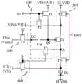
本申请提供一种像素驱动电路,包括:发光器件D1,驱动晶体管Td,补偿模块100及数据写入模块200;所述驱动晶体管Td用于为所述发光器件D1提供驱动电流;所述补偿模块100至少包括:The present application provides a pixel driving circuit, comprising: a light-emitting device D1, a driving transistor Td, a
存储电容Cst,所述存储电容Cst用于维持所述驱动晶体管Td的栅极电压;a storage capacitor Cst, the storage capacitor Cst is used to maintain the gate voltage of the driving transistor Td;
第一晶体管T1,所述第一晶体管T1的源极或漏极中的一者与所述驱动晶体管Td的栅极连接,所述第一晶体管T1用于将第一复位信号VI1传输至所述驱动晶体管Td的所述栅极;A first transistor T1, one of the source or drain of the first transistor T1 is connected to the gate of the driving transistor Td, and the first transistor T1 is used to transmit the first reset signal VI1 to the the gate of the drive transistor Td;
第二晶体管T2,所述第二晶体管T2用于将第二复位信号VI2传输至所述驱动晶体管Td的源极或漏极中的一者;a second transistor T2, the second transistor T2 is used for transmitting the second reset signal VI2 to one of the source or the drain of the driving transistor Td;
补偿晶体管T3,所述存储电容Cst串联在所述补偿晶体管T3的源极或漏极中的一者与所述驱动晶体管Td的所述栅极之间,所述补偿晶体管T3的所述源极或所述漏极中的另一者与所述驱动晶体管Td的所述源极或所述漏极中的一者连接,所述补偿晶体管T3用于与所述第二晶体管T2、所述存储电容Cst补偿所述驱动晶体管Td的阈值电压Vth;Compensation transistor T3, the storage capacitor Cst is connected in series between one of the source or drain of the compensation transistor T3 and the gate of the drive transistor Td, the source of the compensation transistor T3 or the other one of the drains is connected to one of the source or the drain of the drive transistor Td, the compensation transistor T3 is used for connecting with the second transistor T2, the storage The capacitor Cst compensates the threshold voltage Vth of the driving transistor Td;
所述数据写入模块200至少包括:数据写入晶体管T4,所述数据写入晶体管T4的源极或漏极中的一者与所述存储电容Cst的上极板连接,所述数据写入晶体管T4用于将数据信号Vdata写入所述存储电容Cst,并将所述数据信号Vdata传输至所述驱动晶体管Td的所述栅极。The
所述像素驱动电路通过所述补偿模块100中的所述第一晶体管T1实现对所述驱动晶体管Td栅极电压的复位,通过所述补偿模块100中的所述第二晶体管T2、所述补偿晶体管T3及所述存储电容Cst实现对所述驱动晶体管Td阈值电压Vth的采样及补偿,以改善显示效果,并降低功耗。The pixel driving circuit realizes the reset of the gate voltage of the driving transistor Td through the first transistor T1 in the
请继续参阅图2A~图2F,所述驱动晶体管Td与所述第一晶体管T1、所述第二晶体管T2、所述补偿晶体管T3及所述数据写入晶体管T4的类型不同。Please continue to refer to FIGS. 2A to 2F , the driving transistor Td is of a different type from the first transistor T1 , the second transistor T2 , the compensation transistor T3 and the data writing transistor T4 .
具体地,所述驱动晶体管Td为硅晶体管,所述第一晶体管T1、所述第二晶体管T2、所述补偿晶体管T3及所述数据写入晶体管T4为氧化物晶体管,以利用氧化物晶体管的漏电流小于硅晶体管的漏电流的特性,降低所述驱动晶体管Td的源极或漏极(A点)中的一者对所述驱动晶体管Td栅极(Q1点)电压的影响,从而保证所述驱动晶体管Td的栅极电压稳定。Specifically, the driving transistor Td is a silicon transistor, the first transistor T1 , the second transistor T2 , the compensation transistor T3 and the data writing transistor T4 are oxide transistors, so as to utilize the power of the oxide transistors. The characteristic that the leakage current is smaller than that of the silicon transistor reduces the influence of one of the source or drain (point A) of the driving transistor Td on the voltage of the gate (point Q1) of the driving transistor Td, thereby ensuring that all The gate voltage of the driving transistor Td is stabilized.
其中,所述硅晶体管包括单晶硅晶体管、多晶硅晶体管、微晶硅晶体管、非晶硅或其他含硅的晶体管;所述氧化物晶体管包括含锌、铟、镓、锡或钛等金属及其氧化物的氧化物晶体管。进一步地,所述多晶硅晶体管包括低温多晶硅晶体管;所述氧化物晶体管包括含氧化锌、氧化锌锡、氧化锌铟、氧化铟、氧化钛、氧化铟镓锌、氧化铟锌锡等的氧化物晶体管。Wherein, the silicon transistors include monocrystalline silicon transistors, polycrystalline silicon transistors, microcrystalline silicon transistors, amorphous silicon or other transistors containing silicon; the oxide transistors include metals such as zinc, indium, gallium, tin or titanium, and the like. oxide transistors. Further, the polysilicon transistors include low temperature polysilicon transistors; the oxide transistors include oxide transistors containing zinc oxide, zinc tin oxide, zinc indium oxide, indium oxide, titanium oxide, indium gallium zinc oxide, indium zinc tin oxide, etc. .
所述驱动晶体管Td可以为P型晶体管或N型晶体管;所述第一晶体管T1、所述第二晶体管T2、所述补偿晶体管T3及所述数据写入晶体管T4可以为P型晶体管或N型晶体管。进一步地,所述驱动晶体管Td为P型晶体管;所述第一晶体管T1、所述第二晶体管T2、所述补偿晶体管T3及所述数据写入晶体管T4为N型晶体管。The driving transistor Td may be a P-type transistor or an N-type transistor; the first transistor T1, the second transistor T2, the compensation transistor T3 and the data writing transistor T4 may be a P-type transistor or an N-type transistor transistor. Further, the driving transistor Td is a P-type transistor; the first transistor T1 , the second transistor T2 , the compensation transistor T3 and the data writing transistor T4 are N-type transistors.
请继续参阅图1A~图1D及图2A~图2F,所述像素驱动电路还包括用于控制所述发光器件D1发光的发光控制模块300,所述发光控制模块300至少包括:Please continue to refer to FIGS. 1A-1D and 2A-2F, the pixel driving circuit further includes a light-
第一开关晶体管T5,所述第一开关晶体管T5的源极或漏极中的一者与第二电压端ELVDD连接,所述源极或所述漏极中的另一者与所述驱动晶体管Td的所述源极或所述漏极中的一者连接;a first switching transistor T5, one of the source or the drain of the first switching transistor T5 is connected to the second voltage terminal ELVDD, and the other of the source or the drain is connected to the driving transistor one of the source or the drain of Td is connected;
第二开关晶体管T6,所述第二开关晶体管T6的源极或漏极中的一者与所述驱动晶体管Td的所述源极或所述漏极中的一者连接,所述源极或所述漏极中的另一者与所述发光器件D1的阳极连接。A second switching transistor T6, one of the source or the drain of the second switching transistor T6 is connected to one of the source or the drain of the driving transistor Td, the source or The other of the drains is connected to the anode of the light emitting device D1.
进一步地,所述第一开关晶体管T5及所述第二开关晶体管T6与所述驱动晶体管Td的类型相同;具体地,所述第一开关晶体管T5及所述第二开关晶体管T6为硅晶体管。所述第一开关晶体管T5及所述第二开关晶体管T6可以为P型晶体管,也可为N型晶体管,在此对其不再进行赘述。Further, the first switching transistor T5 and the second switching transistor T6 are of the same type as the driving transistor Td; specifically, the first switching transistor T5 and the second switching transistor T6 are silicon transistors. The first switching transistor T5 and the second switching transistor T6 may be either P-type transistors or N-type transistors, which will not be described herein again.
请继续参阅图1A~图1B、图2A~图2B及图3A,所述第一开关晶体管T5的栅极与第一发光控制信号线EM11连接,所述第二开关晶体管T6的栅极与第二发光控制信号线EM12连接,所述第二晶体管T2的源极或漏极中的一者与所述第二开关晶体管T6的所述源极或所述漏极中的一者连接,所述第二晶体管T2用于将所述第二复位信号VI2传输至所述发光器件D1的所述阳极,初始化所述发光器件D1的阳极电压。Please continue to refer to FIGS. 1A-1B, 2A-2B and 3A, the gate of the first switching transistor T5 is connected to the first light-emitting control signal line EM11, and the gate of the second switching transistor T6 is connected to the first light-emitting control signal line EM11. Two light-emitting control signal lines EM12 are connected, one of the source or the drain of the second transistor T2 is connected to one of the source or the drain of the second switching transistor T6, the The second transistor T2 is used to transmit the second reset signal VI2 to the anode of the light emitting device D1 to initialize the anode voltage of the light emitting device D1.
进一步地,所述第二发光控制信号线EM12载入的第二发光控制信号EM(n+1)滞后所述第一发光控制信号线EM11载入的第一发光控制信号EM(n),所述第一复位信号VI1与所述第二复位信号VI2的电压值相等,以使所述第二晶体管T2与所述第二开关晶体管T6同时导通时,实现对所述驱动晶体管Td阈值电压Vth的补偿及所述发光器件D1阳极的复位。Further, the second light-emitting control signal EM(n+1) carried by the second light-emitting control signal line EM12 lags the first light-emitting control signal EM(n) carried by the first light-emitting control signal line EM11, so The voltage values of the first reset signal VI1 and the second reset signal VI2 are equal, so that when the second transistor T2 and the second switching transistor T6 are turned on at the same time, the threshold voltage Vth of the driving transistor Td can be controlled. compensation and reset of the anode of the light-emitting device D1.
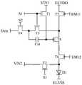
请继续参阅图1C~图1D、图2C~图2F及图3B,所述第二晶体管T2的所述源极或所述漏极中的一者与所述驱动晶体管Td的所述源极或所述漏极中的一者连接。Please continue to refer to FIGS. 1C to 1D , 2C to 2F and 3B, one of the source or the drain of the second transistor T2 and the source or the drain of the driving transistor Td One of the drains is connected.
进一步地,所述像素驱动电路还包括复位模块400,所述复位模块400至少包括:复位晶体管T7,所述复位晶体管T7的源极或漏极中的一者与所述发光器件D1的阳极连接,所述复位晶体管T7用于将所述第一复位信号VI1传输至所述发光器件D1的阳极,以实现对所述发光器件D1的阳极电压的复位。进一步地,所述复位晶体管T7与所述第一开关晶体管T5、所述第二开关晶体管T6及所述驱动晶体管Td的类型不同;更进一步地,所述复位晶体管T7为氧化物晶体管。Further, the pixel driving circuit further includes a
进一步地,所述复位晶体管T7的半导体层中的载流子与所述第一开关晶体管T5、所述第二开关晶体管T6的半导体层中的载流子的类型不同;具体地,所述复位晶体管T7为N型晶体管或P型晶体管的其中之一,所述第一开关晶体管T5、所述第二开关晶体管T6为N型晶体管或P型晶体管的其中另一。更进一步地,所述复位晶体管T7为N型晶体管,所述第一开关晶体管T5和所述第二开关晶体管T6为P型晶体管。Further, the type of carriers in the semiconductor layer of the reset transistor T7 is different from the type of carriers in the semiconductor layers of the first switching transistor T5 and the second switching transistor T6; The transistor T7 is one of an N-type transistor or a P-type transistor, and the first switching transistor T5 and the second switching transistor T6 are the other of the N-type transistor or the P-type transistor. Further, the reset transistor T7 is an N-type transistor, and the first switch transistor T5 and the second switch transistor T6 are P-type transistors.
所述第一晶体管T1的栅极、所述第二晶体管T2的栅极、所述补偿晶体管T3的栅极及所述复位晶体管T7的栅极可以与第一扫描信号线S1连接,利用所述第一扫描信号线S1载入的第一扫描信号Nscan(n-1)实现对所述第一晶体管T1、所述第二晶体管T2、所述补偿晶体管T3及所述复位晶体管T7控制,可以降低控制信号线的数量。The gate of the first transistor T1, the gate of the second transistor T2, the gate of the compensation transistor T3 and the gate of the reset transistor T7 may be connected to the first scan signal line S1, and the The first scan signal Nscan(n-1) carried by the first scan signal line S1 controls the first transistor T1, the second transistor T2, the compensation transistor T3 and the reset transistor T7, which can reduce the Controls the number of signal lines.
此外,所述复位晶体管T7还可与所述第一开关晶体管T5和所述第二开关晶体管T6共用同一控制信号线;具体地,所述复位晶体管T7的栅极、所述第一开关晶体管T5的栅极及所述第二开关晶体管T6的栅极与发光控制信号线EM1连接,利用所述发光控制信号线EM1载入的发光控制信号EM实现对所述第一开关晶体管T5、所述第二开关晶体管T6及所述复位晶体管T7的控制,以降低控制信号线的数量。In addition, the reset transistor T7 may also share the same control signal line with the first switch transistor T5 and the second switch transistor T6; specifically, the gate of the reset transistor T7, the first switch transistor T5 The gate of the second switching transistor T6 and the gate of the second switching transistor T6 are connected to the light-emitting control signal line EM1, and the light-emitting control signal EM loaded by the light-emitting control signal line EM1 is used to realize the control of the first switching transistor T5, the The two switch transistors T6 and the reset transistor T7 are controlled to reduce the number of control signal lines.
由于所述复位晶体管T7为N型晶体管或P型晶体管的其中之一,所述第一开关晶体管T5、所述第二开关晶体管T6为N型晶体管或P型晶体管的其中另一,所以,在利用所述发光控制信号EM对所述发光器件D1的阳极进行复位时,所述第一开关晶体管T5、所述第二开关晶体管T6均处于截止状态,可增加对所述发光器件D1阳极的复位时长,也不会影响所述发光器件D1的正常显示。此外,还可单独设置控制信号以控制所述复位晶体管T7实现对所述发光器件D1阳极的复位,在此对其不再进行赘述。Since the reset transistor T7 is one of an N-type transistor or a P-type transistor, and the first switch transistor T5 and the second switch transistor T6 are the other of the N-type transistor or the P-type transistor, in When the anode of the light-emitting device D1 is reset by using the light-emitting control signal EM, the first switching transistor T5 and the second switching transistor T6 are both in an off state, which can increase the reset of the anode of the light-emitting device D1 The time duration will not affect the normal display of the light-emitting device D1. In addition, a control signal can also be set separately to control the reset transistor T7 to reset the anode of the light-emitting device D1, which will not be repeated here.
请继续参阅图1C~图1D、图2C~图2F及图3B,所述第一复位信号VI1与所述第二复位信号VI2为直流低电平信号,且所述第一复位信号VI1的电压值与所述第二复位信号VI2的电压值不同。进一步地,所述第一复位信号VI1的电压值小于所述第二复位信号VI2的电压值,以使所述存储电容Cst可以通过所述补偿晶体管T3、所述第二晶体管T2向载入所述第二复位信号VI2的第二复位信号线VIN2放电,从而使所述存储电容Cst对所述驱动晶体管Td的阈值电压Vth进行采样,实现对所述驱动晶体管Td的阈值电压Vth的补偿。Please continue to refer to FIGS. 1C to 1D , 2C to 2F and 3B. The first reset signal VI1 and the second reset signal VI2 are DC low level signals, and the voltage of the first reset signal VI1 The value is different from the voltage value of the second reset signal VI2. Further, the voltage value of the first reset signal VI1 is smaller than the voltage value of the second reset signal VI2, so that the storage capacitor Cst can be loaded to the load through the compensation transistor T3 and the second transistor T2. The second reset signal line VIN2 of the second reset signal VI2 is discharged, so that the storage capacitor Cst samples the threshold voltage Vth of the driving transistor Td to compensate the threshold voltage Vth of the driving transistor Td.
可以理解的,由于所述第一复位信号VI1与所述第二复位信号VI2为直流低电平信号,所以,所述第一复位信号VI1的电压值小于所述第二复位信号VI2的电压值是指在所述第一复位信号VI1的电压值取负值时,所述第二复位信号VI2的电压值取比所述第一复位信号VI1的电压值更负的负值。It can be understood that since the first reset signal VI1 and the second reset signal VI2 are DC low level signals, the voltage value of the first reset signal VI1 is smaller than the voltage value of the second reset signal VI2 It means that when the voltage value of the first reset signal VI1 takes a negative value, the voltage value of the second reset signal VI2 takes a negative value that is more negative than the voltage value of the first reset signal VI1.
与之相似的,所述第一复位信号VI1与所述第二复位信号VI2还可为直流高电平信号;进一步地,所述第一复位信号VI1的电压值大于所述第二复位信号VI2的电压值;即若所述第一复位信号VI1的电压值取正值时,所述第二复位信号VI2的电压值取比所述第一复位信号VI1的电压值小的正值。Similarly, the first reset signal VI1 and the second reset signal VI2 may also be DC high level signals; further, the voltage value of the first reset signal VI1 is greater than that of the second reset signal VI2 That is, if the voltage value of the first reset signal VI1 takes a positive value, the voltage value of the second reset signal VI2 takes a positive value smaller than the voltage value of the first reset signal VI1.
请继续参阅图1A~图1D及图2A~图2F,所述数据写入晶体管T4的栅极与第二扫描信号线S2连接,以响应所述第二扫描信号线S2载入的第二扫描信号Nscan(n),将所述数据信号Vdata写入所述存储电容Cst中,并传输至所述驱动晶体管Td的栅极。Please continue to refer to FIGS. 1A to 1D and FIGS. 2A to 2F , the gate of the data writing transistor T4 is connected to the second scan signal line S2 in response to the second scan loaded by the second scan signal line S2 The signal Nscan(n) writes the data signal Vdata into the storage capacitor Cst and transmits it to the gate of the driving transistor Td.
所述发光器件D1的阴极与第一电压端ELVSS连接,所述发光器件D1包括有机发光二极管、次毫米发光二极管及微型发光二极管的其中一种。The cathode of the light-emitting device D1 is connected to the first voltage terminal ELVSS, and the light-emitting device D1 includes one of an organic light-emitting diode, a sub-millimeter light-emitting diode and a micro light-emitting diode.
所述驱动晶体管Td的栅极可以共用作所述存储电容Cst的下极板,以实现最优的空间分配,并节省制程工序。此外,所述存储电容Cst的下极板亦可单独形成,在此对其不再进行赘述。The gates of the driving transistors Td can be jointly used as the lower plate of the storage capacitor Cst, so as to achieve optimal space allocation and save process steps. In addition, the lower plate of the storage capacitor Cst can also be formed separately, which will not be repeated here.
在图1A~图1D及图2A~图2F所示的像素驱动电路中,均以所述发光器件D1的阴极接第一电压端ELVSS为例;此外,所述发光器件D1亦可采用阳极接所述第二电压端ELVDD的形式布置于所述像素驱动电路中,在此对其不再进行赘述。In the pixel driving circuits shown in FIGS. 1A to 1D and FIGS. 2A to 2F , the cathode of the light-emitting device D1 is connected to the first voltage terminal ELVSS as an example; in addition, the light-emitting device D1 can also be connected to the anode. The form of the second voltage terminal ELVDD is arranged in the pixel driving circuit, which will not be repeated here.
本申请还提供一种像素驱动电路的驱动方法,用于驱动所述的像素驱动电路,在第N帧周期内,所述驱动方法包括:The present application also provides a driving method for a pixel driving circuit, which is used for driving the pixel driving circuit. During the Nth frame period, the driving method includes:
初始化阶段t1,所述补偿模块100的所述第一晶体管T1将所述第一复位信号VI1传输至所述驱动晶体管Td的所述栅极,初始化所述驱动晶体管Td的栅极电压(即所述第一复位信号VI1传输至Q1点),所述第二晶体管T2、所述补偿晶体管T3及所述存储电容Cst补偿所述驱动晶体管Td的阈值电压Vth;In the initialization stage t1, the first transistor T1 of the
数据写入阶段t2,所述存储电容Cst写入所述数据信号Vdata,并将所述数据信号Vdata传输至所述驱动晶体管Td的所述栅极;In the data writing stage t2, the storage capacitor Cst writes the data signal Vdata, and transmits the data signal Vdata to the gate of the driving transistor Td;
发光阶段t3,所述驱动晶体管Td驱动发光器件D1发光,所述补偿模块100补偿所述驱动晶体管Td的阈值电压Vth。In the light-emitting stage t3, the driving transistor Td drives the light-emitting device D1 to emit light, and the
下面将结合图2A~图2F及图3A~图3C详细描述利用所述驱动方法驱动所述像素驱动电路的工作原理。其中,在图2A~图2F所示的像素驱动电路中,均以所述驱动晶体管Td、所述第一开关晶体管T5及所述第二开关晶体管T6为P型硅晶体管,所述第一晶体管T1、所述第二晶体管T2、所述补偿晶体管T3、所述数据写入晶体管T4为N型氧化物晶体管为例,在图2C~图2F所示的像素驱动电路中以所述复位晶体管T7为N型氧化物晶体管进行说明。The working principle of driving the pixel driving circuit by using the driving method will be described in detail below with reference to FIGS. 2A to 2F and FIGS. 3A to 3C . Wherein, in the pixel driving circuits shown in FIGS. 2A to 2F , the driving transistor Td, the first switching transistor T5 and the second switching transistor T6 are all P-type silicon transistors, and the first transistor T1, the second transistor T2, the compensation transistor T3, and the data writing transistor T4 are N-type oxide transistors as an example, in the pixel driving circuit shown in FIG. 2C to FIG. 2F, the reset transistor T7 is used as an example. An N-type oxide transistor will be described.
具体地,请继续参阅图2A~图2B及图3A,以所述第一复位信号VI1与所述第二复位信号VI2的电压值相等为例,在第N帧周期内包括:Specifically, please continue to refer to FIGS. 2A to 2B and FIG. 3A. Taking the voltage values of the first reset signal VI1 and the second reset signal VI2 being equal as an example, the Nth frame period includes:
在所述初始化阶段t1:所述第一晶体管T1、所述第二晶体管T2、所述补偿晶体管T3响应所述第一扫描信号线S1载入的第一扫描信号Nscan(n-1)导通,所述第二开关晶体管T6响应所述第二发光控制信号线EM12载入的第二发光控制信号EM(n+1)导通,所述第一复位信号线VIN1载入的所述第一复位信号VI1被传输至所述驱动晶体管Td的栅极,所述第二复位信号线VIN2载入的所述第二复位信号VI2传输至所述发光器件D1的阳极,初始化所述驱动晶体管Td的栅极电压(即所述第一复位信号VI1传输至Q1点)及所述发光器件D1的阳极电压;与此同时,由于所述第二晶体管T2、所述补偿晶体管T3导通,所述存储电容Cst放电(即在图2A中从Q2点经所述补偿晶体管T3、所述驱动晶体管Td及所述第二晶体管T2向所述第二复位信号线VIN2放电;在图2B中从Q2点经所述补偿晶体管T3、所述驱动晶体管Td、所述第二开关晶体管T6及所述第二晶体管T2向所述第二复位信号线VIN2放电),直至A点电压等于所述驱动晶体管Td的栅极电压(即Q1点处的电压)与所述驱动晶体管Td的阈值电压Vth之和,所述驱动晶体管Td截止,所述补偿晶体管T3导通使得A点的电压等于Q2点的电压,即所述存储电容Cst上极板与下极板之间的电压差等于所述驱动晶体管Td的阈值电压Vth,从而实现对所述驱动晶体管Td的阈值电压Vth的采样及补偿。In the initialization stage t1: the first transistor T1, the second transistor T2, and the compensation transistor T3 are turned on in response to the first scan signal Nscan(n-1) loaded by the first scan signal line S1 , the second switching transistor T6 is turned on in response to the second light-emitting control signal EM(n+1) loaded by the second light-emitting control signal line EM12, and the first reset signal line VIN1 The reset signal VI1 is transmitted to the gate of the driving transistor Td, the second reset signal VI2 carried by the second reset signal line VIN2 is transmitted to the anode of the light-emitting device D1, and the driving transistor Td is initialized. The gate voltage (that is, the first reset signal VI1 is transmitted to the Q1 point) and the anode voltage of the light-emitting device D1; at the same time, since the second transistor T2 and the compensation transistor T3 are turned on, the storage The capacitor Cst is discharged (that is, in FIG. 2A, it is discharged to the second reset signal line VIN2 from the point Q2 through the compensation transistor T3, the driving transistor Td and the second transistor T2; in FIG. The compensation transistor T3, the driving transistor Td, the second switching transistor T6 and the second transistor T2 discharge to the second reset signal line VIN2) until the voltage at point A is equal to the gate of the driving transistor Td The sum of the pole voltage (ie the voltage at point Q1) and the threshold voltage Vth of the driving transistor Td, the driving transistor Td is turned off, and the compensation transistor T3 is turned on so that the voltage at point A is equal to the voltage at point Q2, that is, the The voltage difference between the upper plate and the lower plate of the storage capacitor Cst is equal to the threshold voltage Vth of the driving transistor Td, thereby realizing sampling and compensation of the threshold voltage Vth of the driving transistor Td.
在所述数据写入阶段t2:所述数据写入晶体管T4响应所述第二扫描信号线S2载入的所述第二扫描信号Nscan(n)导通,所述存储电容Cst的上极板(即Q2点)写入所述数据信号线Data载入的所述数据信号Vdata,并将所述数据信号Vdata传输至所述驱动晶体管Td的栅极(即Q1点),完成所述数据信号Vdata的写入。In the data writing stage t2: the data writing transistor T4 is turned on in response to the second scan signal Nscan(n) loaded by the second scan signal line S2, and the upper plate of the storage capacitor Cst is turned on. (ie Q2 point) write the data signal Vdata loaded by the data signal line Data, and transmit the data signal Vdata to the gate of the driving transistor Td (ie Q1 point), complete the data signal Write of Vdata.
在所述发光阶段t3:所述第一开关晶体管T5响应所述第一发光控制信号线EM11载入的所述第一发光控制信号EM(n)导通,所述第二开关晶体管T6响应所述第二发光控制信号线EM12载入的所述第二发光控制信号EM(n+1)导通;若在所述数据写入阶段t2传输至所述驱动晶体管Td的栅极的所述数据信号Vdata可以使所述驱动晶体管Td导通,则所述驱动晶体管Td由于所述第一开关晶体管T5及所述第二开关晶体管T6的导通产生驱动电流驱动所述发光器件D1发光;若在所述数据写入阶段t2传输至所述驱动晶体管Td的栅极的所述数据信号Vdata不能使所述驱动晶体管Td导通,则所述驱动晶体管Td仍保持截止状态,即使所述第一开关晶体管T5及所述第二开关晶体管T6的导通,所述发光器件D1也不发光。In the light-emitting stage t3: the first switch transistor T5 is turned on in response to the first light-emitting control signal EM(n) carried by the first light-emitting control signal line EM11, and the second switch transistor T6 is turned on in response to the first light-emitting control signal line EM11. The second light-emitting control signal EM(n+1) carried by the second light-emitting control signal line EM12 is turned on; if the data transmitted to the gate of the driving transistor Td in the data writing phase t2 The signal Vdata can turn on the driving transistor Td, then the driving transistor Td generates a driving current to drive the light-emitting device D1 to emit light due to the turn-on of the first switching transistor T5 and the second switching transistor T6; If the data signal Vdata transmitted to the gate of the driving transistor Td in the data writing phase t2 cannot turn the driving transistor Td on, the driving transistor Td remains in an off state even if the first switch When the transistor T5 and the second switching transistor T6 are turned on, the light-emitting device D1 does not emit light.
由于在所述初始化阶段t1中,所述第二晶体管T2与所述第二开关晶体管T6同时导通,因此,在图2A中可利用所述第二晶体管T2与所述第二开关晶体管T6实现对所述发光器件D1的阳极的复位,通过所述第二晶体管T2与所述补偿晶体管T3、所述存储电容Cst补偿所述驱动晶体管Td的阈值电压Vth;在图2B中可利用所述第二晶体管T2实现对所述发光器件D1的阳极的复位,所述第二晶体管T2可间接的通过所述第二开关晶体管T6与所述补偿晶体管T3及所述存储电容Cst实现对所述驱动晶体管Td阈值电压的补偿;从而可以省略设置对所述发光器件D1的阳极复位的晶体管。Since in the initialization phase t1, the second transistor T2 and the second switch transistor T6 are turned on at the same time, therefore, in FIG. 2A, the second transistor T2 and the second switch transistor T6 can be used to realize For resetting the anode of the light-emitting device D1, the threshold voltage Vth of the driving transistor Td is compensated by the second transistor T2, the compensation transistor T3, and the storage capacitor Cst; in FIG. 2B, the first Two transistors T2 realize the reset of the anode of the light-emitting device D1, and the second transistor T2 can realize the drive transistor indirectly through the second switch transistor T6, the compensation transistor T3 and the storage capacitor Cst. Compensation of the Td threshold voltage; thus the transistor provided to reset the anode of the light emitting device D1 can be omitted.
此外,也可单独设置对所述发光器件D1的阳极进行复位的晶体管,具体地,请继续参阅图2C~图2F及图3B~图3C,以所述第一复位信号VI1与所述第二复位信号VI2为低电平信号,且所述第一复位信号VI1的电压值小于所述第二复位信号VI2的电压值为例进行说明。In addition, a transistor for resetting the anode of the light-emitting device D1 can also be provided separately. Specifically, please continue to refer to FIGS. 2C to 2F and 3B to 3C, using the first reset signal VI1 and the second reset signal VI1 and the second The reset signal VI2 is a low level signal, and the voltage value of the first reset signal VI1 is lower than the voltage value of the second reset signal VI2 as an example for description.
请继续参阅图2C~图2D及图3B~图3C,以所述复位晶体管T7与所述第一晶体管T1、所述第二晶体管T2及所述补偿晶体管T3共用第一扫描信号Nscan(n-1)为例,在第N帧周期内包括:Please continue to refer to FIGS. 2C to 2D and 3B to 3C. The reset transistor T7 shares the first scan signal Nscan (n- 1) For example, the Nth frame period includes:
在所述初始化阶段t1:所述第一晶体管T1、所述第二晶体管T2、所述补偿晶体管T3及所述复位晶体管T7响应所述第一扫描信号线S1载入的所述第一扫描信号Nscan(n-1)导通,所述第一复位信号线VIN1载入的所述第一复位信号VI1被传输至所述驱动晶体管Td的栅极和所述发光器件D1的阳极,初始化所述驱动晶体管Td的栅极电压及所述发光器件D1的阳极电压;与此同时,由于所述第二晶体管T2、所述补偿晶体管T3导通,所述第二复位信号VI2的电压值较所述第一复位信号VI1的电压值更负,所以所述存储电容Cst从Q2点经所述补偿晶体管T3、所述驱动晶体管Td及所述第二晶体管T2向所述第二复位信号线VIN2放电,直至A点电压等于所述驱动晶体管Td的栅极电压(即Q1点处的电压)与所述驱动晶体管Td的阈值电压Vth之和,所述驱动晶体管Td截止,所述补偿晶体管T3导通使得A点的电压等于Q2点的电压,即所述存储电容Cst上极板与下极板之间的电压差等于所述驱动晶体管Td的阈值电压Vth,从而实现对所述驱动晶体管Td的阈值电压Vth的采样及补偿。In the initialization phase t1: the first transistor T1, the second transistor T2, the compensation transistor T3 and the reset transistor T7 respond to the first scan signal loaded by the first scan signal line S1 Nscan(n-1) is turned on, the first reset signal VI1 carried by the first reset signal line VIN1 is transmitted to the gate of the driving transistor Td and the anode of the light-emitting device D1, and the The gate voltage of the driving transistor Td and the anode voltage of the light-emitting device D1; at the same time, since the second transistor T2 and the compensation transistor T3 are turned on, the voltage value of the second reset signal VI2 is higher than that of the second reset signal VI2. The voltage value of the first reset signal VI1 is more negative, so the storage capacitor Cst is discharged from the point Q2 to the second reset signal line VIN2 through the compensation transistor T3, the driving transistor Td and the second transistor T2, Until the voltage at point A is equal to the sum of the gate voltage of the driving transistor Td (ie the voltage at point Q1) and the threshold voltage Vth of the driving transistor Td, the driving transistor Td is turned off, and the compensation transistor T3 is turned on so that The voltage of point A is equal to the voltage of point Q2, that is, the voltage difference between the upper plate and the lower plate of the storage capacitor Cst is equal to the threshold voltage Vth of the driving transistor Td, so as to realize the threshold voltage of the driving transistor Td Sampling and compensation of Vth.
在所述数据写入阶段t2:所述数据写入晶体管T4响应所述第二扫描信号线S2载入的所述第二扫描信号Nscan(n)导通,所述存储电容Cst的上极板(即Q2点)写入所述数据信号线Data载入的所述数据信号Vdata,并将所述数据信号Vdata传输至所述驱动晶体管Td的栅极(即Q1点),完成所述数据信号Vdata的写入。In the data writing stage t2: the data writing transistor T4 is turned on in response to the second scan signal Nscan(n) loaded by the second scan signal line S2, and the upper plate of the storage capacitor Cst is turned on. (ie Q2 point) write the data signal Vdata loaded by the data signal line Data, and transmit the data signal Vdata to the gate of the driving transistor Td (ie Q1 point), complete the data signal Write of Vdata.
在所述发光阶段t3:所述第一开关晶体管T5及所述第二开关晶体管T6响应所述发光控制信号线EM1载入的所述发光控制信号EM,若在所述数据写入阶段t2传输至所述驱动晶体管Td的栅极的所述数据信号Vdata可以使所述驱动晶体管Td导通,则所述驱动晶体管Td由于所述第一开关晶体管T5及所述第二开关晶体管T6的导通产生驱动电流驱动所述发光器件D1发光;若在所述数据写入阶段t2传输至所述驱动晶体管Td的栅极的所述数据信号Vdata不能使所述驱动晶体管Td导通,则所述驱动晶体管Td仍保持截止状态,即使所述第一开关晶体管T5及所述第二开关晶体管T6的导通,所述发光器件D1也不发光。In the light-emitting phase t3: the first switch transistor T5 and the second switch transistor T6 respond to the light-emitting control signal EM loaded from the light-emitting control signal line EM1, if the first switch transistor T5 and the second switch transistor T6 transmit the light-emitting control signal EM in the data writing phase t2 The data signal Vdata to the gate of the driving transistor Td can turn on the driving transistor Td, then the driving transistor Td is turned on due to the conduction of the first switching transistor T5 and the second switching transistor T6 A driving current is generated to drive the light-emitting device D1 to emit light; if the data signal Vdata transmitted to the gate of the driving transistor Td in the data writing phase t2 cannot turn on the driving transistor Td, the driving The transistor Td remains in an off state, and even if the first switching transistor T5 and the second switching transistor T6 are turned on, the light-emitting device D1 does not emit light.
与之相似的,请继续参阅图2E~图2F及图3B~图3C,以所述复位晶体管T7与所述第一开关晶体管T5、所述第二开关晶体管T6共用发光控制信号EM为例,在第N帧周期内包括:Similarly, please continue to refer to FIGS. 2E to 2F and FIGS. 3B to 3C. Taking the reset transistor T7, the first switch transistor T5 and the second switch transistor T6 sharing the light-emitting control signal EM as an example, In the Nth frame period includes:
在所述初始化阶段t1:所述第一晶体管T1、所述第二晶体管T2及所述补偿晶体管T3响应所述第一扫描信号Nscan(n-1)导通;所述复位晶体管T7响应所述发光控制信号EM导通,所述第一复位信号VI1被传输至所述驱动晶体管Td的栅极及所述发光器件D1的阳极,初始化所述驱动晶体管Td的栅极电压及所述发光器件D1的阳极电压;与此同时,所述存储电容Cst从Q2点经所述补偿晶体管T3、所述驱动晶体管Td及所述第二晶体管T2向所述第二复位信号线VIN2放电,直至A点电压等于所述驱动晶体管Td的栅极电压(即Q1点处的电压)与所述驱动晶体管Td的阈值电压Vth之和,所述驱动晶体管Td截止,所述存储电容Cst上极板与下极板之间的电压差等于所述驱动晶体管Td的阈值电压Vth,从而实现对所述驱动晶体管Td的阈值电压Vth的采样及补偿。In the initialization phase t1: the first transistor T1, the second transistor T2 and the compensation transistor T3 are turned on in response to the first scan signal Nscan(n-1); the reset transistor T7 is turned on in response to the The light-emitting control signal EM is turned on, the first reset signal VI1 is transmitted to the gate of the driving transistor Td and the anode of the light-emitting device D1, and the gate voltage of the driving transistor Td and the light-emitting device D1 are initialized At the same time, the storage capacitor Cst discharges from point Q2 to the second reset signal line VIN2 through the compensation transistor T3, the driving transistor Td and the second transistor T2 until the voltage at point A is reached is equal to the sum of the gate voltage of the drive transistor Td (ie the voltage at point Q1) and the threshold voltage Vth of the drive transistor Td, the drive transistor Td is turned off, and the upper and lower plates of the storage capacitor Cst The voltage difference between them is equal to the threshold voltage Vth of the driving transistor Td, so as to realize sampling and compensation of the threshold voltage Vth of the driving transistor Td.
在所述数据写入阶段t2:所述复位晶体管T7继续响应所述发光控制信号线EM1载入的所述发光控制信号EM导通,所述数据写入晶体管T4响应所述第二扫描信号线S2载入的所述第二扫描信号Nscan(n)导通;所述第一复位信号VI1被传输至所述发光器件D1的阳极,初始化所述发光器件D1的阳极电压;所述存储电容Cst的上极板(即Q2点)写入所述数据信号线Data载入的所述数据信号Vdata,并将所述数据信号Vdata传输至所述驱动晶体管Td的栅极(即Q1点),完成所述数据信号Vdata的写入。In the data writing phase t2: the reset transistor T7 continues to be turned on in response to the light emitting control signal EM loaded by the light emitting control signal line EM1, and the data writing transistor T4 responds to the second scanning signal line The second scan signal Nscan(n) loaded by S2 is turned on; the first reset signal VI1 is transmitted to the anode of the light-emitting device D1 to initialize the anode voltage of the light-emitting device D1; the storage capacitor Cst The upper plate of the upper plate (ie point Q2) writes the data signal Vdata loaded by the data signal line Data, and transmits the data signal Vdata to the gate of the driving transistor Td (ie point Q1), complete writing of the data signal Vdata.
在所述发光阶段t3:所述第一开关晶体管T5及所述第二开关晶体管T6响应所述发光控制信号线EM1载入的所述发光控制信号EM导通,所述复位晶体管T7响应所述发光控制信号线EM1载入的所述发光控制信号EM截止,若在所述数据写入阶段t2传输至所述驱动晶体管Td的栅极的所述数据信号Vdata可以使所述驱动晶体管Td导通,则所述驱动晶体管Td由于所述第一开关晶体管T5及所述第二开关晶体管T6的导通产生驱动电流驱动所述发光器件D1发光;若在所述数据写入阶段t2传输至所述驱动晶体管Td的栅极的所述数据信号Vdata不能使所述驱动晶体管Td导通,则所述驱动晶体管Td仍保持截止状态,即使所述第一开关晶体管T5及所述第二开关晶体管T6的导通,所述发光器件D1也不发光。In the light-emitting stage t3: the first switch transistor T5 and the second switch transistor T6 are turned on in response to the light-emitting control signal EM loaded from the light-emitting control signal line EM1, and the reset transistor T7 is turned on in response to the light-emitting control signal line EM1. The light-emitting control signal EM carried by the light-emitting control signal line EM1 is turned off, and the driving transistor Td can be turned on if the data signal Vdata transmitted to the gate of the driving transistor Td in the data writing phase t2 , the drive transistor Td drives the light-emitting device D1 to emit light due to the drive current generated by the conduction of the first switch transistor T5 and the second switch transistor T6; The data signal Vdata at the gate of the driving transistor Td cannot turn on the driving transistor Td, then the driving transistor Td remains in the off state, even if the first switching transistor T5 and the second switching transistor T6 are in the off state. When turned on, the light-emitting device D1 does not emit light.
在图2A~图2F中,由于在所述初始化阶段t1中所述补偿模块100对所述驱动晶体管Td的阈值电压Vth进行了采样及补偿,在所述数据写入阶段t2所述驱动晶体管Td的阈值电压Vth仍被储存在所述存储电容Cst中,所以在所述发光阶段t3,所述补偿模块100可以对所述驱动晶体管Td的阈值电压Vth进行补偿,从而消除阈值电压Vth的影响,保持所述发光器件D1发光的稳定性。In FIGS. 2A to 2F , since the
此外,由于所述第一晶体管T1、所述第二晶体管T2及所述补偿晶体管T3均为氧化物晶体管,具有较小的漏电流,因此可以降低所述驱动晶体管Td的源极或漏极(A点)中的一者对所述驱动晶体管Td栅极(Q1点)电压的影响,从而保证所述驱动晶体管Td的栅极电压稳定。In addition, since the first transistor T1, the second transistor T2 and the compensation transistor T3 are all oxide transistors and have a small leakage current, the source or drain ( A point) on the gate (Q1 point) voltage of the driving transistor Td, so as to ensure that the gate voltage of the driving transistor Td is stable.
通过图2C~图2F可知,所述复位晶体管T7与所述第一开关晶体管T5和所述第二开关晶体管T6共用所述发光控制信号EM,除可以减少控制信号线的数量外,还可以增加对所述发光器件D1的阳极复位的时长,保证所述发光器件D1的发光效果。It can be seen from FIG. 2C to FIG. 2F that the reset transistor T7 shares the light-emitting control signal EM with the first switching transistor T5 and the second switching transistor T6, which can not only reduce the number of control signal lines, but also increase the number of control signal lines. The duration of resetting the anode of the light-emitting device D1 ensures the light-emitting effect of the light-emitting device D1.
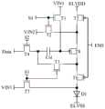
本申请还提供一种显示面板,包括像素驱动电路,如图4A~图4F所示,其为本申请的实施例提供的像素驱动电路的结构示意图,所述像素驱动电路包括:存储电容Cst,以及,The present application further provides a display panel including a pixel driving circuit, as shown in FIGS. 4A to 4F , which are schematic structural diagrams of the pixel driving circuit provided by the embodiments of the present application, and the pixel driving circuit includes: a storage capacitor Cst, as well as,
发光器件D1,所述发光器件D1的阴极与第一电压端ELVSS连接;a light-emitting device D1, the cathode of the light-emitting device D1 is connected to the first voltage terminal ELVSS;
第一晶体管T1,所述第一晶体管T1的栅极与第一扫描信号线S1连接,所述第一晶体管T1的源极或漏极中的一者与第一复位信号线VIN1连接,所述源极或所述漏极中的另一者与第八晶体管T8的栅极连接;The first transistor T1, the gate of the first transistor T1 is connected to the first scan signal line S1, the source or the drain of the first transistor T1 is connected to the first reset signal line VIN1, the the other of the source or the drain is connected to the gate of the eighth transistor T8;
第二晶体管T2,所述第二晶体管T2的栅极与所述第一扫描信号线S1连接,所述第二晶体管T2的源极或漏极中的一者与第二复位信号线VIN2连接;the second transistor T2, the gate of the second transistor T2 is connected to the first scan signal line S1, and one of the source or the drain of the second transistor T2 is connected to the second reset signal line VIN2;
第三晶体管T3,所述第三晶体管T3的栅极与所述第一扫描信号线S1连接,所述存储电容Cst串联在所述第三晶体管T3的源极或漏极中的一者与所述第八晶体管T8的栅极之间,所述第三晶体管T3的所述源极或所述漏极中的另一者与所述第八晶体管T8的源极或漏极中的一者连接;The third transistor T3, the gate of the third transistor T3 is connected to the first scan signal line S1, the storage capacitor Cst is connected in series with one of the source or drain of the third transistor T3 and the Between the gates of the eighth transistor T8, the other of the source or the drain of the third transistor T3 is connected to one of the source or the drain of the eighth transistor T8 ;
第四晶体管T4,所述第四晶体管T4的栅极与第二扫描信号线S2连接,所述第四晶体管T4的源极或漏极中的一者与数据信号线Data连接,所述源极或所述漏极中的另一者与所述存储电容Cst的上极板连接。The fourth transistor T4, the gate of the fourth transistor T4 is connected to the second scan signal line S2, the source or the drain of the fourth transistor T4 is connected to the data signal line Data, the source Or the other one of the drains is connected to the upper plate of the storage capacitor Cst.
其中,通过所述第一晶体管T1实现对所述第八晶体管T8栅极电压的复位,通过所述第二晶体管T2、所述第三晶体管T3及所述存储电容Cst实现对所述第八晶体管T8阈值电压Vth的采样及补偿,从而改善所述显示面板的显示效果,降低所述显示面板的功耗,有利于所述显示面板实现超低功耗显示。The gate voltage of the eighth transistor T8 is reset through the first transistor T1, and the eighth transistor is reset through the second transistor T2, the third transistor T3 and the storage capacitor Cst. Sampling and compensation of the T8 threshold voltage Vth, thereby improving the display effect of the display panel, reducing the power consumption of the display panel, and facilitating the display panel to realize ultra-low power consumption display.
在所述显示面板中,为优化空间分配并节省制程,所述第八晶体管T8的栅极可以共用作所述存储电容Cst的下极板。此外,所述存储电容Cst的下极板亦可单独制作,在此对其不再进行赘述。In the display panel, in order to optimize the space allocation and save the process, the gate of the eighth transistor T8 can be commonly used as the lower plate of the storage capacitor Cst. In addition, the lower plate of the storage capacitor Cst can also be fabricated separately, which will not be repeated here.
进一步地,所述第八晶体管T8与所述第一晶体管T1、所述第二晶体管T2、所述第三晶体管T3及所述第四晶体管T4具有不同材料的半导体层。Further, the eighth transistor T8 and the first transistor T1 , the second transistor T2 , the third transistor T3 and the fourth transistor T4 have semiconductor layers of different materials.
具体地,所述第八晶体管T8包括硅半导体层或氧化物半导体层的其中之一,所述第一晶体管T1、所述第二晶体管T2、所述第三晶体管T3及所述第四晶体管T4包括硅半导体层或氧化物半导体层的其中另一。进一步地,所述第八晶体管T8包括硅半导体层,所述第一晶体管T1、所述第二晶体管T2、所述第三晶体管T3及所述第四晶体管T4包括氧化物半导体层。Specifically, the eighth transistor T8 includes one of a silicon semiconductor layer or an oxide semiconductor layer, the first transistor T1 , the second transistor T2 , the third transistor T3 and the fourth transistor T4 The other of the silicon semiconductor layer or the oxide semiconductor layer is included. Further, the eighth transistor T8 includes a silicon semiconductor layer, and the first transistor T1 , the second transistor T2 , the third transistor T3 and the fourth transistor T4 include an oxide semiconductor layer.
其中,所述硅半导体层包括N型或者P型硅半导体;所述氧化物半导体层可包括氧化锌、氧化锌锡、氧化锌铟、氧化铟、氧化钛、氧化铟镓锌、氧化铟锌锡等中的至少一种。Wherein, the silicon semiconductor layer includes N-type or P-type silicon semiconductor; the oxide semiconductor layer may include zinc oxide, zinc tin oxide, zinc indium oxide, indium oxide, titanium oxide, indium gallium zinc oxide, indium zinc tin oxide at least one of etc.
请继续参阅图4A~图4F,所述像素驱动电路还包括:Please continue to refer to FIG. 4A to FIG. 4F , the pixel driving circuit further includes:
第五晶体管T5,所述第五晶体管T5的栅极与发光控制信号线EM1连接,所述第五晶体管T5的源极或漏极中的一者与第二电压端ELVDD连接,所述源极或所述漏极中的另一者与所述第八晶体管T8的源极或漏极中的一者连接;The fifth transistor T5, the gate of the fifth transistor T5 is connected to the light-emitting control signal line EM1, the source or the drain of the fifth transistor T5 is connected to the second voltage terminal ELVDD, the source or the other of the drains is connected to one of the source or the drain of the eighth transistor T8;
第六晶体管T6,所述第六晶体管T6的栅极与所述发光控制信号线EM1连接,所述第六晶体管T6的源极或漏极中的一者与所述第八晶体管T8的源极或漏极中的一者连接,源极或漏极中的另一者与发光器件D1的阳极连接。A sixth transistor T6, the gate of the sixth transistor T6 is connected to the light-emitting control signal line EM1, and one of the source or drain of the sixth transistor T6 is connected to the source of the eighth transistor T8 One of the drain or the drain is connected, and the other of the source or the drain is connected to the anode of the light emitting device D1.
进一步地,所述发光控制信号线EM1包括与所述第五晶体管T5的所述栅极连接的第一发光控制信号线EM11和与所述第六晶体管T6的所述栅极连接的第二发光控制信号线EM12;所述第二晶体管T2的所述源极或所述漏极中的一者与所述第六晶体管T6的源极或漏极中的一者连接。Further, the light emission control signal line EM1 includes a first light emission control signal line EM11 connected to the gate of the fifth transistor T5 and a second light emission control signal line connected to the gate of the sixth transistor T6 Control signal line EM12; one of the source or the drain of the second transistor T2 is connected to one of the source or the drain of the sixth transistor T6.
请继续参阅图4C~图4F,所述第二晶体管T2的所述源极或所述漏极中的一者与所述驱动晶体管Td的所述源极或所述漏极中的一者连接。Please continue to refer to FIGS. 4C to 4F , one of the source or the drain of the second transistor T2 is connected to one of the source or the drain of the driving transistor Td .
进一步地,所述像素驱动电路还包括第七晶体管T7,所述第七晶体管T7的栅极与第一扫描信号线S1或所述发光控制信号线EM1连接,所述第七晶体管T7的源极或漏极中的一者与所述第一复位信号线VIN1连接,源极或漏极中的另一者与所述发光器件D1的阳极连接。Further, the pixel driving circuit further includes a seventh transistor T7, the gate of the seventh transistor T7 is connected to the first scanning signal line S1 or the light-emitting control signal line EM1, and the source of the seventh transistor T7 One of the or drains is connected to the first reset signal line VIN1, and the other of the source or the drain is connected to the anode of the light emitting device D1.
其中,所述第七晶体管T7的栅极与所述第一晶体管T1的栅极、所述第二晶体管T2的栅极、所述第三晶体管T3的栅极均与所述第一扫描信号线S1连接,可以减少控制信号线的数量,便于所述显示面板实现窄边框设计。The gate of the seventh transistor T7, the gate of the first transistor T1, the gate of the second transistor T2, and the gate of the third transistor T3 are all connected to the first scan signal line The S1 connection can reduce the number of control signal lines, which facilitates the narrow border design of the display panel.
进一步地,所述第七晶体管T7与所述第五晶体管T5、所述第六晶体管T6的载流子类型不同,以使所述第七晶体管T7的栅极可以与所述发光控制信号线EM1连接,在减少控制信号线数量的同时,可以增大对所述发光器件D1阳极的复位时长,保证所述显示面板的显示效果。Further, the carrier type of the seventh transistor T7 is different from that of the fifth transistor T5 and the sixth transistor T6, so that the gate of the seventh transistor T7 can be connected to the light emission control signal line EM1 Connection, while reducing the number of control signal lines, can increase the reset duration of the anode of the light-emitting device D1, and ensure the display effect of the display panel.
具体地,所述第七晶体管T7为N型晶体管或P型晶体管的其中之一,所述第五晶体管T5和所述第六晶体管T6为N型晶体管或P型晶体管的其中另一。更进一步地,所述第七晶体管T7为N型晶体管,所述第五晶体管T5和所述第六晶体管T6为P型晶体管。进一步地,所述第八晶体管T8和所述第七晶体管T7的类型不同;更进一步地,所述第七晶体管T7为氧化物晶体管。Specifically, the seventh transistor T7 is one of an N-type transistor or a P-type transistor, and the fifth transistor T5 and the sixth transistor T6 are the other of an N-type transistor or a P-type transistor. Further, the seventh transistor T7 is an N-type transistor, and the fifth transistor T5 and the sixth transistor T6 are P-type transistors. Further, the types of the eighth transistor T8 and the seventh transistor T7 are different; further, the seventh transistor T7 is an oxide transistor.
此外,在关机瞬间,可以通过所述发光控制信号线EM1载入的发光控制信号对显示画面进行扫黑,以使所述发光器件D1的阳极再次实现复位,进一步增加所述发光器件D1阳极的复位时间,改善暗态/低灰阶显示效果。In addition, at the moment of shutdown, the display screen can be swept black by the light-emitting control signal loaded by the light-emitting control signal line EM1, so that the anode of the light-emitting device D1 can be reset again, and the anode of the light-emitting device D1 can be further increased. Reset time to improve dark/low grayscale display.
在图4A~图4F所示的像素驱动电路中,均以所述第一晶体管T1、所述第二晶体管T2、所述第三晶体管T3、所述第四晶体管T4及所述第七晶体管T7为N型晶体管,所述第五晶体管T5、所述第六晶体管T6及所述第八晶体管T8为P型晶体管为例进行说明,本领域的相关技术人员也可将P型晶体管替换成N型晶体管,N型晶体管替换成P型晶体管,相应的控制信号进行反相实现上述功能,在此对其不再进行赘述。In the pixel driving circuits shown in FIGS. 4A to 4F , the first transistor T1 , the second transistor T2 , the third transistor T3 , the fourth transistor T4 and the seventh transistor T7 are all used. It is an N-type transistor, and the fifth transistor T5, the sixth transistor T6 and the eighth transistor T8 are P-type transistors as an example for description. Those skilled in the art can also replace the P-type transistors with N-type transistors. For transistors, N-type transistors are replaced with P-type transistors, and the corresponding control signals are inverted to achieve the above functions, which will not be repeated here.
所述发光器件D1包括有机发光二极管、次毫米发光二极管及微型发光二极管的其中一种。进一步地,所述发光器件D1包括阳极、阴极以及位于所述阳极和阴极之间的发光层。更进一步地,所述发光层还包括量子点材料、钙钛矿材料等。The light-emitting device D1 includes one of an organic light-emitting diode, a sub-millimeter light-emitting diode and a micro light-emitting diode. Further, the light-emitting device D1 includes an anode, a cathode, and a light-emitting layer between the anode and the cathode. Further, the light-emitting layer further includes quantum dot materials, perovskite materials, and the like.
所述显示面板还可以包括触控电极,以实现所述显示面板的触控功能。进一步地,所述显示面板还包括传感器,以实现指纹识别、摄像、面部识别、距离感知等功能,所述传感器包括指纹识别传感器、摄像头、结构光传感器、飞行时间传感器、距离传感器、光线传感器等。进一步地,所述显示面板还可以包括彩膜层,所述彩膜层可与所述发光器件D1配合以提高所述显示面板的对比度。此外,设置所述彩膜层的所述显示面板可以省略设置圆偏光片,降低环境光的反射。The display panel may further include touch electrodes to realize the touch function of the display panel. Further, the display panel also includes sensors to realize functions such as fingerprint recognition, camera, face recognition, distance perception, etc. The sensors include fingerprint recognition sensors, cameras, structured light sensors, time-of-flight sensors, distance sensors, light sensors, etc. . Further, the display panel may further include a color filter layer, and the color filter layer may cooperate with the light emitting device D1 to improve the contrast ratio of the display panel. In addition, in the display panel provided with the color filter layer, the circular polarizer can be omitted to reduce the reflection of ambient light.
以上实施例的说明只是用于帮助理解本申请的技术方案及其核心思想;本领域的普通技术人员应当理解:其依然可以对前述各实施例所记载的技术方案进行修改,或者对其中部分技术特征进行等同替换;而这些修改或者替换,并不使相应技术方案的本质脱离本申请各实施例的技术方案的范围。The descriptions of the above embodiments are only used to help understand the technical solutions and core ideas of the present application; those of ordinary skill in the art should understand that the technical solutions recorded in the foregoing embodiments can still be modified, or some of the technical solutions can be modified. The features are equivalently replaced; and these modifications or replacements do not make the essence of the corresponding technical solutions deviate from the scope of the technical solutions of the embodiments of the present application.
Claims (20)
Priority Applications (4)
| Application Number | Priority Date | Filing Date | Title |
|---|---|---|---|
| CN202411258816.4ACN118942376A (en) | 2020-07-24 | 2020-07-30 | Display Panel |
| PCT/CN2020/114218WO2022016685A1 (en) | 2020-07-24 | 2020-09-09 | Pixel driving circuit and driving method thereof, and display panel |
| US17/267,010US11804177B2 (en) | 2020-07-24 | 2020-09-09 | Pixel driving circuit, driving method thereof, and display panel |
| US18/476,315US12283241B2 (en) | 2020-07-24 | 2023-09-28 | Pixel driving circuit, driving method thereof, and display panel |
Applications Claiming Priority (4)
| Application Number | Priority Date | Filing Date | Title |
|---|---|---|---|
| CN2020107248889 | 2020-07-24 | ||
| CN2020214982567 | 2020-07-24 | ||
| CN202021498256 | 2020-07-24 | ||
| CN202010724888 | 2020-07-24 |
Related Child Applications (1)
| Application Number | Title | Priority Date | Filing Date |
|---|---|---|---|
| CN202411258816.4ADivisionCN118942376A (en) | 2020-07-24 | 2020-07-30 | Display Panel |
Publications (2)
| Publication Number | Publication Date |
|---|---|
| CN111754922Atrue CN111754922A (en) | 2020-10-09 |
| CN111754922B CN111754922B (en) | 2024-08-13 |
Family
ID=72712368
Family Applications (3)
| Application Number | Title | Priority Date | Filing Date |
|---|---|---|---|
| CN202411258816.4APendingCN118942376A (en) | 2020-07-24 | 2020-07-30 | Display Panel |
| CN202010752675.7AActiveCN111754922B (en) | 2020-07-24 | 2020-07-30 | Pixel driving circuit and driving method thereof, and display panel |
| CN202021553279.3UActiveCN212624745U (en) | 2020-07-24 | 2020-07-30 | Pixel drive circuit and display panel |
Family Applications Before (1)
| Application Number | Title | Priority Date | Filing Date |
|---|---|---|---|
| CN202411258816.4APendingCN118942376A (en) | 2020-07-24 | 2020-07-30 | Display Panel |
Family Applications After (1)
| Application Number | Title | Priority Date | Filing Date |
|---|---|---|---|
| CN202021553279.3UActiveCN212624745U (en) | 2020-07-24 | 2020-07-30 | Pixel drive circuit and display panel |
Country Status (1)
| Country | Link |
|---|---|
| CN (3) | CN118942376A (en) |
Cited By (28)
| Publication number | Priority date | Publication date | Assignee | Title |
|---|---|---|---|---|
| CN112150967A (en)* | 2020-10-20 | 2020-12-29 | 厦门天马微电子有限公司 | A display panel, driving method and display device |
| CN112233621A (en)* | 2020-10-10 | 2021-01-15 | Oppo广东移动通信有限公司 | Pixel driving circuit, display panel and electronic equipment |
| CN112233616A (en)* | 2020-10-12 | 2021-01-15 | Oppo广东移动通信有限公司 | Pixel driving circuit, display device and driving method |
| CN112365843A (en)* | 2020-12-09 | 2021-02-12 | 上海天马有机发光显示技术有限公司 | Pixel driving circuit and driving method thereof, display panel and device |
| CN112909054A (en)* | 2021-01-26 | 2021-06-04 | 武汉华星光电半导体显示技术有限公司 | Pixel driving circuit and display panel |
| CN113409728A (en)* | 2021-06-10 | 2021-09-17 | 京东方科技集团股份有限公司 | Driving circuit and driving method of screen pixels and display panel |
| CN113724651A (en)* | 2021-09-06 | 2021-11-30 | 武汉华星光电半导体显示技术有限公司 | Array substrate and display panel |
| CN113870789A (en)* | 2021-10-27 | 2021-12-31 | 成都京东方光电科技有限公司 | A pixel driving circuit, a driving method thereof, and a display device |
| CN113937157A (en)* | 2021-10-09 | 2022-01-14 | 武汉天马微电子有限公司 | Array substrate, display panel and display device |
| CN113948029A (en)* | 2021-11-11 | 2022-01-18 | 问显科技(苏州)有限公司 | Pixel circuit, driving method of pixel circuit, display screen and electronic equipment |
| CN114299859A (en)* | 2021-12-30 | 2022-04-08 | 湖北长江新型显示产业创新中心有限公司 | Array substrate, driving method thereof, display panel and display device |
| CN114913802A (en)* | 2022-05-31 | 2022-08-16 | Tcl华星光电技术有限公司 | Pixel drive circuit and display panel |
| CN114974122A (en)* | 2021-02-26 | 2022-08-30 | 华为技术有限公司 | Pixel driving circuit, array substrate and display |
| CN115035856A (en)* | 2021-07-15 | 2022-09-09 | 云谷(固安)科技有限公司 | Display panel and display device |
| CN115083335A (en)* | 2022-06-08 | 2022-09-20 | 武汉华星光电半导体显示技术有限公司 | Pixel circuit and display panel |
| CN115602117A (en)* | 2021-07-08 | 2023-01-13 | 乐金显示有限公司(Kr) | Pixel circuit and display device including the same |
| WO2023005795A1 (en)* | 2021-07-30 | 2023-02-02 | 京东方科技集团股份有限公司 | Display panel and display device |
| US11605349B2 (en) | 2021-08-12 | 2023-03-14 | Wuhan Tianma Micro-Electronics Co., Ltd. | Display panel having a reset control circuit |
| CN116034417A (en)* | 2021-08-24 | 2023-04-28 | 京东方科技集团股份有限公司 | Display panel and display device |
| WO2023185740A1 (en)* | 2022-04-02 | 2023-10-05 | 华为技术有限公司 | Driving circuit and display device |
| WO2023226076A1 (en)* | 2022-05-27 | 2023-11-30 | 武汉华星光电半导体显示技术有限公司 | Display module and display apparatus |
| CN117456863A (en)* | 2023-02-28 | 2024-01-26 | 武汉华星光电半导体显示技术有限公司 | Pixel circuit and display panel |
| WO2024152286A1 (en)* | 2023-01-19 | 2024-07-25 | 京东方科技集团股份有限公司 | Pixel circuit, display panel, and display apparatus |
| WO2024198103A1 (en)* | 2023-03-29 | 2024-10-03 | 武汉华星光电半导体显示技术有限公司 | Display panel |
| US12118939B2 (en) | 2021-07-30 | 2024-10-15 | Boe Technology Group Co., Ltd. | Pixel circuit and driving method therefor, array substrate, and display device |
| WO2024250797A1 (en)* | 2023-06-05 | 2024-12-12 | 惠科股份有限公司 | Display driving circuit, display driving method, and display panel |
| CN119152796A (en)* | 2024-09-27 | 2024-12-17 | Tcl华星光电技术有限公司 | Display device and driving method thereof |
| CN119152796B (en)* | 2024-09-27 | 2025-10-10 | Tcl华星光电技术有限公司 | Display device and driving method thereof |
Families Citing this family (4)
| Publication number | Priority date | Publication date | Assignee | Title |
|---|---|---|---|---|
| CN118942376A (en)* | 2020-07-24 | 2024-11-12 | 武汉华星光电半导体显示技术有限公司 | Display Panel |
| WO2022016685A1 (en) | 2020-07-24 | 2022-01-27 | 武汉华星光电半导体显示技术有限公司 | Pixel driving circuit and driving method thereof, and display panel |
| CN114299861B (en) | 2021-12-30 | 2023-06-16 | 上海中航光电子有限公司 | Circuit panel and related method and device thereof |
| CN115410529B (en)* | 2022-08-19 | 2025-01-28 | 惠州华星光电显示有限公司 | Pixel compensation circuit and display panel |
Citations (8)
| Publication number | Priority date | Publication date | Assignee | Title |
|---|---|---|---|---|
| CN105096826A (en)* | 2015-08-13 | 2015-11-25 | 京东方科技集团股份有限公司 | Pixel circuit and driving method thereof, array substrate and display device |
| CN105225636A (en)* | 2014-06-13 | 2016-01-06 | 京东方科技集团股份有限公司 | Pixel-driving circuit, driving method, array base palte and display device |
| CN105336292A (en)* | 2014-07-16 | 2016-02-17 | 上海和辉光电有限公司 | Oled pixel compensation circuit and oled pixel driving method |
| US20190019452A1 (en)* | 2013-12-31 | 2019-01-17 | Kunshan New Flat Panel Display Technology Center Co., Ltd. | Pixel circuit, pixel, and amoled display device comprising pixel and driving method thereof |
| CN109523953A (en)* | 2018-12-21 | 2019-03-26 | 深圳市华星光电半导体显示技术有限公司 | Active matrix organic light-emitting diode pixel-driving circuit |
| CN109961738A (en)* | 2019-04-04 | 2019-07-02 | 深圳市华星光电半导体显示技术有限公司 | Pixel-driving circuit and display panel |
| CN111048041A (en)* | 2020-01-02 | 2020-04-21 | 武汉天马微电子有限公司 | Pixel circuit, driving method thereof, display panel and display device |
| CN212624745U (en)* | 2020-07-24 | 2021-02-26 | 武汉华星光电半导体显示技术有限公司 | Pixel drive circuit and display panel |
- 2020
- 2020-07-30CNCN202411258816.4Apatent/CN118942376A/enactivePending
- 2020-07-30CNCN202010752675.7Apatent/CN111754922B/enactiveActive
- 2020-07-30CNCN202021553279.3Upatent/CN212624745U/enactiveActive
Patent Citations (9)
| Publication number | Priority date | Publication date | Assignee | Title |
|---|---|---|---|---|
| US20190019452A1 (en)* | 2013-12-31 | 2019-01-17 | Kunshan New Flat Panel Display Technology Center Co., Ltd. | Pixel circuit, pixel, and amoled display device comprising pixel and driving method thereof |
| CN105225636A (en)* | 2014-06-13 | 2016-01-06 | 京东方科技集团股份有限公司 | Pixel-driving circuit, driving method, array base palte and display device |
| CN105336292A (en)* | 2014-07-16 | 2016-02-17 | 上海和辉光电有限公司 | Oled pixel compensation circuit and oled pixel driving method |
| CN105096826A (en)* | 2015-08-13 | 2015-11-25 | 京东方科技集团股份有限公司 | Pixel circuit and driving method thereof, array substrate and display device |
| US20170178569A1 (en)* | 2015-08-13 | 2017-06-22 | Boe Technology Group Co., Ltd. | Pixel circuit and driving method thereof, array substrate, display device |
| CN109523953A (en)* | 2018-12-21 | 2019-03-26 | 深圳市华星光电半导体显示技术有限公司 | Active matrix organic light-emitting diode pixel-driving circuit |
| CN109961738A (en)* | 2019-04-04 | 2019-07-02 | 深圳市华星光电半导体显示技术有限公司 | Pixel-driving circuit and display panel |
| CN111048041A (en)* | 2020-01-02 | 2020-04-21 | 武汉天马微电子有限公司 | Pixel circuit, driving method thereof, display panel and display device |
| CN212624745U (en)* | 2020-07-24 | 2021-02-26 | 武汉华星光电半导体显示技术有限公司 | Pixel drive circuit and display panel |
Cited By (44)
| Publication number | Priority date | Publication date | Assignee | Title |
|---|---|---|---|---|
| CN112233621A (en)* | 2020-10-10 | 2021-01-15 | Oppo广东移动通信有限公司 | Pixel driving circuit, display panel and electronic equipment |
| CN112233621B (en)* | 2020-10-10 | 2022-10-18 | Oppo广东移动通信有限公司 | A pixel drive circuit, a display panel and an electronic device |
| CN112233616A (en)* | 2020-10-12 | 2021-01-15 | Oppo广东移动通信有限公司 | Pixel driving circuit, display device and driving method |
| CN112150967B (en)* | 2020-10-20 | 2024-03-01 | 厦门天马微电子有限公司 | Display panel, driving method and display device |
| CN112150967A (en)* | 2020-10-20 | 2020-12-29 | 厦门天马微电子有限公司 | A display panel, driving method and display device |
| CN112365843A (en)* | 2020-12-09 | 2021-02-12 | 上海天马有机发光显示技术有限公司 | Pixel driving circuit and driving method thereof, display panel and device |
| CN112909054A (en)* | 2021-01-26 | 2021-06-04 | 武汉华星光电半导体显示技术有限公司 | Pixel driving circuit and display panel |
| CN114974122A (en)* | 2021-02-26 | 2022-08-30 | 华为技术有限公司 | Pixel driving circuit, array substrate and display |
| CN113409728A (en)* | 2021-06-10 | 2021-09-17 | 京东方科技集团股份有限公司 | Driving circuit and driving method of screen pixels and display panel |
| CN113409728B (en)* | 2021-06-10 | 2023-01-24 | 京东方科技集团股份有限公司 | A driving circuit, a driving method and a display panel of a screen pixel |
| CN115602117A (en)* | 2021-07-08 | 2023-01-13 | 乐金显示有限公司(Kr) | Pixel circuit and display device including the same |
| CN115035856A (en)* | 2021-07-15 | 2022-09-09 | 云谷(固安)科技有限公司 | Display panel and display device |
| US12165593B2 (en) | 2021-07-30 | 2024-12-10 | Beijing Boe Technology Development Co., Ltd. | Display panel and display device |
| CN115691399B (en)* | 2021-07-30 | 2024-04-23 | 京东方科技集团股份有限公司 | Display panel and display device |
| GB2618040A (en)* | 2021-07-30 | 2023-10-25 | Boe Technology Group Co Ltd | Display panel and display device |
| US12230204B2 (en) | 2021-07-30 | 2025-02-18 | Boe Technology Group Co., Ltd. | Pixel circuit, driving method, and display device |
| US12322335B2 (en) | 2021-07-30 | 2025-06-03 | Chengdu Boe Optoelectronics Technology Co., Ltd. | Pixel circuit and driving method therefor, and display panel |
| US12236866B2 (en) | 2021-07-30 | 2025-02-25 | Boe Technology Group Co., Ltd. | Pixel circuit, driving method and display device |
| WO2023005795A1 (en)* | 2021-07-30 | 2023-02-02 | 京东方科技集团股份有限公司 | Display panel and display device |
| CN115691399A (en)* | 2021-07-30 | 2023-02-03 | 京东方科技集团股份有限公司 | A display panel and a display device |
| US12118939B2 (en) | 2021-07-30 | 2024-10-15 | Boe Technology Group Co., Ltd. | Pixel circuit and driving method therefor, array substrate, and display device |
| US11605349B2 (en) | 2021-08-12 | 2023-03-14 | Wuhan Tianma Micro-Electronics Co., Ltd. | Display panel having a reset control circuit |
| CN116034417A (en)* | 2021-08-24 | 2023-04-28 | 京东方科技集团股份有限公司 | Display panel and display device |
| US12260815B2 (en) | 2021-08-24 | 2025-03-25 | Chengdu Boe Optoelectronics Technology Co., Ltd. | Display panel and display device for prolonging lifespans of pixels |
| CN113724651B (en)* | 2021-09-06 | 2023-12-05 | 武汉华星光电半导体显示技术有限公司 | Array substrate and display panel |
| CN113724651A (en)* | 2021-09-06 | 2021-11-30 | 武汉华星光电半导体显示技术有限公司 | Array substrate and display panel |
| CN113937157A (en)* | 2021-10-09 | 2022-01-14 | 武汉天马微电子有限公司 | Array substrate, display panel and display device |
| CN113937157B (en)* | 2021-10-09 | 2024-04-16 | 武汉天马微电子有限公司 | Array substrate, display panel and display device |
| CN113870789A (en)* | 2021-10-27 | 2021-12-31 | 成都京东方光电科技有限公司 | A pixel driving circuit, a driving method thereof, and a display device |
| CN113948029A (en)* | 2021-11-11 | 2022-01-18 | 问显科技(苏州)有限公司 | Pixel circuit, driving method of pixel circuit, display screen and electronic equipment |
| CN114299859A (en)* | 2021-12-30 | 2022-04-08 | 湖北长江新型显示产业创新中心有限公司 | Array substrate, driving method thereof, display panel and display device |
| WO2023185740A1 (en)* | 2022-04-02 | 2023-10-05 | 华为技术有限公司 | Driving circuit and display device |
| WO2023226076A1 (en)* | 2022-05-27 | 2023-11-30 | 武汉华星光电半导体显示技术有限公司 | Display module and display apparatus |
| US12342694B2 (en) | 2022-05-27 | 2025-06-24 | Wuhan China Star Optoelectronics Semiconductor Display Technology Co., Ltd. | Display module and display device |
| CN114913802A (en)* | 2022-05-31 | 2022-08-16 | Tcl华星光电技术有限公司 | Pixel drive circuit and display panel |
| CN115083335A (en)* | 2022-06-08 | 2022-09-20 | 武汉华星光电半导体显示技术有限公司 | Pixel circuit and display panel |
| WO2024152286A1 (en)* | 2023-01-19 | 2024-07-25 | 京东方科技集团股份有限公司 | Pixel circuit, display panel, and display apparatus |
| US12300173B2 (en) | 2023-01-19 | 2025-05-13 | Hefei Boe Joint Technology Co., Ltd. | Pixel circuit, display panel and display apparatus |
| WO2024178813A1 (en)* | 2023-02-28 | 2024-09-06 | 武汉华星光电半导体显示技术有限公司 | Pixel circuit and display panel |
| CN117456863A (en)* | 2023-02-28 | 2024-01-26 | 武汉华星光电半导体显示技术有限公司 | Pixel circuit and display panel |
| WO2024198103A1 (en)* | 2023-03-29 | 2024-10-03 | 武汉华星光电半导体显示技术有限公司 | Display panel |
| WO2024250797A1 (en)* | 2023-06-05 | 2024-12-12 | 惠科股份有限公司 | Display driving circuit, display driving method, and display panel |
| CN119152796A (en)* | 2024-09-27 | 2024-12-17 | Tcl华星光电技术有限公司 | Display device and driving method thereof |
| CN119152796B (en)* | 2024-09-27 | 2025-10-10 | Tcl华星光电技术有限公司 | Display device and driving method thereof |
Also Published As
| Publication number | Publication date |
|---|---|
| CN212624745U (en) | 2021-02-26 |
| CN111754922B (en) | 2024-08-13 |
| CN118942376A (en) | 2024-11-12 |
Similar Documents
| Publication | Publication Date | Title |
|---|---|---|
| CN111754922B (en) | Pixel driving circuit and driving method thereof, and display panel | |
| US11436978B2 (en) | Pixel circuit and display device | |
| WO2022016685A1 (en) | Pixel driving circuit and driving method thereof, and display panel | |
| US12002423B2 (en) | Pixel driving circuit, method for driving the same, and display panel | |
| US11263958B2 (en) | Pixel driving circuit and driving method improving stability of pixel driving circuit in driving light emitting element | |
| US10083658B2 (en) | Pixel circuits with a compensation module and drive methods thereof, and related devices | |
| US11335241B2 (en) | Sub pixel circuit, pixel circuit, driving method thereof, display module and display device | |
| CN106652903B (en) | A kind of OLED pixel circuit and its driving method, display device | |
| US11922881B2 (en) | Pixel circuit and driving method thereof, array substrate and display apparatus | |
| WO2020216128A1 (en) | Pixel driving circuit, pixel driving method and display apparatus | |
| WO2023005648A1 (en) | Pixel circuit and driving method therefor, array substrate, and display device | |
| US10984711B2 (en) | Pixel driving circuit, display panel and driving method | |
| US11227548B2 (en) | Pixel circuit and display device | |
| CN109559686B (en) | Pixel circuit, driving method, electroluminescent display panel and display device | |
| CN110164375B (en) | Pixel compensation circuit, driving method, electroluminescence display panel and display device | |
| CN112365844A (en) | Pixel driving circuit and display panel | |
| US20230028312A1 (en) | Pixel circuit, pixel driving method and display device | |
| CN110100275B (en) | Pixel array substrate and driving method thereof, display panel, display device | |
| CN114023263A (en) | Pixel circuit, driving method of pixel circuit and display panel | |
| US20250095573A1 (en) | Pixel circuit and display panel | |
| CN110047440A (en) | Pixel circuit, driving method, display panel and display device | |
| CN114999391A (en) | Pixel circuit and display panel | |
| CN117475884A (en) | Pixel driving circuit, driving method of pixel driving circuit and display panel | |
| CN111883064B (en) | Pixel driving circuit and driving method thereof, display panel and display device | |
| CN113994416B (en) | Array substrate, display panel and driving method of array substrate |
Legal Events
| Date | Code | Title | Description |
|---|---|---|---|
| PB01 | Publication | ||
| PB01 | Publication | ||
| SE01 | Entry into force of request for substantive examination | ||
| SE01 | Entry into force of request for substantive examination | ||
| GR01 | Patent grant | ||
| GR01 | Patent grant |