CN111722446A - Method for manufacturing active matrix substrate - Google Patents
Method for manufacturing active matrix substrateDownload PDFInfo
- Publication number
- CN111722446A CN111722446ACN202010186575.2ACN202010186575ACN111722446ACN 111722446 ACN111722446 ACN 111722446ACN 202010186575 ACN202010186575 ACN 202010186575ACN 111722446 ACN111722446 ACN 111722446A
- Authority
- CN
- China
- Prior art keywords
- layer
- insulating layer
- region
- interlayer insulating
- oxide semiconductor
- Prior art date
- Legal status (The legal status is an assumption and is not a legal conclusion. Google has not performed a legal analysis and makes no representation as to the accuracy of the status listed.)
- Granted
Links
Images


Classifications
- G—PHYSICS
- G02—OPTICS
- G02F—OPTICAL DEVICES OR ARRANGEMENTS FOR THE CONTROL OF LIGHT BY MODIFICATION OF THE OPTICAL PROPERTIES OF THE MEDIA OF THE ELEMENTS INVOLVED THEREIN; NON-LINEAR OPTICS; FREQUENCY-CHANGING OF LIGHT; OPTICAL LOGIC ELEMENTS; OPTICAL ANALOGUE/DIGITAL CONVERTERS
- G02F1/00—Devices or arrangements for the control of the intensity, colour, phase, polarisation or direction of light arriving from an independent light source, e.g. switching, gating or modulating; Non-linear optics
- G02F1/01—Devices or arrangements for the control of the intensity, colour, phase, polarisation or direction of light arriving from an independent light source, e.g. switching, gating or modulating; Non-linear optics for the control of the intensity, phase, polarisation or colour
- G02F1/13—Devices or arrangements for the control of the intensity, colour, phase, polarisation or direction of light arriving from an independent light source, e.g. switching, gating or modulating; Non-linear optics for the control of the intensity, phase, polarisation or colour based on liquid crystals, e.g. single liquid crystal display cells
- G02F1/133—Constructional arrangements; Operation of liquid crystal cells; Circuit arrangements
- G02F1/136—Liquid crystal cells structurally associated with a semi-conducting layer or substrate, e.g. cells forming part of an integrated circuit
- G02F1/1362—Active matrix addressed cells
- G—PHYSICS
- G02—OPTICS
- G02F—OPTICAL DEVICES OR ARRANGEMENTS FOR THE CONTROL OF LIGHT BY MODIFICATION OF THE OPTICAL PROPERTIES OF THE MEDIA OF THE ELEMENTS INVOLVED THEREIN; NON-LINEAR OPTICS; FREQUENCY-CHANGING OF LIGHT; OPTICAL LOGIC ELEMENTS; OPTICAL ANALOGUE/DIGITAL CONVERTERS
- G02F1/00—Devices or arrangements for the control of the intensity, colour, phase, polarisation or direction of light arriving from an independent light source, e.g. switching, gating or modulating; Non-linear optics
- G02F1/01—Devices or arrangements for the control of the intensity, colour, phase, polarisation or direction of light arriving from an independent light source, e.g. switching, gating or modulating; Non-linear optics for the control of the intensity, phase, polarisation or colour
- G02F1/13—Devices or arrangements for the control of the intensity, colour, phase, polarisation or direction of light arriving from an independent light source, e.g. switching, gating or modulating; Non-linear optics for the control of the intensity, phase, polarisation or colour based on liquid crystals, e.g. single liquid crystal display cells
- G02F1/133—Constructional arrangements; Operation of liquid crystal cells; Circuit arrangements
- G02F1/1333—Constructional arrangements; Manufacturing methods
- G02F1/133345—Insulating layers
- G—PHYSICS
- G02—OPTICS
- G02F—OPTICAL DEVICES OR ARRANGEMENTS FOR THE CONTROL OF LIGHT BY MODIFICATION OF THE OPTICAL PROPERTIES OF THE MEDIA OF THE ELEMENTS INVOLVED THEREIN; NON-LINEAR OPTICS; FREQUENCY-CHANGING OF LIGHT; OPTICAL LOGIC ELEMENTS; OPTICAL ANALOGUE/DIGITAL CONVERTERS
- G02F1/00—Devices or arrangements for the control of the intensity, colour, phase, polarisation or direction of light arriving from an independent light source, e.g. switching, gating or modulating; Non-linear optics
- G02F1/01—Devices or arrangements for the control of the intensity, colour, phase, polarisation or direction of light arriving from an independent light source, e.g. switching, gating or modulating; Non-linear optics for the control of the intensity, phase, polarisation or colour
- G02F1/13—Devices or arrangements for the control of the intensity, colour, phase, polarisation or direction of light arriving from an independent light source, e.g. switching, gating or modulating; Non-linear optics for the control of the intensity, phase, polarisation or colour based on liquid crystals, e.g. single liquid crystal display cells
- G02F1/133—Constructional arrangements; Operation of liquid crystal cells; Circuit arrangements
- G02F1/1333—Constructional arrangements; Manufacturing methods
- G02F1/1343—Electrodes
- G02F1/134309—Electrodes characterised by their geometrical arrangement
- G02F1/134363—Electrodes characterised by their geometrical arrangement for applying an electric field parallel to the substrate, i.e. in-plane switching [IPS]
- G—PHYSICS
- G02—OPTICS
- G02F—OPTICAL DEVICES OR ARRANGEMENTS FOR THE CONTROL OF LIGHT BY MODIFICATION OF THE OPTICAL PROPERTIES OF THE MEDIA OF THE ELEMENTS INVOLVED THEREIN; NON-LINEAR OPTICS; FREQUENCY-CHANGING OF LIGHT; OPTICAL LOGIC ELEMENTS; OPTICAL ANALOGUE/DIGITAL CONVERTERS
- G02F1/00—Devices or arrangements for the control of the intensity, colour, phase, polarisation or direction of light arriving from an independent light source, e.g. switching, gating or modulating; Non-linear optics
- G02F1/01—Devices or arrangements for the control of the intensity, colour, phase, polarisation or direction of light arriving from an independent light source, e.g. switching, gating or modulating; Non-linear optics for the control of the intensity, phase, polarisation or colour
- G02F1/13—Devices or arrangements for the control of the intensity, colour, phase, polarisation or direction of light arriving from an independent light source, e.g. switching, gating or modulating; Non-linear optics for the control of the intensity, phase, polarisation or colour based on liquid crystals, e.g. single liquid crystal display cells
- G02F1/133—Constructional arrangements; Operation of liquid crystal cells; Circuit arrangements
- G02F1/1333—Constructional arrangements; Manufacturing methods
- G02F1/1343—Electrodes
- G02F1/13439—Electrodes characterised by their electrical, optical, physical properties; materials therefor; method of making
- G—PHYSICS
- G02—OPTICS
- G02F—OPTICAL DEVICES OR ARRANGEMENTS FOR THE CONTROL OF LIGHT BY MODIFICATION OF THE OPTICAL PROPERTIES OF THE MEDIA OF THE ELEMENTS INVOLVED THEREIN; NON-LINEAR OPTICS; FREQUENCY-CHANGING OF LIGHT; OPTICAL LOGIC ELEMENTS; OPTICAL ANALOGUE/DIGITAL CONVERTERS
- G02F1/00—Devices or arrangements for the control of the intensity, colour, phase, polarisation or direction of light arriving from an independent light source, e.g. switching, gating or modulating; Non-linear optics
- G02F1/01—Devices or arrangements for the control of the intensity, colour, phase, polarisation or direction of light arriving from an independent light source, e.g. switching, gating or modulating; Non-linear optics for the control of the intensity, phase, polarisation or colour
- G02F1/13—Devices or arrangements for the control of the intensity, colour, phase, polarisation or direction of light arriving from an independent light source, e.g. switching, gating or modulating; Non-linear optics for the control of the intensity, phase, polarisation or colour based on liquid crystals, e.g. single liquid crystal display cells
- G02F1/133—Constructional arrangements; Operation of liquid crystal cells; Circuit arrangements
- G02F1/136—Liquid crystal cells structurally associated with a semi-conducting layer or substrate, e.g. cells forming part of an integrated circuit
- G02F1/1362—Active matrix addressed cells
- G02F1/136209—Light shielding layers, e.g. black matrix, incorporated in the active matrix substrate, e.g. structurally associated with the switching element
- G—PHYSICS
- G02—OPTICS
- G02F—OPTICAL DEVICES OR ARRANGEMENTS FOR THE CONTROL OF LIGHT BY MODIFICATION OF THE OPTICAL PROPERTIES OF THE MEDIA OF THE ELEMENTS INVOLVED THEREIN; NON-LINEAR OPTICS; FREQUENCY-CHANGING OF LIGHT; OPTICAL LOGIC ELEMENTS; OPTICAL ANALOGUE/DIGITAL CONVERTERS
- G02F1/00—Devices or arrangements for the control of the intensity, colour, phase, polarisation or direction of light arriving from an independent light source, e.g. switching, gating or modulating; Non-linear optics
- G02F1/01—Devices or arrangements for the control of the intensity, colour, phase, polarisation or direction of light arriving from an independent light source, e.g. switching, gating or modulating; Non-linear optics for the control of the intensity, phase, polarisation or colour
- G02F1/13—Devices or arrangements for the control of the intensity, colour, phase, polarisation or direction of light arriving from an independent light source, e.g. switching, gating or modulating; Non-linear optics for the control of the intensity, phase, polarisation or colour based on liquid crystals, e.g. single liquid crystal display cells
- G02F1/133—Constructional arrangements; Operation of liquid crystal cells; Circuit arrangements
- G02F1/136—Liquid crystal cells structurally associated with a semi-conducting layer or substrate, e.g. cells forming part of an integrated circuit
- G02F1/1362—Active matrix addressed cells
- G02F1/136227—Through-hole connection of the pixel electrode to the active element through an insulation layer
- G—PHYSICS
- G02—OPTICS
- G02F—OPTICAL DEVICES OR ARRANGEMENTS FOR THE CONTROL OF LIGHT BY MODIFICATION OF THE OPTICAL PROPERTIES OF THE MEDIA OF THE ELEMENTS INVOLVED THEREIN; NON-LINEAR OPTICS; FREQUENCY-CHANGING OF LIGHT; OPTICAL LOGIC ELEMENTS; OPTICAL ANALOGUE/DIGITAL CONVERTERS
- G02F1/00—Devices or arrangements for the control of the intensity, colour, phase, polarisation or direction of light arriving from an independent light source, e.g. switching, gating or modulating; Non-linear optics
- G02F1/01—Devices or arrangements for the control of the intensity, colour, phase, polarisation or direction of light arriving from an independent light source, e.g. switching, gating or modulating; Non-linear optics for the control of the intensity, phase, polarisation or colour
- G02F1/13—Devices or arrangements for the control of the intensity, colour, phase, polarisation or direction of light arriving from an independent light source, e.g. switching, gating or modulating; Non-linear optics for the control of the intensity, phase, polarisation or colour based on liquid crystals, e.g. single liquid crystal display cells
- G02F1/133—Constructional arrangements; Operation of liquid crystal cells; Circuit arrangements
- G02F1/136—Liquid crystal cells structurally associated with a semi-conducting layer or substrate, e.g. cells forming part of an integrated circuit
- G02F1/1362—Active matrix addressed cells
- G02F1/1368—Active matrix addressed cells in which the switching element is a three-electrode device
- H—ELECTRICITY
- H01—ELECTRIC ELEMENTS
- H01L—SEMICONDUCTOR DEVICES NOT COVERED BY CLASS H10
- H01L21/00—Processes or apparatus adapted for the manufacture or treatment of semiconductor or solid state devices or of parts thereof
- H01L21/02—Manufacture or treatment of semiconductor devices or of parts thereof
- H01L21/02104—Forming layers
- H01L21/02365—Forming inorganic semiconducting materials on a substrate
- H01L21/02518—Deposited layers
- H01L21/02521—Materials
- H01L21/02565—Oxide semiconducting materials not being Group 12/16 materials, e.g. ternary compounds
- H—ELECTRICITY
- H01—ELECTRIC ELEMENTS
- H01L—SEMICONDUCTOR DEVICES NOT COVERED BY CLASS H10
- H01L21/00—Processes or apparatus adapted for the manufacture or treatment of semiconductor or solid state devices or of parts thereof
- H01L21/02—Manufacture or treatment of semiconductor devices or of parts thereof
- H01L21/02104—Forming layers
- H01L21/02365—Forming inorganic semiconducting materials on a substrate
- H01L21/02612—Formation types
- H01L21/02617—Deposition types
- H01L21/02631—Physical deposition at reduced pressure, e.g. MBE, sputtering, evaporation
- H—ELECTRICITY
- H10—SEMICONDUCTOR DEVICES; ELECTRIC SOLID-STATE DEVICES NOT OTHERWISE PROVIDED FOR
- H10D—INORGANIC ELECTRIC SEMICONDUCTOR DEVICES
- H10D30/00—Field-effect transistors [FET]
- H10D30/60—Insulated-gate field-effect transistors [IGFET]
- H10D30/67—Thin-film transistors [TFT]
- H10D30/6704—Thin-film transistors [TFT] having supplementary regions or layers in the thin films or in the insulated bulk substrates for controlling properties of the device
- H10D30/6723—Thin-film transistors [TFT] having supplementary regions or layers in the thin films or in the insulated bulk substrates for controlling properties of the device having light shields
- H—ELECTRICITY
- H10—SEMICONDUCTOR DEVICES; ELECTRIC SOLID-STATE DEVICES NOT OTHERWISE PROVIDED FOR
- H10D—INORGANIC ELECTRIC SEMICONDUCTOR DEVICES
- H10D30/00—Field-effect transistors [FET]
- H10D30/60—Insulated-gate field-effect transistors [IGFET]
- H10D30/67—Thin-film transistors [TFT]
- H10D30/674—Thin-film transistors [TFT] characterised by the active materials
- H10D30/6755—Oxide semiconductors, e.g. zinc oxide, copper aluminium oxide or cadmium stannate
- H—ELECTRICITY
- H10—SEMICONDUCTOR DEVICES; ELECTRIC SOLID-STATE DEVICES NOT OTHERWISE PROVIDED FOR
- H10D—INORGANIC ELECTRIC SEMICONDUCTOR DEVICES
- H10D62/00—Semiconductor bodies, or regions thereof, of devices having potential barriers
- H10D62/80—Semiconductor bodies, or regions thereof, of devices having potential barriers characterised by the materials
- H—ELECTRICITY
- H10—SEMICONDUCTOR DEVICES; ELECTRIC SOLID-STATE DEVICES NOT OTHERWISE PROVIDED FOR
- H10D—INORGANIC ELECTRIC SEMICONDUCTOR DEVICES
- H10D86/00—Integrated devices formed in or on insulating or conducting substrates, e.g. formed in silicon-on-insulator [SOI] substrates or on stainless steel or glass substrates
- H10D86/01—Manufacture or treatment
- H10D86/021—Manufacture or treatment of multiple TFTs
- H10D86/0221—Manufacture or treatment of multiple TFTs comprising manufacture, treatment or patterning of TFT semiconductor bodies
- H—ELECTRICITY
- H10—SEMICONDUCTOR DEVICES; ELECTRIC SOLID-STATE DEVICES NOT OTHERWISE PROVIDED FOR
- H10D—INORGANIC ELECTRIC SEMICONDUCTOR DEVICES
- H10D86/00—Integrated devices formed in or on insulating or conducting substrates, e.g. formed in silicon-on-insulator [SOI] substrates or on stainless steel or glass substrates
- H10D86/01—Manufacture or treatment
- H10D86/021—Manufacture or treatment of multiple TFTs
- H10D86/0231—Manufacture or treatment of multiple TFTs using masks, e.g. half-tone masks
- H—ELECTRICITY
- H10—SEMICONDUCTOR DEVICES; ELECTRIC SOLID-STATE DEVICES NOT OTHERWISE PROVIDED FOR
- H10D—INORGANIC ELECTRIC SEMICONDUCTOR DEVICES
- H10D86/00—Integrated devices formed in or on insulating or conducting substrates, e.g. formed in silicon-on-insulator [SOI] substrates or on stainless steel or glass substrates
- H10D86/40—Integrated devices formed in or on insulating or conducting substrates, e.g. formed in silicon-on-insulator [SOI] substrates or on stainless steel or glass substrates characterised by multiple TFTs
- H10D86/421—Integrated devices formed in or on insulating or conducting substrates, e.g. formed in silicon-on-insulator [SOI] substrates or on stainless steel or glass substrates characterised by multiple TFTs having a particular composition, shape or crystalline structure of the active layer
- H10D86/423—Integrated devices formed in or on insulating or conducting substrates, e.g. formed in silicon-on-insulator [SOI] substrates or on stainless steel or glass substrates characterised by multiple TFTs having a particular composition, shape or crystalline structure of the active layer comprising semiconductor materials not belonging to the Group IV, e.g. InGaZnO
- H—ELECTRICITY
- H10—SEMICONDUCTOR DEVICES; ELECTRIC SOLID-STATE DEVICES NOT OTHERWISE PROVIDED FOR
- H10D—INORGANIC ELECTRIC SEMICONDUCTOR DEVICES
- H10D86/00—Integrated devices formed in or on insulating or conducting substrates, e.g. formed in silicon-on-insulator [SOI] substrates or on stainless steel or glass substrates
- H10D86/40—Integrated devices formed in or on insulating or conducting substrates, e.g. formed in silicon-on-insulator [SOI] substrates or on stainless steel or glass substrates characterised by multiple TFTs
- H10D86/441—Interconnections, e.g. scanning lines
- H—ELECTRICITY
- H10—SEMICONDUCTOR DEVICES; ELECTRIC SOLID-STATE DEVICES NOT OTHERWISE PROVIDED FOR
- H10D—INORGANIC ELECTRIC SEMICONDUCTOR DEVICES
- H10D86/00—Integrated devices formed in or on insulating or conducting substrates, e.g. formed in silicon-on-insulator [SOI] substrates or on stainless steel or glass substrates
- H10D86/40—Integrated devices formed in or on insulating or conducting substrates, e.g. formed in silicon-on-insulator [SOI] substrates or on stainless steel or glass substrates characterised by multiple TFTs
- H10D86/60—Integrated devices formed in or on insulating or conducting substrates, e.g. formed in silicon-on-insulator [SOI] substrates or on stainless steel or glass substrates characterised by multiple TFTs wherein the TFTs are in active matrices
- H—ELECTRICITY
- H10—SEMICONDUCTOR DEVICES; ELECTRIC SOLID-STATE DEVICES NOT OTHERWISE PROVIDED FOR
- H10D—INORGANIC ELECTRIC SEMICONDUCTOR DEVICES
- H10D99/00—Subject matter not provided for in other groups of this subclass
- G—PHYSICS
- G02—OPTICS
- G02F—OPTICAL DEVICES OR ARRANGEMENTS FOR THE CONTROL OF LIGHT BY MODIFICATION OF THE OPTICAL PROPERTIES OF THE MEDIA OF THE ELEMENTS INVOLVED THEREIN; NON-LINEAR OPTICS; FREQUENCY-CHANGING OF LIGHT; OPTICAL LOGIC ELEMENTS; OPTICAL ANALOGUE/DIGITAL CONVERTERS
- G02F1/00—Devices or arrangements for the control of the intensity, colour, phase, polarisation or direction of light arriving from an independent light source, e.g. switching, gating or modulating; Non-linear optics
- G02F1/01—Devices or arrangements for the control of the intensity, colour, phase, polarisation or direction of light arriving from an independent light source, e.g. switching, gating or modulating; Non-linear optics for the control of the intensity, phase, polarisation or colour
- G02F1/13—Devices or arrangements for the control of the intensity, colour, phase, polarisation or direction of light arriving from an independent light source, e.g. switching, gating or modulating; Non-linear optics for the control of the intensity, phase, polarisation or colour based on liquid crystals, e.g. single liquid crystal display cells
- G02F1/133—Constructional arrangements; Operation of liquid crystal cells; Circuit arrangements
- G02F1/1333—Constructional arrangements; Manufacturing methods
- G02F1/1343—Electrodes
- G02F1/134309—Electrodes characterised by their geometrical arrangement
- G02F1/134372—Electrodes characterised by their geometrical arrangement for fringe field switching [FFS] where the common electrode is not patterned
- G—PHYSICS
- G02—OPTICS
- G02F—OPTICAL DEVICES OR ARRANGEMENTS FOR THE CONTROL OF LIGHT BY MODIFICATION OF THE OPTICAL PROPERTIES OF THE MEDIA OF THE ELEMENTS INVOLVED THEREIN; NON-LINEAR OPTICS; FREQUENCY-CHANGING OF LIGHT; OPTICAL LOGIC ELEMENTS; OPTICAL ANALOGUE/DIGITAL CONVERTERS
- G02F2201/00—Constructional arrangements not provided for in groups G02F1/00 - G02F7/00
- G02F2201/12—Constructional arrangements not provided for in groups G02F1/00 - G02F7/00 electrode
- G02F2201/121—Constructional arrangements not provided for in groups G02F1/00 - G02F7/00 electrode common or background
- G—PHYSICS
- G02—OPTICS
- G02F—OPTICAL DEVICES OR ARRANGEMENTS FOR THE CONTROL OF LIGHT BY MODIFICATION OF THE OPTICAL PROPERTIES OF THE MEDIA OF THE ELEMENTS INVOLVED THEREIN; NON-LINEAR OPTICS; FREQUENCY-CHANGING OF LIGHT; OPTICAL LOGIC ELEMENTS; OPTICAL ANALOGUE/DIGITAL CONVERTERS
- G02F2201/00—Constructional arrangements not provided for in groups G02F1/00 - G02F7/00
- G02F2201/12—Constructional arrangements not provided for in groups G02F1/00 - G02F7/00 electrode
- G02F2201/123—Constructional arrangements not provided for in groups G02F1/00 - G02F7/00 electrode pixel
Landscapes
- Physics & Mathematics (AREA)
- Nonlinear Science (AREA)
- General Physics & Mathematics (AREA)
- Engineering & Computer Science (AREA)
- Optics & Photonics (AREA)
- Crystallography & Structural Chemistry (AREA)
- Chemical & Material Sciences (AREA)
- Mathematical Physics (AREA)
- Microelectronics & Electronic Packaging (AREA)
- Condensed Matter Physics & Semiconductors (AREA)
- Manufacturing & Machinery (AREA)
- Computer Hardware Design (AREA)
- Power Engineering (AREA)
- Geometry (AREA)
- Liquid Crystal (AREA)
- Thin Film Transistor (AREA)
Abstract
Translated fromChinese
Description
Translated fromChinese技术领域technical field
本发明涉及有源矩阵基板的制造方法,特别是涉及具备氧化物半导体TFT的有源矩阵基板的制造方法。The present invention relates to a method of manufacturing an active matrix substrate, and more particularly, to a method of manufacturing an active matrix substrate including an oxide semiconductor TFT.
背景技术Background technique
当前,已广泛地使用具备按每一像素设置有开关元件的有源矩阵基板的显示装置。具备薄膜晶体管(Thin Film Transistor:以下称为“TFT”)作为开关元件的有源矩阵基板被称为TFT基板。此外,在本说明书中,有时将作为开关元件设置于有源矩阵基板的各像素的TFT称为“像素TFT”。Currently, display devices including an active matrix substrate in which switching elements are provided for each pixel are widely used. An active matrix substrate including a thin film transistor (Thin Film Transistor: hereinafter referred to as "TFT") as a switching element is referred to as a TFT substrate. In addition, in this specification, the TFT provided in each pixel of an active matrix substrate as a switching element may be called "pixel TFT".
近年来,作为TFT的活性层的材料,提出了使用氧化物半导体来代替非晶硅或多晶硅。将具有氧化物半导体膜作为活性层的TFT称为“氧化物半导体TFT”。在专利文献1中,公开了在TFT的活性层中使用了In-Ga-Zn-O系半导体膜的有源矩阵基板。In recent years, as a material for an active layer of a TFT, it has been proposed to use an oxide semiconductor instead of amorphous silicon or polycrystalline silicon. A TFT having an oxide semiconductor film as an active layer is referred to as an "oxide semiconductor TFT".
氧化物半导体具有比非晶硅高的迁移率。因此,氧化物半导体 TFT能够以比非晶硅TFT高的速度动作。另外,氧化物半导体膜通过比多晶硅膜更简便的工艺形成,因此,也能够适用于需要大面积的装置。Oxide semiconductors have higher mobility than amorphous silicon. Therefore, the oxide semiconductor TFT can operate at a higher speed than the amorphous silicon TFT. In addition, since the oxide semiconductor film is formed by a simpler process than that of the polysilicon film, it can also be applied to a device requiring a large area.
TFT的结构大体分为底栅结构和顶栅结构。当前,在氧化物半导体TFT中多采用底栅结构,但也提出了使用顶栅结构(例如专利文献 2)。在顶栅结构中,能够较薄地形成栅极绝缘层,因此能得到高的电流供应性能。此外,在本申请说明书中,有时将底栅结构中的栅极电极称为“下部栅极电极”,将顶栅结构中的栅极电极称为“上部栅极电极”。The structure of a TFT is roughly divided into a bottom gate structure and a top gate structure. Currently, a bottom gate structure is often used in oxide semiconductor TFTs, but a top gate structure has also been proposed (for example, Patent Document 2). In the top-gate structure, the gate insulating layer can be formed thinner, so that high current supply performance can be obtained. In addition, in this specification, the gate electrode in a bottom gate structure may be called "lower gate electrode", and the gate electrode in a top gate structure may be called "upper gate electrode".
在液晶显示装置中,为了液晶面板的窄边框化或驱动器IC的搭载个数的削减等,有时栅极驱动器或SSD(Source Shared driving:源极共享驱动)电路一体地(单片地)形成于有源矩阵基板。单片地形成于有源矩阵基板的栅极驱动器有时也被称为GDM电路。在单片地形成有GDM电路或SSD电路的有源矩阵基板中,TFT需要对大的电容(总线电容)进行充电,因此,可以说优选TFT是顶栅结构。另外,从由于窄边框化而能节省空间这一点来看,也可以说顶栅结构是优选的。In a liquid crystal display device, for the purpose of narrowing the frame of the liquid crystal panel or reducing the number of driver ICs to be mounted, a gate driver or an SSD (Source Shared driving) circuit may be integrally (single-chip) formed in a liquid crystal display device. Active matrix substrate. A gate driver formed monolithically on an active matrix substrate is sometimes referred to as a GDM circuit. In an active matrix substrate in which a GDM circuit or an SSD circuit is monolithically formed, the TFT needs to charge a large capacitance (bus capacitance), and therefore, it can be said that the TFT is preferably a top-gate structure. In addition, it can also be said that the top gate structure is preferable from the viewpoint of space saving due to the narrowing of the frame.
在顶栅结构的TFT中,已知为了防止由于向半导体层照射光而产生漏电流,而在半导体层的沟道区域的下方设置沟道遮光层的构成。另外,最近提出了具备下部栅极电极及上部栅极电极这两者的双栅结构的氧化物半导体TFT。在双栅结构的情况下,下部栅极电极可以作为沟道遮光层发挥功能。In a TFT having a top-gate structure, a configuration in which a channel light shielding layer is provided below a channel region of the semiconductor layer is known in order to prevent leakage current from being generated by irradiating the semiconductor layer with light. In addition, recently, an oxide semiconductor TFT having a double gate structure including both a lower gate electrode and an upper gate electrode has been proposed. In the case of the double gate structure, the lower gate electrode can function as a channel light shielding layer.
在专利文献3中公开了一种有源矩阵基板,其具备具有上部栅极电极(即顶栅结构或者双栅结构)的氧化物半导体TFT,用于FFS模式的液晶显示装置。在该有源矩阵基板的制造工艺中,进行9次光刻工序。即,使用9张光掩模。在本说明书中将这样需要9张光掩模的工艺称为“9张掩模工艺”。
现有技术文献prior art literature
专利文献Patent Literature
专利文献1:特开2012-134475号公报Patent Document 1: Japanese Patent Laid-Open No. 2012-134475
专利文献2:特开2012-204077号公报Patent Document 2: Japanese Patent Laid-Open No. 2012-204077
专利文献3:国际公开第2018/212100号Patent Document 3: International Publication No. 2018/212100
发明内容SUMMARY OF THE INVENTION
发明要解决的问题Invention to solve problem
本申请发明人研究了在通过9张掩模工艺制造的有源矩阵基板中采用如下构成:在显示区域的各像素中,使氧化物半导体层与源极/漏极电极在形成于层间绝缘层的接触孔中接触,在周边区域中,使与沟道遮光层(或者下部栅极电极)由相同导电膜形成的导电层 (称为“下部导电层”)和与源极/漏极电极由相同导电膜形成的导电层(称为“上部导电层”)在跨层间绝缘层及下部绝缘层这两者而形成的接触孔中接触。The inventors of the present application studied the use of an active matrix substrate manufactured by a nine-sheet mask process with a configuration in which, in each pixel in the display region, the oxide semiconductor layer and the source/drain electrodes are formed in interlayer insulation. In the peripheral region, the conductive layer (referred to as "lower conductive layer") formed of the same conductive film as the channel light shielding layer (or lower gate electrode) and the source/drain electrodes A conductive layer (referred to as an "upper conductive layer") formed of the same conductive film is in contact in a contact hole formed across both the interlayer insulating layer and the lower insulating layer.
但是,在该构成中,如后面详述的那样,下部绝缘层和层间绝缘层一并被蚀刻,因此蚀刻时间变长。所以,接触孔的尺寸变大,产生设计上的困难。另外,在各像素中,虽然氧化物半导体层会作为针对下部绝缘层的蚀刻阻挡物发挥功能,但在氧化物半导体层未能承受住蚀刻的情况下,直至下部绝缘层均会被蚀刻。However, in this configuration, as will be described in detail later, the lower insulating layer and the interlayer insulating layer are etched together, so the etching time becomes long. Therefore, the size of the contact hole becomes large, which causes difficulty in design. In addition, in each pixel, although the oxide semiconductor layer functions as an etching stopper for the lower insulating layer, when the oxide semiconductor layer cannot withstand the etching, the lower insulating layer is etched.
本发明是鉴于上述问题而完成的,其目的在于提供一种适合用于制造具备沟道遮光层和具有上部栅极电极的氧化物半导体TFT的有源矩阵基板的方法。The present invention has been made in view of the above-mentioned problems, and an object thereof is to provide a method suitable for manufacturing an active matrix substrate of an oxide semiconductor TFT including a channel light shielding layer and an upper gate electrode.
用于解决问题的方案solution to the problem
本说明书公开了以下的项目所述的有源矩阵基板的制造方法。The present specification discloses a method of manufacturing an active matrix substrate described in the following items.
[项目1][Item 1]
一种有源矩阵基板的制造方法,A method of manufacturing an active matrix substrate,
上述有源矩阵基板具有包含多个像素区域的显示区域和位于上述显示区域的周围的周边区域,The active matrix substrate has a display area including a plurality of pixel areas and a peripheral area located around the display area,
上述有源矩阵基板具备基板和支撑于上述基板并配置于上述多个像素区域中的每一个像素区域的氧化物半导体TFT,The active matrix substrate includes a substrate and an oxide semiconductor TFT supported by the substrate and arranged in each of the plurality of pixel regions,
上述多个像素区域中的每一个像素区域具有:Each of the above-mentioned multiple pixel regions has:
遮光层,其设置于上述基板上,具有导电性;a light-shielding layer, which is arranged on the above-mentioned substrate and has conductivity;
下部绝缘层,其覆盖上述遮光层;a lower insulating layer, which covers the above-mentioned light shielding layer;
氧化物半导体层,其设置于上述下部绝缘层上,并且包含当从基板面法线方向观看时与上述遮光层重叠的沟道区域、以及分别位于上述沟道区域的两侧的源极接触区域及漏极接触区域;An oxide semiconductor layer provided on the lower insulating layer and including a channel region overlapping the light shielding layer when viewed from the normal direction of the substrate surface, and source contact regions located on both sides of the channel region, respectively and drain contact area;
栅极绝缘层,其设置于上述氧化物半导体层的上述沟道区域上;a gate insulating layer disposed on the channel region of the oxide semiconductor layer;
栅极电极,其设置于上述栅极绝缘层上;a gate electrode, which is arranged on the gate insulating layer;
层间绝缘层,其覆盖上述栅极电极及上述氧化物半导体层;以及an interlayer insulating layer covering the gate electrode and the oxide semiconductor layer; and
源极电极及漏极电极,其在形成于上述层间绝缘层的源极接触孔及漏极接触孔中分别连接到上述源极接触区域及上述漏极接触区域,a source electrode and a drain electrode, which are respectively connected to the source contact region and the drain contact region in the source contact hole and the drain contact hole formed in the interlayer insulating layer,
上述周边区域具有:The aforementioned surrounding area has:
下部导电层,其与上述遮光层由相同导电膜形成;以及a lower conductive layer formed of the same conductive film as the above-mentioned light shielding layer; and
上部导电层,其与上述源极电极及上述漏极电极由相同导电膜形成,并且在形成于上述层间绝缘层及上述下部绝缘层的连接部接触孔中连接到上述下部导电层,an upper conductive layer formed of the same conductive film as the source electrode and the drain electrode, and connected to the lower conductive layer in a connection portion contact hole formed in the interlayer insulating layer and the lower insulating layer,
上述有源矩阵基板的制造方法包含:The manufacturing method of the above-mentioned active matrix substrate includes:
工序(A),在上述基板上形成上述遮光层及上述下部导电层;Step (A), forming the light shielding layer and the lower conductive layer on the substrate;
工序(B),以覆盖上述遮光层及上述下部导电层的方式形成上述下部绝缘层;Step (B), forming the lower insulating layer so as to cover the light shielding layer and the lower conductive layer;
工序(C),在上述下部绝缘层上形成上述氧化物半导体层、上述栅极绝缘层以及上述栅极电极;Step (C), forming the oxide semiconductor layer, the gate insulating layer and the gate electrode on the lower insulating layer;
工序(D),以覆盖上述栅极电极及上述氧化物半导体层的方式形成上述层间绝缘层;Step (D), forming the interlayer insulating layer so as to cover the gate electrode and the oxide semiconductor layer;
工序(E),以使上述氧化物半导体层的上述源极接触区域的一部分及上述漏极接触区域的一部分露出的方式将上述源极接触孔及上述漏极接触孔形成于上述层间绝缘层,并且以使上述下部导电层的一部分露出的方式将上述连接部接触孔形成于上述层间绝缘层及上述下部绝缘层;以及Step (E), forming the source contact hole and the drain contact hole in the interlayer insulating layer so as to expose a part of the source contact region and a part of the drain contact region of the oxide semiconductor layer and forming the connection portion contact hole in the interlayer insulating layer and the lower insulating layer so as to expose a part of the lower conductive layer; and
工序(F),在上述层间绝缘层上形成上述源极电极、上述漏极电极以及上述上部导电层,Step (F), forming the source electrode, the drain electrode and the upper conductive layer on the interlayer insulating layer,
上述工序(E)包含:The above-mentioned process (E) includes:
工序(e-1),在上述层间绝缘层上形成光致抗蚀剂膜;以及Step (e-1), forming a photoresist film on the above-mentioned interlayer insulating layer; and
工序(e-2),使用多灰度级掩模将上述光致抗蚀剂膜曝光,之后进行显影,从而形成光致抗蚀剂层,In step (e-2), the above-mentioned photoresist film is exposed to light using a multi-gray-scale mask, and then developed to form a photoresist layer,
上述光致抗蚀剂层具有:The above photoresist layer has:
第1区域,其具有第1厚度;a first region having a first thickness;
第2区域及第3区域,其具有比上述第1厚度小的第2厚度,并且分别与上述源极接触区域的上述一部分及上述漏极接触区域的上述一部分重叠;以及a second region and a third region having a second thickness smaller than the first thickness and overlapping the part of the source contact region and the part of the drain contact region, respectively; and
第1开口部,其与上述下部导电层的上述一部分重叠。The first opening portion overlaps with the above-mentioned part of the above-mentioned lower conductive layer.
[项目2][Item 2]
根据项目1所述的有源矩阵基板的制造方法,According to the manufacturing method of the active matrix substrate described in
上述工序(E)还包含:Above-mentioned process (E) also comprises:
工序(e-3),在上述工序(e-2)之后,通过蚀刻,在上述层间绝缘层形成从上述光致抗蚀剂层的上述第1开口部延伸的第1孔;step (e-3), after the step (e-2), forming a first hole extending from the first opening of the photoresist layer in the interlayer insulating layer by etching;
工序(e-4),在上述工序(e-3)之后,除去上述光致抗蚀剂层的上述第2区域及上述第3区域,从而在上述光致抗蚀剂层形成第2开口部及第3开口部;以及step (e-4), after the step (e-3), removing the second region and the third region of the photoresist layer to form a second opening in the photoresist layer and the third opening; and
工序(e-5),在上述工序(e-4)之后,通过蚀刻,在上述下部绝缘层形成从上述层间绝缘层的上述第1孔延伸的第2孔,并且在上述层间绝缘层形成从上述光致抗蚀剂层的上述第2开口部延伸的第3 孔、以及从上述光致抗蚀剂层的上述第3开口部延伸的第4孔。Step (e-5), after the step (e-4), forming a second hole extending from the first hole of the interlayer insulating layer in the lower insulating layer by etching, and forming a second hole in the interlayer insulating layer A third hole extending from the second opening of the photoresist layer and a fourth hole extending from the third opening of the photoresist layer are formed.
[项目3][Item 3]
根据项目1所述的有源矩阵基板的制造方法,According to the manufacturing method of the active matrix substrate described in
上述工序(E)还包含:Above-mentioned process (E) also comprises:
工序(e-3),在上述工序(e-2)之后,通过蚀刻,在上述层间绝缘层及上述下部绝缘层形成从上述光致抗蚀剂层的上述第1开口部延伸的第1孔;Step (e-3), after the above-mentioned step (e-2), forming a first extending from the first opening of the photoresist layer in the interlayer insulating layer and the lower insulating layer by etching hole;
工序(e-4),在上述工序(e-3)之后,除去上述光致抗蚀剂层的上述第2区域及上述第3区域,从而在上述光致抗蚀剂层形成第2开口部及第3开口部;以及step (e-4), after the step (e-3), removing the second region and the third region of the photoresist layer to form a second opening in the photoresist layer and the third opening; and
工序(e-5),在上述工序(e-4)之后,通过蚀刻,在上述层间绝缘层形成从上述光致抗蚀剂层的上述第2开口部延伸的第2孔、以及从上述光致抗蚀剂层的上述第3开口部延伸的第3孔。Step (e-5), after the step (e-4), forming a second hole extending from the second opening of the photoresist layer and forming a second hole extending from the second opening in the interlayer insulating layer by etching A third hole extending from the third opening of the photoresist layer.
[项目4][Item 4]
根据项目2或3所述的有源矩阵基板的制造方法,According to the manufacturing method of an active matrix substrate according to
上述工序(e-4)是通过灰化进行的。The above-mentioned step (e-4) is carried out by ashing.
[项目5][Item 5]
根据项目1至4中的任意一项所述的有源矩阵基板的制造方法,According to the method for manufacturing an active matrix substrate according to any one of
对上述遮光层提供与上述栅极电极实质上相同的电位。Substantially the same potential as that of the gate electrode is supplied to the light shielding layer.
[项目6][Item 6]
根据项目1至5中的任意一项所述的有源矩阵基板的制造方法,According to the method for manufacturing an active matrix substrate according to any one of
上述氧化物半导体层包含In-Ga-Zn-O系半导体。The above-mentioned oxide semiconductor layer contains an In-Ga-Zn-O-based semiconductor.
[项目7][Item 7]
根据项目6所述的有源矩阵基板的制造方法,According to the manufacturing method of an active matrix substrate according to
上述In-Ga-Zn-O系半导体包含结晶质部分。The above-mentioned In-Ga-Zn-O-based semiconductor includes a crystalline part.
发明效果Invention effect
根据本发明的实施方式,能够提供一种适合用于制造具备沟道遮光层和具有上部栅极电极的氧化物半导体TFT的有源矩阵基板的方法。According to an embodiment of the present invention, it is possible to provide a method suitable for manufacturing an active matrix substrate having a channel light shielding layer and an oxide semiconductor TFT having an upper gate electrode.
附图说明Description of drawings
图1是示出可以通过本发明的第1实施方式的制造方法制造的有源矩阵基板的平面结构的一例的概要图。FIG. 1 is a schematic diagram showing an example of a planar structure of an active matrix substrate that can be manufactured by the manufacturing method according to the first embodiment of the present invention.
图2是示意性地示出图1所示的有源矩阵基板的截面图。FIG. 2 is a cross-sectional view schematically showing the active matrix substrate shown in FIG. 1 .
图3A是用于说明本发明的第1实施方式的制造方法的工序截面图。3A is a process cross-sectional view for explaining the manufacturing method of the first embodiment of the present invention.
图3B是用于说明本发明的第1实施方式的制造方法的工序截面图。3B is a process cross-sectional view for explaining the manufacturing method of the first embodiment of the present invention.
图3C是用于说明本发明的第1实施方式的制造方法的工序截面图。3C is a process cross-sectional view for explaining the manufacturing method of the first embodiment of the present invention.
图3D是用于说明本发明的第1实施方式的制造方法的工序截面图。3D is a process cross-sectional view for explaining the manufacturing method of the first embodiment of the present invention.
图4A是用于说明本发明的第1实施方式的制造方法的工序截面图。4A is a process cross-sectional view for explaining the manufacturing method of the first embodiment of the present invention.
图4B是用于说明本发明的第1实施方式的制造方法的工序截面图。4B is a process cross-sectional view for explaining the manufacturing method of the first embodiment of the present invention.
图4C是用于说明本发明的第1实施方式的制造方法的工序截面图。4C is a process cross-sectional view for explaining the manufacturing method of the first embodiment of the present invention.
图5A是用于说明本发明的第1实施方式的制造方法的工序截面图。5A is a process cross-sectional view for explaining the manufacturing method according to the first embodiment of the present invention.
图5B是用于说明本发明的第1实施方式的制造方法的工序截面图。5B is a process cross-sectional view for explaining the manufacturing method of the first embodiment of the present invention.
图6A是用于说明本发明的第1实施方式的制造方法的工序截面图。6A is a process cross-sectional view for explaining the manufacturing method of the first embodiment of the present invention.
图6B是用于说明本发明的第1实施方式的制造方法的工序截面图。6B is a process cross-sectional view for explaining the manufacturing method of the first embodiment of the present invention.
图7A是用于说明本发明的第1实施方式的制造方法的工序截面图。7A is a process cross-sectional view for explaining the manufacturing method according to the first embodiment of the present invention.
图7B是用于说明本发明的第1实施方式的制造方法的工序截面图。7B is a process cross-sectional view for explaining the manufacturing method of the first embodiment of the present invention.
图8A是用于说明本发明的第1实施方式的制造方法的工序截面图。8A is a process cross-sectional view for explaining the manufacturing method according to the first embodiment of the present invention.
图8B是用于说明本发明的第1实施方式的制造方法的工序截面图。8B is a process cross-sectional view for explaining the manufacturing method of the first embodiment of the present invention.
图9A是用于说明本发明的第1实施方式的制造方法的工序截面图。9A is a process cross-sectional view for explaining the manufacturing method according to the first embodiment of the present invention.
图9B是用于说明本发明的第1实施方式的制造方法的工序截面图。9B is a process cross-sectional view for explaining the manufacturing method of the first embodiment of the present invention.
图10A是用于说明参考例的制造方法的工序截面图。10A is a process cross-sectional view for explaining the manufacturing method of the reference example.
图10B是用于说明参考例的制造方法的工序截面图。10B is a process cross-sectional view for explaining the manufacturing method of the reference example.
图11A是用于说明参考例的制造方法的工序截面图。11A is a process cross-sectional view for explaining the manufacturing method of the reference example.
图11B是用于说明参考例的制造方法的工序截面图。11B is a process cross-sectional view for explaining the manufacturing method of the reference example.
图12是用于说明在参考例的制造方法中产生的问题的图。FIG. 12 is a diagram for explaining a problem that occurs in the manufacturing method of the reference example.
图13A是用于说明本发明的第2实施方式的制造方法的工序截面图。13A is a process cross-sectional view for explaining the manufacturing method of the second embodiment of the present invention.
图13B是用于说明本发明的第2实施方式的制造方法的工序截面图。13B is a process cross-sectional view for explaining the manufacturing method of the second embodiment of the present invention.
图14A是用于说明本发明的第2实施方式的制造方法的工序截面图。14A is a process cross-sectional view for explaining the manufacturing method of the second embodiment of the present invention.
图14B是用于说明本发明的第2实施方式的制造方法的工序截面图。14B is a process cross-sectional view for explaining the manufacturing method of the second embodiment of the present invention.
具体实施方式Detailed ways
以下,参照附图来说明本发明的实施方式的有源矩阵基板的制造方法。以下,以单片地形成有栅极驱动器并安装有源极驱动器的有源矩阵基板为例进行说明,但本发明的实施方式不限于此。Hereinafter, a method of manufacturing an active matrix substrate according to an embodiment of the present invention will be described with reference to the accompanying drawings. Hereinafter, an active matrix substrate in which gate drivers are monolithically formed and source drivers are mounted will be described as an example, but embodiments of the present invention are not limited to this.
(实施方式1)(Embodiment 1)
首先,参照图1来说明可以通过本发明的第1实施方式的制造方法制造的有源矩阵基板100的结构的概要。图1是示出有源矩阵基板 100的平面结构的一例的概要图。First, the outline of the structure of the
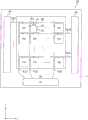
如图1所示,有源矩阵基板100具有显示区域DR和周边区域(有时也称为“边框区域”)FR。显示区域DR包含排列为矩阵状的多个像素区域PIX。像素区域(有时也简称为“像素”)PIX是与显示装置的像素对应的区域。周边区域FR位于显示区域DR的周围。As shown in FIG. 1 , the
在显示区域DR中形成有:在x方向(行方向)上延伸的多个栅极总线GL(1)~GL(j)(j为2以上的整数,以下统称为“栅极总线 GL”)和在y方向(列方向)上延伸的多个源极总线SL(1)~SL(k) (k为2以上的整数,以下统称为“源极总线SL”)。各像素区域PIX例如由栅极总线GL及源极总线SL来规定。各栅极总线GL连接到栅极驱动器GD的各端子。各源极总线SL连接到源极驱动器SD的各端子。In the display region DR, a plurality of gate bus lines GL( 1 ) to GL(j) extending in the x direction (row direction) are formed (j is an integer of 2 or more, hereinafter collectively referred to as “gate bus lines GL”). and a plurality of source bus lines SL( 1 ) to SL(k) extending in the y direction (column direction) (k is an integer greater than or equal to 2, hereinafter collectively referred to as “source bus lines SL”). Each pixel area PIX is defined by, for example, the gate bus line GL and the source bus line SL. Each gate bus line GL is connected to each terminal of the gate driver GD. Each source bus line SL is connected to each terminal of the source driver SD.
有源矩阵基板100具备基板1和支撑于基板1并配置于各像素区域PIX的像素TFTPt。像素TFTPt是包含氧化物半导体层作为活性层的氧化物半导体TFT。The
各像素区域PIX除了具有上述像素TFTPt之外,还具有像素电极 PE。像素TFTPt的栅极电极电连接到对应的栅极总线GL。像素TFTPt 的源极电极电连接到对应的源极总线SL。像素TFTPt的漏极电极电连接到像素电极PE。在将有源矩阵基板100用于FFS(FringeField Switching:边缘场开关)模式等横向电场模式的液晶显示装置的情况下,在有源矩阵基板100上,对于多个像素设置共用的电极(共用电极)CE。Each pixel region PIX has a pixel electrode PE in addition to the above-mentioned pixel TFTPt. The gate electrodes of the pixels TFTPt are electrically connected to the corresponding gate bus lines GL. The source electrodes of the pixels TFTPt are electrically connected to the corresponding source bus lines SL. The drain electrode of the pixel TFTPt is electrically connected to the pixel electrode PE. When the
在周边区域FR中一体地(单片地)设置有驱动栅极总线GL的栅极驱动器GD。虽未图示,但在周边区域FR中也可以一体地设置有分时驱动源极总线SL的源极切换(SourceShared driving:SSD)电路等周边电路。A gate driver GD for driving the gate bus line GL is provided integrally (monolithically) in the peripheral region FR. Although not shown, peripheral circuits such as a source switching (Source Shared driving: SSD) circuit that drives the source bus line SL in a time-sharing manner may be integrally provided in the peripheral region FR.
以下,说明有源矩阵基板100的像素区域PIX的具体结构。Hereinafter, the specific structure of the pixel region PIX of the
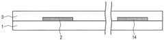
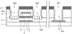
图2是示意性地示出有源矩阵基板100的截面图。在图2的左侧示出显示区域DR的像素区域PIX的一部分,在图2的右侧示出周边区域 FR的一部分。有源矩阵基板100例如用于FFS模式的液晶显示装置。FIG. 2 is a cross-sectional view schematically showing the
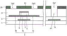
如图2所示,像素区域PIX具有遮光层2、像素TFT(氧化物半导体TFT)Pt、像素电极PE以及共用电极CE。As shown in FIG. 2 , the pixel region PIX has a
遮光层2设置在基板1上。遮光层2具有导电性。以覆盖遮光层2 的方式设置有下部绝缘层3。The
像素电极TFTPt具有氧化物半导体层4、栅极绝缘层5、栅极电极 (上部栅极电极)6、源极电极7以及漏极电极8。像素TFTPt具有顶栅结构。The pixel electrode TFTPt has an
氧化物半导体层4设置于下部绝缘层3上。氧化物半导体层4包含沟道区域4a、源极接触区域4b以及漏极接触区域4c。沟道区域4a当从基板面法线方向观看时与遮光层2重叠。源极接触区域4b及漏极接触区域4c分别位于沟道区域4的两侧。The
栅极绝缘层5设置于氧化物半导体层4的沟道区域4a上。栅极电极 6设置于栅极绝缘层5上。以覆盖栅极电极6及氧化物半导体层4的方式设置有第1层间绝缘层9。The
源极电极7在形成于第1层间绝缘层9的源极接触孔CHs中连接到源极接触区域4b。漏极电极8在形成于第1层间绝缘层9的漏极接触孔 CHd中连接到漏极接触区域4c。The
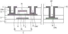
以覆盖像素TFTPt的方式形成有第2层间绝缘层10。如图2所示,第2层间绝缘层10具有包含无机绝缘层(钝化层)11和设置于无机绝缘层11上的有机绝缘层(平坦化层)12的层叠结构。The second
共用电极CE设置于第2层间绝缘层10上。以覆盖共用电极CE的方式设置有电介质层13。The common electrode CE is provided on the second
像素电极PE设置于电介质层13上。像素电极PE在形成于电介质层13及第2层间绝缘层10的像素接触孔CHp中连接到像素TFTPt的漏极电极8。在此虽未图示,但像素电极PE具有至少1个狭缝(开口部)。The pixel electrode PE is disposed on the
周边区域FR具有连接下部导电层14与上部导电层15的连接部CP。下部导电层14与遮光层2由相同导电膜形成。上部导电层15与源极电极7及漏极电极8由相同导电膜形成。上部导电层15在形成于第1层间绝缘层9及下部绝缘层3的连接部接触孔CHc中连接到下部导电层14。连接部CP例如是用于将栅极总线GL或源极总线SL与外部配线电连接的端子部。The peripheral region FR has a connection portion CP that connects the lower
在图2中虽未图示,但在周边区域FR中配置有栅极驱动器GD等单片地形成的周边电路。构成周边电路的TFT(称为“电路TFT”) 也可以与像素TFTPt同样地是氧化物半导体TFT。Although not shown in FIG. 2 , peripheral circuits such as gate drivers GD and the like that are formed monolithically are arranged in the peripheral region FR. The TFT (referred to as "circuit TFT") constituting the peripheral circuit may be an oxide semiconductor TFT similarly to the pixel TFTPt.
有源矩阵基板100用于例如FFS模式或IPS模式的液晶显示装置。 FFS模式是在一个基板上设置一对电极而对液晶分子在与基板面平行的方向(横向)上施加电场的横向电场方式的模式。在该例中,生成由从像素电极PE出发并经过液晶层(未图示)进而经过像素电极PE的狭缝状开口到达共用电极CE的电力线表示的电场。该电场具有相对于液晶层为横向的成分。其结果是,能够对液晶层施加横向的电场。在横向电场方式中,液晶分子不会从基板立起,因此,有能够实现比纵向电场方式宽的视角的优点。The
在共用电极CE上隔着电介质层13配置像素电极PE的电极结构例如公开于国际公开第2012/086513号中。此外,也可以在像素电极PE 上隔着电介质层13配置有共用电极CE。这种电极结构例如记载于特开2008-032899号公报、特开2010-008758号公报。为了参考,将国际公开第2012/086513号、特开2008-032899号公报以及特开 2010-008758号公报的全部公开内容引用到本说明书中。The electrode structure in which the pixel electrode PE is arranged on the common electrode CE with the
参照图3A~图9B来说明本实施方式的有源矩阵基板100的制造方法。图3A~图9B是用于说明有源矩阵基板100的制造方法的工序截面图。A method of manufacturing the
首先,如图3A所示,在基板1上形成遮光层2及下部导电层14。具体地,在具有绝缘性的基板1上通过溅射法等形成遮光层用导电膜 (厚度:例如50nm以上500nm以下),之后将该导电膜图案化,从而能够形成遮光层2及下部导电层14。First, as shown in FIG. 3A , the
作为基板1,例如能够使用玻璃基板、硅基板、具有耐热性的塑料基板(树脂基板)等。As the
作为遮光层用导电膜,例如能够使用包含从铝(Al)、铬(Cr)、铜(Cu)、钽(Ta)、钛(Ti)、钼(Mo)或者钨(W)选出的元素的金属膜、或者以这些元素为成分的合金膜等。另外,也可以使用包含其中的多个膜的层叠膜。例如,能够使用具有钛膜-铝膜-钛膜的3 层结构或者钼膜-铝膜-钼膜的3层结构的层叠膜。此外,遮光层用导电膜不限于3层结构,也可以具有单层或2层结构、或者4层以上的层叠结构。在此,使用以Ti膜(厚度:15~70nm)为下层、以Cu膜(厚度:200~400nm)为上层的层叠膜作为遮光层用导电膜。As the conductive film for the light shielding layer, for example, an element containing an element selected from aluminum (Al), chromium (Cr), copper (Cu), tantalum (Ta), titanium (Ti), molybdenum (Mo), or tungsten (W) can be used metal films, or alloy films containing these elements. In addition, a laminated film comprising a plurality of films therein may also be used. For example, a laminated film having a three-layer structure of titanium film-aluminum film-titanium film or a three-layer structure of molybdenum film-aluminum film-molybdenum film can be used. In addition, the conductive film for light shielding layers is not limited to a three-layer structure, and may have a single-layer or two-layer structure, or a laminated structure of four or more layers. Here, a laminated film having a Ti film (thickness: 15 to 70 nm) as a lower layer and a Cu film (thickness: 200 to 400 nm) as an upper layer was used as the light-shielding layer conductive film.
接着,如图3B所示,以覆盖遮光层2及下部导电层14的方式形成下部绝缘层3(厚度:例如200nm以上500nm以下)。Next, as shown in FIG. 3B , the lower insulating layer 3 (thickness: for example, 200 nm or more and 500 nm or less) is formed so as to cover the
作为下部绝缘层3,能够适当地使用氧化硅(SiO2)层、氮化硅 (SiNx)层、氧化氮化硅(SiOxNy:x>y)层、氮化氧化硅(SiNxOy: x>y)层、氧化铝层或者氧化钽层等。下部绝缘层3也可以具有层叠结构。在此,例如使用CVD法形成下部绝缘层3,并且下部绝缘层3 具有形成以氮化硅(SiNx)层(厚度:100~500nm)为下层、以氧化硅(SiO2)层(厚度:20~300nm)为上层的层叠膜的结构。As the lower insulating
接下来,在下部绝缘层3上形成氧化物半导体层4、栅极绝缘层5 以及栅极电极6。Next, the
具体地,首先,如图3C所示,在下部绝缘层3上按顺序形成氧化物半导体膜4'(厚度:例如15nm以上200nm以下)、绝缘膜5'(厚度:例如80nm以上250nm以下)以及栅极用导电膜6'(厚度:例如50nm 以上500nm以下)。氧化物半导体膜4'及栅极用导电膜6'例如可以通过溅射法形成,绝缘膜5'例如可以通过CVD法形成。氧化物半导体膜4' 没有特别限定,例如是In-Ga-Zn-O系半导体膜。作为绝缘膜5',能够使用与下部绝缘层3同样的绝缘膜(作为下部绝缘层5而例示出的绝缘膜)。作为栅极用导电膜6',能够使用与遮光层用导电膜同样的导电膜。在此,作为绝缘膜5',使用例如氧化硅(SiO2)膜,作为栅极用导电膜6',使用以Ti膜(厚度:15~70nm)为下层、以Cu层(厚度:200~400nm)为上层的层叠膜。Specifically, first, as shown in FIG. 3C , an
接着,如图3D所示,依次通过栅极用导电膜6'的图案化进行栅极电极6的形成、以及通过绝缘膜5'的图案化进行栅极绝缘层5的形成。例如能够通过湿式蚀刻或者干式蚀刻进行栅极用导电膜6'的图案化。例如能够通过干式蚀刻进行绝缘膜5'的图案化。Next, as shown in FIG. 3D , the
接下来,如图4A所示,进行氧化物半导体膜4'的图案化,从而形成氧化物半导体层4。例如能够通过湿式蚀刻进行氧化物半导体膜4' 的图案化。之后,以栅极电极6为掩模进行氧化物半导体层4的低电阻化处理。低电阻化处理例如是等离子体处理。由此,氧化物半导体层4中的与栅极电极6及栅极绝缘层5不重叠的区域成为电阻率比与栅极电极6及栅极绝缘层5重叠的区域(沟道区域4a)的电阻率低的低电阻区域(源极接触区域4b及漏极接触区域4c)。Next, as shown in FIG. 4A , the
接着,如图4B所示,以覆盖氧化物半导体层4、栅极绝缘层5以及栅极电极6的方式形成第1层间绝缘层9。第1层间绝缘层9的厚度例如是100nm以上500nm以下。作为第1层间绝缘层9,能够使氧化硅膜、氮化硅膜、氧化氮化硅膜、氮化氧化硅膜以单层或者层叠形成。在此,作为第1层间绝缘层9,例如通过CVD法形成SiNx层(厚度:300nm)。Next, as shown in FIG. 4B , the first
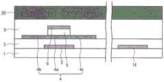
接下来,以使氧化物半导体层4的源极接触区域4b的一部分及漏极接触区域4c的一部分露出的方式将源极接触孔CHs及漏极接触孔 CHd形成于第1层间绝缘层9,并且以使下部导电层14的一部分露出的方式将连接部接触孔CHc形成于第1层间绝缘层9及下部绝缘层3。具体地,首先如图4C所示,在第1层间绝缘层9上形成光致抗蚀剂膜20'。Next, a source contact hole CHs and a drain contact hole CHd are formed in the first
接着,如图5A所示,使用多灰度级掩模将光致抗蚀剂膜20'曝光,之后进行显影,从而形成光致抗蚀剂层20。光致抗蚀剂层20具有:第1区域R1,其具有第1厚度t1;第2区域R2及第3区域R3,其具有比第1厚度t1小的第2厚度t2,分别与源极接触区域4b的一部分及漏极接触区域4c的一部分重叠;以及第1开口部Op1,其与下部导电层14的一部分重叠。作为多灰度级掩模,具体地,能够使用灰色调掩模(Gray tone Mask)或半色调掩模(Halftone Mask)。在灰色调掩模中形成有曝光机的分辨率以下的狭缝,通过该狭缝遮挡光的一部分从而实现中间曝光。另一方面,半色调掩模通过使用半透射膜从而实现中间曝光。Next, as shown in FIG. 5A , the
接下来,如图5B所示,通过蚀刻(例如干式蚀刻)在第1层间绝缘层9形成从光致抗蚀剂层20的第1开口部Op1延伸的第1孔H1。第1 孔H1从第1开口部Op1延伸而到达下部绝缘层3的上表面。Next, as shown in FIG. 5B , a first hole H1 extending from the first opening Op1 of the
接着,如图6A所示,除去光致抗蚀剂层20的第2区域R2及第3区域R3,从而在光致抗蚀剂层20形成第2开口部Op2及第3开口部Op3。该工序例如能够通过灰化来进行。Next, as shown in FIG. 6A , the second and third openings Op2 and Op3 are formed in the
接下来,如图6B所示,通过蚀刻(例如干式蚀刻),在下部绝缘层3形成从第1层间绝缘层9的第1孔H1延伸的第2孔H2,并且在第1层间绝缘层9形成从光致抗蚀剂层20的第2开口部Op2延伸的第3孔H3、以及从光致抗蚀剂层20的第3开口部Op3延伸的第4孔H4。第2孔H2从第1层间绝缘层9的第1孔H1延伸而到达下部导电层14的上表面。第3 孔H3从光致抗蚀剂层20的第2开口部Op2延伸而到达氧化物半导体层 4的源极接触区域4b的上表面。第4孔H4从光致抗蚀剂层20的第3开口部Op3延伸而到达氧化物半导体层4的漏极接触区域4c的上表面。之后,光致抗蚀剂层20被剥离。Next, as shown in FIG. 6B , a second hole H2 extending from the first hole H1 of the first
这样,能够将源极接触孔Chs及漏极接触孔CHd形成于第1层间绝缘层9,并且能够将连接部接触孔CHc形成于第1层间绝缘层9及下部绝缘层3。In this way, the source contact hole Chs and the drain contact hole CHd can be formed in the first
接着,如图7A所示,在第1层间绝缘层9上形成源极电极7、漏极电极8以及上部导电层15。具体地,在第1层间绝缘层9上、源极接触孔CHs内、漏极接触孔CHd内以及连接部接触孔CHc内形成源极用导电膜(厚度:例如50nm以上500nm以下),之后将源极用导电膜图案化,从而能够形成源极电极7、漏极电极8以及上部导电层15。能够通过例如干式蚀刻或者湿式蚀刻来进行源极用导电膜的图案化。作为源极用导电膜,例如能够使用从铝(Al)、铬(Cr)、铜(Cu)、钽(Ta)、钛(Ti)、钼(Mo)或者钨(W)选出的元素、或者以这些元素为成分的合金等。例如,可以具有钛膜-铝膜-钛膜的3层结构、钼膜-铝膜-钼膜等3层结构等。此外,源极用导电膜不限于3层结构,也可以具有单层或2层结构、或者4层以上的层叠结构。在此,使用以Ti膜(厚度:15~70nm)为下层、以Cu膜(厚度:200~400nm) 为上层的层叠膜。Next, as shown in FIG. 7A , the
接下来,如图7B所示,以覆盖像素TFTPt的方式形成第2层间绝缘层10。具体地,依次形成无机绝缘层11(厚度:例如100nm以上 400nm以下)及有机绝缘层12(厚度:例如1~3μm、优选2~3μm),从而形成第2层间绝缘层10。在有机绝缘层12形成有与漏极电极8的至少一部分重叠的开口部12a。无机绝缘层11的材料可以与作为第1 层间绝缘层9的材料而例示出的材料相同。在此,作为无机绝缘层11,通过CVD法形成SiNx层(厚度:例如200nm)。有机绝缘层12例如由感光性树脂材料形成。Next, as shown in FIG. 7B , the second
接着,如图8A所示,在第2层间绝缘层10上形成共用电极CE。具体地,在第2层间绝缘层10上形成透明导电膜(厚度:20~30nm),之后将透明导电膜图案化,从而能够形成共用电极CE。在此,例如在通过溅射法形成铟-锌氧化物膜作为透明导电膜之后,通过湿式蚀刻进行图案化。作为透明电极膜的材料,能够使用铟-锡氧化物(ITO)、铟-锌氧化物、ZnO等金属氧化物。Next, as shown in FIG. 8A , the common electrode CE is formed on the second
接下来,如图8B所示,在第2层间绝缘层10及共用电极CE上形成电介质层13(厚度:50~500nm)。电介质层13的材料可以与作为第1 层间绝缘层9的材料而例示出的材料相同。在此,作为电介质层13,例如通过CVD法形成SiN膜。Next, as shown in FIG. 8B , a dielectric layer 13 (thickness: 50 to 500 nm) is formed on the second
接着,如图9A所示,在电介质层13及无机绝缘层11上,以使漏极电极8的一部分露出的方式形成像素接触孔CHp。例如能够通过干式蚀刻来进行像素接触孔CHp的形成。Next, as shown in FIG. 9A , on the
之后,如图9B所示,在电介质层13上形成像素电极PE(厚度: 20~300nm)。具体地,在电介质层13上形成透明导电膜,之后将透明导电膜图案化,从而形成像素电极PE。像素电极PE用的透明导电膜的材料可以与作为共用电极CE用的透明导电膜的材料而例示出的材料相同。在此,通过溅射法形成铟-锌氧化物膜作为透明导电膜,之后通过湿式蚀刻进行图案化。After that, as shown in FIG. 9B , a pixel electrode PE (thickness: 20 to 300 nm) is formed on the
这样,能够得到有源矩阵基板100。In this way, the
[关于本发明的第1实施方式的制造方法的效果][About the effects of the manufacturing method of the first embodiment of the present invention]
下面,与参考例的制造方法进行比较来说明本发明的第1实施方式的制造方法的效果。Next, the effect of the manufacturing method of the first embodiment of the present invention will be described in comparison with the manufacturing method of the reference example.
图10A~图11B是用于说明参考例的制造方法的示意性工序截面图。10A to 11B are schematic process cross-sectional views for explaining the manufacturing method of the reference example.
在参考例的制造方法中,首先,如图10A所示,在基板1上形成遮光层2、下部导电层14、下部绝缘层3、氧化物半导体层4、栅极绝缘层5、栅极电极6以及第1层间绝缘层9。该工序能够通过参照图3A~图4B所说明的方法来进行。接着,如图10B所示,在第1层间绝缘层9 上形成光致抗蚀剂膜21'。In the manufacturing method of the reference example, first, as shown in FIG. 10A , the
接下来,如图11A所示,使用光掩模将光致抗蚀剂膜21'曝光,之后进行显影,从而形成光致抗蚀剂层21。在此使用的光掩模不是多灰度级掩模而是普通的二元掩模(BinaryMask)。所得到的光致抗蚀剂层21具有:第1开口部Op1,其与下部导电层14的一部分重叠;以及第2开口部Op2及第3开口部Op3,其分别与源极接触区域4b的一部分及漏极接触区域4c的一部分重叠。Next, as shown in FIG. 11A , the
接着,如图11B所示,通过蚀刻,在第1层间绝缘层9形成源极接触孔CHs及漏极接触孔CHd,并且在第1层间绝缘层9及下部绝缘层3 形成连接部接触孔CHc。Next, as shown in FIG. 11B , by etching, source contact holes CHs and drain contact holes CHd are formed in the first
之后,将光致抗蚀剂层21剥离,通过参照图7A~图10B所说明的方法,形成源极电极7、漏极电极8、上部导电层15、第2层间绝缘层 10、共用电极CE、电介质层13以及像素电极PE。After that, the
在参考例的制造方法中,在形成连接部接触孔CHc时,下部绝缘层3和第1层间绝缘层9一并被蚀刻,因此,蚀刻时间变长。所以,如在图12中示意性地示出的那样,接触孔(源极接触孔CHs、漏极接触孔CHd以及连接部接触孔CHc)的尺寸变大,产生设计上的困难。另外,在各像素PIX中,虽然氧化物半导体层4会作为针对下部绝缘层3 的蚀刻阻挡物发挥功能,但在氧化物半导体层4未能承受住蚀刻的情况下,如图12所示,直至下部绝缘层3均会被蚀刻。下部绝缘层3的过蚀刻成为可靠性降低的原因。In the manufacturing method of the reference example, when the connection portion contact hole CHc is formed, the lower insulating
相对于此,在本发明的第1实施方式的制造方法中,在形成源极接触孔CHs、漏极接触孔CHd以及连接部接触孔CHc的工序中,通过使用多灰度级掩模,从而会形成具有第1区域R1、比第1区域R1薄的第2区域R2及第3区域R3、以及第1开口部Op1的光致抗蚀剂层20。由此,如已经说明的那样,由于无需一并蚀刻第1层间绝缘层9及下部绝缘层3,因此,能够防止接触孔(源极接触孔CHs、漏极接触孔CHd 以及连接部接触孔CHc)的尺寸变大。另外,由于无需使用氧化物半导体层4作为一并蚀刻时的针对下部绝缘层3的蚀刻阻挡物,因此,还能防止下部绝缘层3被蚀刻,能够抑制由下部绝缘层3的过蚀刻导致的可靠性降低。而且,由于无需一并蚀刻第1层间绝缘层9及下部绝缘层3,因此,与参考例的制造方法相比,可以分别较厚地形成第 1层间绝缘层9及下部绝缘层3。通过较厚地形成第1层间绝缘层9及下部绝缘层3,能够提高成品率。On the other hand, in the manufacturing method according to the first embodiment of the present invention, in the step of forming the source contact hole CHs, the drain contact hole CHd, and the connection portion contact hole CHc, by using a multi-gradation mask, A
[关于对遮光层2提供的电位][Regarding the potential supplied to the light shielding layer 2]
具有导电性的遮光层2既可以是电浮动状态(浮置;Floating),也可以是被提供规定的电位。通过对遮光层2提供规定的电位(固定电位),能够提高像素TFTPt的TFT特性。另外,也可以对遮光层2提供与栅极电极(上部栅极电极)6实质上相同的电位,使其作为下部栅极电极发挥功能。即,也可以将像素TFTPt设为双栅结构。The
(实施方式2)(Embodiment 2)
参照图13A~图14B说明本发明的第2实施方式的制造方法。图 13A~图14B是用于说明本实施方式的制造方法的工序截面图。在以下的说明中,以与实施方式1的制造方法的不同之处为中心进行本实施方式的制造方法的说明。A manufacturing method according to the second embodiment of the present invention will be described with reference to FIGS. 13A to 14B . 13A to 14B are process cross-sectional views for explaining the manufacturing method of the present embodiment. In the following description, the manufacturing method of the present embodiment will be described focusing on the differences from the manufacturing method of the first embodiment.
首先,如图13A所示,在基板1上形成遮光层2、下部导电层14、下部绝缘层3、氧化物半导体层4、栅极绝缘层5、栅极电极6以及第1 层间绝缘层9,进而在第1层间绝缘层9上形成光致抗蚀剂层20,光致抗蚀剂层20具有第1区域R1、第2区域R2及第3区域R3、以及第1开口部Op1。该工序能够通过参照图3A~图5A所说明的方法来进行。即,在当形成光致抗蚀剂层20时,可以使用多灰度级掩模。First, as shown in FIG. 13A , the
接着,如图13B所示,通过蚀刻(例如干式蚀刻)在第1层间绝缘层9及下部绝缘层3形成从光致抗蚀剂层20的第1开口部Op1延伸的第1孔H1。第1孔H1从第1开口部Op1延伸而到达下部导电层14的上表面。Next, as shown in FIG. 13B , a first hole H1 extending from the first opening Op1 of the
接着,如图14A所示,除去光致抗蚀剂层20的第2区域R2及第3 区域R3,从而在光致抗蚀剂层20形成第2开口部Op2及第3开口部Op3。该工序例如能够通过灰化来进行。Next, as shown in FIG. 14A , the second and third openings Op2 and Op3 are formed in the
接下来,如图14B所示,通过蚀刻(例如干式蚀刻),在第1层间绝缘层9形成从光致抗蚀剂层20的第2开口部Op2延伸的第2孔H2、以及从光致抗蚀剂层20的第3开口部Op3延伸的第3孔H3。第2孔H2从光致抗蚀剂层20的第2开口部Op2延伸而到达氧化物半导体层4的源极接触区域4b的上表面。第3孔H3从光致抗蚀剂层20的第3开口部Op3 延伸而到达氧化物半导体层4的漏极接触区域4c的上表面。之后,光致抗蚀剂层20被剥离。Next, as shown in FIG. 14B , a second hole H2 extending from the second opening Op2 of the
这样,能够将源极接触孔CHs及漏极接触孔CHd形成于第1层间绝缘层9,并且能够将连接部接触孔CHc形成于第1层间绝缘层9及下部绝缘层3。In this way, the source contact hole CHs and the drain contact hole CHd can be formed in the first
之后,通过参照图7A~图10B所说明的方法,形成源极电极7、漏极电极8、上部导电层15、第2层间绝缘层10、共用电极CE、电介质层13以及像素电极PE,从而可以得到有源矩阵基板100。Then, by the method described with reference to FIGS. 7A to 10B , the
本实施方式的制造方法与实施方式1的制造方法的不同之处在于:在形成连接部接触孔CHc时,一并蚀刻第1层间绝缘层9及下部绝缘层3。在对第1层间绝缘层9及下部绝缘层3一并进行蚀刻时,在光致抗蚀剂层20未形成有第2开口部Op2及第3开口部Op3(即,存在有第2区域R2及第3区域R3),因此,与参考例的制造方法不同,未将氧化物半导体层4用作针对下部绝缘层9的蚀刻阻挡物。因而,能够防止氧化物半导体层4未能承受住蚀刻而直至下部绝缘层3均被蚀刻。因此,能够抑制由下部绝缘层3的过蚀刻导致的可靠性降低。The manufacturing method of this embodiment differs from the manufacturing method of
此外,在本实施方式的制造方法中,在下部导电层14露出的状态下进行用于形成源极接触孔CHs(第2孔H2)及漏极接触孔CHd(第 3孔H3)的蚀刻(图14B)。因此,担心会对下部导电层14造成损伤。因而,从不对下部导电层14带来损伤的观点来看,可以说优选实施方式1的制造方法。Further, in the manufacturing method of the present embodiment, etching for forming the source contact hole CHs (second hole H2 ) and the drain contact hole CHd (third hole H3 ) is performed with the lower
[关于氧化物半导体][About oxide semiconductors]
在上述的所有实施方式中,氧化物半导体既可以是非晶质氧化物半导体,也可以是具有结晶质部分的结晶质氧化物半导体。作为结晶质氧化物半导体,可以列举多晶氧化物半导体、微晶氧化物半导体、c轴与层面大致垂直地取向的结晶质氧化物半导体等。In all the above-described embodiments, the oxide semiconductor may be either an amorphous oxide semiconductor or a crystalline oxide semiconductor having a crystalline portion. Examples of the crystalline oxide semiconductor include polycrystalline oxide semiconductors, microcrystalline oxide semiconductors, and crystalline oxide semiconductors in which the c-axis is oriented substantially perpendicular to the plane surface.
氧化物半导体层也可以具有2层以上的层叠结构。在氧化物半导体层具有层叠结构的情况下,氧化物半导体层可以包含非晶质氧化物半导体层和结晶质氧化物半导体层。或者,也可以包含结晶结构不同的多个结晶质氧化物半导体层。另外,也可以包含多个非晶质氧化物半导体层。在氧化物半导体层具有包含上层和下层的2层结构的情况下,2层中的位于栅极电极侧的层(若是底栅结构则为下层,若是顶栅结构则为上层)所包含的氧化物半导体的能隙可以小于位于与栅极电极相反的一侧的层(若是底栅结构则为上层,若是顶栅结构则为下层)所包含的氧化物半导体的能隙。不过,在这些层的能隙之差比较小的情况下,位于栅极电极侧的层的氧化物半导体的能隙也可以大于位于与栅极电极相反的一侧的层的氧化物半导体的能隙。The oxide semiconductor layer may have a stacked structure of two or more layers. In the case where the oxide semiconductor layer has a stacked structure, the oxide semiconductor layer may include an amorphous oxide semiconductor layer and a crystalline oxide semiconductor layer. Alternatively, a plurality of crystalline oxide semiconductor layers having different crystal structures may be included. In addition, a plurality of amorphous oxide semiconductor layers may be included. In the case where the oxide semiconductor layer has a two-layer structure including an upper layer and a lower layer, among the two layers, the layer on the gate electrode side (the lower layer in the case of the bottom gate structure, the upper layer in the case of the top gate structure) contains oxide The energy gap of the material semiconductor may be smaller than the energy gap of the oxide semiconductor contained in the layer on the opposite side to the gate electrode (the upper layer in the case of the bottom gate structure, and the lower layer in the case of the top gate structure). However, when the difference between the energy gaps of these layers is relatively small, the energy gap of the oxide semiconductor of the layer located on the gate electrode side may be larger than that of the oxide semiconductor of the layer located on the opposite side to the gate electrode. gap.
非晶质氧化物半导体及上述的各结晶质氧化物半导体的材料、结构、成膜方法、具有层叠结构的氧化物半导体层的构成等记载于例如特开2014-007399号公报中。为了参考,将特开2014-007399号公报的所有公开内容引用到本说明书中。The materials, structures, film-forming methods of amorphous oxide semiconductors and the above-mentioned crystalline oxide semiconductors, structures of oxide semiconductor layers having a stacked structure, and the like are described in, for example, Japanese Patent Laid-Open No. 2014-007399. For reference, the entire disclosure of JP-A-2014-007399 is incorporated herein by reference.
氧化物半导体层例如可以包含In、Ga以及Zn中的至少1种金属元素。在本实施方式中,氧化物半导体层例如包含In-Ga-Zn-O系半导体(例如氧化铟镓锌)。在此,In-Ga-Zn-O系半导体是In(铟)、Ga(镓)、 Zn(锌)的三元系氧化物,并且In、Ga以及Zn的比例(组成比)没有特别限定,例如包含In:Ga:Zn=2:2:1、In:Ga:Zn=1:1:1、 In:Ga:Zn=1:1:2等。这种氧化物半导体层可以由包含In-Ga-Zn-O 系半导体的氧化物半导体膜形成。此外,有时将具有包含In-Ga-Zn-O 系半导体等氧化物半导体的活性层的沟道蚀刻型TFT称为“CE-OS-TFT”。The oxide semiconductor layer may contain, for example, at least one metal element selected from In, Ga, and Zn. In the present embodiment, the oxide semiconductor layer includes, for example, an In-Ga-Zn-O-based semiconductor (eg, indium gallium zinc oxide). Here, the In-Ga-Zn-O-based semiconductor is a ternary system oxide of In (indium), Ga (gallium), and Zn (zinc), and the ratio (composition ratio) of In, Ga, and Zn is not particularly limited, For example, In:Ga:Zn=2:2:1, In:Ga:Zn=1:1:1, In:Ga:Zn=1:1:2, etc. are included. Such an oxide semiconductor layer can be formed of an oxide semiconductor film containing an In-Ga-Zn-O-based semiconductor. In addition, a channel-etched TFT having an active layer containing an oxide semiconductor such as an In-Ga-Zn-O-based semiconductor may be referred to as "CE-OS-TFT".
In-Ga-Zn-O系半导体既可以是非晶质,也可以是结晶质。作为结晶质In-Ga-Zn-O系半导体,优选c轴与层面大致垂直地取向的结晶质 In-Ga-Zn-O系半导体。The In-Ga-Zn-O-based semiconductor may be amorphous or crystalline. As the crystalline In-Ga-Zn-O-based semiconductor, a crystalline In-Ga-Zn-O-based semiconductor in which the c-axis is oriented substantially perpendicular to the plane surface is preferable.
此外,结晶质In-Ga-Zn-O系半导体的结晶结构例如公开于上述的特开2014-007399号公报、特开2012-134475号公报、特开2014-209727 号公报等。为了参考,将特开2012-134475号公报及特开2014-209727 号公报的全部公开内容引用到本说明书中。具有In-Ga-Zn-O系半导体层的TFT具有高迁移率(与a-SiTFT相比超过20倍)及低漏电流(与 a-SiTFT相比不到百分之一),因此,适合用作驱动TFT(例如,在包含多个像素的显示区域的周边设置于与显示区域相同的基板上的驱动电路所包含的TFT)及像素TFT(设置于像素的TFT)。Further, the crystal structure of the crystalline In-Ga-Zn-O-based semiconductor is disclosed in, for example, the above-mentioned Japanese Patent Laid-Open No. 2014-007399, Japanese Patent Laid-Open No. 2012-134475, and Japanese Patent Laid-Open No. 2014-209727. For reference, the entire disclosure contents of JP-A No. 2012-134475 and JP-A No. 2014-209727 are incorporated herein by reference. TFTs with In-Ga-Zn-O-based semiconductor layers have high mobility (more than 20 times compared to a-SiTFT) and low leakage current (less than 1% compared to a-SiTFT), so they are suitable for It is used as a driver TFT (for example, a TFT included in a driver circuit provided on the same substrate as the display area around a display area including a plurality of pixels) and a pixel TFT (a TFT provided on a pixel).
氧化物半导体层也可以包含其它氧化物半导体来代替 In-Ga-Zn-O系半导体。例如也可以包含In-Sn-Zn-O系半导体(例如 In2O3-SnO2-ZnO;InSnZnO)。In-Sn-Zn-O系半导体是In(铟)、Sn(锡) 以及Zn(锌)的三元系氧化物。或者,氧化物半导体层也可以包含 In-Al-Zn-O系半导体、In-Al-Sn-Zn-O系半导体、Zn-O系半导体、In- Zn-O系半导体、Zn-Ti-O系半导体、Cd-Ge-O系半导体、Cd-Pb-O系半导体、CdO(氧化镉)、Mg-Zn-O系半导体、In-Ga-Sn-O系半导体、 In-Ga-O系半导体、Zr-In-Zn-O系半导体、Hf-In-Zn-O系半导体、 Al-Ga-Zn-O系半导体、Ga-Zn-O系半导体等。The oxide semiconductor layer may contain other oxide semiconductors instead of the In-Ga-Zn-O-based semiconductor. For example, an In-Sn-Zn-O-based semiconductor (eg, In2 O3 -SnO2 -ZnO; InSnZnO) may be included. The In-Sn-Zn-O-based semiconductor is a ternary system oxide of In (indium), Sn (tin), and Zn (zinc). Alternatively, the oxide semiconductor layer may include In-Al-Zn-O-based semiconductor, In-Al-Sn-Zn-O-based semiconductor, Zn-O-based semiconductor, In-Zn-O-based semiconductor, Zn-Ti-O System semiconductors, Cd-Ge-O-based semiconductors, Cd-Pb-O-based semiconductors, CdO (cadmium oxide), Mg-Zn-O-based semiconductors, In-Ga-Sn-O-based semiconductors, In-Ga-O-based semiconductors , Zr-In-Zn-O series semiconductor, Hf-In-Zn-O series semiconductor, Al-Ga-Zn-O series semiconductor, Ga-Zn-O series semiconductor, etc.
根据本发明的实施方式,能够提供一种适合用于制造具备沟道遮光层和具有上部栅极电极的氧化物半导体TFT的有源矩阵基板的方法。According to an embodiment of the present invention, it is possible to provide a method suitable for manufacturing an active matrix substrate having a channel light shielding layer and an oxide semiconductor TFT having an upper gate electrode.
Claims (7)
Applications Claiming Priority (2)
| Application Number | Priority Date | Filing Date | Title |
|---|---|---|---|
| US201962822192P | 2019-03-22 | 2019-03-22 | |
| US62/822,192 | 2019-03-22 |
Publications (2)
| Publication Number | Publication Date |
|---|---|
| CN111722446Atrue CN111722446A (en) | 2020-09-29 |
| CN111722446B CN111722446B (en) | 2023-01-31 |
Family
ID=72514003
Family Applications (1)
| Application Number | Title | Priority Date | Filing Date |
|---|---|---|---|
| CN202010186575.2AActiveCN111722446B (en) | 2019-03-22 | 2020-03-17 | Method for manufacturing active matrix substrate |
Country Status (2)
| Country | Link |
|---|---|
| US (1) | US11145679B2 (en) |
| CN (1) | CN111722446B (en) |
Cited By (1)
| Publication number | Priority date | Publication date | Assignee | Title |
|---|---|---|---|---|
| CN115206995A (en)* | 2021-04-09 | 2022-10-18 | 株式会社日本显示器 | Display device |
Families Citing this family (5)
| Publication number | Priority date | Publication date | Assignee | Title |
|---|---|---|---|---|
| KR102704437B1 (en)* | 2019-06-13 | 2024-09-09 | 삼성디스플레이 주식회사 | Thin film transistor substrate and display apparatus comprising the same |
| JP7562434B2 (en)* | 2021-01-25 | 2024-10-07 | 株式会社ジャパンディスプレイ | Semiconductor Device |
| CN113629073B (en)* | 2021-07-27 | 2023-08-01 | 深圳市华星光电半导体显示技术有限公司 | TFT backplane and display panel |
| CN114823726A (en)* | 2022-04-14 | 2022-07-29 | 武汉华星光电技术有限公司 | Display panel and display device |
| JP7461988B2 (en)* | 2022-06-22 | 2024-04-04 | シャープディスプレイテクノロジー株式会社 | Active matrix substrate and display device |
Citations (9)
| Publication number | Priority date | Publication date | Assignee | Title |
|---|---|---|---|---|
| US20120001837A1 (en)* | 2010-07-05 | 2012-01-05 | Mitsubishi Electric Corporation | Active matrix substrate and liquid crystal device |
| CN102576732A (en)* | 2009-07-18 | 2012-07-11 | 株式会社半导体能源研究所 | Semiconductor device and method for manufacturing semiconductor device |
| CN103247659A (en)* | 2012-02-09 | 2013-08-14 | 乐金显示有限公司 | Organic light emitting display device and method for fabricating the same |
| CN103715141A (en)* | 2013-12-27 | 2014-04-09 | 京东方科技集团股份有限公司 | Array substrate and preparation method thereof |
| CN104022077A (en)* | 2014-05-27 | 2014-09-03 | 京东方科技集团股份有限公司 | Array substrate, preparing method thereof and display device |
| KR20140114327A (en)* | 2014-09-05 | 2014-09-26 | 삼성디스플레이 주식회사 | Liquid crystal display and fabricating method of the same |
| US20160300862A1 (en)* | 2008-05-16 | 2016-10-13 | Semiconductor Energy Laboratory Co., Ltd. | Semiconductor device and manufacturing method of the same |
| CN106847744A (en)* | 2017-02-20 | 2017-06-13 | 合肥京东方光电科技有限公司 | The preparation method of array base palte, array base palte and display device |
| CN108780758A (en)* | 2016-03-14 | 2018-11-09 | 夏普株式会社 | The manufacturing method of semiconductor device and semiconductor device |
Family Cites Families (3)
| Publication number | Priority date | Publication date | Assignee | Title |
|---|---|---|---|---|
| CN103500712B (en) | 2010-12-03 | 2016-05-25 | 株式会社半导体能源研究所 | Semiconductor device |
| JP5725337B2 (en) | 2011-03-24 | 2015-05-27 | ソニー株式会社 | Display device, display device manufacturing method, and electronic apparatus |
| WO2018212100A1 (en) | 2017-05-18 | 2018-11-22 | シャープ株式会社 | Active matrix substrate and production method therefor |
- 2020
- 2020-03-17USUS16/820,900patent/US11145679B2/enactiveActive
- 2020-03-17CNCN202010186575.2Apatent/CN111722446B/enactiveActive
Patent Citations (9)
| Publication number | Priority date | Publication date | Assignee | Title |
|---|---|---|---|---|
| US20160300862A1 (en)* | 2008-05-16 | 2016-10-13 | Semiconductor Energy Laboratory Co., Ltd. | Semiconductor device and manufacturing method of the same |
| CN102576732A (en)* | 2009-07-18 | 2012-07-11 | 株式会社半导体能源研究所 | Semiconductor device and method for manufacturing semiconductor device |
| US20120001837A1 (en)* | 2010-07-05 | 2012-01-05 | Mitsubishi Electric Corporation | Active matrix substrate and liquid crystal device |
| CN103247659A (en)* | 2012-02-09 | 2013-08-14 | 乐金显示有限公司 | Organic light emitting display device and method for fabricating the same |
| CN103715141A (en)* | 2013-12-27 | 2014-04-09 | 京东方科技集团股份有限公司 | Array substrate and preparation method thereof |
| CN104022077A (en)* | 2014-05-27 | 2014-09-03 | 京东方科技集团股份有限公司 | Array substrate, preparing method thereof and display device |
| KR20140114327A (en)* | 2014-09-05 | 2014-09-26 | 삼성디스플레이 주식회사 | Liquid crystal display and fabricating method of the same |
| CN108780758A (en)* | 2016-03-14 | 2018-11-09 | 夏普株式会社 | The manufacturing method of semiconductor device and semiconductor device |
| CN106847744A (en)* | 2017-02-20 | 2017-06-13 | 合肥京东方光电科技有限公司 | The preparation method of array base palte, array base palte and display device |
Cited By (2)
| Publication number | Priority date | Publication date | Assignee | Title |
|---|---|---|---|---|
| CN115206995A (en)* | 2021-04-09 | 2022-10-18 | 株式会社日本显示器 | Display device |
| CN115206995B (en)* | 2021-04-09 | 2024-12-10 | 株式会社日本显示器 | Display device |
Also Published As
| Publication number | Publication date |
|---|---|
| CN111722446B (en) | 2023-01-31 |
| US11145679B2 (en) | 2021-10-12 |
| US20200303425A1 (en) | 2020-09-24 |
Similar Documents
| Publication | Publication Date | Title |
|---|---|---|
| CN111722446B (en) | Method for manufacturing active matrix substrate | |
| CN107636841B (en) | Active matrix substrate, manufacturing method thereof, and display device using active matrix substrate | |
| CN110931508B (en) | Active matrix substrate and method for manufacturing same | |
| CN105814481B (en) | Semiconductor device and its manufacturing method | |
| CN110521003B (en) | Active matrix substrate and manufacturing method thereof | |
| CN110931505B (en) | display device | |
| JP7471075B2 (en) | Active matrix substrate and its manufacturing method | |
| CN113257835A (en) | Active matrix substrate and method for manufacturing the same | |
| CN112071860A (en) | Active matrix substrate and method for manufacturing same | |
| WO2017094682A1 (en) | Semiconductor device, and method for manufacturing same | |
| US20210013238A1 (en) | Active matrix substrate and method for manufacturing same | |
| WO2018043426A1 (en) | Active matrix substrate and method for producing same | |
| US11721704B2 (en) | Active matrix substrate | |
| CN112349732A (en) | Active matrix substrate and method for manufacturing the same | |
| CN108496244A (en) | Semiconductor device and its manufacturing method | |
| CN109698205B (en) | Active matrix substrate and manufacturing method thereof | |
| US20210124220A1 (en) | Active matrix substrate, liquid crystal display device with touch sensor using active matrix substrate, and method for manufacturing active matrix substrate | |
| JP7461988B2 (en) | Active matrix substrate and display device | |
| US20250287693A1 (en) | Active matrix substrate, display device and method for manufacturing active matrix substrate | |
| US20230178561A1 (en) | Active matrix substrate and method for manufacturing same | |
| US11817459B2 (en) | Active matrix substrate and manufacturing method thereof | |
| US12443080B2 (en) | Active matrix substrate and display device | |
| JP2022135619A (en) | Active matrix substrate and manufacturing method thereof | |
| JP2023163682A (en) | Active matrix substrate and liquid crystal display device |
Legal Events
| Date | Code | Title | Description |
|---|---|---|---|
| PB01 | Publication | ||
| PB01 | Publication | ||
| SE01 | Entry into force of request for substantive examination | ||
| SE01 | Entry into force of request for substantive examination | ||
| GR01 | Patent grant | ||
| GR01 | Patent grant |