CN111696486B - Pixel driving circuit and driving method thereof, display substrate and display device - Google Patents
Pixel driving circuit and driving method thereof, display substrate and display deviceDownload PDFInfo
- Publication number
- CN111696486B CN111696486BCN202010675525.0ACN202010675525ACN111696486BCN 111696486 BCN111696486 BCN 111696486BCN 202010675525 ACN202010675525 ACN 202010675525ACN 111696486 BCN111696486 BCN 111696486B
- Authority
- CN
- China
- Prior art keywords
- transistor
- circuit
- electrode
- signal line
- sub
- Prior art date
- Legal status (The legal status is an assumption and is not a legal conclusion. Google has not performed a legal analysis and makes no representation as to the accuracy of the status listed.)
- Active
Links
Images


Classifications
- G—PHYSICS
- G09—EDUCATION; CRYPTOGRAPHY; DISPLAY; ADVERTISING; SEALS
- G09G—ARRANGEMENTS OR CIRCUITS FOR CONTROL OF INDICATING DEVICES USING STATIC MEANS TO PRESENT VARIABLE INFORMATION
- G09G3/00—Control arrangements or circuits, of interest only in connection with visual indicators other than cathode-ray tubes
- G09G3/20—Control arrangements or circuits, of interest only in connection with visual indicators other than cathode-ray tubes for presentation of an assembly of a number of characters, e.g. a page, by composing the assembly by combination of individual elements arranged in a matrix no fixed position being assigned to or needed to be assigned to the individual characters or partial characters
- G09G3/22—Control arrangements or circuits, of interest only in connection with visual indicators other than cathode-ray tubes for presentation of an assembly of a number of characters, e.g. a page, by composing the assembly by combination of individual elements arranged in a matrix no fixed position being assigned to or needed to be assigned to the individual characters or partial characters using controlled light sources
- G09G3/30—Control arrangements or circuits, of interest only in connection with visual indicators other than cathode-ray tubes for presentation of an assembly of a number of characters, e.g. a page, by composing the assembly by combination of individual elements arranged in a matrix no fixed position being assigned to or needed to be assigned to the individual characters or partial characters using controlled light sources using electroluminescent panels
- G09G3/32—Control arrangements or circuits, of interest only in connection with visual indicators other than cathode-ray tubes for presentation of an assembly of a number of characters, e.g. a page, by composing the assembly by combination of individual elements arranged in a matrix no fixed position being assigned to or needed to be assigned to the individual characters or partial characters using controlled light sources using electroluminescent panels semiconductive, e.g. using light-emitting diodes [LED]
- G09G3/3208—Control arrangements or circuits, of interest only in connection with visual indicators other than cathode-ray tubes for presentation of an assembly of a number of characters, e.g. a page, by composing the assembly by combination of individual elements arranged in a matrix no fixed position being assigned to or needed to be assigned to the individual characters or partial characters using controlled light sources using electroluminescent panels semiconductive, e.g. using light-emitting diodes [LED] organic, e.g. using organic light-emitting diodes [OLED]
- G09G3/3225—Control arrangements or circuits, of interest only in connection with visual indicators other than cathode-ray tubes for presentation of an assembly of a number of characters, e.g. a page, by composing the assembly by combination of individual elements arranged in a matrix no fixed position being assigned to or needed to be assigned to the individual characters or partial characters using controlled light sources using electroluminescent panels semiconductive, e.g. using light-emitting diodes [LED] organic, e.g. using organic light-emitting diodes [OLED] using an active matrix
- G09G3/3233—Control arrangements or circuits, of interest only in connection with visual indicators other than cathode-ray tubes for presentation of an assembly of a number of characters, e.g. a page, by composing the assembly by combination of individual elements arranged in a matrix no fixed position being assigned to or needed to be assigned to the individual characters or partial characters using controlled light sources using electroluminescent panels semiconductive, e.g. using light-emitting diodes [LED] organic, e.g. using organic light-emitting diodes [OLED] using an active matrix with pixel circuitry controlling the current through the light-emitting element
Landscapes
- Engineering & Computer Science (AREA)
- Physics & Mathematics (AREA)
- Computer Hardware Design (AREA)
- General Physics & Mathematics (AREA)
- Theoretical Computer Science (AREA)
- Control Of Indicators Other Than Cathode Ray Tubes (AREA)
Abstract
Description
Translated fromChinese技术领域technical field
本申请实施例涉及但不限于显示技术,尤指一种像素驱动电路及其驱动方法、显示基板及显示装置。The embodiments of the present application relate to, but are not limited to, display technologies, and in particular, refer to a pixel driving circuit and a driving method thereof, a display substrate and a display device.
背景技术Background technique
目前有机发光二极管(Organic Light-Emitting Diode,OLED)显示产品已经广泛应用在手机产品上,但是传统的OLED电路设计方案无法应用于高频率的笔记本等大尺寸产品。随着OLED尺寸的增大,分辨率增加以及刷新率的提高,容易存在sandy mura和dirtymura等不良。At present, organic light-emitting diode (Organic Light-Emitting Diode, OLED) display products have been widely used in mobile phone products, but traditional OLED circuit design solutions cannot be applied to large-sized products such as high-frequency notebooks. As the size of OLED increases, the resolution increases and the refresh rate increases, it is easy to have defects such as sandy mura and dirty mura.
发明内容SUMMARY OF THE INVENTION
以下是对本文详细描述的主题的概述。本概述并非是为了限制权利要求的保护范围。The following is an overview of the topics detailed in this article. This summary is not intended to limit the scope of protection of the claims.
本申请实施例提供了一种像素驱动电路及其驱动方法、显示基板及显示装置,减少斑块不良。Embodiments of the present application provide a pixel driving circuit and a driving method thereof, a display substrate and a display device, which can reduce plaque defects.
一方面,本申请实施例提供了一种像素驱动电路,包括:数据写入子电路、驱动子电路、存储子电路、电平保持子电路、补偿子电路、发光控制子电路和发光元件,其中:On the one hand, an embodiment of the present application provides a pixel driving circuit, including: a data writing sub-circuit, a driving sub-circuit, a storage sub-circuit, a level-holding sub-circuit, a compensation sub-circuit, a light-emitting control sub-circuit, and a light-emitting element, wherein :
所述数据写入子电路,与数据信号线、第一扫描信号线和第二节点连接,设置成在所述第一扫描信号线的控制下将所述数据信号线上的电压写入到所述存储子电路;The data writing sub-circuit is connected to the data signal line, the first scanning signal line and the second node, and is configured to write the voltage on the data signal line to the second node under the control of the first scanning signal line. the storage subcircuit;
所述驱动子电路,与第一电源线、第一节点和第三节点连接,设置为在所述第一节点的控制下,通过所述第三节点向所述发光控制子电路输出驱动电流;The driving subcircuit is connected to the first power line, the first node and the third node, and is configured to output a driving current to the lighting control subcircuit through the third node under the control of the first node;
所述存储子电路,与所述第一节点和所述第二节点连接,设置为存储电压;the storage subcircuit, connected to the first node and the second node, and set to a storage voltage;
所述电平保持子电路,与所述第一电源线和所述第二节点连接,设置为保持所述第二节点的电平;the level maintaining subcircuit is connected to the first power line and the second node, and is set to maintain the level of the second node;
所述补偿子电路,与第二扫描信号线、所述第一节点和所述第三节点连接,设置为在所述第二扫描信号线的控制下,对所述驱动子电路的阈值电压进行补偿;The compensation sub-circuit is connected to the second scan signal line, the first node and the third node, and is configured to perform a threshold voltage of the driving sub-circuit under the control of the second scan signal line. compensate;
所述发光控制子电路,与发光控制信号线、所述第三节点和所述发光元件的第一极连接;设置为在所述发光控制信号线的控制下,根据接收的驱动电流驱动所述发光元件发光;The light-emitting control sub-circuit is connected to the light-emitting control signal line, the third node and the first pole of the light-emitting element; and is configured to drive the light-emitting control signal line according to the received driving current under the control of the light-emitting control signal line The light-emitting element emits light;
所述发光元件的第二极与第二电源线连接。The second pole of the light-emitting element is connected to the second power line.
在一示例性实施例中,所述数据写入子电路时间将所述数据信号线上的电压写入到所述存储子电路的写入时间小于所述补偿子电路对所述驱动子电路的阈值电压进行补偿的补偿时间。In an exemplary embodiment, the writing time of the data writing sub-circuit to write the voltage on the data signal line to the storage sub-circuit is shorter than the writing time of the compensation sub-circuit to the driving sub-circuit Compensation time for threshold voltage compensation.
在一示例性实施例中,所述像素驱动电路还包括第一初始化子电路,所述第一初始化子电路与所述第一节点、第一复位信号线和初始化信号线连接,设置为在所述第一复位信号线的控制下,对所述第一节点进行初始化。In an exemplary embodiment, the pixel driving circuit further includes a first initialization sub-circuit, the first initialization sub-circuit is connected to the first node, the first reset signal line and the initialization signal line, and is set to The first node is initialized under the control of the first reset signal line.
在一示例性实施例中,所述第一初始化子电路包括第一晶体管,所述第一晶体管的控制极连接所述第一复位信号线,第一极连接所述初始化信号线,第二极连接所述第一节点。In an exemplary embodiment, the first initialization sub-circuit includes a first transistor, a control electrode of the first transistor is connected to the first reset signal line, a first electrode is connected to the initialization signal line, and a second electrode is connected to the initialization signal line. Connect the first node.
在一示例性实施例中,所述像素驱动电路还包括第二初始化子电路,所述第二初始化子电路与所述第二节点、第二复位信号线和参考信号线连接,设置为在所述第二复位信号线的控制下,对所述第二节点进行初始化。In an exemplary embodiment, the pixel driving circuit further includes a second initialization subcircuit, the second initialization subcircuit is connected to the second node, the second reset signal line and the reference signal line, and is set to The second node is initialized under the control of the second reset signal line.
在一示例性实施例中,所述第二初始化子电路包括第五晶体管,所述第五晶体管的控制极连接所述第二复位信号线,第一极连接所述参考信号线,第二极连接所述第二节点。In an exemplary embodiment, the second initialization sub-circuit includes a fifth transistor, a control electrode of the fifth transistor is connected to the second reset signal line, a first electrode is connected to the reference signal line, and a second electrode is connected to the reference signal line. Connect the second node.
在一示例性实施例中,所述像素驱动电路还包括第二初始化子电路,所述第二初始化子电路与所述第二节点、第一复位信号线、所述第二扫描信号线和参考信号线连接,设置为在所述第一复位信号线和所述第二扫描信号线的控制下,对所述第二节点进行初始化。In an exemplary embodiment, the pixel driving circuit further includes a second initialization sub-circuit, the second initialization sub-circuit is connected to the second node, the first reset signal line, the second scan signal line and the reference. The signal line connection is configured to initialize the second node under the control of the first reset signal line and the second scan signal line.
在一示例性实施例中,所述第二初始化子电路包括第八晶体管和第九晶体管,所述第八晶体管的控制极连接第一复位信号线,第一极连接参考信号线,第二极连接第二节点;所述第九晶体管的控制极连接第二扫描信号线,第一极连接参考信号线,第二极连接第二节点。In an exemplary embodiment, the second initialization sub-circuit includes an eighth transistor and a ninth transistor, the control electrode of the eighth transistor is connected to the first reset signal line, the first electrode is connected to the reference signal line, and the second electrode is connected to the reference signal line. connected to the second node; the control electrode of the ninth transistor is connected to the second scan signal line, the first electrode is connected to the reference signal line, and the second electrode is connected to the second node.
在一示例性实施例中,所述像素驱动电路还包括第三初始化子电路,所述第三初始化子电路与所述发光元件的第一极、初始化信号线和第三复位信号线连接;或者,所述第三初始化子电路与所述发光元件的第一极、初始化信号线和第二扫描信号线连接,设置为在所述第三复位信号线或者所述第二扫描信号线的控制下,对所述发光元件进行初始化。In an exemplary embodiment, the pixel driving circuit further includes a third initialization sub-circuit, the third initialization sub-circuit is connected to the first pole of the light-emitting element, the initialization signal line and the third reset signal line; or , the third initialization sub-circuit is connected to the first pole of the light-emitting element, the initialization signal line and the second scan signal line, and is set to be under the control of the third reset signal line or the second scan signal line , to initialize the light-emitting element.
在一示例性实施例中,所述第三初始化子电路包括第七晶体管,所述第七晶体管的控制极连接第三复位信号线或者第二扫描信号线,第一极连接初始化信号线,第二极连接所述发光元件的第一极。In an exemplary embodiment, the third initialization sub-circuit includes a seventh transistor, the control electrode of the seventh transistor is connected to the third reset signal line or the second scan signal line, the first electrode is connected to the initialization signal line, and the first electrode is connected to the initialization signal line. The diode is connected to the first pole of the light-emitting element.
在一示例性实施例中,所述第三初始化子电路对所述发光元件进行初始化的初始化时间大于写入时间和补偿时间之和,所述写入时间为所述数据写入子电路时间将所述数据信号线上的电压写入到所述存储子电路的时长,所述补偿时间为所述补偿子电路对所述驱动子电路的阈值电压进行补偿的时长。In an exemplary embodiment, the initialization time for the third initialization sub-circuit to initialize the light-emitting element is greater than the sum of the writing time and the compensation time, and the writing time is the time of the data writing sub-circuit The duration of writing the voltage on the data signal line to the storage sub-circuit, and the compensation time is the duration of the compensation sub-circuit to compensate the threshold voltage of the driving sub-circuit.
在一示例性实施例中,所述驱动子电路包括第三晶体管,所述第三晶体管的控制极连接所述第一节点,第一极连接所述第一电源线,第二极连接所述第三节点。In an exemplary embodiment, the driving sub-circuit includes a third transistor, a control electrode of the third transistor is connected to the first node, a first electrode is connected to the first power line, and a second electrode is connected to the first node. third node.
在一示例性实施例中,所述数据写入子电路包括第四晶体管,所述第四晶体管的控制极连接所述第一扫描信号信号线,第一极连接所述数据信号线,第二极连接所述第二节点。In an exemplary embodiment, the data writing sub-circuit includes a fourth transistor, a control electrode of the fourth transistor is connected to the first scan signal signal line, a first electrode is connected to the data signal line, and a second electrode is connected to the data signal line. pole is connected to the second node.
在一示例性实施例中,所述存储子电路包括第一电容,所述第一电容的第一端连接所述第一节点,第二端连接所述第二节点。In an exemplary embodiment, the storage sub-circuit includes a first capacitor, a first end of the first capacitor is connected to the first node, and a second end of the first capacitor is connected to the second node.
在一示例性实施例中,所述电平保持子电路包括第二电容,所述第二电容的第一端连接所述第一电源线,第二端连接所述第二节点。In an exemplary embodiment, the level-holding sub-circuit includes a second capacitor, a first end of the second capacitor is connected to the first power line, and a second end is connected to the second node.
在一示例性实施例中,所述补偿子电路包括第二晶体管,所述第二晶体管的控制极连接所述第二扫描信号线,第一极连接所述第三节点,第二极连接所述第一节点。In an exemplary embodiment, the compensation sub-circuit includes a second transistor, a control electrode of the second transistor is connected to the second scan signal line, a first electrode is connected to the third node, and a second electrode is connected to the third node. Describe the first node.
在一示例性实施例中,所述发光控制子电路包括第六晶体管,所述第六晶体管的控制极连接所述发光控制信号线,第一极连接第三节点,第二极连接所述发光元件的第一极。In an exemplary embodiment, the light emission control sub-circuit includes a sixth transistor, a control electrode of the sixth transistor is connected to the light emission control signal line, a first electrode is connected to a third node, and a second electrode is connected to the light emission the first pole of the element.
在一示例性实施例中,所述像素驱动电路还包括第一初始化子电路、第二初始化子电路和第三初始化子电路;In an exemplary embodiment, the pixel driving circuit further includes a first initialization sub-circuit, a second initialization sub-circuit and a third initialization sub-circuit;
所述第一初始化子电路包括第一晶体管,所述第一晶体管的控制极连接所述第一复位信号线,第一极连接所述初始化信号线,第二极连接所述第一节点;The first initialization sub-circuit includes a first transistor, a control electrode of the first transistor is connected to the first reset signal line, a first electrode is connected to the initialization signal line, and a second electrode is connected to the first node;
所述第二初始化子电路包括第五晶体管,所述第五晶体管的控制极连接所述第二复位信号线,第一极连接所述参考信号线,第二极连接所述第二节点;The second initialization sub-circuit includes a fifth transistor, a control electrode of the fifth transistor is connected to the second reset signal line, a first electrode is connected to the reference signal line, and a second electrode is connected to the second node;
所述第三初始化子电路包括第七晶体管,所述第七晶体管的控制极连接第三复位信号线,第一极连接初始化信号线,第二极连接所述发光元件的第一极;The third initialization sub-circuit includes a seventh transistor, the control electrode of the seventh transistor is connected to the third reset signal line, the first electrode is connected to the initialization signal line, and the second electrode is connected to the first electrode of the light-emitting element;
所述驱动子电路包括第三晶体管,所述第三晶体管的控制极连接所述第一节点,第一极连接所述第一电源线,第二极连接所述第三节点;The driving sub-circuit includes a third transistor, the control electrode of the third transistor is connected to the first node, the first electrode is connected to the first power line, and the second electrode is connected to the third node;
所述数据写入子电路包括第四晶体管,所述第四晶体管的控制极连接所述第一扫描信号线,第一极连接所述数据信号线,第二极连接所述第二节点;The data writing sub-circuit includes a fourth transistor, the control electrode of the fourth transistor is connected to the first scan signal line, the first electrode is connected to the data signal line, and the second electrode is connected to the second node;
所述存储子电路包括第一电容,所述第一电容的第一端连接所述第一节点,第二端连接所述第二节点;The storage subcircuit includes a first capacitor, a first end of the first capacitor is connected to the first node, and a second end of the first capacitor is connected to the second node;
所述电平保持子电路包括第二电容,所述第二电容的第一端连接所述第一电源线,第二端连接所述第二节点;The level-holding subcircuit includes a second capacitor, a first end of the second capacitor is connected to the first power line, and a second end is connected to the second node;
所述补偿子电路包括第二晶体管,所述第二晶体管的控制极连接所述第二扫描信号线,第一极连接所述第三节点,第二极连接所述第一节点;The compensation sub-circuit includes a second transistor, a control electrode of the second transistor is connected to the second scan signal line, a first electrode is connected to the third node, and a second electrode is connected to the first node;
所述发光控制子电路包括第六晶体管,所述第六晶体管的控制极连接所述发光控制信号线,第一极连接第三节点,第二极连接所述发光元件的第一极。The light-emitting control sub-circuit includes a sixth transistor, the control electrode of the sixth transistor is connected to the light-emitting control signal line, the first electrode is connected to the third node, and the second electrode is connected to the first electrode of the light-emitting element.
在一示例性实施例中,用于驱动第n行子像素的像素驱动电路的所述第三复位信号线设置为连接用于驱动第n+1行子像素的像素驱动电路的第二复位信号线。In an exemplary embodiment, the third reset signal line of the pixel driving circuit for driving the sub-pixels in the nth row is set to connect the second reset signal of the pixel driving circuit for driving the sub-pixels in the n+1th row Wire.
在一示例性实施例中,所述像素驱动电路还包括第一初始化子电路、第二初始化子电路和第三初始化子电路;In an exemplary embodiment, the pixel driving circuit further includes a first initialization sub-circuit, a second initialization sub-circuit and a third initialization sub-circuit;
所述第一初始化子电路包括第一晶体管,所述第一晶体管的控制极连接所述第一复位信号线,第一极连接所述初始化信号线,第二极连接所述第一节点;The first initialization sub-circuit includes a first transistor, a control electrode of the first transistor is connected to the first reset signal line, a first electrode is connected to the initialization signal line, and a second electrode is connected to the first node;
所述第二初始化子电路包括第八晶体管和第九晶体管,所述第八晶体管的控制极连接第一复位信号线,第一极连接参考信号线,第二极连接第二节点;所述第九晶体管的控制极连接第二扫描信号线,第一极连接参考信号线,第二极连接第二节点;The second initialization sub-circuit includes an eighth transistor and a ninth transistor, the control electrode of the eighth transistor is connected to the first reset signal line, the first electrode is connected to the reference signal line, and the second electrode is connected to the second node; The control electrode of the nine transistors is connected to the second scanning signal line, the first electrode is connected to the reference signal line, and the second electrode is connected to the second node;
所述第三初始化子电路包括第七晶体管,所述第七晶体管的控制极连接第二扫描信号线,第一极连接初始化信号线,第二极连接所述发光元件的第一极;The third initialization sub-circuit includes a seventh transistor, the control electrode of the seventh transistor is connected to the second scan signal line, the first electrode is connected to the initialization signal line, and the second electrode is connected to the first electrode of the light-emitting element;
所述驱动子电路包括第三晶体管,所述第三晶体管的控制极连接所述第一节点,第一极连接所述第一电源线,第二极连接所述第三节点;The driving sub-circuit includes a third transistor, the control electrode of the third transistor is connected to the first node, the first electrode is connected to the first power line, and the second electrode is connected to the third node;
所述数据写入子电路包括第四晶体管,所述第四晶体管的控制极连接所述第一扫描信号线,第一极连接所述数据信号线,第二极连接所述第二节点;The data writing sub-circuit includes a fourth transistor, the control electrode of the fourth transistor is connected to the first scan signal line, the first electrode is connected to the data signal line, and the second electrode is connected to the second node;
所述存储子电路包括第一电容,所述第一电容的第一端连接所述第一节点,第二端连接所述第二节点;The storage subcircuit includes a first capacitor, a first end of the first capacitor is connected to the first node, and a second end of the first capacitor is connected to the second node;
所述电平保持子电路包括第二电容,所述第二电容的第一端连接所述第一电源线,第二端连接所述第二节点;The level-holding subcircuit includes a second capacitor, a first end of the second capacitor is connected to the first power line, and a second end is connected to the second node;
所述补偿子电路包括第二晶体管,所述第二晶体管的控制极连接所述第二扫描信号线,第一极连接所述第三节点,第二极连接所述第一节点;The compensation sub-circuit includes a second transistor, a control electrode of the second transistor is connected to the second scan signal line, a first electrode is connected to the third node, and a second electrode is connected to the first node;
所述发光控制子电路包括第六晶体管,所述第六晶体管的控制极连接所述发光控制信号线,第一极连接第三节点,第二极连接所述发光元件的第一极。The light-emitting control sub-circuit includes a sixth transistor, the control electrode of the sixth transistor is connected to the light-emitting control signal line, the first electrode is connected to the third node, and the second electrode is connected to the first electrode of the light-emitting element.
另一方面,本申请实施例提供一种像素驱动电路的驱动方法,应用在上述的像素驱动电路中,包括:On the other hand, an embodiment of the present application provides a driving method for a pixel driving circuit, which is applied in the above-mentioned pixel driving circuit, including:
在补偿阶段,在所述第二扫描信号线的有效电平信号的控制下,将所述第一电源线提供的第一电压和所述驱动子电路的阈值电压写入所述存储子电路连接所述第一节点的一端;In the compensation stage, under the control of the effective level signal of the second scanning signal line, the first voltage provided by the first power supply line and the threshold voltage of the driving sub-circuit are written into the storage sub-circuit to connect one end of the first node;
在写入阶段,在第一扫描信号线的有效电平信号的控制下,将数据信号线的电压写入至所述存储子电路的连接所述第二节点的一端;In the writing stage, under the control of the active level signal of the first scan signal line, the voltage of the data signal line is written to the end of the storage sub-circuit connected to the second node;
在发光阶段,在所述第一节点的信号控制下,导通所述驱动子电路,产生驱动电流至所述发光控制子电路,以及,在发光控制信号线的有效电平信号的控制下,接收所述驱动电流驱动所述发光元件发光。In the light-emitting stage, under the control of the signal of the first node, the driving sub-circuit is turned on to generate a driving current to the light-emitting control sub-circuit, and, under the control of the effective level signal of the light-emitting control signal line, The light-emitting element is driven to emit light by receiving the driving current.
在一示例性实施例中,所述第一扫描信号线的有效电平信号的持续时间小于所述第二扫描信号线的有效电平信号的持续时间。In an exemplary embodiment, the duration of the active level signal of the first scan signal line is shorter than the duration of the active level signal of the second scan signal line.
在一示例性实施例中,所述方法还包括,In an exemplary embodiment, the method further includes,
在第三复位信号线的有效电平信号控制下,将初始信号线的初始电压提供至所述发光元件的第一极,对所述发光元件的第一极进行初始化,且所述第三复位信号线的有效电平信号的持续时间大于所述第一扫描信号线的有效电平信号和第二扫描信号线的有效电平信号的持续时间之和。Under the control of the active level signal of the third reset signal line, the initial voltage of the initial signal line is supplied to the first electrode of the light-emitting element, the first electrode of the light-emitting element is initialized, and the third reset The duration of the active level signal of the signal line is greater than the sum of durations of the active level signal of the first scan signal line and the active level signal of the second scan signal line.
再一方面,本申请实施例提供一种显示基板,所述显示基板包括显示区域和周边区域,所述显示区域包括多个子像素,所述子像素包括上述像素驱动电路,所述像素驱动电路的存储子电路包括第一电容,所述像素驱动电路的电平保持子电路包括第二电容,在垂直于所述显示基板的平面上,所述子像素包括依次设置在基底上的第一金属层、第二金属层和第三金属层;所述第一金属层包括第一扫描信号线、第二扫描信号线、第一复位信号线、第二复位信号线,第一极板、第二极板;所述第二金属层包括第三极板;所述第一极板在基底上的正投影与第三极板在基底上的正投影至少存在交叠区域,形成所述第一电容,所述第二极板在基底上的正投影与第三极板在基底上的正投影至少存在交叠区域,形成所述第二电容;所述第三金属层包括第一电源线和数据信号线。In another aspect, an embodiment of the present application provides a display substrate, the display substrate includes a display area and a peripheral area, the display area includes a plurality of sub-pixels, the sub-pixels include the above-mentioned pixel driving circuit, and the pixel driving circuit has The storage sub-circuit includes a first capacitor, the level-holding sub-circuit of the pixel driving circuit includes a second capacitor, and on a plane perpendicular to the display substrate, the sub-pixel includes a first metal layer sequentially arranged on the substrate , a second metal layer and a third metal layer; the first metal layer includes a first scan signal line, a second scan signal line, a first reset signal line, a second reset signal line, a first electrode plate, a second electrode plate; the second metal layer includes the third pole plate; the orthographic projection of the first pole plate on the substrate and the orthographic projection of the third pole plate on the substrate at least have an overlapping area to form the first capacitor, The orthographic projection of the second pole plate on the substrate and the orthographic projection of the third pole plate on the substrate at least have an overlapping area to form the second capacitor; the third metal layer includes a first power line and a data signal Wire.
在一示例性实施例中,所述像素驱动电路包括多个晶体管,所述第一金属层还包括所述晶体管的栅电极;所述第二金属层还包括参考信号线,所述第三金属层还包括所述晶体管的源电极和漏电极,以及,初始信号线。In an exemplary embodiment, the pixel driving circuit includes a plurality of transistors, the first metal layer further includes gate electrodes of the transistors; the second metal layer further includes a reference signal line, and the third metal layer further includes a reference signal line. The layers also include source and drain electrodes of the transistors, and initial signal lines.
在一示例性实施例中,所述周边区域设置有栅极驱动电路,所述栅极驱动电路包括多个级联的第一栅极驱动子电路、多个级联的第二栅极驱动子电路、多个级联的第三栅极驱动子电路和多个级联的第四栅极驱动子电路,所述第一栅极驱动子电路设置为输出第一复位信号至所述第一复位信号线;所述第二栅极驱动子电路设置为输出第一扫描信号至所述第一扫描信号线;所述第三栅极驱动子电路设置为输出第二复位信号至所述第二复位信号线,所述第四栅极驱动子电路设置为输出第二扫描信号至所述第二扫描信号线,所述第一扫描信号的有效电平信号的持续时间小于所述第二扫描信号的有效电平信号的持续时间。In an exemplary embodiment, the peripheral area is provided with a gate driving circuit, and the gate driving circuit includes a plurality of cascaded first gate driving sub-circuits and a plurality of cascaded second gate driving sub-circuits. circuit, a plurality of cascaded third gate driver sub-circuits and a plurality of cascaded fourth gate driver sub-circuits, the first gate driver sub-circuit is configured to output a first reset signal to the first reset a signal line; the second gate driving sub-circuit is configured to output a first scan signal to the first scan signal line; the third gate driving sub-circuit is configured to output a second reset signal to the second reset signal line, the fourth gate driving sub-circuit is configured to output a second scan signal to the second scan signal line, the duration of the active level signal of the first scan signal is less than the duration of the second scan signal The duration of the active level signal.
在一示例性实施例中,所述第三栅极子电路或所述第四栅极子电路包括第二输入端、第一输出端、第二输出端,第一输出端与所述第二输出端输出的信号彼此反相,且第一输出端连接下一级的所述第三栅极子电路或第四栅极子电路的第二输入端。In an exemplary embodiment, the third gate sub-circuit or the fourth gate sub-circuit includes a second input terminal, a first output terminal, a second output terminal, the first output terminal and the second output terminal. The signals output by the output terminals are mutually inverted, and the first output terminal is connected to the second input terminal of the third gate sub-circuit or the fourth gate sub-circuit of the next stage.
在一示例性实施例中,所述第一栅极驱动子电路或第二栅极驱动子电路包括:第十一晶体管至第十八晶体管,第三电容和第四电容,其中:In an exemplary embodiment, the first gate driving sub-circuit or the second gate driving sub-circuit comprises: an eleventh transistor to an eighteenth transistor, a third capacitor and a fourth capacitor, wherein:
所述第十一晶体管的控制极连接第一时钟信号端,第一极连接第一输入信号端,第二极连接第四节点;The control electrode of the eleventh transistor is connected to the first clock signal end, the first electrode is connected to the first input signal end, and the second electrode is connected to the fourth node;
所述第十二晶体管的控制极连接所述第四节点,第一极连接所述第一时钟信号端,第二极连接第五节点;The control electrode of the twelfth transistor is connected to the fourth node, the first electrode is connected to the first clock signal terminal, and the second electrode is connected to the fifth node;
所述第十三晶体管的控制极连接所述第一时钟信号端,第一极连接第四电源端,第二极连接所述第五节点;The control electrode of the thirteenth transistor is connected to the first clock signal terminal, the first electrode is connected to the fourth power supply terminal, and the second electrode is connected to the fifth node;
所述第十四晶体管的控制极连接第五节点,第一极连接第三电源端,第二极连接输出节点,所述输出节点为所述第一栅极驱动子电路或第二栅极驱动子电路的输出端;The control electrode of the fourteenth transistor is connected to the fifth node, the first electrode is connected to the third power supply terminal, the second electrode is connected to the output node, and the output node is the first gate drive sub-circuit or the second gate drive the output of the subcircuit;
所述第十五晶体管的控制极连接第六节点,第一极连接第二时钟信号端,第二极连接所述输出节点;The control electrode of the fifteenth transistor is connected to the sixth node, the first electrode is connected to the second clock signal terminal, and the second electrode is connected to the output node;
所述第十六晶体管的控制极连接所述第五节点,第一极连接所述第三电源端,第二极连接所述第十七晶体管的第二极;The control electrode of the sixteenth transistor is connected to the fifth node, the first electrode is connected to the third power supply terminal, and the second electrode is connected to the second electrode of the seventeenth transistor;
所述第十七晶体管的控制极连接第二时钟信号端,第一极连接第四节点,第二极连接所述第十六晶体管的第二极;The control pole of the seventeenth transistor is connected to the second clock signal terminal, the first pole is connected to the fourth node, and the second pole is connected to the second pole of the sixteenth transistor;
所述第三电容的第一端连接所述第六节点,第二端连接所述输出节点;The first end of the third capacitor is connected to the sixth node, and the second end is connected to the output node;
所述第四电容的第一端连接所述第五节点,第二端连接所述第三电源端。The first end of the fourth capacitor is connected to the fifth node, and the second end is connected to the third power supply end.
在一示例性实施例中,所述第三栅极驱动子电路或所述第四栅极驱动子电路包括:第二十一晶体管至第三十二晶体管,第五电容、第六电容和第七电容,其中:In an exemplary embodiment, the third gate driving sub-circuit or the fourth gate driving sub-circuit includes: twenty-first to thirty-second transistors, a fifth capacitor, a sixth capacitor, and a third Seven capacitors, including:
所述第二十一晶体管的控制极连接第三时钟信号端,第一极连接第二输入信号端,第二极连接第八节点;The control pole of the twenty-first transistor is connected to the third clock signal terminal, the first pole is connected to the second input signal terminal, and the second pole is connected to the eighth node;
所述第二十二晶体管的控制极连接所述第八节点,第一极连接第三时钟信号端,第二极连接第七节点;The control electrode of the twenty-second transistor is connected to the eighth node, the first electrode is connected to the third clock signal terminal, and the second electrode is connected to the seventh node;
所述第二十三晶体管的控制极连接所述第三时钟信号端,第一极连接第四电源端,第二极连接第七节点;The control electrode of the twenty-third transistor is connected to the third clock signal end, the first electrode is connected to the fourth power supply end, and the second electrode is connected to the seventh node;
所述第二十四晶体管的控制极连接所述第四时钟信号端,第一极连接所述第八节点,第二极连接第二十五晶体管的第二极;The control pole of the twenty-fourth transistor is connected to the fourth clock signal terminal, the first pole is connected to the eighth node, and the second pole is connected to the second pole of the twenty-fifth transistor;
所述第二十五晶体管的控制极连接所述第七节点,第一极连接第三电源端,第二极连接所述第二十四晶体管的第二极;The control pole of the twenty-fifth transistor is connected to the seventh node, the first pole is connected to the third power supply terminal, and the second pole is connected to the second pole of the twenty-fourth transistor;
所述第二十六晶体管的控制极连接所述第七节点,第一极连接所述第四时钟信号端,第二极连接第九节点;The control electrode of the twenty-sixth transistor is connected to the seventh node, the first electrode is connected to the fourth clock signal terminal, and the second electrode is connected to the ninth node;
所述第二十七晶体管的控制极连接所述第四时钟信号端,第一极连接第九节点,第二极连接第十节点;The control electrode of the twenty-seventh transistor is connected to the fourth clock signal terminal, the first electrode is connected to the ninth node, and the second electrode is connected to the tenth node;
所述第二十八晶体管的控制极连接所述第八节点,第一极连接所述第三电源端,第二极连接第十节点;The control electrode of the twenty-eighth transistor is connected to the eighth node, the first electrode is connected to the third power supply terminal, and the second electrode is connected to the tenth node;
所述第二十九晶体管的控制极连接所述第十节点,第一极连接所述第三电源端,第二极连接第一输出端,所述第一输出端连接下一级的第三栅极驱动子电路或所述第四栅极驱动子电路的第二输入信号端;The control pole of the twenty-ninth transistor is connected to the tenth node, the first pole is connected to the third power supply terminal, the second pole is connected to the first output terminal, and the first output terminal is connected to the third power supply terminal of the next stage. a second input signal terminal of the gate driving sub-circuit or the fourth gate driving sub-circuit;
所述第三十晶体管的控制极连接所述第八节点,第一极连接所述第四电源端,第二极连接所述第一输出端;The control electrode of the thirtieth transistor is connected to the eighth node, the first electrode is connected to the fourth power supply terminal, and the second electrode is connected to the first output terminal;
所述第三十一晶体管的控制极连接所述第十节点,第一极连接所述第四电源端,第二极连接第二输出端,所述第二输出端连接所述第二复位信号线或第二扫描信号线;The control electrode of the thirty-first transistor is connected to the tenth node, the first electrode is connected to the fourth power supply terminal, the second electrode is connected to the second output terminal, and the second output terminal is connected to the second reset signal line or the second scan signal line;
所述第三十二晶体管的控制极连接第八节点,第一极连接所述第三电源端,第二极连接所述第二输出端;The control electrode of the thirty-second transistor is connected to the eighth node, the first electrode is connected to the third power supply terminal, and the second electrode is connected to the second output terminal;
所述第五电容的第一端连接所述第七节点,第二端连接所述第九节点;The first end of the fifth capacitor is connected to the seventh node, and the second end is connected to the ninth node;
所述第六电容的第一端连接所述第八节点,第二端连接所述第四时钟信号端;The first end of the sixth capacitor is connected to the eighth node, and the second end is connected to the fourth clock signal end;
所述第七电容的第一端连接所述第三电源端,第二端连接所述第十节点。The first end of the seventh capacitor is connected to the third power supply end, and the second end is connected to the tenth node.
再一方面,本申请实施例提供一种显示装置,包括上述显示基板。In another aspect, an embodiment of the present application provides a display device including the above-mentioned display substrate.
本申请实施例包括一种像素驱动电路,包括:数据写入子电路、驱动子电路、存储子电路、电平保持子电路、补偿子电路、发光控制子电路和发光元件,其中:所述数据写入子电路,与数据信号线、第一扫描信号线和第二节点连接,设置成在所述第一扫描信号线的控制下将所述数据信号线上的电压写入到所述存储子电路;所述驱动子电路,与第一电源线、第一节点和第三节点连接,设置为在所述第一节点的控制下,通过所述第三节点向所述发光控制子电路输出驱动电流;所述存储子电路,与所述第一节点和所述第二节点连接,设置为存储电压;所述电平保持子电路,与所述第一电源线和所述第二节点连接,设置为保持所述第二节点的电平;所述补偿子电路,与第二扫描信号线、所述第一节点和所述第三节点连接,设置为在所述第二扫描信号线的控制下,对所述驱动子电路的阈值电压进行补偿;所述发光控制子电路,与发光控制信号线、所述第三节点和所述发光元件的第一极连接;设置为在所述发光控制信号线的控制下,根据接收的驱动电流驱动所述发光元件发光;所述发光元件的第二极与第二电源线连接。本实施例提供的像素驱动电路,通过第一电源线VDD输入的信号补偿阈值电压Vth,将数据信号线Data的电压直接直接充到存储子电路,提高了充电速度,Data电压写入充分,减少mura不良,另外阈值补偿和Data电压写入分开,可以灵活控制阈值补偿时间,提高刷新率。The embodiments of the present application include a pixel driving circuit, including: a data writing sub-circuit, a driving sub-circuit, a storage sub-circuit, a level-holding sub-circuit, a compensation sub-circuit, a light-emitting control sub-circuit, and a light-emitting element, wherein: the data a writing sub-circuit, connected to the data signal line, the first scanning signal line and the second node, and configured to write the voltage on the data signal line to the storage sub-circuit under the control of the first scanning signal line circuit; the driving sub-circuit is connected to a first power line, a first node and a third node, and is configured to output driving to the light-emitting control sub-circuit through the third node under the control of the first node current; the storage sub-circuit is connected to the first node and the second node, and is set to a storage voltage; the level-holding sub-circuit is connected to the first power line and the second node, set to maintain the level of the second node; the compensation sub-circuit, connected to the second scan signal line, the first node and the third node, is set to control the second scan signal line the threshold voltage of the driving sub-circuit is compensated; the light-emitting control sub-circuit is connected to the light-emitting control signal line, the third node and the first pole of the light-emitting element; Under the control of the signal line, the light-emitting element is driven to emit light according to the received driving current; the second pole of the light-emitting element is connected to the second power line. In the pixel driving circuit provided in this embodiment, the threshold voltage Vth is compensated by the signal input from the first power line VDD, and the voltage of the data signal line Data is directly charged to the storage sub-circuit, which improves the charging speed, and the writing of the Data voltage is sufficient, reducing the The mura is not good, and the threshold compensation and Data voltage writing are separated, which can flexibly control the threshold compensation time and improve the refresh rate.
本发明的其它特征和优点将在随后的说明书中阐述,并且,部分地从说明书中变得显而易见,或者通过实施本发明而了解。本发明的目的和其他优点可通过在说明书以及附图中所特别指出的结构来实现和获得。Other features and advantages of the present invention will be set forth in the description which follows, and in part will be apparent from the description, or may be learned by practice of the invention. The objectives and other advantages of the invention may be realized and attained by the structure particularly pointed out in the description and drawings.
在阅读并理解了附图和详细描述后,可以明白其他方面。Other aspects will become apparent upon reading and understanding of the drawings and detailed description.
附图说明Description of drawings
附图用来提供对本发明技术方案的进一步理解,并且构成说明书的一部分,与本申请的实施例一起用于解释本发明的技术方案,并不构成对本发明技术方案的限制。The accompanying drawings are used to provide a further understanding of the technical solutions of the present invention, and constitute a part of the specification. They are used to explain the technical solutions of the present invention together with the embodiments of the present application, and do not limit the technical solutions of the present invention.
图1为一技术方案提供的像素驱动电路结构图;1 is a structural diagram of a pixel driving circuit provided by a technical solution;
图2为充电时间与屏幕亮度关系示意图;Figure 2 is a schematic diagram of the relationship between charging time and screen brightness;
图3为充电率不足以及不均匀引起的mura问题示意图;Figure 3 is a schematic diagram of the mura problem caused by insufficient charging rate and unevenness;
图4对存储电容进行充电的不同充电方式示意图;4 is a schematic diagram of different charging methods for charging the storage capacitor;
图5为本申请实施例提供的像素驱动电路结构图;FIG. 5 is a structural diagram of a pixel driving circuit provided by an embodiment of the present application;
图6为一实施例提供的像素驱动电路结构图;FIG. 6 is a structural diagram of a pixel driving circuit provided by an embodiment;
图7为另一实施例提供的像素驱动电路结构图;FIG. 7 is a structural diagram of a pixel driving circuit provided by another embodiment;
图8为一实施例提供的驱动子电路示意图;8 is a schematic diagram of a driving sub-circuit provided by an embodiment;
图9为一实施例提供的数据写入子电路示意图;9 is a schematic diagram of a data writing sub-circuit provided by an embodiment;
图10为一实施例提供的存储子电路示意图;10 is a schematic diagram of a storage sub-circuit provided by an embodiment;
图11为一实施例提供的电平保持子电路示意图;11 is a schematic diagram of a level-holding sub-circuit provided by an embodiment;
图12为一实施例提供的补偿子电路示意图;12 is a schematic diagram of a compensation sub-circuit provided by an embodiment;
图13为一实施例提供的发光控制子电路示意图;13 is a schematic diagram of a lighting control sub-circuit provided by an embodiment;
图14为一实施例提供的第一初始化子电路示意图;14 is a schematic diagram of a first initialization sub-circuit provided by an embodiment;
图15为一实施例提供的第二初始化子电路示意图;15 is a schematic diagram of a second initialization sub-circuit provided by an embodiment;
图16为一实施例提供的第三初始化子电路示意图;16 is a schematic diagram of a third initialization sub-circuit provided by an embodiment;
图17为另一实施例提供的第二初始化子电路示意图;17 is a schematic diagram of a second initialization sub-circuit provided by another embodiment;
图18为另一实施例提供的第三初始化子电路示意图;18 is a schematic diagram of a third initialization sub-circuit provided by another embodiment;
图19为一实施例提供的像素驱动电路示意图;19 is a schematic diagram of a pixel driving circuit provided by an embodiment;
图20为另一实施例提供的像素驱动电路示意图;20 is a schematic diagram of a pixel driving circuit provided by another embodiment;
图21为又一实施例提供的像素驱动电路示意图;21 is a schematic diagram of a pixel driving circuit provided by another embodiment;
图22为图20提供的像素驱动电路的工作时序示意图;FIG. 22 is a schematic diagram of the working timing of the pixel driving circuit provided in FIG. 20;
图23为图20提供的像素驱动电路的第一阶段工作状态示意图;FIG. 23 is a schematic diagram of a first-stage working state of the pixel driving circuit provided in FIG. 20;
图24为图20提供的像素驱动电路的第二阶段工作状态示意图;FIG. 24 is a schematic diagram of a second-stage working state of the pixel driving circuit provided in FIG. 20;
图25为图20提供的像素驱动电路的第三阶段工作状态示意图;FIG. 25 is a schematic diagram of a third-stage working state of the pixel driving circuit provided in FIG. 20;
图26为图20提供的像素驱动电路的第四阶段工作状态示意图;FIG. 26 is a schematic diagram of the fourth-stage working state of the pixel driving circuit provided in FIG. 20;
图27为图21提供的像素驱动电路的工作时序示意图;FIG. 27 is a schematic diagram of the working timing of the pixel driving circuit provided in FIG. 21;
图28为图21提供的像素驱动电路的第一阶段工作状态示意图;FIG. 28 is a schematic diagram of a first-stage working state of the pixel driving circuit provided in FIG. 21;
图29为图21提供的像素驱动电路的第二阶段工作状态示意图;FIG. 29 is a schematic diagram of the second-stage working state of the pixel driving circuit provided in FIG. 21;
图30为图21提供的像素驱动电路的第三阶段工作状态示意图;FIG. 30 is a schematic diagram of a third-stage working state of the pixel driving circuit provided in FIG. 21;
图31为图21提供的像素驱动电路的第四阶段工作状态示意图;FIG. 31 is a schematic diagram of the fourth-stage working state of the pixel driving circuit provided in FIG. 21;
图32为本申请实施例提供的显示基板示意图;FIG. 32 is a schematic diagram of a display substrate provided by an embodiment of the present application;
图33为一实施例提供的第一栅极驱动子电路示意图;33 is a schematic diagram of a first gate driving sub-circuit provided by an embodiment;
图34为图33提供的第一栅极驱动子电路的工作时序图;FIG. 34 is a working timing diagram of the first gate drive sub-circuit provided in FIG. 33;
图35为一实施例提供的第三栅极驱动子电路示意图;35 is a schematic diagram of a third gate driving sub-circuit provided by an embodiment;
图36为图35提供的第三栅极驱动子电路的工作时序图;FIG. 36 is a working timing diagram of the third gate drive sub-circuit provided in FIG. 35;
图37为图35所示电路仿真图;Fig. 37 is the circuit simulation diagram shown in Fig. 35;
图38为本申请实施例提供的像素驱动电路的驱动方法流程图。FIG. 38 is a flowchart of a driving method of a pixel driving circuit provided by an embodiment of the present application.
具体实施方式Detailed ways
下文中将结合附图对本发明的实施例进行详细说明。在不冲突的情况下,本申请中的实施例及实施例中的特征可以相互任意组合。Hereinafter, the embodiments of the present invention will be described in detail with reference to the accompanying drawings. The embodiments in the present application and the features in the embodiments may be arbitrarily combined with each other if there is no conflict.
在附图的流程图示出的步骤可以在诸如一组计算机可执行指令的计算机系统中执行。并且,虽然在流程图中示出了逻辑顺序,但是在某些情况下,可以以不同于此处的顺序执行所示出或描述的步骤。The steps shown in the flowcharts of the figures may be performed in a computer system, such as a set of computer-executable instructions. Also, although a logical order is shown in the flowcharts, in some cases the steps shown or described may be performed in an order different from that herein.
除非另外定义,本公开使用的技术术语或者科学术语应当为本发明所属领域内具有一般技能的人士所理解的通常意义。本公开中使用的“第一”、“第二”以及类似的词语并不表示任何顺序、数量或者重要性,而只是用来区分不同的组成部分。“包括”或者“包含”等类似的词语意指出现该词前面的元件或者物件涵盖出现在该词后面列举的元件或者物件及其等同,而不排除其他元件或者物件。“连接”或者“相连”等类似的词语并非限定于物理的或者机械的连接,而是可以包括电性的连接,不管是直接的还是间接的。“上”、“下”、“左”、“右”等仅用于表示相对位置关系,当被描述对象的绝对位置改变后,则该相对位置关系也可能相应地改变。Unless otherwise defined, technical or scientific terms used in this disclosure should have the ordinary meaning as understood by one of ordinary skill in the art to which this invention belongs. As used in this disclosure, "first," "second," and similar terms do not denote any order, quantity, or importance, but are merely used to distinguish the various components. "Comprises" or "comprising" and similar words mean that the elements or things appearing before the word encompass the elements or things recited after the word and their equivalents, but do not exclude other elements or things. Words like "connected" or "connected" are not limited to physical or mechanical connections, but may include electrical connections, whether direct or indirect. "Up", "Down", "Left", "Right", etc. are only used to indicate the relative positional relationship, and when the absolute position of the described object changes, the relative positional relationship may also change accordingly.
在本说明书中,晶体管是指至少包括栅电极、漏电极以及源电极这三个端子的元件。晶体管在漏电极(漏电极端子、漏区域或漏电极)与源电极(源电极端子、源区域或源电极)之间具有沟道区域,并且电流能够流过漏电极、沟道区域以及源电极。在本说明书中,沟道区域是指电流主要流过的区域。In this specification, a transistor refers to an element including at least three terminals of a gate electrode, a drain electrode, and a source electrode. A transistor has a channel region between a drain electrode (drain electrode terminal, drain region, or drain electrode) and a source electrode (source electrode terminal, source region, or source electrode), and current can flow through the drain electrode, the channel region, and the source electrode . In this specification, the channel region refers to a region through which current mainly flows.
在本说明书中,可以是第一极为漏电极、第二极为源电极,或者可以是第一极为源电极、第二极为漏电极。在使用极性相反的晶体管的情况或电路工作中的电流方向变化的情况等下,“源电极”及“漏电极”的功能有时互相调换。因此,在本说明书中,“源电极”和“漏电极”可以互相调换。In this specification, the first electrode may be the drain electrode and the second electrode may be the source electrode, or the first electrode may be the source electrode and the second electrode may be the drain electrode. The functions of the "source electrode" and the "drain electrode" may be interchanged when using transistors of opposite polarities or when the direction of the current changes during circuit operation. Therefore, in this specification, "source electrode" and "drain electrode" may be interchanged with each other.
在本说明书中,有效电平信号包括开启晶体管的电平信号,比如,开启P型晶体管的有效电平信号为低电平信号,开启N型晶体管的有效电平信号为高电平信号。In this specification, an active level signal includes a level signal for turning on a transistor. For example, an active level signal for turning on a P-type transistor is a low-level signal, and an active-level signal for turning on an N-type transistor is a high-level signal.
随着OLED尺寸的增大,分辨率增加以及刷新率的提高,像素电路中Cst存在着充电不足以及Vth补偿不足的风险,造成由于Vth不均一而导致的sandy mura和dirty mura等不良。With the increase of OLED size, resolution and refresh rate, there is a risk of insufficient charging of Cst and insufficient Vth compensation in the pixel circuit, resulting in sandy mura and dirty mura caused by uneven Vth.
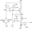
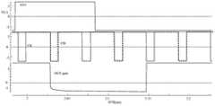
图1为一技术方案提供的像素驱动电路。如图1所示,该方案提供一种7T1C像素驱动电路,该像素驱动电路中,数据信号线Data的数据信号的电压驱动晶体管T03进行数据电压Vdata的写入及阈值电压Vth的补偿,晶体管T03的栅极的电压最终为Vdata+Vth。对于笔记本等较大尺寸的产品,Data电压写入的时间较短会造成Data电压写入不充分,产生斑块(mura)等不良现象。当频率由60赫兹(Hz)增加到120Hz时,栅极驱动信号的脉宽由6微秒(us)减小到现在的3us,同理当产品分辨率由QHD(Quarter High Definition,全高清分辨率的四分之一,960X540)提高到UHD(Ultra High Definition,超高清),栅极驱动信号的脉宽会再次减小一半。然而大尺寸产品的存储电容Cst无法减小,因而充电不足的现象会愈发严重。FIG. 1 is a pixel driving circuit provided by a technical solution. As shown in FIG. 1 , the solution provides a 7T1C pixel driving circuit. In the pixel driving circuit, the voltage driving transistor T03 of the data signal of the data signal line Data performs the writing of the data voltage Vdata and the compensation of the threshold voltage Vth, and the transistor T03 The voltage of the gate of is finally Vdata+Vth. For larger-sized products such as notebooks, the short writing time of the Data voltage will cause insufficient writing of the Data voltage, resulting in undesirable phenomena such as mura. When the frequency is increased from 60 Hz (Hz) to 120 Hz, the pulse width of the gate drive signal is reduced from 6 microseconds (us) to 3 us now. Similarly, when the product resolution is changed from QHD (Quarter High Definition, full HD resolution) 1/4, 960X540) to UHD (Ultra High Definition), the pulse width of the gate drive signal will be reduced by half again. However, the storage capacitance Cst of large-sized products cannot be reduced, so the phenomenon of insufficient charging will become more and more serious.
屏幕的亮度可以反映出像素Cst充电率的实际程度,如图2所示,充电时间在4us以后屏幕的亮度趋于稳定,表明在4us的时间内Cst的电压趋于稳定,充电率较高。然后当频率提高1倍或者分辨率提高1倍,充电时间会由目前的6us(QHD 60Hz NB产品)缩短到3us,这样造成充电率不足,一方面会引起像素(Pixel)之间的亮度差异,造成mura;另一方面会造成低灰阶漏光(低灰阶亮度较高),画面对比度降低。图3为充电率不足以及不均匀引起的mura问题示意图。如图3所示,在60Hz充电率不均匀mura程度较高,而15Hz的充电时间是60Hz的4倍,mura程度极大降低。The brightness of the screen can reflect the actual degree of the charging rate of the pixel Cst. As shown in Figure 2, the brightness of the screen tends to be stable after the charging time is 4us, indicating that the voltage of Cst tends to be stable within 4us and the charging rate is high. Then, when the frequency is doubled or the resolution is doubled, the charging time will be shortened from the current 6us (QHD 60Hz NB product) to 3us, which will result in insufficient charging rate. On the one hand, it will cause the brightness difference between pixels. cause mura; on the other hand, it will cause low grayscale light leakage (low grayscale brightness is higher), and the picture contrast will be reduced. Figure 3 is a schematic diagram of the mura problem caused by insufficient charging rate and unevenness. As shown in Figure 3, the unevenness of the charging rate at 60Hz is relatively high, while the charging time at 15Hz is 4 times that of 60Hz, and the degree of mura is greatly reduced.
本申请实施例中,采用data写入和Vth补偿分开进行的电路结构,用VDD电压写入存储电容一端,既补偿了VDD的IR drop(IR压降)又补偿了Vth电压,保证了Vdata电压的快速写入,在提高刷新率的同时降低了mura(斑块)的风险。在另一实施例中,用不同的GOA控制数据电压写入的时间和Vth补偿的时间,可以灵活控制Vth补偿时间。另外,本申请实施例中,只需要一条数据信号线,可以降低bonding bump(粘接凸点)的数量,极大降低了集成电路(IC)的驱动要求。In the embodiment of this application, a circuit structure in which data writing and Vth compensation are performed separately is used, and the VDD voltage is used to write one end of the storage capacitor, which not only compensates the IR drop (IR drop) of VDD, but also compensates the Vth voltage, ensuring the Vdata voltage. fast writes, reducing the risk of mura (patch) while increasing the refresh rate. In another embodiment, different GOAs are used to control the data voltage writing time and the Vth compensation time, so that the Vth compensation time can be flexibly controlled. In addition, in the embodiment of the present application, only one data signal line is required, which can reduce the number of bonding bumps and greatly reduce the driving requirements of an integrated circuit (IC).
如图4所示,Data信号可以经过两种方式充到Cst上,一种是经过补偿晶体管(SW-TFT)直接到Cst上,该方式的充电速度较快,如图4中(a)图所示;另一种是经过驱动晶体管(drive TFT)和SW TFT,该过程会进行Vth的补偿,在后期栅极电压接近于Vdata+Vth时,电流较小,因而充电速度较慢,如图4中(b)图所示。图1所示的7T1C电路依靠Data端,driveTFT和SW TFT组成二极管电路,该方案充电速度慢。本申请示例性实施例中,将数据信号线提供的data电压直接充到存储电容上,且采用第一电源线VDD提供的电压驱动补偿Vth,从而保证快速充电。在另一实施例中,Vth补偿时间和data电压写入时间不同,在延长Vth补偿时间时,可以使用较小的Data写入时间,提高了产品的刷新率。As shown in Figure 4, the Data signal can be charged to Cst in two ways. One is to directly charge Cst through a compensation transistor (SW-TFT). This method has a faster charging speed, as shown in (a) in Figure 4. The other is through the drive transistor (drive TFT) and SW TFT. This process will perform Vth compensation. When the gate voltage is close to Vdata+Vth in the later stage, the current is smaller, so the charging speed is slower, as shown in the figure. 4 (b) as shown. The 7T1C circuit shown in Figure 1 relies on the Data terminal, driveTFT and SW TFT to form a diode circuit, and the charging speed of this scheme is slow. In the exemplary embodiment of the present application, the data voltage provided by the data signal line is directly charged to the storage capacitor, and the voltage provided by the first power line VDD is used to drive the compensation Vth, thereby ensuring fast charging. In another embodiment, the Vth compensation time is different from the data voltage writing time. When the Vth compensation time is extended, a shorter Data writing time can be used, which improves the refresh rate of the product.
图5为本申请实施例提供的像素驱动电路的示意图。如图5所示,本申请实施例提供的像素驱动电路包括:数据写入子电路、驱动子电路、电平保持子电路、存储子电路、补偿子电路、发光控制子电路和发光元件。FIG. 5 is a schematic diagram of a pixel driving circuit provided by an embodiment of the present application. As shown in FIG. 5 , the pixel driving circuit provided by the embodiment of the present application includes: a data writing subcircuit, a driving subcircuit, a level holding subcircuit, a storage subcircuit, a compensation subcircuit, a light emission control subcircuit, and a light emission element.
所述数据写入子电路,与数据信号线Data、第一扫描信号线Gate1和第二节点N2连接,设置成在所述第一扫描信号线Gate1的控制下将所述数据信号线Data上的电压Vdata写入到所述存储子电路;The data writing subcircuit is connected to the data signal line Data, the first scanning signal line Gate1 and the second node N2, and is configured to write the data on the data signal line Data under the control of the first scanning signal line Gate1. The voltage Vdata is written to the storage sub-circuit;
所述驱动子电路,与第一电源线VDD、第一节点N1和第三节点N3连接,设置为在所述第一节点N1的控制下,通过所述第三节点N3向所述发光控制子电路输出驱动电流;The driving sub-circuit is connected to the first power supply line VDD, the first node N1 and the third node N3, and is configured to transmit to the light-emitting control sub-circuit through the third node N3 under the control of the first node N1. Circuit output drive current;
所述存储子电路,与所述第一节点N1和所述第二节点N2连接,设置为存储电压;the storage sub-circuit is connected to the first node N1 and the second node N2, and is set to a storage voltage;
所述电平保持子电路,与所述第一电源线VDD和所述第二节点N2连接,设置为保持所述第二节点N2的电平;the level maintaining sub-circuit is connected to the first power line VDD and the second node N2, and is set to maintain the level of the second node N2;
所述补偿子电路,与第二扫描信号线Gate2、所述第一节点N1和所述第三节点N3连接,设置为在所述第二扫描信号线Gate2的控制下,对所述驱动子电路的阈值电压Vth进行补偿;The compensation sub-circuit is connected to the second scan signal line Gate2, the first node N1 and the third node N3, and is configured to drive the sub-circuit under the control of the second scan signal line Gate2 The threshold voltage Vth is compensated;
所述发光控制子电路,与发光控制信号线EM、所述第三节点N3和所述发光元件的第一极连接;设置为在所述发光控制信号线EM的控制下,根据接收的驱动电流驱动所述发光元件发光;比如,在发光控制信号线EM的控制下,控制第三节点N3和发光元件的第一极之间导通或者断开。The light-emitting control sub-circuit is connected to the light-emitting control signal line EM, the third node N3 and the first pole of the light-emitting element; and is set to be controlled by the light-emitting control signal line EM according to the received driving current The light-emitting element is driven to emit light; for example, under the control of the light-emitting control signal line EM, the connection between the third node N3 and the first pole of the light-emitting element is controlled to be turned on or off.
所述发光元件的第二极与第二电源线VSS连接。The second pole of the light-emitting element is connected to the second power supply line VSS.
在一实施例中,所述发光元件可以为有机发光二极管OLED,第一极可以是阳极,第二极可以是阴极。In one embodiment, the light emitting element may be an organic light emitting diode OLED, the first electrode may be an anode, and the second electrode may be a cathode.
在一实施例中,所述第一电源线VDD提供的电压信号比如为高电平,第二电源线VSS提供的电压信号比如为低电平。In an embodiment, the voltage signal provided by the first power supply line VDD is, for example, a high level, and the voltage signal provided by the second power supply line VSS is, for example, a low level.
本实施例提供的像素驱动电路,通过第一电源线VDD输入的信号补偿阈值电压Vth,将数据信号线Data的电压直接直接充到存储子电路,提高了充电速度,Data电压写入充分,减少mura不良,另外阈值补偿和Data电压写入分开,可以灵活控制阈值补偿时间,提高刷新率。In the pixel driving circuit provided in this embodiment, the threshold voltage Vth is compensated by the signal input from the first power line VDD, and the voltage of the data signal line Data is directly charged to the storage sub-circuit, which improves the charging speed, and the writing of the Data voltage is sufficient, reducing the The mura is not good, and the threshold compensation and Data voltage writing are separated, which can flexibly control the threshold compensation time and improve the refresh rate.
在一示例性实施例中,所述数据写入子电路时间将所述数据信号线上的电压写入到所述存储子电路的写入时间小于所述补偿子电路对所述驱动子电路的阈值电压进行补偿的补偿时间。数据本实施例中,增加对阈值电压Vth进行补偿的补偿时间,Vth补偿时间充足,可以降低mura的严重程度,提高良率,data电压写入的时间不同于Vth补偿时间,可以在保证Vth补偿的时间时,减少Data电压写入的时间,从而提高产品的刷新率,因此,可以应用在高分辨率的产品中。In an exemplary embodiment, the writing time of the data writing sub-circuit to write the voltage on the data signal line to the storage sub-circuit is shorter than the writing time of the compensation sub-circuit to the driving sub-circuit Compensation time for threshold voltage compensation. In this embodiment, the compensation time for compensating the threshold voltage Vth is increased. The Vth compensation time is sufficient, which can reduce the severity of mura and improve the yield. The data voltage writing time is different from the Vth compensation time, which can ensure Vth compensation. When the time of the data voltage is reduced, the refresh rate of the product is improved, so it can be used in high-resolution products.
图6为另一实施例提供的像素驱动电路的结构图。如图6所示,本实施例提供的像素驱动电路还可以包括第一初始化子电路,所述第一初始化子电路与所述第一节点N1、第一复位信号线Reset1和初始化信号线INIT连接,设置为在所述第一复位信号线Reset1的控制下,对所述第一节点N1进行初始化。FIG. 6 is a structural diagram of a pixel driving circuit provided by another embodiment. As shown in FIG. 6 , the pixel driving circuit provided in this embodiment may further include a first initialization sub-circuit, and the first initialization sub-circuit is connected to the first node N1 , the first reset signal line Reset1 and the initialization signal line INIT , set to initialize the first node N1 under the control of the first reset signal line Reset1.
在另一实施例中,如图6所示,所述像素驱动电路还可以包括第二初始化子电路,所述第二初始化子电路与所述第二节点N2、第二复位信号线Reset2和参考信号线REF连接,设置为在所述第二复位信号线Reset2的控制下,对所述第二节点N2进行初始化。In another embodiment, as shown in FIG. 6 , the pixel driving circuit may further include a second initialization sub-circuit, the second initialization sub-circuit is connected to the second node N2, the second reset signal line Reset2 and the reference The signal line REF is connected and set to initialize the second node N2 under the control of the second reset signal line Reset2.
在另一实施例中,如图6所示,所述像素驱动电路还可以包括第三初始化子电路,所述第三初始化子电路与所述发光元件的第一极、初始化信号线INIT和第三复位信号线Reset2(n+1)连接;设置为在所述第三复位信号线Reset2(n+1)的控制下,对所述发光元件进行初始化。显示基板包括阵列分布的多个像素,同一行的子像素使用相同的栅极驱动信号(栅极驱动信号包括第一扫描信号线、第二扫描信号线、第一复位信号线、第二复位信号线、第三复位信号线等输出的信号),对n行,第n行的第三复位信号线Reset2(n+1)比如为第n+1行的第二复位信号线Reset2。所述对发光元件初始化包括:导通所述第一极与所述初始化信号线INIT,将所述初始化信号线的初始化电压Vinit提供给所述第一极,可以消除发光控制子电路的漏电流,避免发光元件受到该漏电流的影响而在暗态下发光,提高了显示质量。在一示例性实施例中,所述初始化电压比如为零电压或负电压。In another embodiment, as shown in FIG. 6 , the pixel driving circuit may further include a third initialization sub-circuit, the third initialization sub-circuit is connected to the first pole of the light-emitting element, the initialization signal line INIT and the third initialization sub-circuit. The three reset signal lines Reset2(n+1) are connected; it is set to initialize the light-emitting element under the control of the third reset signal line Reset2(n+1). The display substrate includes a plurality of pixels distributed in an array, and the sub-pixels in the same row use the same gate drive signal (the gate drive signal includes a first scan signal line, a second scan signal line, a first reset signal line, and a second reset signal line. line, the third reset signal line, etc.), for n rows, the third reset signal line Reset2(n+1) of the nth row is, for example, the second reset signal line Reset2 of the n+1th row. The initializing the light-emitting element includes: turning on the first electrode and the initialization signal line INIT, and supplying the initialization voltage Vinit of the initialization signal line to the first electrode, which can eliminate the leakage current of the light-emitting control sub-circuit , preventing the light-emitting element from being affected by the leakage current and emitting light in a dark state, thereby improving the display quality. In an exemplary embodiment, the initialization voltage is, for example, a zero voltage or a negative voltage.
图7为又一实施例提供的像素驱动电路的结构图。如图7所示,所述像素驱动电路还可以包括第二初始化子电路,所述第二初始化子电路与所述第二节点N2、第一复位信号线Reset1、所述第二扫描信号线Gate2和参考信号线REF连接,设置为在所述第一复位信号线Reset1和所述第二扫描信号线Gate2的控制下,对所述第二节点N2进行初始化。FIG. 7 is a structural diagram of a pixel driving circuit provided by yet another embodiment. As shown in FIG. 7 , the pixel driving circuit may further include a second initialization sub-circuit, the second initialization sub-circuit is connected to the second node N2, the first reset signal line Reset1, and the second scan signal line Gate2 It is connected to the reference signal line REF, and is configured to initialize the second node N2 under the control of the first reset signal line Reset1 and the second scanning signal line Gate2.
在另一实施例中,如图7所示,所述像素驱动电路还可以包括第三初始化子电路,所述第三初始化子电路与所述发光元件的第一极、初始化信号线INIT和第二扫描信号线Gate2连接,设置为在所述第二扫描信号线Gate2的控制下,对所述发光元件进行初始化。In another embodiment, as shown in FIG. 7 , the pixel driving circuit may further include a third initialization sub-circuit, the third initialization sub-circuit is connected to the first pole of the light-emitting element, the initialization signal line INIT and the third initialization sub-circuit. The two scanning signal lines Gate2 are connected, and are configured to initialize the light-emitting element under the control of the second scanning signal line Gate2.
在一示例性实施例中,所述第三初始化子电路对所述发光元件进行初始化的初始化时间大于写入时间和补偿时间之和,所述写入时间为所述数据写入子电路时间将所述数据信号线上的电压写入到所述存储子电路的时长,所述补偿时间为所述补偿子电路对所述驱动子电路的阈值电压进行补偿的时长。OLED像素驱动电路对于OLED器件属于脉冲型供电,非连续性供电。对发光元件的第一极施加初始化电压,可以消除第一极表面残余正电荷,提高发光元件的寿命。图1所示方案中,当频率提升或分辨率增大,T07开启的时间减短,对发光元件第一极表面残余正电荷消除不彻底,降低了发光元件的寿命,使得面板的寿命低于预期。本实施例中,初始化时间大于写入时间和补偿时间之和,增加了初始化时间,对发光元件第一极表面残余正电荷消除较为彻底,提高了发光元件的寿命,即提高了面板的寿命。In an exemplary embodiment, the initialization time for the third initialization sub-circuit to initialize the light-emitting element is greater than the sum of the writing time and the compensation time, and the writing time is the time of the data writing sub-circuit The duration of writing the voltage on the data signal line to the storage sub-circuit, and the compensation time is the duration of the compensation sub-circuit to compensate the threshold voltage of the driving sub-circuit. The OLED pixel drive circuit belongs to the pulse type power supply for the OLED device, and the power supply is discontinuous. Applying an initialization voltage to the first electrode of the light-emitting element can eliminate the residual positive charges on the surface of the first electrode and improve the life of the light-emitting element. In the scheme shown in Figure 1, when the frequency is increased or the resolution is increased, the time for T07 to be turned on is shortened, and the residual positive charge on the surface of the first pole of the light-emitting element is not completely eliminated, which reduces the life of the light-emitting element, making the life of the panel less than expected. In this embodiment, the initialization time is greater than the sum of the writing time and the compensation time, which increases the initialization time, eliminates the residual positive charge on the surface of the first pole of the light-emitting element more completely, and improves the life of the light-emitting element, that is, the life of the panel.
图8为一实施例提供的驱动子电路示意图。如图8所示,本实施例提供的所述驱动子电路可以包括第三晶体管T3,所述第三晶体管T3的控制极连接所述第一节点N1,第一极连接所述第一电源线VDD,第二极连接所述第三节点N3。FIG. 8 is a schematic diagram of a driving sub-circuit provided by an embodiment. As shown in FIG. 8 , the driving sub-circuit provided in this embodiment may include a third transistor T3, a control electrode of the third transistor T3 is connected to the first node N1, and a first electrode is connected to the first power line VDD, the second pole is connected to the third node N3.
图9为一实施例提供的数据写入子电路示意图。如图9所示,所述数据写入子电路可以包括第四晶体管T4,所述第四晶体管T4的控制极连接所述第一扫描信号信号线Gate1,第一极连接所述数据信号线Data,第二极连接所述第二节点N2。FIG. 9 is a schematic diagram of a data writing sub-circuit according to an embodiment. As shown in FIG. 9 , the data writing sub-circuit may include a fourth transistor T4, the control electrode of the fourth transistor T4 is connected to the first scanning signal signal line Gate1, and the first electrode is connected to the data signal line Data , the second pole is connected to the second node N2.
图10为一实施例提供的存储子电路示意图。如图10所示,所述存储子电路可以包括第一电容C1,所述第一电容C1的第一端连接所述第一节点N1,第二端连接所述第二节点N2。FIG. 10 is a schematic diagram of a storage sub-circuit according to an embodiment. As shown in FIG. 10 , the storage sub-circuit may include a first capacitor C1, a first end of the first capacitor C1 is connected to the first node N1, and a second end of the first capacitor C1 is connected to the second node N2.
图11为一实施例提供的电平保持子电路示意图。如图11所示,所述电平保持子电路可以包括第二电容C2,所述第二电容C2的第一端连接所述第一电源线VDD,第二端连接所述第二节点N2。FIG. 11 is a schematic diagram of a level-holding sub-circuit provided by an embodiment. As shown in FIG. 11 , the level-holding sub-circuit may include a second capacitor C2, a first end of the second capacitor C2 is connected to the first power supply line VDD, and a second end of the second capacitor C2 is connected to the second node N2.
图12为一实施例提供的电平保持子电路示意图。如图12所示,所述补偿子电路可以包括第二晶体管T2,所述第二晶体管T2的控制极连接所述第二扫描信号线Gate2,第一极连接所述第三节点N3,第二极连接所述第一节点N1。FIG. 12 is a schematic diagram of a level-holding sub-circuit provided by an embodiment. As shown in FIG. 12 , the compensation sub-circuit may include a second transistor T2, a control electrode of the second transistor T2 is connected to the second scan signal line Gate2, a first electrode is connected to the third node N3, and a second transistor T2 is connected to the second scan signal line Gate2. The pole is connected to the first node N1.
图13为一实施例提供的发光控制子电路示意图。如图13所示,所述发光控制子电路可以包括第六晶体管T6,所述第六晶体管T6的控制极连接所述发光控制信号线EM,第一极连接第三节点N3,第二极连接所述发光元件的第一极。FIG. 13 is a schematic diagram of a lighting control sub-circuit according to an embodiment. As shown in FIG. 13 , the light-emitting control sub-circuit may include a sixth transistor T6, the control electrode of the sixth transistor T6 is connected to the light-emitting control signal line EM, the first electrode is connected to the third node N3, and the second electrode is connected to the third node N3. the first pole of the light-emitting element.
图14为一实施例提供的第一初始化子电路示意图。如图14所示,所述第一初始化子电路可以包括第一晶体管T1,所述第一晶体管T1的控制极连接所述第一复位信号线Reset1,第一极连接所述初始化信号线INIT,第二极连接所述第一节点N1。FIG. 14 is a schematic diagram of a first initialization sub-circuit according to an embodiment. As shown in FIG. 14 , the first initialization sub-circuit may include a first transistor T1, the control electrode of the first transistor T1 is connected to the first reset signal line Reset1, and the first electrode is connected to the initialization signal line INIT, The second pole is connected to the first node N1.
图15为一实施例提供的第二初始化子电路示意图。如图15所示,所述第二初始化子电路可以包括第五晶体管T5,所述第五晶体管T5的控制极连接所述第二复位信号线Reset2,第一极连接所述参考信号线REF,第二极连接所述第二节点N2。FIG. 15 is a schematic diagram of a second initialization sub-circuit according to an embodiment. As shown in FIG. 15 , the second initialization sub-circuit may include a fifth transistor T5, the control electrode of the fifth transistor T5 is connected to the second reset signal line Reset2, the first electrode is connected to the reference signal line REF, The second pole is connected to the second node N2.
图16为一实施例提供的第三初始化子电路示意图。如图16所示,所述第三初始化子电路可以包括第七晶体管T7,所述第七晶体管T7的控制极连接第三复位信号线Reste2(n+1),第一极连接初始化信号线INIT,第二极连接所述发光元件的第一极。FIG. 16 is a schematic diagram of a third initialization sub-circuit according to an embodiment. As shown in FIG. 16 , the third initialization sub-circuit may include a seventh transistor T7, the control electrode of the seventh transistor T7 is connected to the third reset signal line Reste2(n+1), and the first electrode is connected to the initialization signal line INIT , the second pole is connected to the first pole of the light-emitting element.
图17为一实施例提供的第二初始化子电路示意图。如图17所示,所述第二初始化子电路可以包括第八晶体管T8和第九晶体管T9,所述第八晶体管T8的控制极连接第一复位信号线Reset1,第一极连接参考信号线REF,第二极连接第二节点N2;所述第九晶体管T9的控制极连接第二扫描信号线Gate2,第一极连接参考信号线REF,第二极连接第二节点N2。FIG. 17 is a schematic diagram of a second initialization sub-circuit according to an embodiment. As shown in FIG. 17 , the second initialization sub-circuit may include an eighth transistor T8 and a ninth transistor T9, the control electrode of the eighth transistor T8 is connected to the first reset signal line Reset1, and the first electrode is connected to the reference signal line REF , the second electrode is connected to the second node N2; the control electrode of the ninth transistor T9 is connected to the second scanning signal line Gate2, the first electrode is connected to the reference signal line REF, and the second electrode is connected to the second node N2.
图18为一实施例提供的第三初始化子电路示意图。如图16所示,所述第三初始化子电路可以包括第七晶体管T7,所述第七晶体管T7的控制极连接第二扫描信号线,第一极连接初始化信号线INIT,第二极连接所述发光元件的第一极。FIG. 18 is a schematic diagram of a third initialization sub-circuit according to an embodiment. As shown in FIG. 16 , the third initialization sub-circuit may include a seventh transistor T7, the control electrode of the seventh transistor T7 is connected to the second scan signal line, the first electrode is connected to the initialization signal line INIT, and the second electrode is connected to the second scan signal line. the first pole of the light-emitting element.
图8至图18示出了多个子电路的示例性结构,本领域技术人员容易理解的是,上述多个子电路的实现方式并不限于此,只要能够实现其功能即可。FIG. 8 to FIG. 18 show exemplary structures of multiple sub-circuits, and those skilled in the art can easily understand that the implementation manner of the above-mentioned multiple sub-circuits is not limited to this, as long as its functions can be realized.
图19为一实施例提供的像素驱动电路的一个等效电路图。如图19所示,所述像素驱动电路可以包括:驱动子电路、数据写入子电路、存储子电路、电平保持子电路、补偿子电路、发光控制子电路和发光元件,所述发光元件比如为有机发光二极管OLED,其中:FIG. 19 is an equivalent circuit diagram of a pixel driving circuit provided by an embodiment. As shown in FIG. 19 , the pixel driving circuit may include: a driving sub-circuit, a data writing sub-circuit, a storage sub-circuit, a level-holding sub-circuit, a compensation sub-circuit, a light-emitting control sub-circuit, and a light-emitting element, the light-emitting element For example, an organic light-emitting diode OLED, in which:
所述驱动子电路可以包括第三晶体管T3,所述第三晶体管T3的控制极连接所述第一节点N1,第一极连接所述第一电源线VDD,第二极连接所述第三节点N3;The driving sub-circuit may include a third transistor T3, a control electrode of the third transistor T3 is connected to the first node N1, a first electrode is connected to the first power supply line VDD, and a second electrode is connected to the third node N3;
所述数据写入子电路可以包括第四晶体管T4,所述第四晶体管T4的控制极连接所述第一扫描信号线Gate1,第一极连接所述数据信号线Data,第二极连接所述第二节点N2;The data writing sub-circuit may include a fourth transistor T4, the control electrode of the fourth transistor T4 is connected to the first scan signal line Gate1, the first electrode is connected to the data signal line Data, and the second electrode is connected to the the second node N2;
所述存储子电路可以包括第一电容C1,所述第一电容C1的第一端连接所述第一节点N1,第二端连接所述第二节点N2;The storage sub-circuit may include a first capacitor C1, a first end of the first capacitor C1 is connected to the first node N1, and a second end is connected to the second node N2;
所述电平保持子电路可以包括第二电容C2,所述第二电容C2的第一端连接所述第一电源线VDD,第二端连接所述第二节点N2;第二电容C2起到稳定第一电容C1电位的作用,不参与补偿子电路,因而避免了工艺误差对电路稳定性的影响。The level-holding sub-circuit may include a second capacitor C2, the first end of the second capacitor C2 is connected to the first power supply line VDD, and the second end is connected to the second node N2; the second capacitor C2 serves to The function of stabilizing the potential of the first capacitor C1 does not participate in the compensation sub-circuit, thus avoiding the influence of the process error on the stability of the circuit.
所述补偿子电路可以包括第二晶体管T2,所述第二晶体管T2的控制极连接所述第二扫描信号线Gate2,第一极连接所述第三节点N3,第二极连接所述第一节点N1;The compensation sub-circuit may include a second transistor T2, a control electrode of the second transistor T2 is connected to the second scan signal line Gate2, a first electrode is connected to the third node N3, and a second electrode is connected to the first node N1;
所述发光控制子电路可以包括第六晶体管T6,所述第六晶体管T6的控制极连接所述发光控制信号线EM,第一极连接第三节点N3,第二极连接所述发光元件的第一极;第六晶体管T6导通时,导通第三节点N3和有机发光二极管OLED的第一极,从而可以控制OLED的发光时间段。The light-emitting control sub-circuit may include a sixth transistor T6, the control electrode of the sixth transistor T6 is connected to the light-emitting control signal line EM, the first electrode is connected to the third node N3, and the second electrode is connected to the first electrode of the light-emitting element. One pole; when the sixth transistor T6 is turned on, the third node N3 and the first pole of the organic light emitting diode OLED are turned on, so that the light-emitting period of the OLED can be controlled.
所述有机发光二极管OLED的第二极连接第二电源端VSS。The second pole of the organic light emitting diode OLED is connected to the second power supply terminal VSS.
图20为一实施例提供的像素驱动电路的结构图。本实施例提供的像素驱动电路为7T2C结构。如图20所示,所述像素驱动电路可以包括驱动子电路、数据写入子电路、存储子电路、电平保持子电路、补偿子电路、发光控制子电路、第一初始化子电路、第二初始化子电路、第三初始化子电路和发光元件,所述发光元件比如为有机发光二极管OLED,其中:FIG. 20 is a structural diagram of a pixel driving circuit according to an embodiment. The pixel driving circuit provided in this embodiment has a 7T2C structure. As shown in FIG. 20 , the pixel driving circuit may include a driving sub-circuit, a data writing sub-circuit, a storage sub-circuit, a level-holding sub-circuit, a compensation sub-circuit, a lighting control sub-circuit, a first initialization sub-circuit, a second sub-circuit an initialization subcircuit, a third initialization subcircuit, and a light-emitting element, such as an organic light-emitting diode OLED, wherein:
所述驱动子电路可以包括第三晶体管T3,所述第三晶体管T3的控制极连接所述第一节点N1,第一极连接所述第一电源线VDD,第二极连接所述第三节点N3;The driving sub-circuit may include a third transistor T3, a control electrode of the third transistor T3 is connected to the first node N1, a first electrode is connected to the first power supply line VDD, and a second electrode is connected to the third node N3;
所述数据写入子电路可以包括第四晶体管T4,所述第四晶体管T4的控制极连接所述第一扫描信号线Gate1,第一极连接所述数据信号线Data,第二极连接所述第二节点N2;The data writing sub-circuit may include a fourth transistor T4, the control electrode of the fourth transistor T4 is connected to the first scan signal line Gate1, the first electrode is connected to the data signal line Data, and the second electrode is connected to the the second node N2;
所述存储子电路可以包括第一电容C1,所述第一电容C1的第一端连接所述第一节点N1,第二端连接所述第二节点N2;The storage sub-circuit may include a first capacitor C1, a first end of the first capacitor C1 is connected to the first node N1, and a second end is connected to the second node N2;
所述电平保持子电路可以包括第二电容C2,所述第二电容C2的第一端连接所述第一电源线VDD,第二端连接所述第二节点N2;第二电容C2起到稳定第一电容C1电位的作用,不参与补偿子电路,因而避免了工艺误差对电路稳定性的影响。The level-holding sub-circuit may include a second capacitor C2, the first end of the second capacitor C2 is connected to the first power supply line VDD, and the second end is connected to the second node N2; the second capacitor C2 serves to The function of stabilizing the potential of the first capacitor C1 does not participate in the compensation sub-circuit, thus avoiding the influence of the process error on the stability of the circuit.
所述补偿子电路可以包括第二晶体管T2,所述第二晶体管T2的控制极连接所述第二扫描信号线Gate2,第一极连接所述第三节点N3,第二极连接所述第一节点N1;The compensation sub-circuit may include a second transistor T2, a control electrode of the second transistor T2 is connected to the second scan signal line Gate2, a first electrode is connected to the third node N3, and a second electrode is connected to the first node N1;
所述发光控制子电路可以包括第六晶体管T6,所述第六晶体管T6的控制极连接所述发光控制信号线EM,第一极连接第三节点N3,第二极连接所述发光元件的第一极;第六晶体管T6导通时,导通第三节点N3和有机发光二极管OLED的第一极,从而可以控制OLED的发光时间段。The light-emitting control sub-circuit may include a sixth transistor T6, the control electrode of the sixth transistor T6 is connected to the light-emitting control signal line EM, the first electrode is connected to the third node N3, and the second electrode is connected to the first electrode of the light-emitting element. One pole; when the sixth transistor T6 is turned on, the third node N3 and the first pole of the organic light emitting diode OLED are turned on, so that the light-emitting period of the OLED can be controlled.
所述第一初始化子电路可以包括第一晶体管T1,所述第一晶体管T1的控制极连接所述第一复位信号线Reset1,第一极连接所述初始化信号线INIT,第二极连接所述第一节点N1;第一晶体管T1导通时,将初始化信号线INIT的初始化电压Vinit提供给第一节点N1,对第一电容C1进行复位;The first initialization sub-circuit may include a first transistor T1, a control electrode of the first transistor T1 is connected to the first reset signal line Reset1, a first electrode is connected to the initialization signal line INIT, and a second electrode is connected to the The first node N1; when the first transistor T1 is turned on, the initialization voltage Vinit of the initialization signal line INIT is provided to the first node N1, and the first capacitor C1 is reset;
所述第二初始化子电路可以包括第五晶体管T5,所述第五晶体管T5的控制极连接所述第二复位信号线Reset2,第一极连接所述参考信号线REF,第二极连接所述第二节点N2;第五晶体管T5导通时,将参考信号线REF的参考电压Vref提供给第二节点N2,对第一电容C1进行复位;The second initialization sub-circuit may include a fifth transistor T5, a control electrode of the fifth transistor T5 is connected to the second reset signal line Reset2, a first electrode is connected to the reference signal line REF, and a second electrode is connected to the the second node N2; when the fifth transistor T5 is turned on, the reference voltage Vref of the reference signal line REF is provided to the second node N2, and the first capacitor C1 is reset;
所述第三初始化子电路可以包括第七晶体管T7,所述第七晶体管T7的控制极连接第三复位信号线Reset2(n+1),第一极连接初始化信号线INIT,第二极连接所述发光元件的第一极。The third initialization sub-circuit may include a seventh transistor T7, the control electrode of the seventh transistor T7 is connected to the third reset signal line Reset2(n+1), the first electrode is connected to the initialization signal line INIT, and the second electrode is connected to the third reset signal line Reset2(n+1). the first pole of the light-emitting element.
所述有机发光二极管OLED的第二极连接第二电源端VSS。The second pole of the organic light emitting diode OLED is connected to the second power supply terminal VSS.
图21为一实施例提供的像素驱动电路的结构图。如图21所示,所述像素驱动电路可以包括驱动子电路、数据写入子电路、存储子电路、电平保持子电路、补偿子电路、发光控制子电路、第一初始化子电路、第二初始化子电路、第三初始化子电路和发光元件,所述发光元件比如为有机发光二极管OLED,其中:FIG. 21 is a structural diagram of a pixel driving circuit provided by an embodiment. As shown in FIG. 21 , the pixel driving circuit may include a driving sub-circuit, a data writing sub-circuit, a storage sub-circuit, a level-holding sub-circuit, a compensation sub-circuit, a lighting control sub-circuit, a first initialization sub-circuit, a second sub-circuit an initialization subcircuit, a third initialization subcircuit, and a light-emitting element, such as an organic light-emitting diode OLED, wherein:
所述驱动子电路可以包括第三晶体管T3,所述第三晶体管T3的控制极连接所述第一节点N1,第一极连接所述第一电源线VDD,第二极连接所述第三节点N3;The driving sub-circuit may include a third transistor T3, a control electrode of the third transistor T3 is connected to the first node N1, a first electrode is connected to the first power supply line VDD, and a second electrode is connected to the third node N3;
所述数据写入子电路可以包括第四晶体管T4,所述第四晶体管T4的控制极连接所述第一扫描信号线Gate1,第一极连接所述数据信号线Data,第二极连接所述第二节点N2;The data writing sub-circuit may include a fourth transistor T4, the control electrode of the fourth transistor T4 is connected to the first scan signal line Gate1, the first electrode is connected to the data signal line Data, and the second electrode is connected to the the second node N2;
所述存储子电路可以包括第一电容C1,所述第一电容C1的第一端连接所述第一节点N1,第二端连接所述第二节点N2;The storage sub-circuit may include a first capacitor C1, a first end of the first capacitor C1 is connected to the first node N1, and a second end is connected to the second node N2;
所述电平保持子电路可以包括第二电容C2,所述第二电容C2的第一端连接所述第一电源线VDD,第二端连接所述第二节点N2;The level maintaining sub-circuit may include a second capacitor C2, a first end of the second capacitor C2 is connected to the first power supply line VDD, and a second end is connected to the second node N2;
所述补偿子电路可以包括第二晶体管T2,所述第二晶体管T2的控制极连接所述第二扫描信号线Gate2,第一极连接所述第三节点N3,第二极连接所述第一节点N1;The compensation sub-circuit may include a second transistor T2, a control electrode of the second transistor T2 is connected to the second scan signal line Gate2, a first electrode is connected to the third node N3, and a second electrode is connected to the first node N1;
所述发光控制子电路可以包括第六晶体管T6,所述第六晶体管T6的控制极连接所述发光控制信号线EM,第一极连接第三节点N3,第二极连接所述发光元件的第一极;The light-emitting control sub-circuit may include a sixth transistor T6, the control electrode of the sixth transistor T6 is connected to the light-emitting control signal line EM, the first electrode is connected to the third node N3, and the second electrode is connected to the first electrode of the light-emitting element. one pole
所述第一初始化子电路可以包括第一晶体管T1,所述第一晶体管T1的控制极连接所述第一复位信号线Reset1,第一极连接所述初始化信号线INIT,第二极连接所述第一节点N1;The first initialization sub-circuit may include a first transistor T1, a control electrode of the first transistor T1 is connected to the first reset signal line Reset1, a first electrode is connected to the initialization signal line INIT, and a second electrode is connected to the the first node N1;
所述第二初始化子电路可以包括第八晶体管T8和第九晶体管T9,所述第八晶体管T8的控制极连接第一复位信号线Reset1,第一极连接参考信号线REF,第二极连接第二节点N2;所述第九晶体管T9的控制极连接第二扫描信号线Gate2,第一极连接参考信号线REF,第二极连接第二节点N2;The second initialization sub-circuit may include an eighth transistor T8 and a ninth transistor T9. The control electrode of the eighth transistor T8 is connected to the first reset signal line Reset1, the first electrode is connected to the reference signal line REF, and the second electrode is connected to the first reset signal line. Two nodes N2; the control electrode of the ninth transistor T9 is connected to the second scanning signal line Gate2, the first electrode is connected to the reference signal line REF, and the second electrode is connected to the second node N2;
所述第三初始化子电路可以包括第七晶体管T7,所述第七晶体管T7的控制极连接第二扫描信号线Gate2,第一极连接初始化信号线INIT,第二极连接所述发光元件的第一极;The third initialization sub-circuit may include a seventh transistor T7, the control electrode of the seventh transistor T7 is connected to the second scanning signal line Gate2, the first electrode is connected to the initialization signal line INIT, and the second electrode is connected to the first electrode of the light-emitting element. one pole
所述有机发光二极管OLED的第二极连接第二电源端VSS。The second pole of the organic light emitting diode OLED is connected to the second power supply terminal VSS.
本实施例提供的像素驱动电路,相比图20中的像素驱动电路,增加了一个TFT,减少了栅极驱动信号(栅极驱动信号线包括第一扫描信号线Gate1,第二扫描信号线Gate2,第一复位信号线Reset1,发光控制信号线EM提供的信号,不需要第二复位信号线Reset2),可以缩减边框,实现窄边框,应用在窄边框产品中。Compared with the pixel driving circuit in FIG. 20, the pixel driving circuit provided in this embodiment adds one TFT and reduces the gate driving signal (the gate driving signal line includes the first scanning signal line Gate1, the second scanning signal line Gate2 , the first reset signal line Reset1, the signal provided by the light-emitting control signal line EM does not need the second reset signal line Reset2), which can reduce the frame, realize a narrow frame, and be applied in narrow frame products.
下面通过一示例说明像素驱动电路的工作过程。本实施例的像素驱动电路如图20所示。以第一晶体管T1至第七晶体管T7为P型晶体管为例进行说明。图22为本实施例提供的像素驱动电路的工作时序图;图23为像素驱动电路在复位阶段的工作状态图,图24为像素驱动电路在补偿阶段的工作状态图,图25为像素驱动电路在写入阶段的工作状态图,图26为像素驱动电路在发光阶段的工作状态图。The working process of the pixel driving circuit is described below through an example. The pixel driving circuit of this embodiment is shown in FIG. 20 . The first to seventh transistors T1 to T7 are P-type transistors as an example for description. FIG. 22 is a working timing diagram of the pixel driving circuit provided by this embodiment; FIG. 23 is a working state diagram of the pixel driving circuit in the reset stage, FIG. 24 is a working state diagram of the pixel driving circuit in the compensation stage, and FIG. 25 is the pixel driving circuit. The working state diagram in the writing stage, FIG. 26 is the working state diagram of the pixel driving circuit in the light-emitting stage.
第一阶段t1,即复位阶段,第一复位信号线Reset1提供低电平信号,第一晶体管T1开启,第一节点N1的电压VN1为初始化信号线INIT提供的初始化电压Vinit,第二复位信号线Reset2提供低电平信号,第五晶体管T5开启(即导通),第二节点N2的电压为参考信号线REF提供的电压Vref,第一电容C1复位,清除第一电容C1中原有数据电压;第一扫描信号线Gate1提供高电平信号和第二扫描信号线Gate2提供高电平信号,第四晶体管T4和第二晶体管T2关断,发光控制信号线EM提供高电平信号,第六晶体管T6关断,第三晶体管T3的控制极电压为初始化信号线INIT提供的电压Vinit,第二节点N2的电压为参考信号线REF提供的电压Vref。数据信号线Data提供低电平信号。如图23所示。In the first stage t1, the reset stage, the first reset signal line Reset1 provides a low level signal, the first transistor T1 is turned on, the voltage VN1 of the first node N1 is the initialization voltage Vinit provided by the initialization signal line INIT, and the second reset signal Line Reset2 provides a low-level signal, the fifth transistor T5 is turned on (ie, turned on), the voltage of the second node N2 is the voltage Vref provided by the reference signal line REF, the first capacitor C1 is reset, and the original data voltage in the first capacitor C1 is cleared. ; The first scanning signal line Gate1 provides a high-level signal and the second scanning signal line Gate2 provides a high-level signal, the fourth transistor T4 and the second transistor T2 are turned off, the light-emitting control signal line EM provides a high-level signal, and the sixth The transistor T6 is turned off, the gate voltage of the third transistor T3 is the voltage Vinit provided by the initialization signal line INIT, and the voltage of the second node N2 is the voltage Vref provided by the reference signal line REF. The data signal line Data provides a low level signal. As shown in Figure 23.
第二阶段t2,即补偿阶段,第一复位信号线Reset1提供高电平信号,第一晶体管T1关断。第二复位信号线Reset2提供低电平信号,第五晶体管T5开启,第二节点N2的电压仍为Vref。第二扫描信号线Gate2提供低电平信号,第二晶体管T2开启。第一扫描信号信号线Gate1提供高电平信号,第四晶体管T4关断。发光控制信号线EM提供高电平信号,第六晶体管T6关断。第三复位信号Reset2(n+1)提供低电平信号,第七晶体管T7开启,将初始化信号线INIT的电压提供给发光元件的第一极,对发光元件的第一极进行初始化。数据信号线Data提供低电平信号。在第二阶段t2开始时,第一电源线VDD提供的电压VVDD与第一节点N1(在第一阶段t1中,第一节点N1的电压为Vinit)的电压差大于第三晶体管T3的阈值电压Vth,此时第三晶体管T3导通,第一电源端VDD的电压经过第三晶体管T3和第二晶体管T2流入第一节点N1,由于第二晶体管T2打开时间比较长,最终第三晶体管T3的Vth可以得到充分的补偿,当第一节点N1的电压升高到VVDD+Vth时,第三晶体管T3截止,此时第一节点N1的电压为VVDD+Vth,第二节点N2的电压为Vref,第一节点N1和第二节点N2的电压差为VVDD+Vth-Vref;如图24所示。In the second stage t2, that is, the compensation stage, the first reset signal line Reset1 provides a high level signal, and the first transistor T1 is turned off. The second reset signal line Reset2 provides a low level signal, the fifth transistor T5 is turned on, and the voltage of the second node N2 is still Vref. The second scan signal line Gate2 provides a low level signal, and the second transistor T2 is turned on. The first scan signal line Gate1 provides a high level signal, and the fourth transistor T4 is turned off. The light-emitting control signal line EM provides a high-level signal, and the sixth transistor T6 is turned off. The third reset signal Reset2(n+1) provides a low level signal, the seventh transistor T7 is turned on, and the voltage of the initialization signal line INIT is supplied to the first electrode of the light-emitting element to initialize the first electrode of the light-emitting element. The data signal line Data provides a low level signal. At the beginning of the second stage t2, the voltage difference between the voltage VVDD provided by the first power supply line VDD and the first node N1 (in the first stage t1, the voltage of the first node N1 is Vinit) is greater than the threshold of the third transistor T3 At this time, the third transistorT3 is turned on, and the voltage of the first power supply terminal VDD flows into the first node N1 through the third transistor T3 and the second transistor T2. Because the second transistor T2 is turned on for a long time, finally the third transistor T2 is turned on for a long time. The Vth of T3 can be fully compensated. When the voltage of the first node N1 rises to VVDD +Vth, the third transistor T3 is turned off. At this time, the voltage of the first node N1 is VVDD +Vth, and the voltage of the second node N2 is V VDD +Vth. The voltage is Vref, and the voltage difference between the first node N1 and the second node N2 is VVDD +Vth-Vref; as shown in FIG. 24 .
第三阶段t3,即写入阶段,第一复位信号线Reset1提供高电平信号,第一晶体管T1关断,第二扫描信号线Gate2提供高电平信号,第二晶体管T2关断,第二复位信号线Reset2提供高电平信号,第五晶体管T5关断,发光控制信号线EM提供高电平信号,第六晶体管T6关断,数据信号线Data提供高电平信号Vdata,第一扫描信号线Gate1提供低电平信号,第四晶体管T4开启,数据信号线Data提供的信号写入到第二节点N2,即第二节点N2的电压变为Vdata,第一电容C1会产生自举效应以维持第一电容C1两端电压差不变,则第一节点N1的电位由于电容自举的原理最终电压变为VVDD+Vth+Vdata-Vref,维持第一节点N1和第二节点N2的电压差为VVDD+Vth+Vdata-Vref-Vdata=VVDD+Vth-Vref。如图25所示。本实施例中,数据信号线Data的电压的写入是单电容充电方式,与第一电容C1和第二电容C2的电容值比例无关,因此,即使第一电容C1和第二电容C2的电容值比例出现偏差,也不影响数据信号线Data的电压的写入,因此,本实施例提供的方案,由工艺波动引起的mura风险小。另外,C1和C2无固定比例,降低了工艺要求。The third stage t3, the writing stage, the first reset signal line Reset1 provides a high level signal, the first transistor T1 is turned off, the second scan signal line Gate2 provides a high level signal, the second transistor T2 is turned off, the second The reset signal line Reset2 provides a high-level signal, the fifth transistor T5 is turned off, the light-emitting control signal line EM provides a high-level signal, the sixth transistor T6 is turned off, the data signal line Data provides a high-level signal Vdata, and the first scan signal The line Gate1 provides a low-level signal, the fourth transistor T4 is turned on, and the signal provided by the data signal line Data is written to the second node N2, that is, the voltage of the second node N2 becomes Vdata, and the first capacitor C1 will generate a bootstrap effect to Keeping the voltage difference between the two ends of the first capacitor C1 unchanged, the potential of the first node N1 becomes VVDD +Vth+Vdata-Vref due to the principle of capacitor bootstrapping, and the voltages of the first node N1 and the second node N2 are maintained. The difference is VVDD + Vth + Vdata - Vref - Vdata = VVDD + Vth - Vref. As shown in Figure 25. In this embodiment, the voltage of the data signal line Data is written in a single-capacitor charging method, which has nothing to do with the capacitance ratio of the first capacitor C1 and the second capacitor C2. Therefore, even if the capacitances of the first capacitor C1 and the second capacitor C2 The deviation of the value ratio does not affect the writing of the voltage of the data signal line Data. Therefore, the solution provided by this embodiment has little mura risk caused by process fluctuations. In addition, there is no fixed ratio of C1 and C2, which reduces the process requirements.
第四阶段t4,即发光阶段,第一复位信号线Reset1提供高电平信号,第一晶体管T1关断,第二扫描信号线Gate2提供高电平信号,第二晶体管T2关断,第一扫描信号线Gate1提供高电平信号,第四晶体管T4关断,第二复位信号线Reset2提供高电平信号,第五晶体管T5关断,发光控制信号线EM提供低电平信号,第六晶体管T6开启,数据信号线Data提供低电平信号,第一电源端VDD和第一节点N1的电压差Vth+Vdata-Vref大于第三晶体管T3的阈值电压Vth,此时第三晶体管T3开启,发光元件(本实施例中为有机发光二极管OLED)在第三晶体管T3的驱动下发光。如图26所示。最终OLED的发光电流为:The fourth stage t4, that is, the light-emitting stage, the first reset signal line Reset1 provides a high-level signal, the first transistor T1 is turned off, the second scanning signal line Gate2 provides a high-level signal, the second transistor T2 is turned off, and the first scan The signal line Gate1 provides a high-level signal, the fourth transistor T4 is turned off, the second reset signal line Reset2 provides a high-level signal, the fifth transistor T5 is turned off, the light-emitting control signal line EM provides a low-level signal, and the sixth transistor T6 Turn on, the data signal line Data provides a low level signal, the voltage difference Vth+Vdata-Vref between the first power supply terminal VDD and the first node N1 is greater than the threshold voltage Vth of the third transistor T3, at this time the third transistor T3 is turned on, the light-emitting element (The organic light emitting diode OLED in this embodiment) emits light under the driving of the third transistor T3. As shown in Figure 26. The luminous current of the final OLED is:


其中,u,W,L为与第三晶体管T3的工艺参数和几何尺寸有关的固定常数,Vgs为第三晶体管T3的栅源电压差,Vth为第三晶体管T3的阈值电压。可以看到,上述电流I与VDD和Vth无关,只取决于数据信号线Data提供的电压Vdata和参考信号线REF提供的电压Vref,从而消除了第三晶体管T3的阈值电压对驱动电流的影响,进而确保了显示装置的显示亮度均匀,提高了整个显示装置的显示效果。Wherein, u, W, L are fixed constants related to process parameters and geometric dimensions of the third transistor T3, Vgs is the gate-source voltage difference of the third transistor T3, and Vth is the threshold voltage of the third transistor T3. It can be seen that the above current I has nothing to do with VDD and Vth, but only depends on the voltage Vdata provided by the data signal line Data and the voltage Vref provided by the reference signal line REF, thereby eliminating the influence of the threshold voltage of the third transistor T3 on the driving current, This further ensures that the display brightness of the display device is uniform, and the display effect of the entire display device is improved.
不同阶段下第一节点N1的电压VN1和第二节点N2的电压VN2如下表所示。第一阶段t1,复位阶段,第一节点N1电压为初始信号线INIT提供的电压Vinit,第二节点N2的电压为参考信号线REF提供的电压Vref;第二阶段t2,补偿阶段,第一节点N1电压为第一电源线提供的电压VVDD与第三晶体管T3(驱动晶体管)的阈值电压Vth之和,即VVDD+Vth,第二节点N2的电压保持为参考信号线REF提供的电压Vref;第三阶段t3,写入阶段,第二节点N2的电压为数据信号线Data提供的电压Vdata,第一节点N1电压由于自举效应变为VVDD+Vth+Vdata-Vref;第四阶段t4,发光阶段,第二节点N2的电压为数据信号线Data提供的电压Vdata,第一节点N1电压为VVDD+Vth+Vdata-Vref。The voltage V N1 of the first nodeN1 and the voltage VN2 of the second node N2 in different stages are shown in the following table. In the first stage t1, the reset stage, the voltage of the first node N1 is the voltage Vinit provided by the initial signal line INIT, and the voltage of the second node N2 is the voltage Vref provided by the reference signal line REF; the second stage t2, the compensation stage, the first node The voltage of N1 is the sum of the voltage VVDD provided by the first power supply line and the threshold voltage Vth of the third transistor T3 (driving transistor), that is, VVDD +Vth, and the voltage of the second node N2 remains the voltage Vref provided by the reference signal line REF ; The third stage t3, the writing stage, the voltage of the second node N2 is the voltage Vdata provided by the data signal line Data, and the voltage of the first node N1 becomes VVDD +Vth+Vdata-Vref due to the bootstrap effect; The fourth stage t4 In the light-emitting stage, the voltage of the second node N2 is the voltage Vdata provided by the data signal line Data, and the voltage of the first node N1 is VVDD +Vth+Vdata-Vref.

在一示例性实施例中,第一扫描信号线Gate1提供的有效电平信号控制数据信号线提供的数据电压的写入时间(即第四晶体管T4的开启时间),脉宽较窄,第二扫描信号线Gate2提供的有效电平信号控制Vth补偿时间(即第二晶体管T2的开启时间),脉宽较宽,即数据电压写入的时间小于Vth补偿时间,从而在满足Vth补偿时间时,可以减小数据信号线提供的数据电压的写入时间,提高刷新率;第三复位信号线Reset2(n+1)提供的有效电平信号控制的对发光元件的初始化时间(即第七晶体管T7的开启时间)可以大于数据电压的写入时间和Vth补偿时间之和,增加了初始化时间,提高了发光元件的寿命,相应的,提高了面板的寿命。In an exemplary embodiment, the active level signal provided by the first scan signal line Gate1 controls the writing time of the data voltage provided by the data signal line (that is, the turn-on time of the fourth transistor T4), the pulse width is narrow, and the second The active level signal provided by the scanning signal line Gate2 controls the Vth compensation time (that is, the turn-on time of the second transistor T2), and the pulse width is wider, that is, the data voltage writing time is less than the Vth compensation time, so that when the Vth compensation time is satisfied, The writing time of the data voltage provided by the data signal line can be reduced, and the refresh rate can be improved; the initialization time of the light-emitting element (that is, the seventh transistor T7) is controlled by the effective level signal provided by the third reset signal line Reset2(n+1). The turn-on time) can be greater than the sum of the writing time of the data voltage and the Vth compensation time, which increases the initialization time, improves the life of the light-emitting element, and correspondingly increases the life of the panel.
在一示例性实施例中,Vdata比如为0~5V,功耗小。In an exemplary embodiment, Vdata is, for example, 0-5V, and the power consumption is small.
下面通过另一示例说明像素驱动电路的工作过程。本实施例的像素驱动电路如图21所示。以第一晶体管T1至第四晶体管T4,第六晶体管T6至第九晶体管T9为P型晶体管为例进行说明。图27为本实施例提供的像素驱动电路的工作时序图;图28为像素驱动电路在复位阶段的工作状态图,图29为像素驱动电路在补偿阶段的工作状态图,图30为像素驱动电路在写入阶段的工作状态图,图31为像素驱动电路在发光阶段的工作状态图。The working process of the pixel driving circuit will be described below through another example. The pixel driving circuit of this embodiment is shown in FIG. 21 . The first to fourth transistors T1 to T4 and the sixth to ninth transistors T6 to T9 are P-type transistors as an example for description. FIG. 27 is a working timing diagram of the pixel driving circuit provided by this embodiment; FIG. 28 is a working state diagram of the pixel driving circuit in the reset stage, FIG. 29 is a working state diagram of the pixel driving circuit in the compensation stage, and FIG. 30 is the pixel driving circuit. The working state diagram in the writing stage, FIG. 31 is the working state diagram of the pixel driving circuit in the light-emitting stage.
第一阶段t1,即复位阶段,第一复位信号线Reset1提供低电平信号,第一晶体管T1开启,第一节点N1的电压VN1为初始化信号线INIT提供的初始化电压Vinit,第一电容C1复位,第八晶体管T8开启,第二节点N2的电压为参考信号线REF提供的电压Vref,第二扫描信号线Gate2提供高电平信号,第二晶体管T2、第七晶体管T7和第九晶体管T9和关断;第一扫描信号线Gate1提供高电平信号,第四晶体管T4关断,发光控制信号线EM提供高电平信号,第六晶体管T6关断,第三晶体管T3的控制极电压为初始化信号线INIT提供的电压Vinit,第二节点N2的电压为参考信号线REF提供的电压Vref。数据信号线Data提供低电平信号。如图28所示。In the first stage t1, the reset stage, the first reset signal line Reset1 provides a low level signal, the first transistor T1 is turned on, the voltage VN1 of the first node N1 is the initialization voltage Vinit provided by the initialization signal line INIT, and the first capacitor C1 Reset, the eighth transistor T8 is turned on, the voltage of the second node N2 is the voltage Vref provided by the reference signal line REF, the second scan signal line Gate2 provides a high level signal, the second transistor T2, the seventh transistor T7 and the ninth transistor T9 and off; the first scanning signal line Gate1 provides a high-level signal, the fourth transistor T4 is off, the light-emitting control signal line EM provides a high-level signal, the sixth transistor T6 is off, and the control electrode voltage of the third transistor T3 is The voltage Vinit provided by the signal line INIT is initialized, and the voltage of the second node N2 is the voltage Vref provided by the reference signal line REF. The data signal line Data provides a low level signal. As shown in Figure 28.
第二阶段t2,即补偿阶段,第一复位信号线Reset1提供高电平信号,第一晶体管T1关断,第八晶体管T8关断。第二扫描信号线Gate2提供低电平信号,第九晶体管T9开启,第二晶体管T2开启,第七晶体管T7开启,将初始化信号线INIT的电压提供给发光元件的第一极,对发光元件的第一极进行初始化。第二节点N2的电压仍为Vref。第一扫描信号信号线Gate1提供高电平信号,第四晶体管T4关断。发光控制信号线EM提供高电平信号,第六晶体管T6关断。数据信号线Data提供低电平信号。在第二阶段t2开始时,第一电源线VDD提供的电压VVDD与第一节点N1(在第一阶段t1中,第一节点N1的电压为Vinit)的电压差大于第三晶体管T3的阈值电压Vth,此时第三晶体管T3导通,第一电源端VDD的电压经过第三晶体管T3和第二晶体管T2流入第一节点N1,由于第二晶体管T2打开时间比较长,最终第三晶体管T3的Vth可以得到充分的补偿,当第一节点N1的电压升高到VVDD+Vth时,第三晶体管T3截止,此时第一节点N1的电压为VVDD+Vth,第二节点N2的电压为Vref,第一节点N1和第二节点N2的电压差为VVDD+Vth-Vref;如图29所示。In the second stage t2, that is, the compensation stage, the first reset signal line Reset1 provides a high level signal, the first transistor T1 is turned off, and the eighth transistor T8 is turned off. The second scanning signal line Gate2 provides a low-level signal, the ninth transistor T9 is turned on, the second transistor T2 is turned on, and the seventh transistor T7 is turned on, and the voltage of the initialization signal line INIT is supplied to the first electrode of the light-emitting element. The first pole is initialized. The voltage of the second node N2 is still Vref. The first scan signal line Gate1 provides a high level signal, and the fourth transistor T4 is turned off. The light emission control signal line EM provides a high level signal, and the sixth transistor T6 is turned off. The data signal line Data provides a low level signal. At the beginning of the second stage t2, the voltage difference between the voltage VVDD provided by the first power supply line VDD and the first node N1 (in the first stage t1, the voltage of the first node N1 is Vinit) is greater than the threshold of the third transistor T3 At this time, the third transistorT3 is turned on, and the voltage of the first power supply terminal VDD flows into the first node N1 through the third transistor T3 and the second transistor T2. Because the second transistor T2 is turned on for a long time, finally the third transistor T2 is turned on for a long time. The Vth of T3 can be fully compensated. When the voltage of the first node N1 rises to VVDD +Vth, the third transistor T3 is turned off. At this time, the voltage of the first node N1 is VVDD +Vth, and the voltage of the second node N2 is V VDD +Vth. The voltage is Vref, and the voltage difference between the first node N1 and the second node N2 is VVDD +Vth-Vref; as shown in FIG. 29 .
第三阶段t3,即写入阶段,第一复位信号线Reset1提供高电平信号,第一晶体管T1关断,第八晶体管T8关断。第二扫描信号线Gate2提供高电平信号,第二晶体管T2关断,第七晶体T7管关断,第九晶体管T9关断;发光控制信号线EM提供高电平信号,第六晶体管T6关断。数据信号线Data提供高电平信号Vdata。第一扫描信号线Gate1提供低电平信号,第四晶体管T4开启,数据信号线Data提供的信号写入到第二节点N2,即第二节点N2的电压变为Vdata,第一电容C1会产生自举效应以维持第一电容C1两端电压差不变,则第一节点N1的电位由于电容自举的原理最终电压变为VVDD+Vth+Vdata-Vref,维持第一节点N1和第二节点N2的电压差为VVDD+Vth+Vdata-Vref-Vdata=VVDD+Vth-Vref。如图30所示。In the third stage t3, that is, the writing stage, the first reset signal line Reset1 provides a high level signal, the first transistor T1 is turned off, and the eighth transistor T8 is turned off. The second scanning signal line Gate2 provides a high-level signal, the second transistor T2 is turned off, the seventh transistor T7 is turned off, and the ninth transistor T9 is turned off; the light-emitting control signal line EM provides a high-level signal, and the sixth transistor T6 is turned off break. The data signal line Data provides a high-level signal Vdata. The first scanning signal line Gate1 provides a low-level signal, the fourth transistor T4 is turned on, and the signal provided by the data signal line Data is written to the second node N2, that is, the voltage of the second node N2 becomes Vdata, and the first capacitor C1 will generate The bootstrap effect keeps the voltage difference between the two ends of the first capacitor C1 unchanged, then the potential of the first node N1 becomes VVDD +Vth+Vdata-Vref due to the principle of capacitor bootstrap, maintaining the first node N1 and the second node N1. The voltage difference of the node N2 is VVDD +Vth+Vdata-Vref-Vdata=VVDD +Vth-Vref. As shown in Figure 30.
第四阶段t4,即发光阶段,第一复位信号线Reset1提供高电平信号,第一晶体管T1关断,第八晶体管T8关断,第二扫描信号线Gate2提供高电平信号,第二晶体管T2关断,第七晶体T7管关断,第九晶体管T9关断。第一扫描信号线Gate1提供高电平信号,第四晶体管T4关断。发光控制信号线EM提供低电平信号,第六晶体管T6开启。数据信号线Data提供低电平信号。第一电源端VDD和第一节点N1的电压差Vth+Vdata-Vref大于第三晶体管T3的阈值电压Vth,此时第三晶体管T3开启,发光元件(本实施例中为有机发光二极管OLED)在第三晶体管T3的驱动下发光。如图31所示。In the fourth stage t4, the light-emitting stage, the first reset signal line Reset1 provides a high-level signal, the first transistor T1 is turned off, the eighth transistor T8 is turned off, the second scanning signal line Gate2 provides a high-level signal, and the second transistor T2 is turned off, the seventh transistor T7 is turned off, and the ninth transistor T9 is turned off. The first scan signal line Gate1 provides a high level signal, and the fourth transistor T4 is turned off. The light-emitting control signal line EM provides a low-level signal, and the sixth transistor T6 is turned on. The data signal line Data provides a low level signal. The voltage difference Vth+Vdata-Vref between the first power supply terminal VDD and the first node N1 is greater than the threshold voltage Vth of the third transistor T3. At this time, the third transistor T3 is turned on, and the light-emitting element (the organic light-emitting diode OLED in this embodiment) is at The third transistor T3 emits light under the driving. As shown in Figure 31.
上述实施例中以晶体管为P型晶体管为例进行说明,但本申请实施例不限于此,在其他实施例中可以是N型晶体管。此时,开启晶体管的条件即为输入高电平信号。In the above embodiment, the transistor is a P-type transistor as an example for description, but the embodiment of the present application is not limited to this, and may be an N-type transistor in other embodiments. At this time, the condition for turning on the transistor is to input a high-level signal.
图32为本申请实施例提供的显示基板的示意图。如图32所示,本申请实施例提供一种显示基板,在平行于所述显示基板的平面上,显示基板可以包括显示区域和周边区域。所述显示区域包括多个子像素,所述子像素设置有上述像素驱动电路,所述子像素可以包括水平设置的第一扫描信号线Gate1、第二扫描信号线Gate2、第一复位信号线Reset1、第二复位信号线Reset2、参考信号线REF、发光控制信号线EM,以及,垂直设置的第一电源线VDD、初始信号线VINIT和数据信号线Data,以及,第二电源线VSS(图32中未示出)。在一示例性实施例中,沿垂直方向,发光控制信号线EM、第一扫描信号线Gate1、第二扫描信号线Gate2、第一复位信号线Reset1、第二复位信号线Reset2、参考信号线REF可以依次设置。每个子像素的像素驱动电路包括第一晶体管T1至第七晶体管T7、以及,电容。所述电容包括第一极板、第二极板和第三极板,第一极板和第三极板构成第一电容C1,第二极板和第三极板构成第二电容C2。所述第一晶体管T1至第七晶体管T7中每个晶体管包括有源层、栅电极、源电极和漏电极。像素驱动电路的连接关系参考前述实施例,此处不再赘述。FIG. 32 is a schematic diagram of a display substrate provided by an embodiment of the present application. As shown in FIG. 32 , an embodiment of the present application provides a display substrate. On a plane parallel to the display substrate, the display substrate may include a display area and a peripheral area. The display area includes a plurality of sub-pixels, the sub-pixels are provided with the above-mentioned pixel driving circuit, and the sub-pixels may include horizontally arranged first scanning signal lines Gate1, second scanning signal lines Gate2, first reset signal lines Reset1, The second reset signal line Reset2, the reference signal line REF, the light emission control signal line EM, the vertically arranged first power supply line VDD, the initial signal line VINIT and the data signal line Data, and the second power supply line VSS (in FIG. 32 ) not shown). In an exemplary embodiment, along the vertical direction, the light emission control signal line EM, the first scan signal line Gate1, the second scan signal line Gate2, the first reset signal line Reset1, the second reset signal line Reset2, the reference signal line REF can be set sequentially. The pixel driving circuit of each sub-pixel includes first to seventh transistors T1 to T7, and a capacitor. The capacitor includes a first electrode plate, a second electrode plate and a third electrode plate, the first electrode plate and the third electrode plate constitute a first capacitor C1, and the second electrode plate and the third electrode plate constitute a second capacitor C2. Each of the first to seventh transistors T1 to T7 includes an active layer, a gate electrode, a source electrode and a drain electrode. The connection relationship of the pixel driving circuit is referred to the foregoing embodiments, which will not be repeated here.
在垂直于所述显示基板的方向上,所述子像素可以包括在基底上依次设置的半导体层、第一绝缘层、第一金属层、第二绝缘层、第二金属层、第三绝缘层、第三金属层和平坦层。所述第一金属层包括第一扫描信号线Gate1、第二扫描信号线Gate2、第一复位信号线Reset1、第二复位信号线Reset2,以及,包括第一极板、第二极板。所述第二金属层包括参考信号线REF,以及,第三极板。所述第三金属层包括初始信号线INIT、第一电源线VDD和数据信号线Data,第三金属层电阻较低。所述半导体层包括所述第一晶体管T1至所述第七晶体管T7的有源层。所述第一金属层还可以包括第一晶体管T1至第七晶体管T7的栅电极,即晶体管的栅电极、第一扫描信号线Gate1、第二扫描信号线Gate2、第一复位信号线Reset1、第二复位信号线Reset2同层设置,且通过同一次构图工艺形成。所述第三金属层还包括第一晶体管T1至第七晶体管T7的源电极和漏电极。即,晶体管的源电极、漏电极、初始信号线INIT、第一电源线VDD和数据信号线Data同层设置,且通过同一次构图工艺形成。第一极板在基底上的正投影与第三极板在基底上的正投影至少存在交叠区域,形成第一电容C1,第二极板在基底上的正投影与第三极板在基底上的正投影至少存在交叠区域,形成第二电容C2。本实施例中,第一电容C1和第二电容C2共用第三极板,可以节省布局空间。在其他实施例中,第一电容C1和第二电容C2可以不共用第三极板,即使用独立的极板。In a direction perpendicular to the display substrate, the sub-pixels may include a semiconductor layer, a first insulating layer, a first metal layer, a second insulating layer, a second metal layer, and a third insulating layer sequentially arranged on the substrate , a third metal layer and a planarization layer. The first metal layer includes a first scan signal line Gate1, a second scan signal line Gate2, a first reset signal line Reset1, a second reset signal line Reset2, and includes a first electrode plate and a second electrode plate. The second metal layer includes a reference signal line REF, and a third electrode plate. The third metal layer includes an initial signal line INIT, a first power supply line VDD and a data signal line Data, and the third metal layer has a low resistance. The semiconductor layer includes active layers of the first to seventh transistors T1 to T7. The first metal layer may further include gate electrodes of the first transistor T1 to the seventh transistor T7, that is, the gate electrodes of the transistors, the first scan signal line Gate1, the second scan signal line Gate2, the first reset signal line Reset1, the first scan signal line The two reset signal lines Reset2 are arranged in the same layer and formed by the same patterning process. The third metal layer further includes source electrodes and drain electrodes of the first to seventh transistors T1 to T7. That is, the source electrode, the drain electrode, the initial signal line INIT, the first power supply line VDD and the data signal line Data of the transistor are arranged in the same layer, and are formed through the same patterning process. The orthographic projection of the first pole plate on the substrate and the orthographic projection of the third pole plate on the substrate at least have overlapping areas to form the first capacitor C1, the orthographic projection of the second pole plate on the substrate and the third pole plate on the substrate. The orthographic projection on C2 at least has an overlapping area, forming the second capacitor C2. In this embodiment, the first capacitor C1 and the second capacitor C2 share the third electrode plate, which can save layout space. In other embodiments, the first capacitor C1 and the second capacitor C2 may not share the third electrode plate, that is, use independent electrode plates.
在一示例性实施例中,在平行于所述显示基板的平面上,所述第一极板、第二极板可以位于所述第一扫描信号线和第二扫描信号线之间,且第一极板可以位于靠近所述第二扫描信号线一侧,第二极板可以位于靠近所述第一扫描信号线一侧。In an exemplary embodiment, on a plane parallel to the display substrate, the first electrode plate and the second electrode plate may be located between the first scan signal line and the second scan signal line, and the first electrode plate and the second electrode plate may be located between the first scan signal line and the second scan signal line. A pole plate may be located on a side close to the second scan signal line, and a second pole plate may be located on a side close to the first scan signal line.
本申请实施例提供一种显示基板,包括上述像素驱动电路,还包括栅极驱动电路,所述栅极驱动电路可以包括级联的多个第一栅极驱动子电路,级联的多个第二栅极驱动子电路,级联的多个第三栅极驱动子电路,以及,级联的多个第四栅极驱动子电路,其中,第一栅极驱动子电路的输出端连接到第一复位信号线Reset1,第二栅极驱动子电路的输出端连接到第一扫描信号线Gate1,第三栅极驱动子电路的输出端连接到第二复位信号线Reset2,第四栅极驱动子电路的输出端连接到第二扫描信号线Gate2。第一栅极驱动子电路或第二栅极驱动子电路包括第一输入端和输出节点,第一栅极驱动子电路的输出节点级联下一级的第一栅极驱动子电路的第一输入端,第二栅极驱动子电路的输出节点级联下一级的第二栅极驱动子电路的第一输入端,第三栅极驱动子电路或第四栅极驱动子电路包括第二输入端和第一输出端、第二输出端,第三栅极驱动子电路的第一输出端级联下一级的第三栅极驱动子电路的第二输入端。第四栅极驱动子电路的第一输出端级联下一级的第四栅极驱动子电路的第二输入端。第三栅极驱动子电路的第一输出端、第二输出端的输出信号彼此反相,第四栅极驱动子电路的第一输出端、第二输出端的输出信号彼此反相。An embodiment of the present application provides a display substrate, including the above-mentioned pixel driving circuit, and further including a gate driving circuit. The gate driving circuit may include a plurality of cascaded first gate driving sub-circuits, and a plurality of cascaded Two gate driving sub-circuits, a plurality of cascaded third gate driving sub-circuits, and a plurality of cascaded fourth gate driving sub-circuits, wherein the output terminal of the first gate driving sub-circuit is connected to the first gate driving sub-circuit A reset signal line Reset1, the output end of the second gate driving sub-circuit is connected to the first scanning signal line Gate1, the output end of the third gate driving sub-circuit is connected to the second reset signal line Reset2, and the fourth gate driving sub-circuit The output end of the circuit is connected to the second scan signal line Gate2. The first gate driving sub-circuit or the second gate driving sub-circuit includes a first input terminal and an output node, and the output node of the first gate driving sub-circuit is cascaded with the first gate driving sub-circuit of the next stage. The input terminal, the output node of the second gate driving sub-circuit is cascaded to the first input terminal of the second gate driving sub-circuit of the next stage, and the third gate driving sub-circuit or the fourth gate driving sub-circuit includes the second gate driving sub-circuit The input end, the first output end, the second output end, and the first output end of the third gate driving sub-circuit are cascaded with the second input end of the third gate driving sub-circuit of the next stage. The first output terminal of the fourth gate driving sub-circuit is cascaded with the second input terminal of the fourth gate driving sub-circuit of the next stage. The output signals of the first output terminal and the second output terminal of the third gate driving sub-circuit are inverted to each other, and the output signals of the first output terminal and the second output terminal of the fourth gate driving sub-circuit are inverted to each other.
图33为本申请实施例提供的第一栅极驱动子电路或第二栅极驱动子电路的示意图。所述第一栅极驱动子电路或第二栅极驱动子电路可以包括:第十一晶体管T11至第十八晶体管T18,第三电容C3和第四电容C4,其中:FIG. 33 is a schematic diagram of a first gate driving sub-circuit or a second gate driving sub-circuit according to an embodiment of the present application. The first gate driving sub-circuit or the second gate driving sub-circuit may include: an eleventh transistor T11 to an eighteenth transistor T18, a third capacitor C3 and a fourth capacitor C4, wherein:
所述第十一晶体管T11的控制极连接第一时钟信号端Reset1-CK,第一极连接第一输入信号端Reset1-STV,第二极连接第四节点N4;The control pole of the eleventh transistor T11 is connected to the first clock signal terminal Reset1-CK, the first pole is connected to the first input signal terminal Reset1-STV, and the second pole is connected to the fourth node N4;
所述第十二晶体管T12的控制极连接第四节点N4,第一极连接第一时钟信号端Reset1-CK,第二极连接第五节点N5;The control electrode of the twelfth transistor T12 is connected to the fourth node N4, the first electrode is connected to the first clock signal terminal Reset1-CK, and the second electrode is connected to the fifth node N5;
所述第十三晶体管T13的控制极连接第一时钟信号端Reset1-CK,第一极连接第四电源端VGL,第二极连接第五节点N5;The control pole of the thirteenth transistor T13 is connected to the first clock signal terminal Reset1-CK, the first pole is connected to the fourth power supply terminal VGL, and the second pole is connected to the fifth node N5;
所述第十四晶体管T14的控制极连接第五节点N5,第一极连接第三电源端VGH,第二极连接输出节点Reset1-OUT;The control electrode of the fourteenth transistor T14 is connected to the fifth node N5, the first electrode is connected to the third power supply terminal VGH, and the second electrode is connected to the output node Reset1-OUT;
所述第十五晶体管T15的控制极连接第六节点N6,第一极连接第二时钟信号端Reset1-CB,第二极连接输出节点Reset1-OUT;The control pole of the fifteenth transistor T15 is connected to the sixth node N6, the first pole is connected to the second clock signal terminal Reset1-CB, and the second pole is connected to the output node Reset1-OUT;
所述第十六晶体管T16的控制极连接第五节点N5,第一极连接第三电源端VGH,第二极连接第十七晶体管T17的第二极;The control electrode of the sixteenth transistor T16 is connected to the fifth node N5, the first electrode is connected to the third power supply terminal VGH, and the second electrode is connected to the second electrode of the seventeenth transistor T17;
所述第十七晶体管T17的控制极连接第二时钟信号端Reset1-CB,第一极连接第四节点N4,第二极连接所述第十六晶体管T16的第二极;The control pole of the seventeenth transistor T17 is connected to the second clock signal terminal Reset1-CB, the first pole is connected to the fourth node N4, and the second pole is connected to the second pole of the sixteenth transistor T16;
所述第三电容C3的第一端连接第六节点N6,第二端连接输出节点Reset1-OUT;The first end of the third capacitor C3 is connected to the sixth node N6, and the second end is connected to the output node Reset1-OUT;
所述第四电容C4的第一端连接第五节点N5,第二端连接第三电源端VGH。The first end of the fourth capacitor C4 is connected to the fifth node N5, and the second end is connected to the third power supply end VGH.
第一时钟信号端Reset1-CK输入第一时钟信号,第二时钟信号端Reset1-CB输入第二时钟信号,且第一时钟信号和第二时钟信号的周期相同。The first clock signal terminal Reset1-CK is input with the first clock signal, the second clock signal terminal Reset1-CB is input with the second clock signal, and the cycles of the first clock signal and the second clock signal are the same.
在一示例性实施例中,第三电源端VGH比如为高电平,第四电源端VGL比如为低电平。In an exemplary embodiment, the third power supply terminal VGH is, for example, a high level, and the fourth power supply terminal VGL is, for example, a low level.
图33所示的第一栅极驱动子电路或第二栅极驱动子电路仅为示例,在其他实施例中,可以使用其他结构的栅极驱动子电路。The first gate driving sub-circuit or the second gate driving sub-circuit shown in FIG. 33 is only an example, and in other embodiments, gate driving sub-circuits of other structures may be used.
图34为一实施例提供的第一栅极驱动子电路的工作时序图。Reset1_OUT1、Reset1_OUT2、Reset1_OUT3分别为第一栅极驱动子电路输出的不同行的第一扫描信号Reset1。第二栅极驱动子电路的工作时序与第一栅极驱动子电路类似,不再赘述。FIG. 34 is an operation timing diagram of the first gate driving sub-circuit according to an embodiment. Reset1_OUT1 , Reset1_OUT2 , and Reset1_OUT3 are respectively the first scan signals Reset1 of different rows output by the first gate driving sub-circuit. The operation sequence of the second gate driving sub-circuit is similar to that of the first gate driving sub-circuit, and will not be repeated here.
第一阶段t1,所述第一时钟信号端Reset1-CK输入高电平信号,第十一晶体管T11、第十二晶体管T12、第十三晶体管T13关闭,所述第二时钟信号端Reset1-CB输入低电平信号,第十六晶体管T16打开,第十七晶体管T17打开,第十八晶体管T18打开,第十四晶体管T14打开,第十五晶体管T15关闭,Reset1-OUT输出与第三电源端VGH一致,为高电平;In the first stage t1, the first clock signal terminal Reset1-CK inputs a high-level signal, the eleventh transistor T11, the twelfth transistor T12, and the thirteenth transistor T13 are turned off, and the second clock signal terminal Reset1-CB Input a low level signal, the sixteenth transistor T16 is turned on, the seventeenth transistor T17 is turned on, the eighteenth transistor T18 is turned on, the fourteenth transistor T14 is turned on, the fifteenth transistor T15 is turned off, and the output of Reset1-OUT is connected to the third power supply terminal. VGH is the same, it is high level;
第二阶段t2,所述第一时钟信号端Reset1-CK输入低电平信号,所述第二时钟信号端Reset1-CB输入高电平信号,所述第一输入信号端Reset1-STV输入低电平信号,第十一晶体管T11至第十六晶体管T16打开,第十八晶体管T18打开,第十七晶体管T17关闭,Reset1-OUT输出高电平信号;In the second stage t2, the first clock signal terminal Reset1-CK inputs a low-level signal, the second clock signal terminal Reset1-CB inputs a high-level signal, and the first input signal terminal Reset1-STV inputs a low-level signal level signal, the eleventh transistor T11 to the sixteenth transistor T16 are turned on, the eighteenth transistor T18 is turned on, the seventeenth transistor T17 is turned off, and Reset1-OUT outputs a high-level signal;
第三阶段t3,所述第一时钟信号端Reset1-CK输入高电平信号,所述第二时钟信号端Reset1-CB输入低电平信号,所述第一输入信号端Reset1-STV输入高电平信号,第十二晶体管T12、第十五晶体管T15、第十七晶体管T17、第十八晶体管T18打开,第十一晶体管T11、第十三晶体管T13、第十六晶体管T16关闭,Reset1-OUT输出低电平信号;In the third stage t3, the first clock signal terminal Reset1-CK inputs a high-level signal, the second clock signal terminal Reset1-CB inputs a low-level signal, and the first input signal terminal Reset1-STV inputs a high-level signal Flat signal, the twelfth transistor T12, the fifteenth transistor T15, the seventeenth transistor T17, and the eighteenth transistor T18 are turned on, the eleventh transistor T11, the thirteenth transistor T13, and the sixteenth transistor T16 are turned off, Reset1-OUT output low level signal;
第四阶段t4,所述第一时钟信号端Reset1-CK输入低电平信号,所述第二时钟信号端Reset1-CB输入高电平信号,所述第一输入信号端Reset1-STV输入高电平信号,第十一晶体管T11、第十三晶体管T13、第十四晶体管T14、第十六晶体管T16、第十八晶体管T18打开,第十二晶体管T12、第十五晶体管T15、第十七晶体管T17关闭;Reset1-OUT输出高电平信号;In the fourth stage t4, the first clock signal terminal Reset1-CK inputs a low-level signal, the second clock signal terminal Reset1-CB inputs a high-level signal, and the first input signal terminal Reset1-STV inputs a high-level signal Flat signal, the eleventh transistor T11, the thirteenth transistor T13, the fourteenth transistor T14, the sixteenth transistor T16, the eighteenth transistor T18 are turned on, the twelfth transistor T12, the fifteenth transistor T15, the seventeenth transistor T17 is closed; Reset1-OUT outputs a high level signal;
第五阶段t5,所述第一时钟信号端Reset1-CK输入高电平信号,所述第二时钟信号端Reset1-CB输入低电平信号,所述第一输入信号端Reset1-STV输入高电平信号,第十四晶体管T14打开,第十六晶体管T16打开,第十七晶体管T17打开,第十八晶体管T18打开,第十一晶体管T11、第十二晶体管T12、第十三晶体管T13关闭,第十五晶体管T15关闭,Reset1-OUT输出高电平信号。In the fifth stage t5, the first clock signal terminal Reset1-CK inputs a high-level signal, the second clock signal terminal Reset1-CB inputs a low-level signal, and the first input signal terminal Reset1-STV inputs a high-level signal Flat signal, the fourteenth transistor T14 is turned on, the sixteenth transistor T16 is turned on, the seventeenth transistor T17 is turned on, the eighteenth transistor T18 is turned on, the eleventh transistor T11, the twelfth transistor T12, and the thirteenth transistor T13 are turned off, The fifteenth transistor T15 is turned off, and Reset1-OUT outputs a high level signal.
图35为本申请实施例提供的第三栅极驱动子电路和第四栅极驱动子电路示意图。所述第三栅极驱动子电路或第四栅极驱动子电路可以包括:第二十一晶体管T21至第三十二晶体管T32,第五电容C5、第六电容C6和第七电容C7,其中:FIG. 35 is a schematic diagram of a third gate driving sub-circuit and a fourth gate driving sub-circuit according to an embodiment of the present application. The third gate driving sub-circuit or the fourth gate driving sub-circuit may include: the twenty-first transistor T21 to the thirty-second transistor T32, a fifth capacitor C5, a sixth capacitor C6 and a seventh capacitor C7, wherein :
所述第二十一晶体管T21的控制极连接第三时钟信号端Reset2-CK,第一极连接第二输入信号端Reset2-STV,第二极连接第八节点N8;The control pole of the twenty-first transistor T21 is connected to the third clock signal terminal Reset2-CK, the first pole is connected to the second input signal terminal Reset2-STV, and the second pole is connected to the eighth node N8;
所述第二十二晶体管T22的控制极连接所述第八节点N8,第一极连接第三时钟信号端Reset2-CK,第二极连接第七节点N7;The control electrode of the twenty-second transistor T22 is connected to the eighth node N8, the first electrode is connected to the third clock signal terminal Reset2-CK, and the second electrode is connected to the seventh node N7;
所述第二十三晶体管T23的控制极连接所述第三时钟信号端Reset2-CK,第一极连接第四电源端VGL,第二极连接第七节点N7;The control pole of the twenty-third transistor T23 is connected to the third clock signal terminal Reset2-CK, the first pole is connected to the fourth power supply terminal VGL, and the second pole is connected to the seventh node N7;
所述第二十四晶体管T24的控制极连接所述第四时钟信号端Reset2-CB,第一极连接第八节点N8,第二极连接第二十五晶体管T25的第二极;The control pole of the twenty-fourth transistor T24 is connected to the fourth clock signal terminal Reset2-CB, the first pole is connected to the eighth node N8, and the second pole is connected to the second pole of the twenty-fifth transistor T25;
所述第二十五晶体管T25的控制极连接所述第七节点N7,第一极连接第三电源端VGH,第二极连接第二十四晶体管T24的第二极;The control pole of the twenty-fifth transistor T25 is connected to the seventh node N7, the first pole is connected to the third power supply terminal VGH, and the second pole is connected to the second pole of the twenty-fourth transistor T24;
所述第二十六晶体管T26的控制极连接所述第七节点N7,第一极连接第四时钟信号端Reset2-CB,第二极连接第九节点N9;The control electrode of the twenty-sixth transistor T26 is connected to the seventh node N7, the first electrode is connected to the fourth clock signal terminal Reset2-CB, and the second electrode is connected to the ninth node N9;
所述第二十七晶体管T27的控制极连接第四时钟信号端Reset2-CB,第一极连接第九节点N9,第二极连接第十节点N10;The control pole of the twenty-seventh transistor T27 is connected to the fourth clock signal terminal Reset2-CB, the first pole is connected to the ninth node N9, and the second pole is connected to the tenth node N10;
所述第二十八晶体管T28的控制极连接第八节点N8,第一极连接第三电源端VGH,第二极连接第十节点N10;The control electrode of the twenty-eighth transistor T28 is connected to the eighth node N8, the first electrode is connected to the third power supply terminal VGH, and the second electrode is connected to the tenth node N10;
所述第二十九晶体管T29的控制极连接第十节点N10,第一极连接第三电源端VGH,第二极连接第一输出端OUT-next;The control pole of the twenty-ninth transistor T29 is connected to the tenth node N10, the first pole is connected to the third power supply terminal VGH, and the second pole is connected to the first output terminal OUT-next;
所述第三十晶体管T30的控制极连接第八节点N8,第一极连接第四电源端VGL,第二极连接第一输出端OUT-next;The control pole of the thirtieth transistor T30 is connected to the eighth node N8, the first pole is connected to the fourth power supply terminal VGL, and the second pole is connected to the first output terminal OUT-next;
所述第三十一晶体管T31的控制极连接第十节点N10,第一极连接第四电源端VGL,第二极连接第二输出端OUT-gate;The control pole of the thirty-first transistor T31 is connected to the tenth node N10, the first pole is connected to the fourth power supply terminal VGL, and the second pole is connected to the second output terminal OUT-gate;
所述第三十二晶体管T32的控制极连接第八节点N8,第一极连接第三电源端VGH,第二极连接第二输出端OUT-gate;The control pole of the thirty-second transistor T32 is connected to the eighth node N8, the first pole is connected to the third power supply terminal VGH, and the second pole is connected to the second output terminal OUT-gate;
所述第五电容C5的第一端连接第七节点N7,第二端连接第九节点N9;The first end of the fifth capacitor C5 is connected to the seventh node N7, and the second end is connected to the ninth node N9;
所述第六电容C6的第一端连接所述第八节点N8,第二端连接第四时钟信号端Reset2-CB;The first end of the sixth capacitor C6 is connected to the eighth node N8, and the second end is connected to the fourth clock signal end Reset2-CB;
所述第七电容C7的第一端连接第三电源端VGH,第二端连接第十节点N10。The first terminal of the seventh capacitor C7 is connected to the third power supply terminal VGH, and the second terminal is connected to the tenth node N10.
本实施例中,T31和T32构成反相子电路,第二输出端OUT-gate输出的信号与第一输出端OUT-next的信号彼此反相。In this embodiment, T31 and T32 constitute an inverting sub-circuit, and the signal output by the second output terminal OUT-gate and the signal output by the first output terminal OUT-next are mutually inverted.
本实施例中,第一输出端OUT-next连接到下一行的第三栅极驱动子电路或第四栅极驱动子电路的第二输入信号端Reset2-STV,即级联的下一个第三栅极驱动子电路或第四栅极驱动子电路的第二输入信号端Reset2-STV;第二输出端OUT-gate连接到第二复位信号线Reset2或第二扫描信号线Gate2。In this embodiment, the first output terminal OUT-next is connected to the second input signal terminal Reset2-STV of the third gate driving sub-circuit or the fourth gate driving sub-circuit in the next row, that is, the next third gate driving sub-circuit in the cascade connection. The second input signal terminal Reset2-STV of the gate driving sub-circuit or the fourth gate driving sub-circuit; the second output terminal OUT-gate is connected to the second reset signal line Reset2 or the second scanning signal line Gate2.
本实施例中,第三时钟信号端Reset2-CK接入第三时钟信号,第四时钟信号端Reset2-CB接入第四时钟信号,且第三时钟信号和第四时钟信号的周期可以相同,且可以与第一时钟信号、第二时钟信号的周期相同。因此,第三栅极驱动子电路(或者第四栅极驱动子电路)和第一栅极驱动子电路(或者第二栅极驱动子电路)可以保持相同的节奏,第一复位信号线Reset1的第一复位信号和第二复位信号线Reset2的第二复位信号的相对位置保持不变。In this embodiment, the third clock signal terminal Reset2-CK is connected to the third clock signal, the fourth clock signal terminal Reset2-CB is connected to the fourth clock signal, and the periods of the third clock signal and the fourth clock signal may be the same, And the period of the first clock signal and the second clock signal may be the same. Therefore, the third gate driving sub-circuit (or the fourth gate driving sub-circuit) and the first gate driving sub-circuit (or the second gate driving sub-circuit) can maintain the same rhythm, the first reset signal line Reset1 The relative positions of the first reset signal and the second reset signal of the second reset signal line Reset2 remain unchanged.
图36为一实施例提供的第三栅极驱动子电路的工作时序图。Reset2_OUT1、Reset2_OUT2、Reset2_OUT3分别为第三栅极驱动子电路的第二输出端OUT-gate端输出的不同行的第二扫描信号Reset2。第四栅极驱动子电路的工作时序与第三栅极驱动子电路类似,不再赘述。FIG. 36 is an operation timing diagram of a third gate driving sub-circuit according to an embodiment. Reset2_OUT1 , Reset2_OUT2 , and Reset2_OUT3 are respectively the second scan signals Reset2 of different rows output by the second output end OUT-gate of the third gate driving sub-circuit. The operation sequence of the fourth gate driving sub-circuit is similar to that of the third gate driving sub-circuit, and will not be repeated here.
第一阶段t1,所述第三时钟信号端Reset2-CK输入高电平信号,所述第四时钟信号端Reset2-CB输入低电平信号,所述第二输入信号端Reset2-STV输入低电平信号,第二十二晶体管T22、第二十八晶体管T28、第三十晶体管T30、第三十二晶体管T32打开,其余晶体管关闭,第二输出端OUT-gate输出高电平信号;In the first stage t1, the third clock signal terminal Reset2-CK inputs a high-level signal, the fourth clock signal terminal Reset2-CB inputs a low-level signal, and the second input signal terminal Reset2-STV inputs a low-level signal level signal, the twenty-second transistor T22, the twenty-eighth transistor T28, the thirtieth transistor T30, and the thirty-second transistor T32 are turned on, the rest of the transistors are turned off, and the second output terminal OUT-gate outputs a high-level signal;
第二阶段t2,所述第三时钟信号端Reset2-CK输入低电平信号,所述第四时钟信号端Reset1-CB输入高电平信号,所述第二输入信号端Reset2-STV输入高电平信号,第二十一晶体管T21、第二十三晶体管T23、第二十五晶体管T25、第二十六晶体管T26打开,其余晶体管关闭,第二输出端OUT-gate输出高电平信号;In the second stage t2, the third clock signal terminal Reset2-CK inputs a low-level signal, the fourth clock signal terminal Reset1-CB inputs a high-level signal, and the second input signal terminal Reset2-STV inputs a high-level signal level signal, the twenty-first transistor T21, the twenty-third transistor T23, the twenty-fifth transistor T25, and the twenty-sixth transistor T26 are turned on, the rest of the transistors are turned off, and the second output terminal OUT-gate outputs a high-level signal;
第三阶段t3,所述第三时钟信号端Reset2-CK输入高电平信号,所述第四时钟信号端Reset1-CB输入低电平信号,所述第二输入信号端Reset2-STV输入高电平信号,第二十四晶体管T24、第二十五晶体管T25、第二十六晶体管T26、第二十七晶体管T27、第二十九晶体管T29、第三十一晶体管T31打开,其余晶体管关闭,第二输出端OUT-gate输出低电平信号;In the third stage t3, the third clock signal terminal Reset2-CK inputs a high-level signal, the fourth clock signal terminal Reset1-CB inputs a low-level signal, and the second input signal terminal Reset2-STV inputs a high-level signal Flat signal, the twenty-fourth transistor T24, the twenty-fifth transistor T25, the twenty-sixth transistor T26, the twenty-seventh transistor T27, the twenty-ninth transistor T29, and the thirty-first transistor T31 are turned on, and the rest of the transistors are turned off, The second output terminal OUT-gate outputs a low level signal;
第四阶段t4,所述第三时钟信号端Reset2-CK输入低电平信号,所述第四时钟信号端Reset1-CB输入高电平信号,所述第二输入信号端Reset2-STV输入高电平信号,第二十一晶体管T21、第二十三晶体管T23、第二十五晶体管T25、第二十七晶体管T27、第二十九晶体管T29、第三十一晶体管T31打开,其余晶体管关闭,第二输出端OUT-gate输出低电平信号;In the fourth stage t4, the third clock signal terminal Reset2-CK inputs a low-level signal, the fourth clock signal terminal Reset1-CB inputs a high-level signal, and the second input signal terminal Reset2-STV inputs a high-level signal A flat signal, the twenty-first transistor T21, the twenty-third transistor T23, the twenty-fifth transistor T25, the twenty-seventh transistor T27, the twenty-ninth transistor T29, and the thirty-first transistor T31 are turned on, and the rest of the transistors are turned off, The second output terminal OUT-gate outputs a low level signal;
第五阶段t5,所述第三时钟信号端Reset2-CK输入高电平信号,所述第四时钟信号端Reset1-CB输入低电平信号,所述第二输入信号端Reset2-STV输入低电平信号,第二十四晶体管T24、第二十五晶体管T25、第二十六晶体管T26、第二十七晶体管T27、第二十九晶体管T29、第三十一晶体管T31打开,其余晶体管关闭,第二输出端OUT-gate输出低电平信号;In the fifth stage t5, the third clock signal terminal Reset2-CK inputs a high-level signal, the fourth clock signal terminal Reset1-CB inputs a low-level signal, and the second input signal terminal Reset2-STV inputs a low-level signal A flat signal, the twenty-fourth transistor T24, the twenty-fifth transistor T25, the twenty-sixth transistor T26, the twenty-seventh transistor T27, the twenty-ninth transistor T29, and the thirty-first transistor T31 are turned on, and the rest of the transistors are turned off, The second output terminal OUT-gate outputs a low level signal;
第六阶段t6,所述第三时钟信号端Reset2-CK输入低电平信号,所述第四时钟信号端Reset1-CB输入高电平信号,所述第二输入信号端Reset2-STV输入低电平信号,第二十一晶体管T21、第二十二晶体管T22、第二十三晶体管T23、第二十五晶体管T25、第二十六晶体管T26、第二十八晶体管T28、第三十晶体管T30、第三十二晶体管T32打开,其余晶体管关闭,第二输出端OUT-gate输出高电平信号;In the sixth stage t6, the third clock signal terminal Reset2-CK inputs a low-level signal, the fourth clock signal terminal Reset1-CB inputs a high-level signal, and the second input signal terminal Reset2-STV inputs a low-level signal Flat signal, the twenty-first transistor T21, the twenty-second transistor T22, the twenty-third transistor T23, the twenty-fifth transistor T25, the twenty-sixth transistor T26, the twenty-eighth transistor T28, and the thirtieth transistor T30 , the thirty-second transistor T32 is turned on, the rest of the transistors are turned off, and the second output terminal OUT-gate outputs a high-level signal;
第七阶段t7,所述第三时钟信号端Reset2-CK输入高电平信号,所述第四时钟信号端Reset1-CB输入低电平信号,所述第二输入信号端Reset2-STV输入低电平信号,第二十二晶体管T22、第二十四晶体管T24、第二十七晶体管T27、第二十八晶体管T28、第三十晶体管T30、第三十二晶体管T32打开,其余晶体管关闭,第二输出端OUT-gate输出高电平信号;In the seventh stage t7, the third clock signal terminal Reset2-CK inputs a high-level signal, the fourth clock signal terminal Reset1-CB inputs a low-level signal, and the second input signal terminal Reset2-STV inputs a low-level signal flat signal, the twenty-second transistor T22, the twenty-fourth transistor T24, the twenty-seventh transistor T27, the twenty-eighth transistor T28, the thirtieth transistor T30, and the thirty-second transistor T32 are turned on, the rest of the transistors are turned off, and the first Two output terminals OUT-gate output high level signal;
第八阶段t8,所述第三时钟信号端Reset2-CK输入低电平信号,所述第四时钟信号端Reset1-CB输入高电平信号,所述第二输入信号端Reset2-STV输入低电平信号,第二十一晶体管T21、第二十二晶体管T22、第二十三晶体管T23、第二十五晶体管T25、第二十六晶体管T26、第二十八晶体管T28、第三十晶体管T30、第三十二晶体管T32打开,其余晶体管关闭,第二输出端OUT-gate输出高电平信号。In the eighth stage t8, the third clock signal terminal Reset2-CK inputs a low-level signal, the fourth clock signal terminal Reset1-CB inputs a high-level signal, and the second input signal terminal Reset2-STV inputs a low-level signal Flat signal, the twenty-first transistor T21, the twenty-second transistor T22, the twenty-third transistor T23, the twenty-fifth transistor T25, the twenty-sixth transistor T26, the twenty-eighth transistor T28, and the thirtieth transistor T30 . The thirty-second transistor T32 is turned on, the rest of the transistors are turned off, and the second output terminal OUT-gate outputs a high-level signal.
图37为Reset2 GOA信号的仿真图形示意图。如图37所示,用高电平的STV信号可以得到低电平的OUT-gate信号。FIG. 37 is a schematic diagram of a simulation graph of the Reset2 GOA signal. As shown in Figure 37, a low-level OUT-gate signal can be obtained with a high-level STV signal.
本实施例提供的像素驱动电路需要4-5个不同GOA来驱动,与大尺寸产品(比如笔记本)所需GOA数量差不多,因此在外围边框排布上变动不大。The pixel driving circuit provided in this embodiment requires 4-5 different GOAs to drive, which is similar to the number of GOAs required by large-sized products (such as notebooks), so there is little change in the arrangement of the peripheral frame.
图38为本申请实施例提供的像素驱动电路的驱动方法流程图。如图38所示,本申请实施例提供一种像素驱动电路的驱动方法,应用在上述任一像素驱动电路中,包括:FIG. 38 is a flowchart of a driving method of a pixel driving circuit provided by an embodiment of the present application. As shown in FIG. 38 , an embodiment of the present application provides a driving method for a pixel driving circuit, which is applied to any of the above pixel driving circuits, including:
步骤101,在补偿阶段,在所述第二扫描信号线的有效电平信号的控制下,将所述第一电源线提供的第一电压和所述驱动子电路的阈值电压写入所述存储子电路连接所述第一节点的一端;
步骤102,在写入阶段,在第一扫描信号线的有效电平信号的控制下,将数据信号线的电压写入至所述存储子电路的连接所述第二节点的一端;
步骤103,在发光阶段,在所述第一节点的信号控制下,导通所述驱动子电路,产生驱动电流至所述发光控制子电路,以及,在发光控制信号线的有效电平信号的控制下,接收所述驱动电流驱动所述发光元件发光。
在一示例性实施例中,所述第一扫描信号线的有效电平信号的持续时间小于所述第二扫描信号线的有效电平信号的持续时间。In an exemplary embodiment, the duration of the active level signal of the first scan signal line is shorter than the duration of the active level signal of the second scan signal line.
在一示例性实施例中,所述方法还包括,In an exemplary embodiment, the method further includes,
在第三复位信号线的有效电平信号控制下,将初始信号线的初始电压提供至所述发光元件的第一极,对所述发光元件的第一极进行初始化,且所述第三复位信号线的有效电平信号的持续时间大于所述第一扫描信号线的有效电平信号和第二扫描信号线的有效电平信号的持续时间之和。Under the control of the active level signal of the third reset signal line, the initial voltage of the initial signal line is supplied to the first electrode of the light-emitting element, the first electrode of the light-emitting element is initialized, and the third reset The duration of the active level signal of the signal line is greater than the sum of durations of the active level signal of the first scan signal line and the active level signal of the second scan signal line.
本申请实施例提供的像素驱动电路的驱动方法,通过第一电源线VDD输入的信号补偿阈值电压Vth,将数据信号线Data的电压直接直接充到存储子电路,提高了充电速度,Data电压写入充分,减少mura不良。In the driving method of the pixel driving circuit provided by the embodiment of the present application, the threshold voltage Vth is compensated by the signal input from the first power supply line VDD, and the voltage of the data signal line Data is directly charged to the storage sub-circuit, which improves the charging speed, and the Data voltage writes Into sufficient, reduce mura bad.
本申请实施例提供一种显示基板的制备方法,所述显示基板包括显示区域和周边区域,所述显示区域包括多个子像素,所述子像素包括上述像素驱动电路,所述像素驱动电路的存储子电路包括第一电容,所述像素驱动电路的电平保持子电路包括第二电容,所述制备方法包括:An embodiment of the present application provides a method for manufacturing a display substrate, the display substrate includes a display area and a peripheral area, the display area includes a plurality of sub-pixels, the sub-pixels include the above-mentioned pixel driving circuit, and the storage area of the pixel driving circuit is The sub-circuit includes a first capacitor, the level-holding sub-circuit of the pixel driving circuit includes a second capacitor, and the preparation method includes:
在基底上形成第一金属层;所述第一金属层包括第一扫描信号线、第二扫描信号线、第一复位信号线、第二复位信号线,第一极板、第二极板;A first metal layer is formed on the substrate; the first metal layer includes a first scan signal line, a second scan signal line, a first reset signal line, a second reset signal line, a first electrode plate, and a second electrode plate;
在所述第一金属层远离所述基底一侧形成第二金属层;所述第二金属层包括参第三极板;所述第一极板在基底上的正投影与第三极板在基底上的正投影至少存在交叠区域,形成所述第一电容,所述第二极板在基底上的正投影与第三极板在基底上的正投影至少存在交叠区域,形成所述第二电容;A second metal layer is formed on the side of the first metal layer away from the substrate; the second metal layer includes a reference to the third electrode plate; the orthographic projection of the first electrode plate on the substrate and the third electrode plate are in The orthographic projection on the substrate at least has an overlapping area to form the first capacitor, and the orthographic projection of the second pole plate on the substrate and the orthographic projection of the third pole plate on the substrate at least have an overlapping area to form the the second capacitor;
在所述第二金属层远离所述基底一侧形成第三金属层,所述第三金属层包括第一电源线和数据信号线。A third metal layer is formed on the side of the second metal layer away from the substrate, and the third metal layer includes a first power supply line and a data signal line.
在一示例性实施例中,所述像素驱动电路包括多个晶体管,所述第一金属层还包括所述晶体管的栅电极;所述第二金属层还包括参考信号线,所述第三金属层还包括所述晶体管的源电极和漏电极,以及,初始信号线。In an exemplary embodiment, the pixel driving circuit includes a plurality of transistors, the first metal layer further includes gate electrodes of the transistors; the second metal layer further includes a reference signal line, and the third metal layer further includes a reference signal line. The layers also include source and drain electrodes of the transistors, and initial signal lines.
本申请实施例提供一种显示装置,包括上述显示基板。所述显示装置可以为:手机、平板电脑、电视机、显示器、笔记本电脑、数码相框、导航仪等任何具有显示功能的产品或部件。An embodiment of the present application provides a display device including the above-mentioned display substrate. The display device may be any product or component with a display function, such as a mobile phone, a tablet computer, a TV, a monitor, a notebook computer, a digital photo frame, and a navigator.
有以下几点需要说明:The following points need to be noted:
(1)本申请实施例附图只涉及到与本申请实施例涉及到的结构,其他结构可参考通常设计。(1) The drawings of the embodiments of the present application only relate to the structures involved in the embodiments of the present application, and other structures may refer to the general design.
(2)为了清晰起见,在用于描述本申请实施例的附图中,层或区域的厚度被放大或缩小,即这些附图并非按照实际的比例绘制。可以理解,当诸如层、膜、区域或基板之类的元件被称作位于另一元件“上”或“下”时,该元件可以“直接”位于另一元件“上”或“下”,或者可以存在中间元件。(2) For the sake of clarity, in the drawings for describing the embodiments of the present application, the thicknesses of layers or regions are exaggerated or reduced, that is, the drawings are not drawn in actual scale. It will be understood that when an element such as a layer, film, region or substrate is referred to as being "on" or "under" another element, it can be "directly on" or "under" the other element, Or intermediate elements may be present.
(3)在不冲突的情况下,本申请实施例及实施例中的特征可以相互组合以得到新的实施例。(3) In the case of no conflict, the embodiments of the present application and the features in the embodiments can be combined with each other to obtain new embodiments.
虽然本发明所揭露的实施方式如上,但所述的内容仅为便于理解本发明而采用的实施方式,并非用以限定本发明。任何本发明所属领域内的技术人员,在不脱离本发明所揭露的精神和范围的前提下,可以在实施的形式及细节上进行任何的修改与变化,但本发明的专利保护范围,仍须以所附的权利要求书所界定的范围为准。Although the embodiments disclosed in the present invention are as above, the described contents are only the embodiments adopted to facilitate the understanding of the present invention, and are not intended to limit the present invention. Any person skilled in the art to which the present invention belongs, without departing from the spirit and scope disclosed by the present invention, can make any modifications and changes in the form and details of the implementation, but the scope of the patent protection of the present invention still needs to be The scope defined by the appended claims shall prevail.
Claims (18)
Priority Applications (1)
| Application Number | Priority Date | Filing Date | Title |
|---|---|---|---|
| CN202010675525.0ACN111696486B (en) | 2020-07-14 | 2020-07-14 | Pixel driving circuit and driving method thereof, display substrate and display device |
Applications Claiming Priority (1)
| Application Number | Priority Date | Filing Date | Title |
|---|---|---|---|
| CN202010675525.0ACN111696486B (en) | 2020-07-14 | 2020-07-14 | Pixel driving circuit and driving method thereof, display substrate and display device |
Publications (2)
| Publication Number | Publication Date |
|---|---|
| CN111696486A CN111696486A (en) | 2020-09-22 |
| CN111696486Btrue CN111696486B (en) | 2022-10-25 |
Family
ID=72485614
Family Applications (1)
| Application Number | Title | Priority Date | Filing Date |
|---|---|---|---|
| CN202010675525.0AActiveCN111696486B (en) | 2020-07-14 | 2020-07-14 | Pixel driving circuit and driving method thereof, display substrate and display device |
Country Status (1)
| Country | Link |
|---|---|
| CN (1) | CN111696486B (en) |
Families Citing this family (38)
| Publication number | Priority date | Publication date | Assignee | Title |
|---|---|---|---|---|
| CN112037717B (en)* | 2020-09-24 | 2022-01-11 | 京东方科技集团股份有限公司 | Pixel unit driving circuit, driving method, display panel and display device |
| CN112053661B (en)* | 2020-09-28 | 2023-04-11 | 京东方科技集团股份有限公司 | Pixel circuit, pixel driving method, display panel and display device |
| CN114512086B (en)* | 2020-10-26 | 2024-02-06 | 京东方科技集团股份有限公司 | Pixel circuit, driving method thereof and electronic equipment |
| CN112382237A (en)* | 2020-11-27 | 2021-02-19 | 京东方科技集团股份有限公司 | Pixel circuit, driving method thereof, display substrate and display device |
| CN114512098B (en)* | 2020-12-28 | 2023-11-21 | 武汉天马微电子有限公司 | display device |
| CN113223458B (en)* | 2021-01-25 | 2023-01-31 | 重庆京东方显示技术有限公司 | Pixel circuit, driving method thereof, display substrate and display device |
| CN115398530B (en)* | 2021-01-26 | 2024-12-27 | 京东方科技集团股份有限公司 | Shifting register unit and driving method thereof, grid driving circuit and display substrate |
| CN115606000A (en) | 2021-01-26 | 2023-01-13 | 京东方科技集团股份有限公司(Cn) | Display substrate, manufacturing method thereof, and display device |
| WO2022160125A1 (en)* | 2021-01-27 | 2022-08-04 | 京东方科技集团股份有限公司 | Pixel driving circuit and driving method therefor, and display substrate and display apparatus |
| WO2022204977A1 (en)* | 2021-03-30 | 2022-10-06 | 京东方科技集团股份有限公司 | Display panel and display device |
| WO2022222055A1 (en)* | 2021-04-21 | 2022-10-27 | 京东方科技集团股份有限公司 | Pixel circuit and driving method thereof, and display panel and driving method thereof |
| US12406610B2 (en) | 2021-05-24 | 2025-09-02 | Chengdu Boe Optoelectronics Technology Co., Ltd. | Display substrate, driving method therefor, and display apparatus |
| CN113299230B (en)* | 2021-05-27 | 2023-01-10 | 昆山国显光电有限公司 | Pixel driving circuit, driving method of pixel driving circuit and display panel |
| CN113362758B (en) | 2021-06-03 | 2022-12-06 | 武汉华星光电半导体显示技术有限公司 | Drive circuit and display panel |
| CN113327555B (en)* | 2021-06-25 | 2023-04-18 | 合肥京东方卓印科技有限公司 | Pixel circuit, display panel and control method |
| TWI828189B (en)* | 2021-07-08 | 2024-01-01 | 南韓商Lg顯示器股份有限公司 | Pixel circuit and display device including the same |
| CN113487992B (en)* | 2021-07-23 | 2023-12-05 | 京东方科技集团股份有限公司 | Pixel circuit, light-emitting chip, display substrate and display device |
| CN115691399B (en)* | 2021-07-30 | 2024-04-23 | 京东方科技集团股份有限公司 | Display panel and display device |
| WO2023023957A1 (en)* | 2021-08-24 | 2023-03-02 | 京东方科技集团股份有限公司 | Display panel and display device |
| CN116210047A (en)* | 2021-08-27 | 2023-06-02 | 京东方科技集团股份有限公司 | Pixel circuit, driving method thereof, and display device |
| CN113724654B (en)* | 2021-08-31 | 2023-12-12 | 京东方科技集团股份有限公司 | Pixel driving circuit, driving method thereof and display device |
| CN116547738A (en) | 2021-09-18 | 2023-08-04 | 京东方科技集团股份有限公司 | Pixel circuit, driving method and display device |
| WO2023039891A1 (en)* | 2021-09-18 | 2023-03-23 | 京东方科技集团股份有限公司 | Pixel circuit, driving method and display apparatus |
| CN114038418A (en)* | 2021-11-29 | 2022-02-11 | 京东方科技集团股份有限公司 | Pixel circuit, driving method thereof and display device |
| CN114283718B (en)* | 2021-12-23 | 2023-10-24 | 云谷(固安)科技有限公司 | Mura detection method and device of display panel and readable storage medium |
| US12361873B2 (en)* | 2022-02-28 | 2025-07-15 | Chengdu Boe Optoelectronics Technology Co., Ltd. | Drive control circuit, gate drive circuit, display substrate and display apparatus |
| WO2023201535A1 (en)* | 2022-04-19 | 2023-10-26 | 京东方科技集团股份有限公司 | Pixel circuit and driving method therefor, and display substrate and display apparatus |
| CN117678004A (en)* | 2022-06-30 | 2024-03-08 | 京东方科技集团股份有限公司 | Display substrate and display device |
| CN116129792B (en)* | 2022-09-30 | 2025-04-08 | 京东方科技集团股份有限公司 | Pixel circuit and driving method thereof, display substrate and display device |
| CN116129808B (en)* | 2023-01-05 | 2025-08-15 | 京东方科技集团股份有限公司 | Display substrate, working method thereof and display device |
| CN119137646A (en) | 2023-03-31 | 2024-12-13 | 京东方科技集团股份有限公司 | Display device and pixel circuit |
| CN116665609B (en)* | 2023-04-27 | 2025-07-25 | 惠科股份有限公司 | Drive control circuit, drive control method, signal processing circuit and display device |
| TWI849991B (en)* | 2023-06-20 | 2024-07-21 | 大陸商北京歐錸德微電子技術有限公司 | AMOLED pixel compensation circuit, OLED display device and information processing device |
| WO2025025073A1 (en)* | 2023-07-31 | 2025-02-06 | 京东方科技集团股份有限公司 | Pixel circuit, driving method, and display apparatus |
| CN119856216B (en)* | 2023-08-17 | 2025-09-26 | 京东方科技集团股份有限公司 | Pixel driving circuit and driving method thereof, display device and signal processing method |
| WO2025043513A1 (en)* | 2023-08-30 | 2025-03-06 | 京东方科技集团股份有限公司 | Pixel driving circuit and driving method therefor, and display device |
| CN118762652B (en)* | 2024-07-29 | 2025-09-16 | 京东方科技集团股份有限公司 | Pixel circuit, driving method and display panel |
| CN119049420A (en)* | 2024-09-26 | 2024-11-29 | 合肥维信诺科技有限公司 | Pixel circuit, driving method thereof, array substrate and testing method thereof |
Citations (1)
| Publication number | Priority date | Publication date | Assignee | Title |
|---|---|---|---|---|
| CN104297970A (en)* | 2014-10-29 | 2015-01-21 | 京东方科技集团股份有限公司 | GOA unit, array substrate, display device and manufacturing method |
Family Cites Families (16)
| Publication number | Priority date | Publication date | Assignee | Title |
|---|---|---|---|---|
| JP2006251632A (en)* | 2005-03-14 | 2006-09-21 | Sony Corp | Pixel circuit and display device |
| JP2006317600A (en)* | 2005-05-11 | 2006-11-24 | Sony Corp | Pixel circuit |
| KR20110013693A (en)* | 2009-08-03 | 2011-02-10 | 삼성모바일디스플레이주식회사 | Organic electroluminescent display and driving method thereof |
| CN202650489U (en)* | 2012-05-31 | 2013-01-02 | 广州新视界光电科技有限公司 | Pixel drive circuit for active organic electroluminescence display |
| CN102842283B (en)* | 2012-08-14 | 2014-12-10 | 京东方科技集团股份有限公司 | Pixel circuit, display device and driving method |
| CN104680977A (en)* | 2015-03-03 | 2015-06-03 | 友达光电股份有限公司 | A Pixel Compensation Circuit for High Resolution AMOLED |
| CN106683612A (en)* | 2015-11-08 | 2017-05-17 | 邹波 | Pixel drive circuit of OLED display and drive method of said pixel drive circuit |
| CN105632403B (en)* | 2016-01-15 | 2019-01-29 | 京东方科技集团股份有限公司 | A kind of pixel circuit, driving method, display panel and display device |
| CN107610652B (en)* | 2017-09-28 | 2019-11-19 | 京东方科技集团股份有限公司 | Pixel circuit, driving method thereof, display panel and display device |
| CN108877674A (en)* | 2018-07-27 | 2018-11-23 | 京东方科技集团股份有限公司 | A kind of pixel circuit and its driving method, display device |
| CN109801596A (en)* | 2019-01-31 | 2019-05-24 | 京东方科技集团股份有限公司 | A kind of pixel circuit, display panel and its driving method |
| CN110164378B (en)* | 2019-05-09 | 2021-11-30 | 南华大学 | AMOLED pixel circuit and driving method thereof |
| CN110189675A (en)* | 2019-05-30 | 2019-08-30 | 京东方科技集团股份有限公司 | Driving method and device thereof, display control method and device thereof, display panel |
| CN210956110U (en)* | 2019-12-24 | 2020-07-07 | 北京京东方技术开发有限公司 | a display device |
| CN111210776B (en)* | 2020-01-19 | 2021-08-06 | 京东方科技集团股份有限公司 | Gate drive circuit, display panel |
| CN111354308A (en)* | 2020-04-09 | 2020-06-30 | 上海天马有机发光显示技术有限公司 | Pixel driving circuit, organic light-emitting display panel and display device |
- 2020
- 2020-07-14CNCN202010675525.0Apatent/CN111696486B/enactiveActive
Patent Citations (1)
| Publication number | Priority date | Publication date | Assignee | Title |
|---|---|---|---|---|
| CN104297970A (en)* | 2014-10-29 | 2015-01-21 | 京东方科技集团股份有限公司 | GOA unit, array substrate, display device and manufacturing method |
Also Published As
| Publication number | Publication date |
|---|---|
| CN111696486A (en) | 2020-09-22 |
Similar Documents
| Publication | Publication Date | Title |
|---|---|---|
| CN111696486B (en) | Pixel driving circuit and driving method thereof, display substrate and display device | |
| CN110268465B (en) | Pixel circuit, display panel and driving method of pixel circuit | |
| CN107331351B (en) | Pixel compensation circuit, driving method thereof, display panel and display device | |
| CN108399895B (en) | Display panel, driving method and display device thereof | |
| CN107358915B (en) | A pixel circuit, a driving method thereof, a display panel and a display device | |
| CN110660360B (en) | Pixel circuit and driving method thereof, and display panel | |
| JP7617113B2 (en) | SHIFT REGISTER CIRCUIT AND ITS DRIVING METHOD, GATE DRIVING CIRCUIT, AND DISPLAY DEVICE | |
| CN107170408B (en) | Pixel circuit, driving method, organic electroluminescent display panel and display device | |
| CN107316613B (en) | Pixel circuit, its driving method, organic light emitting display panel and display device | |
| CN113192460A (en) | Display panel and display device | |
| WO2021179383A1 (en) | Pixel circuit and display panel | |
| CN111063304B (en) | Pixel driving circuit and driving method thereof, array substrate and display device | |
| CN107146577B (en) | Pixel circuit, driving method thereof, display panel and display device | |
| CN105632446A (en) | GOA unit, driving method thereof, GOA circuit and display device | |
| CN110189675A (en) | Driving method and device thereof, display control method and device thereof, display panel | |
| JP2010238323A (en) | Shift register and electronic device | |
| WO2022183489A1 (en) | Shift register unit and driving method therefor, gate driving circuit and display device | |
| CN115620669A (en) | A pixel driving circuit, driving method and display panel | |
| CN113823226A (en) | Pixel circuit, driving method thereof, display substrate and display device | |
| WO2022110220A1 (en) | Pixel circuit and driving method therefor, and display apparatus | |
| CN113870793A (en) | Pixel circuit, driving method thereof, display substrate and display device | |
| CN207337880U (en) | A kind of pixel compensation circuit, display panel and display device | |
| CN110767165B (en) | Pixel circuit, driving method thereof and display device | |
| CN115223499A (en) | Pixel circuit, display panel, display device and driving method | |
| CN106920517A (en) | Pixel-driving circuit, driving method, image element circuit and display device |
Legal Events
| Date | Code | Title | Description |
|---|---|---|---|
| PB01 | Publication | ||
| PB01 | Publication | ||
| SE01 | Entry into force of request for substantive examination | ||
| SE01 | Entry into force of request for substantive examination | ||
| GR01 | Patent grant | ||
| GR01 | Patent grant |