CN111696465A - Driving circuit of display panel - Google Patents
Driving circuit of display panelDownload PDFInfo
- Publication number
- CN111696465A CN111696465ACN201910419654.0ACN201910419654ACN111696465ACN 111696465 ACN111696465 ACN 111696465ACN 201910419654 ACN201910419654 ACN 201910419654ACN 111696465 ACN111696465 ACN 111696465A
- Authority
- CN
- China
- Prior art keywords
- output
- driving circuit
- output buffer
- circuit
- current source
- Prior art date
- Legal status (The legal status is an assumption and is not a legal conclusion. Google has not performed a legal analysis and makes no representation as to the accuracy of the status listed.)
- Pending
Links
- 239000000872bufferSubstances0.000claimsabstractdescription81
- 238000006243chemical reactionMethods0.000claimsabstractdescription9
- 230000000630rising effectEffects0.000claimsdescription9
- 238000010586diagramMethods0.000description21
- 102100031699Choline transporter-like protein 1Human genes0.000description6
- 101000940912Homo sapiens Choline transporter-like protein 1Proteins0.000description6
- 102100039496Choline transporter-like protein 4Human genes0.000description5
- 101000889282Homo sapiens Choline transporter-like protein 4Proteins0.000description5
- 102100035954Choline transporter-like protein 2Human genes0.000description4
- 102100039497Choline transporter-like protein 3Human genes0.000description4
- 101000948115Homo sapiens Choline transporter-like protein 2Proteins0.000description4
- 101000889279Homo sapiens Choline transporter-like protein 3Proteins0.000description4
- 10210003628525-hydroxyvitamin D-1 alpha hydroxylase, mitochondrialHuman genes0.000description3
- 101100434459Arabidopsis thaliana ADS1 geneProteins0.000description3
- 101100434460Arabidopsis thaliana ADS2 geneProteins0.000description3
- 101100388296Arabidopsis thaliana DTX51 geneProteins0.000description3
- 101000875403Homo sapiens 25-hydroxyvitamin D-1 alpha hydroxylase, mitochondrialProteins0.000description3
- 101100102627Oscarella pearsei VIN1 geneProteins0.000description2
- 238000000034methodMethods0.000description2
- 238000012986modificationMethods0.000description2
- 230000004048modificationEffects0.000description2
- 230000002411adverseEffects0.000description1
- 230000000694effectsEffects0.000description1
- 239000011159matrix materialSubstances0.000description1
Images


Classifications
- G—PHYSICS
- G09—EDUCATION; CRYPTOGRAPHY; DISPLAY; ADVERTISING; SEALS
- G09G—ARRANGEMENTS OR CIRCUITS FOR CONTROL OF INDICATING DEVICES USING STATIC MEANS TO PRESENT VARIABLE INFORMATION
- G09G3/00—Control arrangements or circuits, of interest only in connection with visual indicators other than cathode-ray tubes
- G09G3/20—Control arrangements or circuits, of interest only in connection with visual indicators other than cathode-ray tubes for presentation of an assembly of a number of characters, e.g. a page, by composing the assembly by combination of individual elements arranged in a matrix no fixed position being assigned to or needed to be assigned to the individual characters or partial characters
- G—PHYSICS
- G09—EDUCATION; CRYPTOGRAPHY; DISPLAY; ADVERTISING; SEALS
- G09G—ARRANGEMENTS OR CIRCUITS FOR CONTROL OF INDICATING DEVICES USING STATIC MEANS TO PRESENT VARIABLE INFORMATION
- G09G2310/00—Command of the display device
- G09G2310/02—Addressing, scanning or driving the display screen or processing steps related thereto
- G09G2310/0264—Details of driving circuits
- G09G2310/0291—Details of output amplifiers or buffers arranged for use in a driving circuit
Landscapes
- Engineering & Computer Science (AREA)
- Physics & Mathematics (AREA)
- Computer Hardware Design (AREA)
- General Physics & Mathematics (AREA)
- Theoretical Computer Science (AREA)
- Control Of Indicators Other Than Cathode Ray Tubes (AREA)
Abstract
Description
Translated fromChinese技术领域technical field
本发明涉及一种电子电路;具体而言,本发明涉及一种显示装置的驱动电路。The present invention relates to an electronic circuit; in particular, the present invention relates to a driving circuit of a display device.
背景技术Background technique
随着电子科技的快速发展,显示装置已被广泛地应用在人们的生活当中,诸如行动电话或电脑等。With the rapid development of electronic technology, display devices have been widely used in people's lives, such as mobile phones or computers.
一般而言,显示装置包括源极驱动电路,用以提供数据电压至显示面板中的像素矩阵。然而,源极驱动电路所提供的数据电压可能与显示装置之中或之外的其它电子元件彼此干扰,而造成负面影响。因此,一种解决方案当被提出。Generally speaking, a display device includes a source driving circuit for providing data voltages to a pixel matrix in a display panel. However, the data voltage provided by the source driving circuit may interfere with other electronic components in or outside the display device, thereby causing adverse effects. Therefore, a solution should be proposed.
发明内容SUMMARY OF THE INVENTION
本发明一实施方式涉及一种驱动电路。根据本发明一实施例,驱动电路包括:第一输出缓冲器、第二输出缓冲器、以及第一电流源。第一电流源,用以提供第一偏压电流至第一输出缓冲器,且第一电流源为可调电流源。其中,在调校状态下,驱动电路用以调整第一电流源输出的第一偏压电流,以使第一输出缓冲器的转换率与第二输出缓冲器的转换率彼此不同。An embodiment of the present invention relates to a driving circuit. According to an embodiment of the present invention, the driving circuit includes: a first output buffer, a second output buffer, and a first current source. The first current source is used for providing the first bias current to the first output buffer, and the first current source is an adjustable current source. Wherein, in the adjustment state, the driving circuit is used to adjust the first bias current output by the first current source, so that the slew rate of the first output buffer and the slew rate of the second output buffer are different from each other.
于一实施例中,该驱动电路还包括:一第二电流源,用以提供一第二偏压电流至该第二输出缓冲器,其中该第二偏压电流源为一可调电流源;且其中在该调校状态下,该驱动电路还用以调整该第二电流源输出的该第二偏压电流,以使该第一输出缓冲器的转换率与该第二输出缓冲器的转换率彼此不同。In one embodiment, the driving circuit further includes: a second current source for providing a second bias current to the second output buffer, wherein the second bias current source is an adjustable current source; And wherein in the adjustment state, the driving circuit is also used to adjust the second bias current output by the second current source, so as to make the conversion ratio of the first output buffer and the conversion of the second output buffer rates are different from each other.
于一实施例中,该驱动电路还包括:一第二电流源,用以提供一第二偏压电流至该第二输出缓冲器,其中该第二偏压电流源为一固定电流源。In one embodiment, the driving circuit further includes: a second current source for providing a second bias current to the second output buffer, wherein the second bias current source is a fixed current source.
本发明一实施方式涉及一种驱动电路。根据本发明一实施例,驱动电路包括:第一输出缓冲器。第一输出缓冲器包括:输出级。输出级包括:第一开关电路与第二开关电路。第一开关电路,电性连接于一输出锁存器与一第一供应电源之间。第二开关电路,电性连接于该输出锁存器与一第二供应电源之间。其中该第一开关电路的开关宽度是可调整的。An embodiment of the present invention relates to a driving circuit. According to an embodiment of the present invention, the driving circuit includes: a first output buffer. The first output buffer includes: an output stage. The output stage includes: a first switch circuit and a second switch circuit. The first switch circuit is electrically connected between an output latch and a first power supply. The second switch circuit is electrically connected between the output latch and a second power supply. The switch width of the first switch circuit is adjustable.
于一实施例中,该第二开关电路的开关宽度是可调整的。In one embodiment, the switch width of the second switch circuit is adjustable.
于一实施例中,在一调校状态下,该驱动电路通过调整该第一开关电路的开关宽度,以使该第一输出缓冲器的一输出电压的一上升变化率不同于一下降变化率。In one embodiment, in an adjustment state, the driving circuit adjusts the switching width of the first switching circuit so that a rising rate of change of an output voltage of the first output buffer is different from a falling rate of change .
于一实施例中,该第一开关电路包括:多个工作开关,该些工作开关的多个第一端彼此电性连接;及多个控制开关,该些控制开关的多个第一端分别电性连接该些工作开关的多个第二端,且该些控制开关的多个第二端彼此电性连接;其中该些控制开关分别根据多个控制信号选择性导通及关断,以调整该第一开关电路的开关宽度。In one embodiment, the first switch circuit includes: a plurality of working switches, a plurality of first ends of the working switches are electrically connected to each other; and a plurality of control switches, the first ends of the control switches are respectively A plurality of second ends of the working switches are electrically connected, and a plurality of second ends of the control switches are electrically connected to each other; wherein the control switches are selectively turned on and off according to a plurality of control signals, so as to The switch width of the first switch circuit is adjusted.
本发明一实施方式涉及一种驱动电路。根据本发明一实施例,驱动电路包括:输出缓冲器。输出缓冲器包括:输出级。输出级包括:第一开关电路,且第一开关电路的开关宽度是可调整的。在调校状态下,驱动电路通过调整开关电路的开关宽度,以使输出缓冲器的输出电压的上升变化率不同于下降变化率。An embodiment of the present invention relates to a driving circuit. According to an embodiment of the present invention, the driving circuit includes: an output buffer. The output buffer includes: an output stage. The output stage includes: a first switch circuit, and the switch width of the first switch circuit is adjustable. In the adjustment state, the driving circuit adjusts the switching width of the switching circuit so that the rising change rate of the output voltage of the output buffer is different from the falling change rate.
于一实施例中,该输出级还包括:一第二开关电路,其中该第二开关电路的开关宽度是可调整的。In one embodiment, the output stage further includes: a second switch circuit, wherein the switch width of the second switch circuit is adjustable.
于一实施例中,该第一开关电路包括:多个工作开关,该些工作开关的多个第一端彼此电性连接;及多个控制开关,该些控制开关的多个第一端分别电性连接该些工作开关的多个第二端,且该些控制开关的多个第二端彼此电性连接;其中该些控制开关分别根据多个控制信号选择性导通及关断,以调整该第一开关电路的开关宽度。In one embodiment, the first switch circuit includes: a plurality of working switches, a plurality of first ends of the working switches are electrically connected to each other; and a plurality of control switches, the first ends of the control switches are respectively A plurality of second ends of the working switches are electrically connected, and a plurality of second ends of the control switches are electrically connected to each other; wherein the control switches are selectively turned on and off according to a plurality of control signals, so as to The switch width of the first switch circuit is adjusted.
通过应用本案一实施例,在调校状态下可使第一输出缓冲器的转换率与第二输出缓冲器的转换率彼此不同。通过调校第一输出缓冲器与第二输出缓冲器的转换率,调校人员即可设法对噪声进行调整。By applying an embodiment of the present invention, the slew rate of the first output buffer and the slew rate of the second output buffer can be made different from each other in the tuning state. By adjusting the slew rate of the first output buffer and the second output buffer, the tuner can try to adjust the noise.
附图说明Description of drawings
图1为根据本发明一实施例所绘示的显示装置的示意图;FIG. 1 is a schematic diagram of a display device according to an embodiment of the present invention;
图2为根据本发明一实施例所绘示的驱动电路的示意图;FIG. 2 is a schematic diagram of a driving circuit according to an embodiment of the present invention;
图3为根据本发明一实施例所绘示的驱动电路的输出缓冲器的示意图;3 is a schematic diagram of an output buffer of a driving circuit according to an embodiment of the present invention;
图4为根据本发明一实施例所绘示的开关电路的示意图;4 is a schematic diagram of a switch circuit according to an embodiment of the present invention;
图5为根据本发明一操作例所绘示的信号图;FIG. 5 is a signal diagram according to an operation example of the present invention;
图6为根据本发明另一实施例所绘示的驱动电路的示意图;6 is a schematic diagram of a driving circuit according to another embodiment of the present invention;
图7为根据本发明另一实施例所绘示的驱动电路的示意图;7 is a schematic diagram of a driving circuit according to another embodiment of the present invention;
图8为根据本发明另一实施例所绘示的驱动电路的示意图;8 is a schematic diagram of a driving circuit according to another embodiment of the present invention;
图9为根据本发明另一操作例所绘示的信号图;FIG. 9 is a signal diagram according to another operation example of the present invention;
图10为根据本发明另一实施例所绘示的驱动电路的示意图;10 is a schematic diagram of a driving circuit according to another embodiment of the present invention;
图11为根据本发明另一实施例所绘示的驱动电路的示意图。FIG. 11 is a schematic diagram of a driving circuit according to another embodiment of the present invention.
主要元件符号说明:Description of main component symbols:
10:输入级10: Input stage
20:增益级20: Gain Stage
30:输出级30: Output stage
100:显示面板100: Display panel
101:像素阵列101: Pixel array
110:栅极驱动电路110: Gate drive circuit
120:源极驱动电路120: Source drive circuit
121:电源晶片121: Power chip
122:时序控制晶片122: Timing control chip
123:触控晶片123: Touch Chip
200、250:输出缓冲器200, 250: output buffer
200a、250a:输出缓冲器200a, 250a: output buffer
201、202、203、204:开关电路201, 202, 203, 204: Switching Circuits
CTL1、CTL2、CTL3、CTL4:控制开关CTL1, CTL2, CTL3, CTL4: Control switches
D(1)-D(M):数据电压D(1)-D(M): Data voltage
G(1)-G(N):扫描信号G(1)-G(N): scan signal
GND:接地端GND: ground terminal
I1、I2:偏压电流I1, I2: bias current
OS1、OS2:输出开关OS1, OS2: Output switch
OB1、OB2:前级电路OB1, OB2: front-end circuit
VDD1、VDD2:供应电压VDD1, VDD2: Supply voltage
VIN1、VIN2:输入端VIN1, VIN2: input terminal
M01、M02、M03、M04:工作开关M01, M02, M03, M04: work switch
IS1、IS2:电流源IS1, IS2: current source
ADS1、ADS2:调整信号ADS1, ADS2: adjust the signal
SC1、SC2:波形SC1, SC2: waveform
t1-t2:时间t1-t2: time
具体实施方式Detailed ways
以下将以附图及详细叙述清楚说明本公开内容的精神,任何本领域技术人员在了解本公开内容的实施例后,当可由本公开内容所教示的技术,加以改变及修饰,其并不脱离本公开内容的精神与范围。The following will clearly illustrate the spirit of the present disclosure with the accompanying drawings and detailed descriptions. After understanding the embodiments of the present disclosure, any person skilled in the art can make changes and modifications by the techniques taught in the present disclosure without departing from it. spirit and scope of the present disclosure.
关于本文中所使用的“第一”、“第二”、…等,并非特别指称次序或顺位的意思,也非用以限定本发明,其仅为了区别以相同技术用语描述的元件或操作。Regarding the "first", "second", ... etc. used in this document, it does not specifically refer to the order or order, nor is it used to limit the present invention, it is only used to distinguish elements or operations described in the same technical terms. .
关于本文中所使用的“电性连接”,可指二或多个元件相互直接作实体或电性接触,或是相互间接作实体或电性接触,而“电性连接”还可指二或多个元件相互操作或动作。As used herein, "electrically connected" may refer to two or more elements in direct physical or electrical contact with each other, or indirectly in physical or electrical contact with each other, and "electrically connected" may also refer to two or more elements. Multiple elements operate or act upon each other.
关于本文中所使用的“包含”、“包括”、“具有”、“含有”等等,均为开放性的用语,即意指包含但不限于。As used herein, "comprising," "including," "having," "containing," and the like, are open-ended terms, meaning including but not limited to.
关于本文中所使用的“及/或”,包括所述事物的任一或全部组合。As used herein, "and/or" includes any and all combinations of the stated things.
关于本文中所使用的用语“大致”、“约”等,用以修饰任何可些微变化的数量或误差,但这种些微变化或误差并不会改变其本质。As used herein, the terms "approximately", "about" and the like are used to modify any quantity or error that may vary slightly, but which does not alter its essence.
关于本文中所使用的术语(terms),除有特别注明外,通常具有每个术语使用在此领域中、在此公开的内容中与特殊内容中的平常意义。某些用以描述本公开的术语将于下或在此说明书的别处讨论,以提供本领域技术人员在有关本公开的描述上额外的引导。With respect to the terms used herein, unless otherwise noted, each term generally has its ordinary meaning as it is used in the art, in the context of this disclosure, and in particular contexts. Certain terms used to describe the present disclosure are discussed below or elsewhere in this specification to provide those skilled in the art with additional guidance in the description of the present disclosure.
图1为根据本发明实施例所绘示的显示装置100的示意图。显示装置100可包括栅极驱动电路110、源极驱动电路120、电源晶片121、时序控制晶片(timing control IC)122、触控晶片123、以及像素阵列101。电源晶片121用以提供显示装置100电源,时序控制晶片122用以控制显示装置100的时序,触控晶片123用以通过感测触控电极上的电性变化,以进行触控感测。栅极驱动电路110可依序产生并提供多笔扫描信号G(1)、…、G(N)给像素阵列101,以开启像素阵列101中的多个开关,其中N为自然数。源极驱动电路120可产生多笔数据电压D(1)、…、D(M),并提供此些数据电压D(1)、…、D(M)给像素阵列101,以使像素阵列101根据数据电压D(1)、…、D(M)进行显示操作,其中M为自然数。由此,显示装置100即可显示影像并进行触碰感测。FIG. 1 is a schematic diagram of a
应注意到,在不同实施例中,电源晶片121可用晶片以外的电源模块实现,时序控制晶片122可用晶片以外的时序控制模块实现、且触控晶片123可用晶片以外的触控模块实现。另一方面,虽然本案以触控功能的显示装置100为例进行说明,然而在不同实施例中,显示装置100也可不具触控功能,且触控晶片123及触控电极可相应地省略。It should be noted that, in different embodiments, the
参照图2与图3,图2与图3为根据本发明实施例所绘示的源极驱动电路120(以下简称驱动电路120)的示意图。应注意到,此处虽仅以源极驱动电路120中相应于数据电压D(1)、…、D(M)中的两数据电压(例如数据电压D(1)、D(2))的电路为例进行说明,然源极驱动电路120当可包括相应于数据电压D(1)、…、D(M)中的其它数据电压的电路,故本案并不以图2与图3中所绘示的电路为限。Referring to FIGS. 2 and 3 , FIGS. 2 and 3 are schematic diagrams of a source driving circuit 120 (hereinafter referred to as a driving circuit 120 ) according to an embodiment of the present invention. It should be noted that although only two data voltages (eg, data voltages D(1), D(2)) in the
在一实施例中,驱动电路120包括输出缓冲器200、输出开关OS1、输出缓冲器250、及输出开关OS2。在一实施例中,输出缓冲器200的输出端电性连接于输出开关OS1,且输出缓冲器250的输出端电性连接输出开关OS2。在一实施例中,输出缓冲器200、250彼此相邻设置。在一实施例中,输出缓冲器200、250用以输出数据电压(如分别用以输出数据电压D(1)、D(2))。在一实施例中,输出开关OS1、OS2用以相应于锁存信号(latchsignal)(未示出)将数据电压提供至像素阵列101。In one embodiment, the driving
在一实施例中,输出缓冲器200包括前级电路OB1以及输出级30(参照图3)。在一实施例中,前级电路OB1包括输入级10以及增益级20。输出级30包括开关电路201以及开关电路202。在一实施例中,开关电路201、202可为由一或多个晶体管所组成的电路。In one embodiment, the
在一实施例中,前级电路OB1的输入级10电性连接于输入端VIN1与增益级20之间。增益级20的正极性输出端电性连接于输出级30的开关电路201的控制端。增益级20的负极性输出端电性连接于输出级30的开关电路202的控制端。开关电路201的一端用以接收供应电压VDD1,开关电路201的另一端电性连接于输出开关OS1。开关电路202的一端电性连接于输出开关OS1,开关电路202的另一端电性连接至接地端GND。In one embodiment, the input stage 10 of the pre-stage circuit OB1 is electrically connected between the input terminal VIN1 and the
类似地,在本实施例中,输出缓冲器250包括前级电路OB2以及输出级,其中输出级包括开关电路203、开关电路204。关于前级电路OB2的结构大致相同于前述前级电路OB1的结构,故在此不赘述。在一实施例中,开关电路201、202可为由一或多个晶体管所组成的电路。Similarly, in this embodiment, the
在一实施例中,前级电路OB2的输入端电性连接于输入端VIN2,前级电路OB2的正极性输出端电性连接于输出级30的开关电路203的控制端,且前级电路OB2的负极性输出端电性连接于输出级30的开关电路204的控制端。开关电路203的一端用以接收供应电压VDD2,开关电路203的另一端电性连接于输出开关OS2。开关电路204的一端电性连接于输出开关OS2,开关电路204的另一端电性连接至接地端GND。在一实施例中,供应电压VDD2可相同或不同于供应电压VDD1。In one embodiment, the input terminal of the pre-stage circuit OB2 is electrically connected to the input terminal VIN2, the positive output terminal of the pre-stage circuit OB2 is electrically connected to the control terminal of the
在一实施例中,开关电路201的开关宽度是可调整的。举例而言,参照图4,图4为根据本案一实施例所绘示的开关电路201的示意图。在本实施例中,开关电路201包括工作开关M01、工作开关M02、工作开关M03、工作开关M04、控制开关CTL1、控制开关CTL2、控制开关CTL3、控制开关CTL4。在一实施例中,工作开关M01的一端、工作开关M02的一端、工作开关M03的一端、工作开关M04的一端彼此电性连接。在一实施例中,工作开关M01的另一端、工作开关M02的另一端、工作开关M03的另一端、及工作开关M04的另一端分别电性连接于控制开关CTL1的一端、控制开关CTL2的一端、控制开关CTL3的一端、及控制开关CTL4。在一实施例中,控制开关CTL1的另一端、控制开关CTL2的另一端、控制开关CTL3的另一端、控制开关CTL4的另一端为彼此电性连接。在一实施例中,工作开关M01的控制端、工作开关M02的控制端、工作开关M03的控制端、工作开关M04的控制端彼此电性连接于增益级20的正极性输出端。In one embodiment, the switch width of the
在一实施例中,控制开关CTL1-CTL4可分别根据多个控制信号选择性导通或关断。举例而言,在一操作状态下,当控制开关CTL1导通、控制开关CTL2-CTL4关断时,相应于增益级20的正极性输出端的输出信号,具有电流量I的电流可经由开关电路201提供至输出级30的输出端。在另一操作状态下,当控制开关CTL1-CTL2导通、控制开关CTL3-CTL4关断时,相应于增益级20的正极性输出端的输出信号,具有电流量2I的电流可经由开关电路201提供至输出级30的输出端。In one embodiment, the control switches CTL1-CTL4 can be selectively turned on or off according to a plurality of control signals, respectively. For example, in an operating state, when the control switch CTL1 is turned on and the control switches CTL2-CTL4 are turned off, corresponding to the output signal of the positive output terminal of the
由此即可对流过开关电路201的电流的电流量进行调整。换言之,通过控制信号控制控制开关CTL1-CTL4的导通或关断,即可使开关电路201的开关宽度得以调整,进而使得输出缓冲器200的输出电压的上升变化率为可调整的。Thereby, the amount of current flowing through the
在一实施例中,上述控制信号可由控制信号产生器(未示出)提供。在一实施例中,控制信号产生器可设置于源极驱动电路120中,然本案不以此为限。另外,应注意到,虽然在上述实施例中,是以工作开关M01-M04的宽度彼此相同为例进行说明,然而在不同实施例中,工作开关M01-M04的宽度也可彼此不同。In one embodiment, the aforementioned control signals may be provided by a control signal generator (not shown). In one embodiment, the control signal generator may be disposed in the
应注意到,本公开内容所述的控制开关CTL1-CTL4及工作开关M01-M04皆可用晶体管实现,然而本案不以此为限。It should be noted that the control switches CTL1-CTL4 and the operating switches M01-M04 described in the present disclosure can be implemented by transistors, but the present application is not limited to this.
应注意到,上述实施例中,虽以具有4个控制开关与4个工作开关的开关电路201为例进行说明,然而在不同实施例中,控制开关与控制开关的数量也可有所不同,故本案并不以图4中所绘示的开关电路201为限。It should be noted that in the above embodiments, although the
类似地,在本实施例中,输出缓冲器250的开关电路203相似于前述输出缓冲器200的开关电路201,故相关细节在此不赘述。Similarly, in this embodiment, the
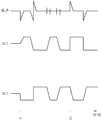
参照图5,图5为根据本发明一操作例所绘示的信号图。在本操作例中,波形SC1为对应输出缓冲器200输出的数据电压,波形SC2为对应输出缓冲器250输出的数据电压。在本操作例中,由于输出缓冲器200与输出缓冲器250分别用以输出彼此极性相反的数据电压,故波形SC1与波形SC2彼此大致相反。在本操作例,噪声Noise表示触控元件上量测到的噪声。Referring to FIG. 5 , FIG. 5 is a signal diagram according to an operation example of the present invention. In this operation example, the waveform SC1 corresponds to the data voltage output from the
在时间点t1时,触控元件量测到一负向噪声。此时,若使输出缓冲器200输出的数据电压的上升变化率增加,则可抵销或减缓此一负向噪声。另外,类似地,在时间点t2时,触控元件量测到一正向噪声。此时,若使输出缓冲器200输出的数据电压的上升变化率减低,则可抵销或减缓此一正向噪声。At time point t1, the touch element measures a negative noise. At this time, if the rising rate of change of the data voltage output from the
通过上述的操作,驱动电路120即可通过调整开关电路201、203的开关宽度,以使输出缓冲器200、250输出的数据电压的上升变化率与下降变化率彼此不同,以对触控元件量测到的噪声进行调整。Through the above-mentioned operations, the driving
应注意到,虽然在上述实施例中,是以对触控元件量测到的噪声进行调整为例进行说明,然而本案不以此为限。通过上述的操作,也可调整其它相关元件上的噪声。It should be noted that although in the above embodiments, the adjustment of the noise measured by the touch element is used as an example for description, but the present application is not limited to this. Through the above operations, the noise on other related components can also be adjusted.
图6为根据本发明另一实施例所绘示的驱动电路120的示意图。在本实施例中,开关电路202、204的开关宽度是可调整的。由此,驱动电路120即可通过调整开关电路202、204的开关宽度,以使输出缓冲器200、205输出的数据电压的上升变化率与下降变化率彼此不同,以对噪声进行调整。FIG. 6 is a schematic diagram of a
图7为根据本发明另一实施例所绘示的驱动电路120的示意图。在本实施例中,开关电路201-204的开关宽度是可调整的。由此,驱动电路120即可通过调整开关电路201-204的开关宽度,以使输出缓冲器200、205输出的数据电压的上升变化率与下降变化率彼此不同,以对噪声进行调整。FIG. 7 is a schematic diagram of a
图8为根据本发明另一实施例所绘示的驱动电路120的示意图。在本实施例中,驱动电路120包括输出缓冲器200a、输出开关OS1、输出缓冲器250a、输出开关OS2、及电流源IS1、IS2。在一实施例中,输出缓冲器200a的输出端电性连接于输出开关OS1,且输出缓冲器250a的输出端电性连接输出开关OS2。在一实施例中,输出缓冲器200a、250a彼此相邻设置。在一实施例中,电流源IS1电性连接于输出缓冲器200a,且电流源IS2电性连接于输出缓冲器250a。在一实施例中,输出缓冲器200a、250a用以输出数据电压(如分别用以输出数据电压D(1)、D(2))。在一实施例中,输出开关OS1、OS2用以相应于锁存信号(未示出)将数据电压提供至像素阵列101。在一实施例中,电流源IS1用以提供偏压电流I1至输出缓冲器200a,且电流源IS2用以提供偏压电流I2至输出缓冲器250a。FIG. 8 is a schematic diagram of a
在一实施例中,电流源IS1为可调电流源。在一实施例中,电流源IS1提供至输出缓冲器200a的偏压电流I1的电流量是可调整的,以调整输出缓冲器200a的转换率(slewrate)。在一实施例中,电流源IS1是根据调整信号ADS1调整偏压电流I1的电流量。另外,在一实施例中,电流源IS2为固定电流源,然本案不以此为限。In one embodiment, the current source IS1 is an adjustable current source. In one embodiment, the amount of bias current I1 provided by the current source IS1 to the
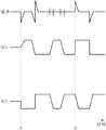
参照图9,图9为根据本发明另一操作例所绘示的信号图。在本操作例中,波形SC1为对应输出缓冲器200a输出的数据电压,波形SC2为对应输出缓冲器250a输出的数据电压。在本操作例中,由于输出缓冲器200a与输出缓冲器250a分别用以输出彼此极性相反的数据电压,故波形SC1与波形SC2彼此大致相反。在本操作例,噪声Noise表示触控元件上量测到的噪声。Referring to FIG. 9 , FIG. 9 is a signal diagram according to another operation example of the present invention. In this operation example, the waveform SC1 corresponds to the data voltage output from the
在时间点t1时,触控元件量测到一负向噪声。此时,若使偏压电流I1增加,以令输出缓冲器200a的转换率增加,则可抵销或减缓此一负向噪声。另外,类似地,在时间点t2时,触控元件量测到一正向噪声。此时,若使偏压电流I1减少,以令输出缓冲器200a的转换率减低,则可抵销或减缓此一正向噪声。At time point t1, the touch element measures a negative noise. At this time, if the bias current I1 is increased to increase the slew rate of the
通过上述的操作,驱动电路120即可通过调整偏压电流I1,以使输出缓冲器200a、250a的转换率彼此不同,以对触控元件量测到的噪声进行调整。Through the above operations, the driving
应注意到,虽然在上述实施例中,是以对触控元件量测到的噪声进行调整为例进行说明,然而本案不以此为限。通过上述的操作,也可调整其它相关元件上的噪声。It should be noted that although in the above embodiments, the adjustment of the noise measured by the touch element is used as an example for description, but the present application is not limited to this. Through the above operations, the noise on other related components can also be adjusted.
图10为根据本发明另一实施例所绘示的驱动电路120的示意图。在本实施例中,电流源IS2可根据调整信号ADS2调整偏压电流I2的电流量。由此,驱动电路120即可通过调整偏压电流I2,以使输出缓冲器200a、250a的转换率彼此不同,以对噪声进行调整。FIG. 10 is a schematic diagram of a
图11为根据本发明另一实施例所绘示的驱动电路120的示意图。在本实施例中,电流源IS1、IS2可分别根据调整信号ADS1、ADS2调整偏压电流I1、I2的电流量。由此,驱动电路120即可通过调整偏压电流I1、I2,以使输出缓冲器200a、250a的转换率彼此不同,以对噪声进行调整。FIG. 11 is a schematic diagram of a
虽然本发明已以实施例公开如上,然其并非用以限定本发明,任何本领域技术人员,在不脱离本发明的精神和范围内,可当作各种的更动与润饰,因此本发明的保护范围当视权利要求为准。Although the present invention has been disclosed as above with examples, it is not intended to limit the present invention. Any person skilled in the art can make various changes and modifications without departing from the spirit and scope of the present invention. Therefore, the present invention The scope of protection shall be subject to the claims.
Claims (10)
Applications Claiming Priority (2)
| Application Number | Priority Date | Filing Date | Title |
|---|---|---|---|
| TW108108305ATW202034301A (en) | 2019-03-12 | 2019-03-12 | Driver circuit for display panel |
| TW108108305 | 2019-03-12 |
Publications (1)
| Publication Number | Publication Date |
|---|---|
| CN111696465Atrue CN111696465A (en) | 2020-09-22 |
Family
ID=72476021
Family Applications (1)
| Application Number | Title | Priority Date | Filing Date |
|---|---|---|---|
| CN201910419654.0APendingCN111696465A (en) | 2019-03-12 | 2019-05-20 | Driving circuit of display panel |
Country Status (2)
| Country | Link |
|---|---|
| CN (1) | CN111696465A (en) |
| TW (1) | TW202034301A (en) |
Citations (6)
| Publication number | Priority date | Publication date | Assignee | Title |
|---|---|---|---|---|
| US20070080723A1 (en)* | 2005-10-06 | 2007-04-12 | Samsung Electro-Mechanics Co., Ltd. | Output buffer circuit |
| US20080278473A1 (en)* | 2007-05-11 | 2008-11-13 | Samsung Electronics Co., Ltd. | Source line driver and method for controlling slew rate according to temperature and display device including the source line driver |
| US20090256827A1 (en)* | 2008-04-15 | 2009-10-15 | Sony Corporation | Display device and output buffer circuit for driving the same |
| CN101714868A (en)* | 2008-09-30 | 2010-05-26 | 奇景光电股份有限公司 | Output buffer and source driver using the same |
| US20140292735A1 (en)* | 2013-03-29 | 2014-10-02 | Sony Corporation | Display device, cmos operational amplifier, and driving method of display device |
| CN108694902A (en)* | 2017-03-29 | 2018-10-23 | 美格纳半导体有限公司 | Source driver arrangement for display panel |
- 2019
- 2019-03-12TWTW108108305Apatent/TW202034301A/enunknown
- 2019-05-20CNCN201910419654.0Apatent/CN111696465A/enactivePending
Patent Citations (6)
| Publication number | Priority date | Publication date | Assignee | Title |
|---|---|---|---|---|
| US20070080723A1 (en)* | 2005-10-06 | 2007-04-12 | Samsung Electro-Mechanics Co., Ltd. | Output buffer circuit |
| US20080278473A1 (en)* | 2007-05-11 | 2008-11-13 | Samsung Electronics Co., Ltd. | Source line driver and method for controlling slew rate according to temperature and display device including the source line driver |
| US20090256827A1 (en)* | 2008-04-15 | 2009-10-15 | Sony Corporation | Display device and output buffer circuit for driving the same |
| CN101714868A (en)* | 2008-09-30 | 2010-05-26 | 奇景光电股份有限公司 | Output buffer and source driver using the same |
| US20140292735A1 (en)* | 2013-03-29 | 2014-10-02 | Sony Corporation | Display device, cmos operational amplifier, and driving method of display device |
| CN108694902A (en)* | 2017-03-29 | 2018-10-23 | 美格纳半导体有限公司 | Source driver arrangement for display panel |
Also Published As
| Publication number | Publication date |
|---|---|
| TW202034301A (en) | 2020-09-16 |
Similar Documents
| Publication | Publication Date | Title |
|---|---|---|
| US8928362B2 (en) | Semiconductor device and electronic apparatus using the same | |
| JP2021061624A (en) | Liquid crystal display device | |
| CN1161789C (en) | Semiconductor device | |
| US7623109B2 (en) | Display device | |
| US8847635B2 (en) | Self-calibration of output buffer driving strength | |
| CN101378252B (en) | Delay circuit, semiconductor control circuit, display device, and electronic device | |
| US20080042741A1 (en) | Light emitting device and current mirror thereof | |
| CN103383832B (en) | The driving method and electronic equipment of display device, display device | |
| US7750689B1 (en) | High voltage switch with reduced voltage stress at output stage | |
| CN109523946B (en) | Pixel circuit, display device, and pixel circuit driving method | |
| CN110070826B (en) | pixel circuit | |
| US11315490B2 (en) | Pixel circuit having a voltage amplification circuit and driving method thereof, display panel | |
| CN111696465A (en) | Driving circuit of display panel | |
| TWI694433B (en) | Pixel circuit | |
| US7365715B2 (en) | Electronic circuit, electronic device and personal computer | |
| CN108648685A (en) | Shift register cell and its driving method, gate driving circuit and display device | |
| JP2008283545A (en) | Signal level conversion circuit, and flat display device | |
| KR100432573B1 (en) | Semiconductor device having an output drive circuit capable of impedance adjustment | |
| JPWO2023026919A5 (en) | ||
| US7333099B2 (en) | Electronic circuit, display device, and electronic apparatus | |
| US12009821B2 (en) | Output driver and output buffer circuit including the same | |
| US7595662B2 (en) | Transmission/reception apparatus for differential signals | |
| CN110034754B (en) | An integrated circuit and its transmission circuit | |
| JP2000347635A (en) | Display drive device, display device, portable electronic device, and display drive method | |
| CN100429690C (en) | Current steering circuit for controlling gain error |
Legal Events
| Date | Code | Title | Description |
|---|---|---|---|
| PB01 | Publication | ||
| PB01 | Publication | ||
| SE01 | Entry into force of request for substantive examination | ||
| SE01 | Entry into force of request for substantive examination | ||
| WD01 | Invention patent application deemed withdrawn after publication | ||
| WD01 | Invention patent application deemed withdrawn after publication | Application publication date:20200922 |