CN111696444B - A display panel and its manufacturing method and display device - Google Patents
A display panel and its manufacturing method and display deviceDownload PDFInfo
- Publication number
- CN111696444B CN111696444BCN202010704341.2ACN202010704341ACN111696444BCN 111696444 BCN111696444 BCN 111696444BCN 202010704341 ACN202010704341 ACN 202010704341ACN 111696444 BCN111696444 BCN 111696444B
- Authority
- CN
- China
- Prior art keywords
- reflection
- display substrate
- transparent insulating
- display panel
- insulating layer
- Prior art date
- Legal status (The legal status is an assumption and is not a legal conclusion. Google has not performed a legal analysis and makes no representation as to the accuracy of the status listed.)
- Active
Links
Images


Classifications
- G—PHYSICS
- G09—EDUCATION; CRYPTOGRAPHY; DISPLAY; ADVERTISING; SEALS
- G09F—DISPLAYING; ADVERTISING; SIGNS; LABELS OR NAME-PLATES; SEALS
- G09F9/00—Indicating arrangements for variable information in which the information is built-up on a support by selection or combination of individual elements
- G09F9/30—Indicating arrangements for variable information in which the information is built-up on a support by selection or combination of individual elements in which the desired character or characters are formed by combining individual elements
- G09F9/301—Indicating arrangements for variable information in which the information is built-up on a support by selection or combination of individual elements in which the desired character or characters are formed by combining individual elements flexible foldable or roll-able electronic displays, e.g. thin LCD, OLED
- G—PHYSICS
- G06—COMPUTING OR CALCULATING; COUNTING
- G06F—ELECTRIC DIGITAL DATA PROCESSING
- G06F3/00—Input arrangements for transferring data to be processed into a form capable of being handled by the computer; Output arrangements for transferring data from processing unit to output unit, e.g. interface arrangements
- G06F3/01—Input arrangements or combined input and output arrangements for interaction between user and computer
- G06F3/03—Arrangements for converting the position or the displacement of a member into a coded form
- G06F3/041—Digitisers, e.g. for touch screens or touch pads, characterised by the transducing means
- G06F3/0412—Digitisers structurally integrated in a display
- G—PHYSICS
- G06—COMPUTING OR CALCULATING; COUNTING
- G06F—ELECTRIC DIGITAL DATA PROCESSING
- G06F3/00—Input arrangements for transferring data to be processed into a form capable of being handled by the computer; Output arrangements for transferring data from processing unit to output unit, e.g. interface arrangements
- G06F3/01—Input arrangements or combined input and output arrangements for interaction between user and computer
- G06F3/03—Arrangements for converting the position or the displacement of a member into a coded form
- G06F3/041—Digitisers, e.g. for touch screens or touch pads, characterised by the transducing means
- G06F3/044—Digitisers, e.g. for touch screens or touch pads, characterised by the transducing means by capacitive means
- G06F3/0443—Digitisers, e.g. for touch screens or touch pads, characterised by the transducing means by capacitive means using a single layer of sensing electrodes
- G—PHYSICS
- G06—COMPUTING OR CALCULATING; COUNTING
- G06F—ELECTRIC DIGITAL DATA PROCESSING
- G06F3/00—Input arrangements for transferring data to be processed into a form capable of being handled by the computer; Output arrangements for transferring data from processing unit to output unit, e.g. interface arrangements
- G06F3/01—Input arrangements or combined input and output arrangements for interaction between user and computer
- G06F3/03—Arrangements for converting the position or the displacement of a member into a coded form
- G06F3/041—Digitisers, e.g. for touch screens or touch pads, characterised by the transducing means
- G06F3/044—Digitisers, e.g. for touch screens or touch pads, characterised by the transducing means by capacitive means
- G06F3/0446—Digitisers, e.g. for touch screens or touch pads, characterised by the transducing means by capacitive means using a grid-like structure of electrodes in at least two directions, e.g. using row and column electrodes
- H—ELECTRICITY
- H10—SEMICONDUCTOR DEVICES; ELECTRIC SOLID-STATE DEVICES NOT OTHERWISE PROVIDED FOR
- H10K—ORGANIC ELECTRIC SOLID-STATE DEVICES
- H10K50/00—Organic light-emitting devices
- H10K50/80—Constructional details
- H10K50/86—Arrangements for improving contrast, e.g. preventing reflection of ambient light
- H10K50/865—Arrangements for improving contrast, e.g. preventing reflection of ambient light comprising light absorbing layers, e.g. light-blocking layers
- H—ELECTRICITY
- H10—SEMICONDUCTOR DEVICES; ELECTRIC SOLID-STATE DEVICES NOT OTHERWISE PROVIDED FOR
- H10K—ORGANIC ELECTRIC SOLID-STATE DEVICES
- H10K59/00—Integrated devices, or assemblies of multiple devices, comprising at least one organic light-emitting element covered by group H10K50/00
- H10K59/40—OLEDs integrated with touch screens
- H—ELECTRICITY
- H10—SEMICONDUCTOR DEVICES; ELECTRIC SOLID-STATE DEVICES NOT OTHERWISE PROVIDED FOR
- H10K—ORGANIC ELECTRIC SOLID-STATE DEVICES
- H10K59/00—Integrated devices, or assemblies of multiple devices, comprising at least one organic light-emitting element covered by group H10K50/00
- H10K59/80—Constructional details
- H10K59/8791—Arrangements for improving contrast, e.g. preventing reflection of ambient light
- H10K59/8792—Arrangements for improving contrast, e.g. preventing reflection of ambient light comprising light absorbing layers, e.g. black layers
- H—ELECTRICITY
- H10—SEMICONDUCTOR DEVICES; ELECTRIC SOLID-STATE DEVICES NOT OTHERWISE PROVIDED FOR
- H10K—ORGANIC ELECTRIC SOLID-STATE DEVICES
- H10K71/00—Manufacture or treatment specially adapted for the organic devices covered by this subclass
- G—PHYSICS
- G06—COMPUTING OR CALCULATING; COUNTING
- G06F—ELECTRIC DIGITAL DATA PROCESSING
- G06F2203/00—Indexing scheme relating to G06F3/00 - G06F3/048
- G06F2203/041—Indexing scheme relating to G06F3/041 - G06F3/045
- G06F2203/04103—Manufacturing, i.e. details related to manufacturing processes specially suited for touch sensitive devices
- G—PHYSICS
- G06—COMPUTING OR CALCULATING; COUNTING
- G06F—ELECTRIC DIGITAL DATA PROCESSING
- G06F2203/00—Indexing scheme relating to G06F3/00 - G06F3/048
- G06F2203/041—Indexing scheme relating to G06F3/041 - G06F3/045
- G06F2203/04111—Cross over in capacitive digitiser, i.e. details of structures for connecting electrodes of the sensing pattern where the connections cross each other, e.g. bridge structures comprising an insulating layer, or vias through substrate
- H—ELECTRICITY
- H10—SEMICONDUCTOR DEVICES; ELECTRIC SOLID-STATE DEVICES NOT OTHERWISE PROVIDED FOR
- H10K—ORGANIC ELECTRIC SOLID-STATE DEVICES
- H10K2102/00—Constructional details relating to the organic devices covered by this subclass
- H10K2102/301—Details of OLEDs
- H10K2102/311—Flexible OLED
- H—ELECTRICITY
- H10—SEMICONDUCTOR DEVICES; ELECTRIC SOLID-STATE DEVICES NOT OTHERWISE PROVIDED FOR
- H10K—ORGANIC ELECTRIC SOLID-STATE DEVICES
- H10K59/00—Integrated devices, or assemblies of multiple devices, comprising at least one organic light-emitting element covered by group H10K50/00
- H10K59/30—Devices specially adapted for multicolour light emission
- H10K59/35—Devices specially adapted for multicolour light emission comprising red-green-blue [RGB] subpixels
Landscapes
- Engineering & Computer Science (AREA)
- Theoretical Computer Science (AREA)
- General Engineering & Computer Science (AREA)
- Physics & Mathematics (AREA)
- General Physics & Mathematics (AREA)
- Human Computer Interaction (AREA)
- Manufacturing & Machinery (AREA)
- Optics & Photonics (AREA)
- Electroluminescent Light Sources (AREA)
Abstract
Description
Translated fromChinese技术领域technical field
本发明属于显示技术领域,具体涉及一种显示面板及其制备方法和显示装置。The invention belongs to the field of display technology, and in particular relates to a display panel, a preparation method thereof, and a display device.
背景技术Background technique
当前OLED(OrganicLight-Emitting Diode,有机电激光显示)显示技术中通常需要圆偏光片,触控层,并通过胶材贴合组成显示模组,圆偏光片起到降低OLED表面反射并提高对比度的功能,触控层起到触控作用。由于圆偏光片厚度较大,导致整体模组厚度偏大,影响柔性模组的反复折叠能力。In the current OLED (OrganicLight-Emitting Diode, organic electro-optical laser display) display technology, a circular polarizer and a touch layer are usually required, and a display module is formed by laminating with adhesive materials. The circular polarizer can reduce the surface reflection of the OLED and improve the contrast ratio. function, the touch layer plays the role of touch. Due to the large thickness of the circular polarizer, the thickness of the overall module is too large, which affects the repeated folding ability of the flexible module.
发明内容SUMMARY OF THE INVENTION
本发明针对OLED显示模组中同时集成圆偏光片降反射和触控层触控时导致的整体模组厚度偏大,影响柔性模组的折叠能力的问题,提供一种显示面板及其制备方法和显示装置。该显示面板,在实现防反射的同时,还能实现触控功能;同时能降低显示面板的整体厚度,从而具有良好的反复折叠能力;同时,能使显示面板的防反射功能与触控功能良好兼容。The present invention provides a display panel and a preparation method thereof, aiming at the problem that the thickness of the overall module is too large when the circular polarizer anti-reflection and the touch control layer are simultaneously integrated in the OLED display module, which affects the folding ability of the flexible module. and display device. The display panel can realize anti-reflection and touch function at the same time; at the same time, the overall thickness of the display panel can be reduced, so that it has good repeated folding ability; at the same time, the anti-reflection function and touch function of the display panel can be improved. compatible.
本发明提供一种显示面板,包括显示基板,设置于所述显示基板一侧的触控电极和防反射结构,所述显示基板包括多个间隔排布的子像素,所述触控电极在所述显示基板上的正投影位于相邻所述子像素之间的间隔区;所述防反射结构包括多个,各所述防反射结构在所述显示基板上的正投影对应覆盖各所述子像素,且所述防反射结构在所述显示基板上的正投影与所述触控电极在所述显示基板上的正投影不交叠。The present invention provides a display panel, which includes a display substrate, a touch electrode and an anti-reflection structure disposed on one side of the display substrate, the display substrate includes a plurality of sub-pixels arranged at intervals, and the touch electrode is located on the side of the display substrate. The orthographic projection on the display substrate is located in the space between adjacent sub-pixels; the anti-reflection structure includes a plurality of, and the orthographic projection of each anti-reflection structure on the display substrate corresponds to covering each of the sub-pixels pixel, and the orthographic projection of the anti-reflection structure on the display substrate does not overlap with the orthographic projection of the touch electrodes on the display substrate.
可选地,所述防反射结构包括至少一个防反射金属层和至少两个透明绝缘层,所述透明绝缘层和所述防反射金属层依次交错叠置,且所述防反射金属层夹设于相邻的两所述透明绝缘层之间;Optionally, the anti-reflection structure includes at least one anti-reflection metal layer and at least two transparent insulating layers, the transparent insulating layers and the anti-reflection metal layers are alternately stacked in sequence, and the anti-reflection metal layers are sandwiched. between two adjacent transparent insulating layers;
所述防反射结构位于所述触控电极的背离所述显示基板的一侧,所述防反射结构包括依次远离所述触控电极排布的第一透明绝缘层、防反射金属层和第二透明绝缘层。The anti-reflection structure is located on the side of the touch electrode away from the display substrate, and the anti-reflection structure includes a first transparent insulating layer, an anti-reflection metal layer and a second transparent insulating layer arranged away from the touch electrode in sequence. Transparent insulating layer.
可选地,所述第一透明绝缘层和所述第二透明绝缘层还延伸至相邻所述子像素之间的间隔区。Optionally, the first transparent insulating layer and the second transparent insulating layer further extend to spacers between adjacent sub-pixels.
可选地,在所述显示基板上,正投影相邻的所述防反射金属层与所述触控电极之间的正投影间距大于或等于0.1μm。Optionally, on the display substrate, the orthographic spacing between the adjacent anti-reflection metal layers and the touch electrodes in orthographic projections is greater than or equal to 0.1 μm.
可选地,所述触控电极呈网格状,多个所述防反射结构中的所述防反射金属层不连续分布,各所述防反射结构中的所述防反射金属层呈块状。Optionally, the touch electrodes are in a grid shape, the anti-reflection metal layers in the plurality of anti-reflection structures are discontinuously distributed, and the anti-reflection metal layers in each of the anti-reflection structures are in a block shape .
可选地,所述防反射金属层采用Ti、Mo、Cu、Al、Ag中的任意一种材料;所述防反射金属层的厚度范围为10~1000埃。Optionally, the anti-reflection metal layer is made of any one of Ti, Mo, Cu, Al, and Ag; the thickness of the anti-reflection metal layer ranges from 10 to 1000 angstroms.
可选地,所述第一透明绝缘层的厚度范围为50-50000埃,所述第二透明绝缘层的厚度范围为50-50000埃;Optionally, the thickness of the first transparent insulating layer is in the range of 50-50,000 angstroms, and the thickness of the second transparent insulating layer is in the range of 50-50,000 angstroms;
所述第一透明绝缘层的折射率范围为1.4~2.0,所述第二透明绝缘层的折射率范围为1.4~2.0;The refractive index of the first transparent insulating layer ranges from 1.4 to 2.0, and the refractive index of the second transparent insulating layer ranges from 1.4 to 2.0;
所述第一透明绝缘层采用氧化硅、氮化硅或有机树脂材料;所述第二透明绝缘层采用氧化硅、氮化硅或有机树脂材料。The first transparent insulating layer is made of silicon oxide, silicon nitride or organic resin material; the second transparent insulating layer is made of silicon oxide, silicon nitride or organic resin material.
可选地,还包括黑矩阵,所述黑矩阵设置于所述第二透明绝缘层的背离所述显示基板的一侧;Optionally, it also includes a black matrix, and the black matrix is disposed on a side of the second transparent insulating layer away from the display substrate;
所述黑矩阵在所述显示基板上的正投影覆盖相邻所述子像素之间的间隔区,且所述黑矩阵在所述显示基板上的正投影覆盖相邻所述防反射结构中所述防反射金属层在所述显示基板上的正投影的边缘。The orthographic projection of the black matrix on the display substrate covers the space between adjacent sub-pixels, and the orthographic projection of the black matrix on the display substrate covers the adjacent anti-reflection structures. The edge of the orthographic projection of the anti-reflection metal layer on the display substrate.
可选地,所述黑矩阵在所述显示基板上的正投影边缘线与所述防反射金属层在所述显示基板上的正投影边缘线之间的最短间距大于或等于0.1μm。Optionally, the shortest distance between the orthographic projection edge line of the black matrix on the display substrate and the orthographic projection edge line of the anti-reflection metal layer on the display substrate is greater than or equal to 0.1 μm.
可选地,所述触控电极包括驱动电极、感应电极和桥部;所述驱动电极包括多个,各所述驱动电极沿第一方向延伸并沿第二方向依次排布;所述感应电极包括多个,各所述感应电极沿所述第二方向延伸并沿所述第一方向依次排布;Optionally, the touch electrodes include drive electrodes, sensing electrodes, and bridges; the drive electrodes include a plurality of drive electrodes, each of which extends along a first direction and is sequentially arranged along a second direction; the sensing electrodes including a plurality of inductive electrodes, each of which extends along the second direction and is sequentially arranged along the first direction;
所述驱动电极和所述感应电极同层设置且相互绝缘,所述桥部设置于所述驱动电极和所述感应电极的靠近所述显示基板的一侧,且所述桥部与所述驱动电极和所述感应电极之间设置有绝缘层。The driving electrodes and the sensing electrodes are arranged in the same layer and insulated from each other, the bridge portion is arranged on the side of the driving electrodes and the sensing electrodes close to the display substrate, and the bridge portion is connected to the driving electrode and the driving electrode. An insulating layer is arranged between the electrodes and the sensing electrodes.
可选地,所述驱动电极、所述感应电极和所述桥部在所述显示基板上的正投影分别落入相邻所述子像素之间的间隔区。Optionally, the orthographic projections of the driving electrodes, the sensing electrodes and the bridges on the display substrate respectively fall into spaced regions between adjacent sub-pixels.
本发明还提供一种显示装置,包括上述显示面板。The present invention also provides a display device including the above-mentioned display panel.
本发明还提供一种显示面板的制备方法,包括制备显示基板,在所述显示基板的一侧制备触控电极和防反射结构;制备所述显示基板包括制备多个间隔排布的子像素,所述触控电极在所述显示基板上的正投影位于相邻所述子像素之间的间隔区;所述防反射结构包括多个,各所述防反射结构在所述显示基板上的正投影对应覆盖各所述子像素,且所述防反射结构在所述显示基板上的正投影与所述触控电极在所述显示基板上的正投影不交叠。The present invention also provides a method for preparing a display panel, including preparing a display substrate, preparing a touch electrode and an anti-reflection structure on one side of the display substrate; preparing the display substrate includes preparing a plurality of sub-pixels arranged at intervals, The orthographic projections of the touch electrodes on the display substrate are located in the spaced regions between the adjacent sub-pixels; the anti-reflection structures include a plurality of anti-reflection structures, and each anti-reflection structure has an orthographic projection on the display substrate. The projection covers each of the sub-pixels correspondingly, and the orthographic projection of the anti-reflection structure on the display substrate does not overlap with the orthographic projection of the touch electrodes on the display substrate.
本发明的有益效果:本发明所提供的显示面板,通过在显示基板的一侧设置触控电极和防反射结构,在实现该显示面板防反射的同时,还能实现显示面板的触控功能;通过采用厚度较薄的防反射结构,能够替代目前厚度较大的圆偏光片,从而降低显示面板的整体厚度,进而使具有柔性性能的显示面板具有良好的反复折叠能力;同时,通过使防反射结构设置为多个,且防反射结构在显示基板上的正投影与触控电极在显示基板上的正投影不交叠,能够降低或消除防反射结构中防反射金属层的导电效应,减少防反射金属层对触控电极触控信号的干扰,从而使显示面板的防反射功能与触控功能能够良好兼容。Beneficial effects of the present invention: the display panel provided by the present invention can realize the touch function of the display panel while realizing the anti-reflection of the display panel by arranging the touch electrodes and the anti-reflection structure on one side of the display substrate; By adopting an anti-reflection structure with a thinner thickness, the current circular polarizer with a larger thickness can be replaced, thereby reducing the overall thickness of the display panel, so that the display panel with flexible performance has good repeated folding ability; at the same time, by making the anti-reflection structure The structure is arranged in multiples, and the orthographic projection of the anti-reflection structure on the display substrate does not overlap with the orthographic projection of the touch electrodes on the display substrate, which can reduce or eliminate the conductive effect of the anti-reflection metal layer in the anti-reflection structure, and reduce the anti-reflection structure. The reflection metal layer interferes with the touch signal of the touch electrode, so that the anti-reflection function of the display panel can be well compatible with the touch function.
本发明所提供的显示装置,通过采用上述显示面板,能够实现该显示装置的防反射功能与触控功能良好兼容,同时还能降低显示装置的整体厚度,从而使该显示装置具有良好的耐弯折能力,便于实现柔性显示。In the display device provided by the present invention, by using the above-mentioned display panel, the anti-reflection function and the touch function of the display device can be well compatible, and at the same time, the overall thickness of the display device can be reduced, so that the display device has good bending resistance. Folding ability, easy to achieve flexible display.
附图说明Description of drawings
图1为本发明实施例中一种显示面板的结构剖视示意图;FIG. 1 is a schematic cross-sectional view of the structure of a display panel according to an embodiment of the present invention;
图2为本发明实施例中一种显示面板的结构俯视示意图;2 is a schematic top view of the structure of a display panel according to an embodiment of the present invention;
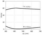
图3为由图1显示面板中的第一透明绝缘层、防反射金属层、第二透明绝缘层构成的吸光结构的透光率曲线和对光线的反射率曲线示意图;3 is a schematic diagram of a light transmittance curve and a light reflectance curve of a light absorption structure composed of a first transparent insulating layer, an anti-reflection metal layer, and a second transparent insulating layer in the display panel of FIG. 1;
图4为本发明实施例显示面板中触控电极的宏观分布示意图;4 is a schematic diagram of a macroscopic distribution of touch electrodes in a display panel according to an embodiment of the present invention;
图5为本发明实施例显示面板中触控电极的微观分布示意图。FIG. 5 is a schematic diagram of a microscopic distribution of touch electrodes in a display panel according to an embodiment of the present invention.
其中附图标记为:The reference numerals are:
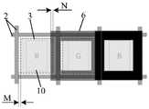
1、显示基板;10、子像素;11、背板;12、封装层;2、触控电极;21、驱动电极;22、感应电极;220、子部;23、桥部;3、防反射金属层;4、第一透明绝缘层;5、第二透明绝缘层;6、黑矩阵;7、第三透明绝缘层;8、防反射结构。1. Display substrate; 10. Sub-pixels; 11. Backplane; 12. Encapsulation layer; 2. Touch electrodes; 21. Drive electrodes; 22. Induction electrodes; Metal layer; 4. First transparent insulating layer; 5. Second transparent insulating layer; 6. Black matrix; 7. Third transparent insulating layer; 8. Anti-reflection structure.
具体实施方式Detailed ways
为使本领域技术人员更好地理解本发明的技术方案,下面结合附图和具体实施方式对本发明一种显示面板及其制备方法和显示装置作进一步详细描述。In order to enable those skilled in the art to better understand the technical solutions of the present invention, a display panel, a manufacturing method thereof, and a display device of the present invention are further described in detail below with reference to the accompanying drawings and specific embodiments.
基于目前存在的OLED显示模组中同时集成圆偏光片降反射和触控层触控时导致的整体模组厚度偏大,影响柔性模组的折叠能力的问题,本发明实施例提供一种显示面板,如图1所示,包括显示基板1,设置于显示基板1一侧的触控电极2和防反射结构8,显示基板1包括多个间隔排布的子像素10,触控电极2在显示基板1上的正投影位于相邻子像素10之间的间隔区;防反射结构8包括多个,各防反射结构8在显示基板1上的正投影对应覆盖各子像素10,且防反射结构8在显示基板1上的正投影与触控电极2在显示基板1上的正投影不交叠。Based on the problem that the thickness of the overall module is too large when the circular polarizer anti-reflection and touch layer touch are simultaneously integrated in the existing OLED display module, which affects the folding ability of the flexible module, the embodiment of the present invention provides a display The panel, as shown in FIG. 1 , includes a display substrate 1 , a
其中,防反射结构8与触控电极2不同层设置。子像素10包括呈阵列排布的红色子像素、绿色子像素和蓝色子像素,由至少一个红色子像素、至少一个绿色子像素和至少一个蓝色子像素构成一个像素,例如可以是两个绿色子像素、一个红色子像素和一个蓝色子像素构成一个像素。可选地,子像素10为OLED(有机电致发光元件),子像素10包括依次叠置的阳极、发光功能层和阴极。显示基板1包括背板11和设置在背板11上的子像素10(即发光元件),子像素10的背离背板11的一侧设置有封装层12,触控电极2和防反射结构8设置于封装层12的背离背板11的一侧。背板11上设置有像素驱动电路(图中未示出),用于驱动子像素10发光。Wherein, the anti-reflection structure 8 and the
可选地,防反射结构8包括至少一个防反射金属层3和至少两个透明绝缘层,透明绝缘层和防反射金属层3依次交错叠置,且防反射金属层3夹设于相邻的两透明绝缘层之间;透明绝缘层还延伸至相邻子像素10之间的间隔区。Optionally, the anti-reflection structure 8 includes at least one anti-reflection metal layer 3 and at least two transparent insulating layers, the transparent insulating layer and the anti-reflection metal layer 3 are alternately stacked in sequence, and the anti-reflection metal layer 3 is sandwiched between adjacent ones. between the two transparent insulating layers; the transparent insulating layer also extends to the space between adjacent sub-pixels 10 .
通过在显示基板1的一侧设置触控电极2和防反射结构8,在实现该显示面板防反射的同时,还能实现显示面板的触控功能;通过采用厚度较薄的防反射结构8,能够替代目前厚度较大的圆偏光片,从而降低显示面板的整体厚度,进而使具有柔性性能的显示面板具有良好的反复折叠能力;同时,通过使防反射结构8设置为多个,且防反射结构8在显示基板1上的正投影与触控电极2在显示基板1上的正投影不交叠,能够降低或消除防反射结构8中防反射金属层3的导电效应,减少防反射金属层3对触控电极2触控信号的干扰,从而使显示面板的防反射功能与触控功能能够良好兼容。By arranging the
可选地,如图2所示,在显示基板上,正投影相邻的防反射金属层3与触控电极2之间的正投影间距M大于或等于0.1μm。该间距范围,能够更好地降低或消除防反射金属层3的导电效应,减少防反射金属层3对触控电极2触控信号的干扰,从而使显示面板的防反射功能与触控功能能够良好兼容。Optionally, as shown in FIG. 2 , on the display substrate, the orthographic projection distance M between the orthographically adjacent anti-reflection metal layers 3 and the
可选地,触控电极2呈网格状,多个防反射结构8中的防反射金属层3不连续分布,各防反射结构8中的防反射金属层3呈块状。如触控电极2采用Ti/Al/Ti叠层,触控电极2呈网格状,且触控电极2位于子像素10之间的间隔区,既能实现触控电极2在显示面板上的整面触控,又不会影响显示面板的正常显示透光。防反射金属层3采用块状,能够对外界照射至其上的光线进行很好的耗散,防止外界环境光照射到阳极后反射对显示对比度的影响。Optionally, the
可选地,防反射结构8位于触控电极2的背离显示基板1的一侧,防反射结构8包括依次远离触控电极2排布的第一透明绝缘层4、防反射金属层3和第二透明绝缘层5。如此设置,防反射金属层3与第一透明绝缘层4和第二透明绝缘层5共同构成的防反射结构8,能够更好地对外界环境光进行耗散,且通过第一透明绝缘层4的设置,能够很好地减少或防止防反射金属层3对触控电极2触控信号的干扰,从而使显示面板的防反射功能与触控功能能够良好兼容。Optionally, the anti-reflection structure 8 is located on the side of the
可选地,防反射金属层3采用Ti、Mo、Cu、Al、Ag中的任意一种材料。防反射金属层3的厚度范围为10~1000埃。这些材料的防反射金属层3在具有一定厚度的情况下,搭配其上下表面的第一透明绝缘层4和第二透明绝缘层5,可实现本体低反射,且具备透过的特性,外界光在防反射结构8内耗散,降低反射光,同时OLED的光可以透过防反射金属层3,从而实现显示面板的正常显示。Optionally, the anti-reflection metal layer 3 is made of any one of Ti, Mo, Cu, Al, and Ag. The thickness of the anti-reflection metal layer 3 ranges from 10 to 1000 angstroms. When the anti-reflection metal layer 3 of these materials has a certain thickness, with the first transparent insulating
可选地,第一透明绝缘层4的厚度范围为50-50000埃,第二透明绝缘层5的厚度范围为50-50000埃。第一透明绝缘层4的折射率范围为1.4~2.0,第二透明绝缘层5的折射率范围为1.4~2.0。第一透明绝缘层4采用氧化硅、氮化硅或有机树脂材料;第二透明绝缘层5采用氧化硅、氮化硅或有机树脂材料。Optionally, the thickness of the first transparent insulating
其中,防反射金属层3与相邻的第一透明绝缘层4和第二透明绝缘层5共同构成了吸光结构,如图3所示,该吸光结构的透过率约为20-70%可调,优选35-60%,黑矩阵BM近似为黑体,常规OLED显示面板本身反射率约46%,集成该吸光结构后,其反射率降到5%,且同时具备触控功能。例如:使用第一透明绝缘层4/防反射金属层3/第二透明绝缘层5的材质为氧化硅/钛/氧化硅,厚度为80nm/5nm/80nm的三层结构时,该吸光结构本身透过率为58%,反射率为3%,与触控电极2和黑矩阵6搭配设置后,使OLED显示面板表面反射率从46%降低至8%,通过调整防反射金属层3的厚度,能使OLED显示面板的透过率调整至45-50%,反射率降到5%,满足OLED显示面板的显示以及防反射要求,同时其触控电极2可以正常触控,实现该显示面板的触控功能。The anti-reflection metal layer 3 and the adjacent first transparent insulating
需要说明的是,显示基板1的一侧可以设置缓冲层,触控电极2设置于封装层背离显示基板一测。由于显示基板1中用于对子像素10进行封装的封装层12通常采用有机膜层和无机膜层的叠置膜层,为增加触控电极的粘附性,可在封装层12上设置缓冲层。It should be noted that a buffer layer may be provided on one side of the display substrate 1, and the
可选地,显示面板还包括黑矩阵6,黑矩阵6设置于第二透明绝缘层5的背离显示基板1的一侧;黑矩阵6在显示基板1上的正投影覆盖相邻子像素10之间的间隔区,且黑矩阵6在显示基板1上的正投影覆盖相邻防反射结构8中防反射金属层3在显示基板1上的正投影的边缘。黑矩阵6的材料为显示行业常用黑色强吸收材料,黑矩阵6能对防反射金属层3与触控电极2之间的间隙进行降反射,从而实现防反射金属层3与触控电极2的集成一体化,减小了显示面板的总体厚度,整合了触控功能和防反射功能,提升了显示面板的耐弯折能力。Optionally, the display panel further includes a black matrix 6, and the black matrix 6 is arranged on the side of the second transparent insulating
可选地,子像素10包括呈阵列排布的红色子像素、绿色子像素和蓝色子像素,由红色子像素、绿色子像素和蓝色子像素构成一个像素。可选地,子像素10为OLED(有机电致发光元件),黑矩阵6的设置还能防止不同颜色的子像素10之间发生颜色串扰。Optionally, the sub-pixels 10 include red sub-pixels, green sub-pixels and blue sub-pixels arranged in an array, and one pixel is constituted by the red sub-pixels, the green sub-pixels and the blue sub-pixels. Optionally, the sub-pixels 10 are OLEDs (organic electroluminescent elements), and the arrangement of the black matrix 6 can also prevent color crosstalk between
可选地,如图2所示,黑矩阵6在显示基板1上的正投影边缘线与防反射金属层3在显示基板1上的正投影边缘线之间的最短间距N大于或等于0.1μm。即黑矩阵6在显示基板1上的正投影覆盖相邻防反射金属层3在显示基板1上的正投影的边缘宽度为0.1μm以上。由于黑矩阵6近似为不反射的黑体,如此设置,能使黑矩阵6对防反射金属层3与触控电极2之间的间隙进行降反射,避免防反射金属层3与触控电极2之间的间隙处表面反射率太高,从而实现防反射金属层3与触控电极2的集成一体化,减小了显示面板的总体厚度,整合了触控功能和防反射功能,提升了显示面板的耐弯折能力。Optionally, as shown in FIG. 2 , the shortest distance N between the orthographic projection edge line of the black matrix 6 on the display substrate 1 and the orthographic projection edge line of the anti-reflection metal layer 3 on the display substrate 1 is greater than or equal to 0.1 μm . That is, the edge width of the orthographic projection of the black matrix 6 on the display substrate 1 covering the orthographic projection of the adjacent anti-reflection metal layer 3 on the display substrate 1 is 0.1 μm or more. Since the black matrix 6 is approximately a non-reflective black body, the setting in this way can reduce the reflection of the black matrix 6 on the gap between the anti-reflection metal layer 3 and the
可选地,如图1所示,显示面板还包括第三透明绝缘层7,第三透明绝缘层7设置于黑矩阵6的背离显示基板1的一侧。第三透明绝缘层7采用有机树脂材料、氧化硅或氮化硅材料。第三透明绝缘层7能对黑矩阵6以及整个显示基板1形成保护。Optionally, as shown in FIG. 1 , the display panel further includes a third transparent insulating layer 7 , and the third transparent insulating layer 7 is disposed on a side of the black matrix 6 away from the display substrate 1 . The third transparent insulating layer 7 is made of organic resin material, silicon oxide or silicon nitride material. The third transparent insulating layer 7 can protect the black matrix 6 and the entire display substrate 1 .
可选地,如图4和图5所示,触控电极2包括驱动电极21、感应电极22和桥部23;驱动电极21和感应电极22同层设置,桥部23设置于驱动电极21和感应电极22的靠近显示基板1的一侧,且桥部23与驱动电极21和感应电极22之间设置有绝缘层;驱动电极21包括多个,各驱动电极21沿第一方向X延伸并沿第二方向Y依次排布;感应电极22包括多个子部220,桥部23通过开设在绝缘层中的过孔将子部220连接为一体,感应电极22包括多个,各感应电极22沿第二方向Y延伸并沿第一方向X依次排布;驱动电极21与感应电极22相互绝缘;驱动电极21、感应电极22和桥部23在显示基板上的正投影分别落入相邻子像素之间的间隔区。驱动电极21与感应电极22能够实现互电容触控。Optionally, as shown in FIG. 4 and FIG. 5 , the
可选地,驱动电极21与感应电极22同层设置,桥部23与感应电极22不同层,且桥部23与感应电极22之间设置有绝缘层。当然,驱动电极21和感应电极22也可以不同层设置,即驱动电极21和感应电极22分别设置在不同的层上。Optionally, the driving
需要说明的是,驱动电极21和感应电极22也可以是能实现互电容触控的其他的排布方式,不局限于上述触控电极2排布方式。It should be noted that the driving
另外需要说明的是,能实现互电容触控的触控电极2的结构设置不局限于上述设置,其他的结构设置方式也完全可以,只要确保触控电极2在显示基板1上的正投影位于相邻子像素10之间的间隔区即可。In addition, it should be noted that the structural arrangement of the
另外需要说明的是,触控电极也可以是自电容式触控电极,自电容式触控电极既做驱动电极又做感测电极,单层多点式自容触控电极,触控电极引线与感测电极同层设置;多层式自容触控设计,触控电极引线与感测电极位于不同层,两层金属由绝缘层隔开,通过过孔设计使对应电极引线及感测电极进行导通,自电容式触控电极的排布为常规自电容触控电极的排布,这里不再赘述。In addition, it should be noted that the touch electrodes can also be self-capacitance touch electrodes, and the self-capacitance touch electrodes serve as both driving electrodes and sensing electrodes, single-layer multi-point self-capacitance touch electrodes, and touch electrode leads Set on the same layer as the sensing electrodes; multi-layer self-capacitive touch design, the touch electrode leads and the sensing electrodes are located on different layers, and the two layers of metal are separated by an insulating layer, and the corresponding electrode leads and the sensing electrodes are designed through the via hole. Conducting conduction, the arrangement of the self-capacitance touch electrodes is the arrangement of the conventional self-capacitance touch electrodes, which will not be repeated here.
基于显示面板的上述结构,本实施例还提供一种该显示面板的制备方法,包括制备显示基板,在显示基板的一侧制备触控电极和防反射结构;制备显示基板包括制备多个间隔排布的子像素,触控电极在显示基板上的正投影位于相邻子像素之间的间隔区;防反射结构包括多个,各防反射结构在显示基板上的正投影对应覆盖各子像素,且防反射结构在显示基板上的正投影与触控电极在显示基板上的正投影不交叠。Based on the above structure of the display panel, this embodiment also provides a method for manufacturing the display panel, which includes preparing a display substrate, preparing touch electrodes and an anti-reflection structure on one side of the display substrate; preparing the display substrate includes preparing a plurality of spacer rows The sub-pixels of the cloth, the orthographic projections of the touch electrodes on the display substrate are located in the spaced regions between adjacent sub-pixels; the anti-reflection structures include a plurality of anti-reflection structures, and the orthographic projections of the anti-reflection structures on the display substrate correspond to cover each sub-pixel, And the orthographic projection of the anti-reflection structure on the display substrate does not overlap with the orthographic projection of the touch electrodes on the display substrate.
本实施例中,显示面板的具体制备过程为:In this embodiment, the specific preparation process of the display panel is as follows:
步骤S01:在经过对子像素封装的显示基板表面制备缓冲层;Step S01: preparing a buffer layer on the surface of the display substrate encapsulated by the sub-pixels;
步骤S02:缓冲层表面沉积金属膜层并刻蚀形成桥部,金属膜层可以为Ti/Al/Ti叠层;Step S02: depositing a metal film layer on the surface of the buffer layer and etching to form a bridge portion, the metal film layer may be a Ti/Al/Ti stack;
步骤S03:使用氧化硅、氮化硅或者有机树脂材料图形化形成触控电极桥部与感应电极之间的绝缘跨桥及其中过孔;Step S03: using silicon oxide, silicon nitride or organic resin material to pattern an insulating bridge and a via hole between the touch electrode bridge and the sensing electrode;
步骤S04:沉积金属膜层并刻蚀形成感应电极和驱动电极,金属膜层可以为Ti/Al/Ti叠层;其中,桥部通过绝缘跨桥中的过孔连接感应电极;Step S04: depositing a metal film layer and etching to form a sensing electrode and a driving electrode, the metal film layer may be a Ti/Al/Ti stack; wherein, the bridge portion is connected to the sensing electrode through a via hole in the insulating bridge;
步骤S05:涂布第一透明绝缘层膜并固化;Step S05: coating and curing the first transparent insulating layer;
步骤S06:沉积防反射金属层膜,并图形化;沉积方法可以使用金属掩膜板真空蒸镀直接形成相互间隔且彼此独立的防反射金属层图形,也可以先使用物理气相沉积形成防反射金属层膜,然后曝光刻蚀形成相互间隔且彼此独立的防反射金属层图形;Step S06 : depositing an anti-reflection metal layer film and patterning; the deposition method can use a metal mask vacuum evaporation to directly form an anti-reflection metal layer pattern that is spaced apart and independent of each other, or can first use physical vapor deposition to form an anti-reflection metal layer layer film, and then exposure and etching to form anti-reflection metal layer patterns that are spaced apart and independent of each other;
步骤S07:沉积第二透明绝缘层;优选为氧化硅,厚度800A;Step S07: depositing a second transparent insulating layer; preferably silicon oxide, with a thickness of 800A;
步骤S08:涂布黑矩阵膜并曝光图形化;Step S08: coating the black matrix film and exposing and patterning;
步骤S09:涂布第三透明绝缘层并固化,完成显示面板的制备。Step S09 : coating and curing a third transparent insulating layer to complete the preparation of the display panel.
本实施例中所提供的显示面板,通过在显示基板的一侧设置触控电极和防反射结构,在实现该显示面板防反射的同时,还能实现显示面板的触控功能;通过采用厚度较薄的防反射结构,能够替代目前厚度较大的圆偏光片,从而降低显示面板的整体厚度,进而使具有柔性性能的显示面板具有良好的反复折叠能力;同时,通过使防反射结构设置为多个,且防反射结构在显示基板上的正投影与触控电极在显示基板上的正投影不交叠,能够降低或消除防反射结构中防反射金属层的导电效应,减少防反射金属层对触控电极触控信号的干扰,从而使显示面板的防反射功能与触控功能能够良好兼容。In the display panel provided in this embodiment, by arranging the touch electrodes and the anti-reflection structure on one side of the display substrate, the touch function of the display panel can be realized while the anti-reflection of the display panel is realized; The thin anti-reflection structure can replace the current thicker circular polarizer, thereby reducing the overall thickness of the display panel, so that the display panel with flexible performance has good repeated folding ability; at the same time, by setting the anti-reflection structure to multiple and the orthographic projection of the anti-reflection structure on the display substrate does not overlap with the orthographic projection of the touch electrodes on the display substrate, which can reduce or eliminate the conductive effect of the anti-reflection metal layer in the anti-reflection structure and reduce the impact of the anti-reflection metal layer on the The interference of the touch signal of the touch electrode, so that the anti-reflection function of the display panel and the touch function can be well compatible.
本公开实施例还提供一种显示装置,包括上述实施例中的显示面板。Embodiments of the present disclosure also provide a display device, including the display panel in the above-mentioned embodiments.
通过采用上述实施例中的显示面板,能够实现该显示装置的防反射功能与触控功能良好兼容,同时还能降低显示装置的整体厚度,从而使该显示装置具有良好的耐弯折能力,便于实现柔性显示。By using the display panel in the above embodiment, the anti-reflection function of the display device can be well compatible with the touch function, and at the same time, the overall thickness of the display device can be reduced, so that the display device has good bending resistance, which is convenient for Realize flexible display.
本公开实施例所提供的显示装置可以为OLED面板、OLED电视、显示器、手机、导航仪等任何具有显示功能的产品或部件。The display device provided by the embodiments of the present disclosure may be any product or component with a display function, such as an OLED panel, an OLED TV, a display, a mobile phone, and a navigator.
可以理解的是,以上实施方式仅仅是为了说明本发明的原理而采用的示例性实施方式,然而本发明并不局限于此。对于本领域内的普通技术人员而言,在不脱离本发明的精神和实质的情况下,可以做出各种变型和改进,这些变型和改进也视为本发明的保护范围。It can be understood that the above embodiments are only exemplary embodiments adopted to illustrate the principle of the present invention, but the present invention is not limited thereto. For those skilled in the art, without departing from the spirit and essence of the present invention, various modifications and improvements can be made, and these modifications and improvements are also regarded as the protection scope of the present invention.
Claims (12)
Translated fromChinesePriority Applications (2)
| Application Number | Priority Date | Filing Date | Title |
|---|---|---|---|
| CN202010704341.2ACN111696444B (en) | 2020-07-21 | 2020-07-21 | A display panel and its manufacturing method and display device |
| US17/352,517US11641762B2 (en) | 2020-07-21 | 2021-06-21 | Display panel and manufacturing method thereof, and display apparatus |
Applications Claiming Priority (1)
| Application Number | Priority Date | Filing Date | Title |
|---|---|---|---|
| CN202010704341.2ACN111696444B (en) | 2020-07-21 | 2020-07-21 | A display panel and its manufacturing method and display device |
Publications (2)
| Publication Number | Publication Date |
|---|---|
| CN111696444A CN111696444A (en) | 2020-09-22 |
| CN111696444Btrue CN111696444B (en) | 2022-06-24 |
Family
ID=72486391
Family Applications (1)
| Application Number | Title | Priority Date | Filing Date |
|---|---|---|---|
| CN202010704341.2AActiveCN111696444B (en) | 2020-07-21 | 2020-07-21 | A display panel and its manufacturing method and display device |
Country Status (2)
| Country | Link |
|---|---|
| US (1) | US11641762B2 (en) |
| CN (1) | CN111696444B (en) |
Families Citing this family (14)
| Publication number | Priority date | Publication date | Assignee | Title |
|---|---|---|---|---|
| CN112542091A (en)* | 2020-12-02 | 2021-03-23 | 合肥维信诺科技有限公司 | Flexible display panel, manufacturing method thereof and display device |
| CN112599023B (en)* | 2021-01-07 | 2022-09-27 | 武汉华星光电半导体显示技术有限公司 | Display device |
| CN114840098A (en)* | 2021-02-01 | 2022-08-02 | 京东方科技集团股份有限公司 | Touch display panel and manufacturing method thereof, touch display screen and spliced screen |
| CN113013214B (en)* | 2021-02-26 | 2023-04-18 | 京东方科技集团股份有限公司 | Electronic device, display panel and preparation method thereof |
| CN119133191A (en) | 2021-03-16 | 2024-12-13 | 京东方科技集团股份有限公司 | Display substrate and manufacturing method thereof, and display device |
| CN113224122B (en)* | 2021-04-30 | 2025-01-14 | 京东方科技集团股份有限公司 | Display panel and display device |
| US12314511B2 (en)* | 2021-07-07 | 2025-05-27 | Huawei Technologies Co., Ltd. | Touch display apparatus and touch detection method |
| CN113690390A (en)* | 2021-08-23 | 2021-11-23 | 京东方科技集团股份有限公司 | Display panel, method for producing the same, and display device |
| US12153748B2 (en) | 2021-08-31 | 2024-11-26 | Beijing Boe Technology Development Co., Ltd. | Touch display panel with reflection reducing structure layer and display device |
| CN114327145B (en)* | 2021-12-30 | 2024-04-26 | 昆山工研院新型平板显示技术中心有限公司 | Touch display panel |
| US12056313B2 (en) | 2022-06-15 | 2024-08-06 | Microsoft Technology Licensing, Llc | Noise compensation using a spatial noise model |
| KR20240029598A (en)* | 2022-08-25 | 2024-03-06 | 삼성디스플레이 주식회사 | Display device |
| KR20240133918A (en)* | 2023-02-28 | 2024-09-05 | 삼성디스플레이 주식회사 | Display device including touch sensor |
| KR20250016626A (en)* | 2023-07-20 | 2025-02-04 | 삼성디스플레이 주식회사 | Display device including touch sensor |
Family Cites Families (11)
| Publication number | Priority date | Publication date | Assignee | Title |
|---|---|---|---|---|
| CN100444398C (en)* | 2006-03-13 | 2008-12-17 | 友达光电股份有限公司 | Organic electroluminescent display and method for manufacturing the same |
| CN103682158A (en)* | 2013-12-10 | 2014-03-26 | 京东方科技集团股份有限公司 | Organic electroluminescent display device and manufacturing method and display device thereof |
| CN104020902B (en)* | 2014-05-22 | 2016-03-02 | 京东方科技集团股份有限公司 | A kind of touch-screen and display device |
| CN112786624B (en)* | 2015-02-09 | 2025-02-07 | 群创光电股份有限公司 | Display Panel |
| CN105260068A (en)* | 2015-09-18 | 2016-01-20 | 昆山龙腾光电有限公司 | Touch control display panel and touch control display device |
| CN106374053B (en)* | 2016-11-22 | 2018-05-25 | 上海天马微电子有限公司 | O L ED display panel and display device |
| CN106909249B (en)* | 2017-02-24 | 2020-06-09 | 厦门天马微电子有限公司 | Touch display substrate and touch display device |
| TWI674525B (en)* | 2018-08-14 | 2019-10-11 | 友達光電股份有限公司 | Anti-reflective integrated touch display panel |
| CN109119453B (en)* | 2018-09-25 | 2021-04-16 | 武汉天马微电子有限公司 | Display panel, manufacturing method thereof and display device |
| CN109698206B (en)* | 2018-12-26 | 2021-05-28 | 上海天马微电子有限公司 | Array substrate and preparation method thereof, display panel and display device |
| KR102302803B1 (en)* | 2019-12-27 | 2021-09-16 | 엘지디스플레이 주식회사 | Touch display panel |
- 2020
- 2020-07-21CNCN202010704341.2Apatent/CN111696444B/enactiveActive
- 2021
- 2021-06-21USUS17/352,517patent/US11641762B2/enactiveActive
Also Published As
| Publication number | Publication date |
|---|---|
| CN111696444A (en) | 2020-09-22 |
| US20220029138A1 (en) | 2022-01-27 |
| US11641762B2 (en) | 2023-05-02 |
Similar Documents
| Publication | Publication Date | Title |
|---|---|---|
| CN111696444B (en) | A display panel and its manufacturing method and display device | |
| US10770520B2 (en) | Organic light emitting display device and method of manufacturing the same | |
| KR102793060B1 (en) | Display device and fabricating method thereof | |
| CN105514296B (en) | Organic light-emitting display device | |
| US11094762B2 (en) | Display device and method for manufacturing the same | |
| TWI733121B (en) | Light emitting display device with touch sensor | |
| US10719152B2 (en) | Display device and method of manufacturing the same | |
| KR102066099B1 (en) | Organic light emitting display and fabricating method thereof | |
| KR101981291B1 (en) | Touch sensor and image display device including the same | |
| CN107340928B (en) | Touch display panel, manufacturing method thereof and touch display device | |
| CN108470762B (en) | Flexible display panel and display device | |
| CN111129092A (en) | Display panel and manufacturing method thereof | |
| CN110968218B (en) | Touch display panel and preparation method thereof | |
| CN111722757B (en) | A display device and its manufacturing method | |
| KR20180076688A (en) | Display device | |
| CN109343752B (en) | Touch screen and display device | |
| JP2013196919A (en) | Organic el display device, organic el display device manufacturing method, and color filter substrate | |
| US20210408495A1 (en) | Display device and preparation method thereof | |
| CN112394827A (en) | Touch display device | |
| US9158343B2 (en) | Touch panel and method of fabricating the same | |
| CN107230746A (en) | Organic light-emitting display device | |
| CN110703941A (en) | Touch structure, manufacturing method thereof, touch substrate and touch display device | |
| CN112968139A (en) | Display substrate, display device and preparation method thereof | |
| JP2014146283A (en) | Front plate integrated touch panel sensor substrate and display device | |
| WO2021022495A1 (en) | Display plate and manufacturing method thereof, and display device |
Legal Events
| Date | Code | Title | Description |
|---|---|---|---|
| PB01 | Publication | ||
| PB01 | Publication | ||
| SE01 | Entry into force of request for substantive examination | ||
| SE01 | Entry into force of request for substantive examination | ||
| GR01 | Patent grant | ||
| GR01 | Patent grant |