CN111695685A - On-chip storage system and method for graph neural network application - Google Patents
On-chip storage system and method for graph neural network applicationDownload PDFInfo
- Publication number
- CN111695685A CN111695685ACN202010395809.4ACN202010395809ACN111695685ACN 111695685 ACN111695685 ACN 111695685ACN 202010395809 ACN202010395809 ACN 202010395809ACN 111695685 ACN111695685 ACN 111695685A
- Authority
- CN
- China
- Prior art keywords
- spm
- data
- chip
- neural network
- vector data
- Prior art date
- Legal status (The legal status is an assumption and is not a legal conclusion. Google has not performed a legal analysis and makes no representation as to the accuracy of the status listed.)
- Granted
Links
Images

Classifications
- G—PHYSICS
- G06—COMPUTING OR CALCULATING; COUNTING
- G06N—COMPUTING ARRANGEMENTS BASED ON SPECIFIC COMPUTATIONAL MODELS
- G06N3/00—Computing arrangements based on biological models
- G06N3/02—Neural networks
- G06N3/06—Physical realisation, i.e. hardware implementation of neural networks, neurons or parts of neurons
- G06N3/063—Physical realisation, i.e. hardware implementation of neural networks, neurons or parts of neurons using electronic means
- G—PHYSICS
- G06—COMPUTING OR CALCULATING; COUNTING
- G06F—ELECTRIC DIGITAL DATA PROCESSING
- G06F16/00—Information retrieval; Database structures therefor; File system structures therefor
- G06F16/90—Details of database functions independent of the retrieved data types
- G06F16/901—Indexing; Data structures therefor; Storage structures
- G—PHYSICS
- G06—COMPUTING OR CALCULATING; COUNTING
- G06F—ELECTRIC DIGITAL DATA PROCESSING
- G06F16/00—Information retrieval; Database structures therefor; File system structures therefor
- G06F16/90—Details of database functions independent of the retrieved data types
- G06F16/903—Querying
- G06F16/90335—Query processing
- G06F16/90339—Query processing by using parallel associative memories or content-addressable memories
Landscapes
- Engineering & Computer Science (AREA)
- Theoretical Computer Science (AREA)
- Physics & Mathematics (AREA)
- Databases & Information Systems (AREA)
- Data Mining & Analysis (AREA)
- General Physics & Mathematics (AREA)
- General Engineering & Computer Science (AREA)
- Biophysics (AREA)
- Biomedical Technology (AREA)
- Health & Medical Sciences (AREA)
- Life Sciences & Earth Sciences (AREA)
- Computational Linguistics (AREA)
- Software Systems (AREA)
- General Health & Medical Sciences (AREA)
- Neurology (AREA)
- Computing Systems (AREA)
- Mathematical Physics (AREA)
- Molecular Biology (AREA)
- Evolutionary Computation (AREA)
- Artificial Intelligence (AREA)
- Information Retrieval, Db Structures And Fs Structures Therefor (AREA)
Abstract
Translated fromChinese
Description
Translated fromChinese技术领域technical field
本发明涉及图神经网络应用领域,特别涉及一种面向图神经网络应用的片上存储系统。The invention relates to the field of graph neural network applications, in particular to an on-chip storage system oriented to graph neural network applications.
背景技术Background technique
受神经网络强大学习能力的启发,为更有效地表示和处理图结构数据,图卷积神经网络(Graph convolutional neural networks,GCNs)应用而生。图神经网络模型将图数据转换入低维空间,同时最大程度地保留图的结构和属性信息,并通过构造神经网络的方式,进行后续的训练和推理。图神经网络凭借其极强的图数据信息表达能力,在工业界和学术界都得到了广泛关注,常用于解决包括图聚类、节点分类、推荐在内的诸多实际应用问题。因此图神经网络模型逐渐在各大网络公司(如Facebook、谷歌等)的数据中心技术中占据一席之地。Inspired by the powerful learning ability of neural networks, Graph convolutional neural networks (GCNs) were born to represent and process graph-structured data more efficiently. The graph neural network model converts the graph data into a low-dimensional space, while retaining the structure and attribute information of the graph to the greatest extent, and performs subsequent training and inference by constructing a neural network. Due to its strong ability to express graph data information, graph neural networks have received extensive attention in both industry and academia, and are often used to solve many practical application problems including graph clustering, node classification, and recommendation. Therefore, the graph neural network model gradually occupies a place in the data center technology of major network companies (such as Facebook, Google, etc.).
图神经网络模型包含两个不同的执行阶段:聚合(Aggregation)阶段通过遍历图对图中每个节点进行邻居节点特征向量信息的聚合;组合(Combination)阶段对图中每个节点的特征向量进行转换。这两个阶段不同的执行特征形成一种典型的混合执行模式,需要各自不同甚至对立的优化策略。Aggregation阶段需要更着重于访存的优化,而Combination阶段更需要提升运算的并行性和同步性。访存需求和模式的不同使得合理且高利用率地进行访存对图神经网络应用的性能提升产生重要意义。The graph neural network model includes two different execution stages: the aggregation stage aggregates the feature vector information of neighbor nodes for each node in the graph by traversing the graph; convert. The different execution characteristics of these two stages form a typical mixed execution mode, which requires different or even opposite optimization strategies. The Aggregation stage needs to focus more on the optimization of memory access, while the Combination stage needs to improve the parallelism and synchronization of operations. The difference in memory access requirements and patterns makes reasonable and high-utilization memory access of great significance to the performance improvement of graph neural network applications.
由于Aggregation阶段访存的不规则性,传统CPU平台的存储系统无法高效支持图神经网络模型的运行,且难于实现不同运算单元之间的数据复用。GPU平台尽管为神经网络等计算密集型负载进行了优化,但仍然无法高效完成不规则访存,且Combination阶段需要完成高开销的数据拷贝工作。Aggregation和Combination两个阶段的混合执行模式,使得常见面向图计算和面向神经网络的专用加速器无法同时满足两个阶段的访存需求。而同时包含分别针对两个阶段加速引擎的系统也会导致存储资源利用率低下等问题。Due to the irregularity of memory access in the Aggregation stage, the storage system of the traditional CPU platform cannot efficiently support the operation of the graph neural network model, and it is difficult to realize data multiplexing between different computing units. Although the GPU platform is optimized for computationally intensive workloads such as neural networks, it still cannot efficiently complete irregular memory access, and the Combination stage needs to complete the high-cost data copy work. The mixed execution mode of the two stages of Aggregation and Combination makes common graph-oriented and neural network-oriented special accelerators unable to meet the memory access requirements of the two stages at the same time. A system that includes two-stage acceleration engines at the same time will also lead to problems such as low utilization of storage resources.
发明内容SUMMARY OF THE INVENTION
为解决上述问题,本发明提出一种面向图神经网络应用的片上存储系统。该系统针对图神经网络模型不同阶段的混合执行模式特点,配备动态可重配的片上存储,使Aggregation和Combination阶段能够统一高效地利用片上存储和以向量方式访问图神经网络中的向量数据,从而进一步减少图神经网络模型中的冗余访存,提高存储资源利用率和访存通量。In order to solve the above problems, the present invention proposes an on-chip storage system oriented to graph neural network applications. Aiming at the mixed execution mode characteristics of different stages of the graph neural network model, the system is equipped with dynamically reconfigurable on-chip storage, so that the Aggregation and Combination stages can use on-chip storage uniformly and efficiently and access the vector data in the graph neural network in a vector manner. Further reduce redundant memory access in the graph neural network model, and improve storage resource utilization and memory access throughput.
针对现有技术的不足,本发明提出一种面向图神经网络应用的片上存储方法,其中包括:In view of the deficiencies of the prior art, the present invention proposes an on-chip storage method oriented to graph neural network applications, including:
步骤1、根据处理单元对图神经网络模型中向量数据的访存请求,判断在片上存储系统的第一级CAM结构中是否有于该访存请求对应的查询结果,若有则执行步骤2,否则判断在片上存储系统的第二级CAM结构中是否有于该访存请求对应的查询结果,若有则执行步骤2,否则根据所需的向量数据批量对片外存储器发起片外访存请求,并替换片上存储内的指定向量数据;
步骤2、根据该查询结果,得到对应的SPM索引标记,利用该SPM索引标记中的SectorIndex字段以向量方式访问SPM中的相应向量数据,并将该相应数据返回给处理单元。Step 2: Obtain the corresponding SPM index mark according to the query result, use the SectorIndex field in the SPM index mark to access the corresponding vector data in the SPM in a vector manner, and return the corresponding data to the processing unit.
所述的面向图神经网络应用的片上存储方法,其中该第一级CAM结构和该第二级CAM结构中的每个条目均包含:查询标签和SPM索引标记;The described on-chip storage method for graph neural network applications, wherein each entry in the first-level CAM structure and the second-level CAM structure includes: a query label and an SPM index mark;
该查询标签用于查询SPM索引标记,包含:用于区分图神经网络不同阶段的场景编号MID;聚合/输出特征向量的节点编号VID或输入特征向量的邻居节点编号NeiID或权重矩阵的行编号RowID。This query tag is used to query the SPM index tag, including: scene number MID used to distinguish different stages of graph neural network; node number VID of aggregation/output feature vector or neighbor node number NeiID of input feature vector or row number RowID of weight matrix .
该SPM索引标记包含:SPM数据替换提示标记与记录SPM数据首地址的区块编号。The SPM index mark includes: the SPM data replacement prompt mark and the block number for recording the first address of the SPM data.
所述的面向图神经网络应用的片上存储方法,其中以向量方式访问SPM中的相应向量数据包括:连续访问以Sector Index作为起始访存地址且以被访问向量数据的长度作为访存长度的片上存储空间。The described on-chip storage method for graph neural network applications, wherein accessing the corresponding vector data in the SPM in a vector manner includes: continuous access to the Sector Index as the initial memory access address and the length of the accessed vector data as the memory access length. On-chip storage space.
所述的面向图神经网络应用的片上存储方法,其中The on-chip storage method for graph neural network applications, wherein
在SPM中分配预设值以下的第一存储空间用于存储多层感知器的参数;Allocate the first storage space below the preset value in the SPM for storing the parameters of the multilayer perceptron;
在SPM中根据聚合运算后得到的特征向量长度以及当前在线处理的节点数量分配第二存储空间,用于存储聚合后的特征向量、多层感知器输出的特征向量;In the SPM, a second storage space is allocated according to the length of the feature vector obtained after the aggregation operation and the number of nodes currently processed online, for storing the feature vector after the aggregation and the feature vector output by the multilayer perceptron;
在SPM中除去该第一存储空间和该第二存储空间以外的存储空间,用于缓存在图遍历期间产生数据替换的输入特征向量。Storage spaces other than the first storage space and the second storage space are removed in the SPM for caching input feature vectors that generate data replacements during graph traversal.
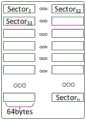
所述的面向图神经网络应用的片上存储方法,其中SPM以区块的形式组织数据,每个区块存储64Byte的数据,并以起始地址和向量数据长度完成存储向量数据的多个区块的连续访问。The described on-chip storage method for graph neural network application, wherein SPM organizes data in the form of blocks, each block stores 64Byte data, and completes multiple blocks storing vector data with starting address and vector data length continuous access.
本发明还提出了一种面向图神经网络应用的片上存储系统,其中包括:The present invention also proposes an on-chip storage system oriented to graph neural network applications, which includes:
模块1、根据处理单元对图神经网络模型中向量数据的访存请求,判断在片上存储系统的第一级CAM结构中是否有于该访存请求对应的查询结果,若有则执行模块2,否则判断在片上存储系统的第二级CAM结构中是否有于该访存请求对应的查询结果,若有则执行模块2,否则根据所需的向量数据批量对片外存储器发起片外访存请求,并替换片上存储内的指定向量数据;
模块2、根据该查询结果,得到对应的SPM索引标记,利用该SPM索引标记中的SectorIndex字段以向量方式访问SPM中的相应向量数据,并将该相应数据返回给处理单元。Module 2: Obtain the corresponding SPM index mark according to the query result, use the SectorIndex field in the SPM index mark to access the corresponding vector data in the SPM in a vector manner, and return the corresponding data to the processing unit.
所述的面向图神经网络应用的片上存储系统,其中该第一级CAM结构和该第二级CAM结构中的每个条目均包含:查询标签和SPM索引标记;The on-chip storage system for graph neural network applications, wherein each entry in the first-level CAM structure and the second-level CAM structure includes: a query tag and an SPM index tag;
该查询标签用于查询SPM索引标记,包含:用于区分图神经网络不同阶段的场景编号MID;聚合/输出特征向量的节点编号VID或输入特征向量的邻居节点编号NeiID或权重矩阵的行编号RowID。This query tag is used to query the SPM index tag, including: scene number MID used to distinguish different stages of graph neural network; node number VID of aggregation/output feature vector or neighbor node number NeiID of input feature vector or row number RowID of weight matrix .
该SPM索引标记包含:SPM数据替换提示标记与记录SPM数据首地址的区块编号。The SPM index mark includes: the SPM data replacement prompt mark and the block number for recording the first address of the SPM data.
所述的面向图神经网络应用的片上存储系统,其中以向量方式访问SPM中的相应向量数据包括:连续访问以SectorIndex作为起始访存地址且以被访问向量数据的长度作为访存长度的片上存储空间。The described on-chip storage system for graph neural network applications, wherein accessing corresponding vector data in the SPM in a vector manner comprises: continuously accessing the on-chip with SectorIndex as the starting memory access address and the length of the accessed vector data as the memory access length. storage.
所述的面向图神经网络应用的片上存储系统,其中The on-chip storage system for graph neural network applications, wherein
在SPM中分配预设值以下的第一存储空间用于存储多层感知器的参数;Allocate the first storage space below the preset value in the SPM for storing the parameters of the multilayer perceptron;
在SPM中根据聚合运算后得到的特征向量长度以及当前在线处理的节点数量分配第二存储空间,用于存储聚合后的特征向量、多层感知器输出的特征向量;In the SPM, a second storage space is allocated according to the length of the feature vector obtained after the aggregation operation and the number of nodes currently processed online, for storing the feature vector after the aggregation and the feature vector output by the multilayer perceptron;
在SPM中除去该第一存储空间和该第二存储空间以外的存储空间,用于缓存在图遍历期间产生数据替换的输入特征向量。Storage spaces other than the first storage space and the second storage space are removed in the SPM for caching input feature vectors that generate data replacements during graph traversal.
所述的面向图神经网络应用的片上存储系统,其中SPM以区块的形式组织数据,每个区块存储64Byte的数据,并以起始地址和向量数据长度完成存储向量数据的多个区块的连续访问。The described on-chip storage system for graph neural network application, wherein SPM organizes data in the form of blocks, each block stores 64Byte data, and completes multiple blocks for storing vector data with starting address and vector data length continuous access.
由以上方案可知,本发明的优点在于:As can be seen from the above scheme, the advantages of the present invention are:
(1)本发明采用两级CAM(内容可寻址存储器Content Addressed Memory),结构与SPM(便笺式存储器Scratch Pad Memory)存储单元结合的方式,支持图神经网络不同阶段统一使用相同的片上存储资源,能够动态进行存储划分,有效提升片上存储资源的利用率和访存通量;(1) The present invention adopts two-level CAM (Content Addressed Memory), the structure is combined with the SPM (Scratch Pad Memory) storage unit, and supports the unified use of the same on-chip storage resources in different stages of the graph neural network , which can dynamically divide storage to effectively improve the utilization of on-chip storage resources and memory access throughput;
(2)本发明中片上存储系统的SPM采用区块sector的形式组织数据并以向量方式访问数据,增强数据存储灵活性,便于进行动态存储划分,以及提高访存通量;(2) The SPM of the on-chip storage system in the present invention organizes data in the form of block sectors and accesses data in a vector mode, which enhances the flexibility of data storage, facilitates dynamic storage division, and improves memory access throughput;
(3)本发明中片上存储系统的两级CAM结构,高效索引SPM中内容,且支持以较小开销动态根据存储划分进行信息重配。(3) The two-level CAM structure of the on-chip storage system in the present invention efficiently indexes the content in the SPM, and supports dynamic information reconfiguration according to storage division with less overhead.
附图说明Description of drawings
图1为单级CAM结构示意图;Figure 1 is a schematic diagram of a single-stage CAM structure;
图2为SPM存储单元结构示意图;Fig. 2 is a structural schematic diagram of an SPM storage unit;
图3为片上存储系统访存示意图。FIG. 3 is a schematic diagram of memory access of an on-chip storage system.
具体实施方式Detailed ways
本发明设计一种面向图神经网络应用的片上存储系统。该系统包含一块用于存储片上图数据的SPM(Scratch Pad Memory),以及用于检索SPM中数据的两级CAM结构。本发明利用动态可重配等策略支持图神经网络系统的不同阶段统一使用片上存储,提升存储资源利用率与访存通量。The invention designs an on-chip storage system oriented to graph neural network application. The system includes a SPM (Scratch Pad Memory) for storing on-chip image data, and a two-level CAM structure for retrieving data in the SPM. The present invention utilizes strategies such as dynamic reconfiguration to support the unified use of on-chip storage in different stages of the graph neural network system, thereby improving storage resource utilization and memory access throughput.
1.两级CAM结构1. Two-level CAM structure
本发明的片上存储系统中包含用于检索SPM中数据的两级CAM结构,结构示意图参见附图1。该两级CAM结构通过动态可重配性实现片上存储动态分割,从而有效地利用片上存储,满足图神经网络不同阶段执行过程中变化的存储需求。动态可重配性具体过程是将被各个存储空间存储的向量数据的条目写入到CAM结构中,向量数据存储到SPM存储单元中。比如分配第二存储空间的过程中,每个节点的向量数据的节点编号、MID和sectorindex作为一个条目,写入CAM结构中,向量数据根据sectorindex写入到SPM中。The on-chip storage system of the present invention includes a two-level CAM structure for retrieving data in the SPM, and a schematic diagram of the structure is shown in FIG. 1 . The two-level CAM structure realizes dynamic segmentation of on-chip storage through dynamic reconfigurability, thereby effectively utilizing on-chip storage and meeting the changing storage requirements during the execution of different stages of the graph neural network. The specific process of dynamic reconfigurability is to write the entries of the vector data stored in each storage space into the CAM structure, and store the vector data into the SPM storage unit. For example, in the process of allocating the second storage space, the node number, MID and sectorindex of the vector data of each node are written into the CAM structure as an entry, and the vector data is written into the SPM according to the sectorindex.
第一级CAM用于检索SPM中最经常访问的数据,当有数据访存请求输入时,第一级CAM首先进行查询,如果发生缺失,则立即进行第二级CAM的查询。两级结构能够有效降低较大的单级(二级)CAM的查询开销。如附图1所示,CAM中的每个条目都包含两块内容:查询标签和SPM索引标记。查询标签用于查询SPM索引标记,包含两部分内容:用于区分图神经网络不同阶段的场景编号MID;聚合/输出特征向量的节点编号VID或输入特征向量的邻居节点编号NeiID或权重矩阵的行编号RowID。SPM索引标记包含两部分内容:SPM数据替换提示标记与记录SPM数据首地址的区块编号(Sector Index)。The first-level CAM is used to retrieve the most frequently accessed data in the SPM. When a data fetch request is input, the first-level CAM will query first, and if there is a missing, the second-level CAM will be queried immediately. The two-level structure can effectively reduce the query cost of a large single-level (two-level) CAM. As shown in Figure 1, each entry in the CAM contains two pieces of content: the query tag and the SPM index tag. The query tag is used to query the SPM index tag, which contains two parts: the scene number MID used to distinguish different stages of the graph neural network; the node number VID of the aggregation/output feature vector or the neighbor node number of the input feature vector NeiID or the row of the weight matrix Number RowID. The SPM index mark contains two parts: the SPM data replacement prompt mark and the block number (Sector Index) that records the first address of the SPM data.
存储单元需对四种不同类型的数据进行存储空间划分。在Aggregation阶段,SPM存储单元中仅缓存输入的节点特征向量以及聚合运算后得到的特征向量;在Combination阶段,SPM存储单元缓存聚合后的特征向量、多层感知器(Multi-layered perceptron,MLP)的参数以及输出的特征向量。如附图1所示,对应于上述四种不同类型数据,每个SPM索引标记可用于索引不同类型的数据,具体内容为:InFVAddr包含输入特征向量的地址和记录输入特征向量中剩余未处理出度的ReOutDeg,即数据替换指示标记;OutFVAddr包含输出特征向量的地址;AggFVAddr包含聚合后特征向量的地址;WRowAddr包含权重矩阵的行地址。The storage unit needs to divide the storage space for four different types of data. In the Aggregation stage, only the input node feature vector and the feature vector obtained after the aggregation operation are cached in the SPM storage unit; in the Combination stage, the SPM storage unit caches the aggregated feature vector, Multi-layered perceptron (MLP) parameters and the output eigenvectors. As shown in FIG. 1, corresponding to the above-mentioned four different types of data, each SPM index mark can be used to index different types of data, and the specific content is: InFVAddr contains the address of the input feature vector and records the remaining unprocessed data in the input feature vector. ReOutDeg of degree, that is, the data replacement indicator; OutFVAddr contains the address of the output feature vector; AggFVAddr contains the address of the aggregated feature vector; WRowAddr contains the row address of the weight matrix.
2.SPM存储单元2. SPM storage unit
如附图2所示,为方便数据重置,本发明片上存储系统中的SPM以一系列区块(sector)的形式组织数据,每个区块可以存储64Byte的数据。由于在图神经网络模型的单个层/迭代中,特征向量的长度和权重矩阵行的尺寸是确定的,因此特征数据和权重参数可存储于连续的若干区块中,且仅需用一个地址来索引起始区块即可。As shown in FIG. 2 , in order to facilitate data reset, the SPM in the on-chip storage system of the present invention organizes data in the form of a series of sectors, and each sector can store 64 Bytes of data. Since the length of the feature vector and the size of the weight matrix row are determined in a single layer/iteration of the graph neural network model, the feature data and weight parameters can be stored in consecutive blocks, and only one address is needed to The index start block is sufficient.
SPM中存储空间分配规则如下:1)对于多层感知器的参数,仅需分配较小的固定存储空间;2)对于聚合后的以及输出的特征向量,存储空间分配取决于这些特征向量的长度以及当前在线处理的节点数量;3)剩余的存储空间可用于缓存在图遍历期间产生数据替换的输入特征向量。在运行时,本系统能够动态地将大型SPM存储进行分割,分配给不同类型的数据,并且只需很小的开销即可根据存储需求调整CAM结构中的相应条目。The storage space allocation rules in SPM are as follows: 1) For the parameters of the multi-layer perceptron, only a small fixed storage space needs to be allocated; 2) For the aggregated and output feature vectors, the storage space allocation depends on the length of these feature vectors and the number of nodes currently processed online; 3) the remaining storage space can be used to cache the input feature vectors that generate data replacement during graph traversal. At runtime, the system can dynamically partition large SPM storage to different types of data, and adjust the corresponding entries in the CAM structure according to storage requirements with little overhead.
为让本发明的上述特征和效果能阐述的更明确易懂,下文特举实施例,并配合说明书附图作详细说明如下。In order to make the above-mentioned features and effects of the present invention more clearly and comprehensible, embodiments are given below, and detailed descriptions are given below in conjunction with the accompanying drawings.
本发明针对图神经网络应用中不同阶段变化的访存需求特性,设计统一的片上存储系统,利用两级CAM结构与SPM的构架方式灵活地组织和检索片上图数据,同时通过动态可重配性有效提升存储资源利用率和访存通量。Aiming at the characteristics of memory access requirements that change at different stages in the application of the graph neural network, the present invention designs a unified on-chip storage system, utilizes the two-level CAM structure and the SPM framework to flexibly organize and retrieve the on-chip graph data, and at the same time, through the dynamic reconfigurability Effectively improve storage resource utilization and memory access throughput.
下面从具体示例对本发明的具体实施方式进行进一步说明。The specific embodiments of the present invention will be further described below from specific examples.
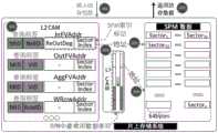
附图3为该片上存储系统的访存过程示意图。在图神经网络模型访存过程中,片上存储系统根据输入的节点编号或邻居节点编号,以及用于区分图神经网络不同阶段的场景编号MID在两级CAM结构中对被访问的向量数据的存储起始地址进行查询,得到SPM中对应向量数据的起始sector地址和数据替换指示标记,并将连续多个sector内的数据返回给处理单元,具体步骤如下:FIG. 3 is a schematic diagram of a memory access process of the on-chip storage system. During the memory access process of the graph neural network model, the on-chip storage system stores the accessed vector data in the two-level CAM structure according to the input node number or neighbor node number, as well as the scene number MID used to distinguish different stages of the graph neural network. The starting address is queried to obtain the starting sector address and data replacement indicator of the corresponding vector data in the SPM, and the data in multiple consecutive sectors is returned to the processing unit. The specific steps are as follows:
步骤301:片上存储系统接收输入的访存请求,请求内容包含了节点编号或邻居节点编号,以及用于区分图神经网络不同阶段的场景编号MID;Step 301: the on-chip storage system receives the input memory access request, and the request content includes the node number or the neighbor node number, and the scene number MID used to distinguish different stages of the graph neural network;
步骤302:根据请求信息,首先在第一级CAM结构(L1CAM)中进行查询;Step 302: According to the request information, first query in the first-level CAM structure (L1CAM);
步骤303:若L1CAM无法索引得到向量数据的访存起始sector地址,则在第二级CAM结构(L2CAM)中进行查询;Step 303: If the L1CAM cannot obtain the starting sector address of the memory access of the vector data by indexing, query in the second-level CAM structure (L2CAM);
步骤304:根据L1/L2CAM的查询结果,得到对应的SPM索引标记,利用其中的SectorIndex字段连续访问SPM中相应多个sector的数据,以完成向量数据的访问;Step 304: Obtain the corresponding SPM index mark according to the query result of the L1/L2CAM, and use the SectorIndex field therein to continuously access the data of the corresponding multiple sectors in the SPM to complete the access of the vector data;
步骤305:SPM返回所需向量数据给处理单元;Step 305: SPM returns the required vector data to the processing unit;
步骤306:若两级CAM的查询均失败,则SPM需要片外访存进行数据替换。SPM存储单元根据SPM中所有输入特征向量的数据替换指示标记,选择剩余未处理出度最小的输入特征向量,批量对片外存储器发起片外访存请求,并替换该向量数据。Step 306: If the query of the two-level CAM fails, the SPM needs to fetch the off-chip memory to perform data replacement. According to the data replacement indicator of all input feature vectors in the SPM, the SPM storage unit selects the input feature vector with the smallest remaining unprocessed out-degree, initiates off-chip memory access requests to the off-chip memory in batches, and replaces the vector data.
上述访存方式不是用地址访存,而是通过CAM中节点编号等信息首先索引获取SPM索引项,然后通过SPM索引项访问SPM存储器中数据。由此可以体现出本申请面向的是图数据的访存过程。The above-mentioned memory fetching method does not use address fetching, but firstly obtains the SPM index entry by indexing through information such as the node number in the CAM, and then accesses the data in the SPM memory through the SPM index entry. Therefore, it can be shown that the present application is directed to the process of accessing graph data.
Claims (10)
Priority Applications (1)
| Application Number | Priority Date | Filing Date | Title |
|---|---|---|---|
| CN202010395809.4ACN111695685B (en) | 2020-05-12 | 2020-05-12 | On-chip storage system and method for graph neural network application |
Applications Claiming Priority (1)
| Application Number | Priority Date | Filing Date | Title |
|---|---|---|---|
| CN202010395809.4ACN111695685B (en) | 2020-05-12 | 2020-05-12 | On-chip storage system and method for graph neural network application |
Publications (2)
| Publication Number | Publication Date |
|---|---|
| CN111695685Atrue CN111695685A (en) | 2020-09-22 |
| CN111695685B CN111695685B (en) | 2023-09-26 |
Family
ID=72477607
Family Applications (1)
| Application Number | Title | Priority Date | Filing Date |
|---|---|---|---|
| CN202010395809.4AActiveCN111695685B (en) | 2020-05-12 | 2020-05-12 | On-chip storage system and method for graph neural network application |
Country Status (1)
| Country | Link |
|---|---|
| CN (1) | CN111695685B (en) |
Cited By (1)
| Publication number | Priority date | Publication date | Assignee | Title |
|---|---|---|---|---|
| CN114239816A (en)* | 2021-12-09 | 2022-03-25 | 电子科技大学 | Reconfigurable hardware acceleration architecture of convolutional neural network-graph convolutional neural network |
Citations (5)
| Publication number | Priority date | Publication date | Assignee | Title |
|---|---|---|---|---|
| US4038537A (en)* | 1975-12-22 | 1977-07-26 | Honeywell Information Systems, Inc. | Apparatus for verifying the integrity of information stored in a data processing system memory |
| WO2014190695A1 (en)* | 2013-05-31 | 2014-12-04 | 华为技术有限公司 | Memory system, memory access request processing method and computer system |
| WO2017156968A1 (en)* | 2016-03-16 | 2017-09-21 | 中国科学院计算技术研究所 | Neural network computing method, system and device therefor |
| CN108959384A (en)* | 2018-05-31 | 2018-12-07 | 康键信息技术(深圳)有限公司 | Web data acquisition methods, device, computer equipment and storage medium |
| US20190087716A1 (en)* | 2016-04-18 | 2019-03-21 | Institute Of Computing Technology, Chinese Academy Of Sciences | Method and system for processing neural network |
- 2020
- 2020-05-12CNCN202010395809.4Apatent/CN111695685B/enactiveActive
Patent Citations (5)
| Publication number | Priority date | Publication date | Assignee | Title |
|---|---|---|---|---|
| US4038537A (en)* | 1975-12-22 | 1977-07-26 | Honeywell Information Systems, Inc. | Apparatus for verifying the integrity of information stored in a data processing system memory |
| WO2014190695A1 (en)* | 2013-05-31 | 2014-12-04 | 华为技术有限公司 | Memory system, memory access request processing method and computer system |
| WO2017156968A1 (en)* | 2016-03-16 | 2017-09-21 | 中国科学院计算技术研究所 | Neural network computing method, system and device therefor |
| US20190087716A1 (en)* | 2016-04-18 | 2019-03-21 | Institute Of Computing Technology, Chinese Academy Of Sciences | Method and system for processing neural network |
| CN108959384A (en)* | 2018-05-31 | 2018-12-07 | 康键信息技术(深圳)有限公司 | Web data acquisition methods, device, computer equipment and storage medium |
Non-Patent Citations (6)
| Title |
|---|
| GUANHUA WANG等: "Data Allocation for Embedded Systems with Hybrid On-Chip Scratchpad and Caches", 《2013 IEEE INTERNATIONAL CONFERENCE ON HIGH PERFORMANCE COMPUTING AND COMMUNICATIONS & 2013 IEEE INTERNATIONAL CONFERENCE ON EMBEDDED AND UBIQUITOUS COMPUTING》* |
| GUANHUA WANG等: "Data Allocation for Embedded Systems with Hybrid On-Chip Scratchpad and Caches", 《2013 IEEE INTERNATIONAL CONFERENCE ON HIGH PERFORMANCE COMPUTING AND COMMUNICATIONS & 2013 IEEE INTERNATIONAL CONFERENCE ON EMBEDDED AND UBIQUITOUS COMPUTING》, 12 June 2014 (2014-06-12), pages 366 - 373* |
| 张旭等: "面向图计算应用的处理器访存通路优化设计与实现", 《国防科技大学学报》* |
| 张旭等: "面向图计算应用的处理器访存通路优化设计与实现", 《国防科技大学学报》, vol. 42, no. 02, 28 April 2020 (2020-04-28), pages 13 - 22* |
| 曾成龙: "面向嵌入式 FPGA 的高性能卷积神经网络加速器设计", 《计算机辅助设计与图形学学报》* |
| 曾成龙: "面向嵌入式 FPGA 的高性能卷积神经网络加速器设计", 《计算机辅助设计与图形学学报》, vol. 31, no. 9, 30 September 2019 (2019-09-30), pages 1645 - 1652* |
Cited By (2)
| Publication number | Priority date | Publication date | Assignee | Title |
|---|---|---|---|---|
| CN114239816A (en)* | 2021-12-09 | 2022-03-25 | 电子科技大学 | Reconfigurable hardware acceleration architecture of convolutional neural network-graph convolutional neural network |
| CN114239816B (en)* | 2021-12-09 | 2023-04-07 | 电子科技大学 | Reconfigurable hardware acceleration architecture of convolutional neural network-graph convolutional neural network |
Also Published As
| Publication number | Publication date |
|---|---|
| CN111695685B (en) | 2023-09-26 |
Similar Documents
| Publication | Publication Date | Title |
|---|---|---|
| JP6662990B2 (en) | System and method for modeling an object network | |
| CN107423368B (en) | Spatio-temporal data indexing method in non-relational database | |
| JP6356675B2 (en) | Aggregation / grouping operation: Hardware implementation of hash table method | |
| US10296462B2 (en) | Method to accelerate queries using dynamically generated alternate data formats in flash cache | |
| CN104361113B (en) | A kind of OLAP query optimization method under internal memory flash memory mixing memory module | |
| CN1955948A (en) | Digital data processing device and method for managing cache data | |
| CN112000846A (en) | A method for grouping LSM tree index based on GPU | |
| CN114637700B (en) | Address translation method for target virtual address, processor and electronic equipment | |
| CN111429974B (en) | Molecular dynamics simulation short-range force parallel optimization method on super computer platform | |
| CN102663115A (en) | Main memory database access optimization method on basis of page coloring technology | |
| CN1831824A (en) | Cache database data organization method | |
| CN110795363A (en) | Hot page prediction method and page scheduling method for storage medium | |
| CN103942301B (en) | Distributed file system oriented to access and application of multiple data types | |
| CN114356893A (en) | Metadata tuning method, device, equipment and storage medium based on machine learning | |
| CN116401502B (en) | A method and device for optimizing Winograd convolution based on NUMA system characteristics | |
| CN106055679A (en) | Multi-level cache sensitive indexing method | |
| CN114078143A (en) | Coherence gathering for ray tracing | |
| CN117763008A (en) | Data sorting method and device | |
| CN111695685B (en) | On-chip storage system and method for graph neural network application | |
| WO2015032214A1 (en) | High-speed routing lookup method and device simultaneously supporting ipv4 and ipv6 | |
| CN115203211A (en) | A method and system for generating a unique hash sequence number | |
| CN118193540A (en) | Index processing method, device, electronic device and readable storage medium | |
| CN1896972A (en) | Method and device for converting virtual address, reading and writing high-speed buffer memory | |
| CN115129233B (en) | Data processing devices, methods and related products | |
| CN107526528B (en) | Mechanism for realizing on-chip low-delay memory |
Legal Events
| Date | Code | Title | Description |
|---|---|---|---|
| PB01 | Publication | ||
| PB01 | Publication | ||
| SE01 | Entry into force of request for substantive examination | ||
| SE01 | Entry into force of request for substantive examination | ||
| GR01 | Patent grant | ||
| GR01 | Patent grant |