CN111684772B - Synchronous switching multiple-input demodulation comparator - Google Patents
Synchronous switching multiple-input demodulation comparatorDownload PDFInfo
- Publication number
- CN111684772B CN111684772BCN201880084127.2ACN201880084127ACN111684772BCN 111684772 BCN111684772 BCN 111684772BCN 201880084127 ACN201880084127 ACN 201880084127ACN 111684772 BCN111684772 BCN 111684772B
- Authority
- CN
- China
- Prior art keywords
- carrier modulation
- pair
- transistors
- signal
- transistor
- Prior art date
- Legal status (The legal status is an assumption and is not a legal conclusion. Google has not performed a legal analysis and makes no representation as to the accuracy of the status listed.)
- Active
Links
Images


Classifications
- H—ELECTRICITY
- H04—ELECTRIC COMMUNICATION TECHNIQUE
- H04L—TRANSMISSION OF DIGITAL INFORMATION, e.g. TELEGRAPHIC COMMUNICATION
- H04L25/00—Baseband systems
- H04L25/02—Details ; arrangements for supplying electrical power along data transmission lines
- H04L25/0264—Arrangements for coupling to transmission lines
- H04L25/0272—Arrangements for coupling to multiple lines, e.g. for differential transmission
- H—ELECTRICITY
- H04—ELECTRIC COMMUNICATION TECHNIQUE
- H04L—TRANSMISSION OF DIGITAL INFORMATION, e.g. TELEGRAPHIC COMMUNICATION
- H04L27/00—Modulated-carrier systems
- H04L27/26—Systems using multi-frequency codes
- H04L27/2601—Multicarrier modulation systems
- H—ELECTRICITY
- H03—ELECTRONIC CIRCUITRY
- H03L—AUTOMATIC CONTROL, STARTING, SYNCHRONISATION OR STABILISATION OF GENERATORS OF ELECTRONIC OSCILLATIONS OR PULSES
- H03L7/00—Automatic control of frequency or phase; Synchronisation
- H03L7/06—Automatic control of frequency or phase; Synchronisation using a reference signal applied to a frequency- or phase-locked loop
- H03L7/08—Details of the phase-locked loop
- H03L7/099—Details of the phase-locked loop concerning mainly the controlled oscillator of the loop
- H03L7/0991—Details of the phase-locked loop concerning mainly the controlled oscillator of the loop the oscillator being a digital oscillator, e.g. composed of a fixed oscillator followed by a variable frequency divider
- H03L7/0992—Details of the phase-locked loop concerning mainly the controlled oscillator of the loop the oscillator being a digital oscillator, e.g. composed of a fixed oscillator followed by a variable frequency divider comprising a counter or a frequency divider
- H—ELECTRICITY
- H04—ELECTRIC COMMUNICATION TECHNIQUE
- H04L—TRANSMISSION OF DIGITAL INFORMATION, e.g. TELEGRAPHIC COMMUNICATION
- H04L25/00—Baseband systems
- H04L25/02—Details ; arrangements for supplying electrical power along data transmission lines
- H04L25/0264—Arrangements for coupling to transmission lines
- H04L25/0272—Arrangements for coupling to multiple lines, e.g. for differential transmission
- H04L25/0274—Arrangements for ensuring balanced coupling
- H—ELECTRICITY
- H04—ELECTRIC COMMUNICATION TECHNIQUE
- H04L—TRANSMISSION OF DIGITAL INFORMATION, e.g. TELEGRAPHIC COMMUNICATION
- H04L25/00—Baseband systems
- H04L25/02—Details ; arrangements for supplying electrical power along data transmission lines
- H04L25/0264—Arrangements for coupling to transmission lines
- H04L25/0292—Arrangements specific to the receiver end
- H—ELECTRICITY
- H04—ELECTRIC COMMUNICATION TECHNIQUE
- H04L—TRANSMISSION OF DIGITAL INFORMATION, e.g. TELEGRAPHIC COMMUNICATION
- H04L25/00—Baseband systems
- H04L25/38—Synchronous or start-stop systems, e.g. for Baudot code
- H04L25/40—Transmitting circuits; Receiving circuits
- H04L25/49—Transmitting circuits; Receiving circuits using code conversion at the transmitter; using predistortion; using insertion of idle bits for obtaining a desired frequency spectrum; using three or more amplitude levels ; Baseband coding techniques specific to data transmission systems
- H04L25/4917—Transmitting circuits; Receiving circuits using code conversion at the transmitter; using predistortion; using insertion of idle bits for obtaining a desired frequency spectrum; using three or more amplitude levels ; Baseband coding techniques specific to data transmission systems using multilevel codes
- H04L25/4919—Transmitting circuits; Receiving circuits using code conversion at the transmitter; using predistortion; using insertion of idle bits for obtaining a desired frequency spectrum; using three or more amplitude levels ; Baseband coding techniques specific to data transmission systems using multilevel codes using balanced multilevel codes
- H—ELECTRICITY
- H04—ELECTRIC COMMUNICATION TECHNIQUE
- H04L—TRANSMISSION OF DIGITAL INFORMATION, e.g. TELEGRAPHIC COMMUNICATION
- H04L27/00—Modulated-carrier systems
- H04L27/10—Frequency-modulated carrier systems, i.e. using frequency-shift keying
- H04L27/14—Demodulator circuits; Receiver circuits
- H04L27/144—Demodulator circuits; Receiver circuits with demodulation using spectral properties of the received signal, e.g. by using frequency selective- or frequency sensitive elements
- H04L27/148—Demodulator circuits; Receiver circuits with demodulation using spectral properties of the received signal, e.g. by using frequency selective- or frequency sensitive elements using filters, including PLL-type filters
- H—ELECTRICITY
- H04—ELECTRIC COMMUNICATION TECHNIQUE
- H04L—TRANSMISSION OF DIGITAL INFORMATION, e.g. TELEGRAPHIC COMMUNICATION
- H04L27/00—Modulated-carrier systems
- H04L27/18—Phase-modulated carrier systems, i.e. using phase-shift keying
- H04L27/20—Modulator circuits; Transmitter circuits
- H04L27/2032—Modulator circuits; Transmitter circuits for discrete phase modulation, e.g. in which the phase of the carrier is modulated in a nominally instantaneous manner
- H04L27/2053—Modulator circuits; Transmitter circuits for discrete phase modulation, e.g. in which the phase of the carrier is modulated in a nominally instantaneous manner using more than one carrier, e.g. carriers with different phases
- H04L27/206—Modulator circuits; Transmitter circuits for discrete phase modulation, e.g. in which the phase of the carrier is modulated in a nominally instantaneous manner using more than one carrier, e.g. carriers with different phases using a pair of orthogonal carriers, e.g. quadrature carriers
- H04L27/2067—Modulator circuits; Transmitter circuits for discrete phase modulation, e.g. in which the phase of the carrier is modulated in a nominally instantaneous manner using more than one carrier, e.g. carriers with different phases using a pair of orthogonal carriers, e.g. quadrature carriers with more than two phase states
- H04L27/2071—Modulator circuits; Transmitter circuits for discrete phase modulation, e.g. in which the phase of the carrier is modulated in a nominally instantaneous manner using more than one carrier, e.g. carriers with different phases using a pair of orthogonal carriers, e.g. quadrature carriers with more than two phase states in which the data are represented by the carrier phase, e.g. systems with differential coding
- H—ELECTRICITY
- H04—ELECTRIC COMMUNICATION TECHNIQUE
- H04L—TRANSMISSION OF DIGITAL INFORMATION, e.g. TELEGRAPHIC COMMUNICATION
- H04L27/00—Modulated-carrier systems
- H04L27/26—Systems using multi-frequency codes
- H04L27/2601—Multicarrier modulation systems
- H04L27/2602—Signal structure
- H—ELECTRICITY
- H04—ELECTRIC COMMUNICATION TECHNIQUE
- H04L—TRANSMISSION OF DIGITAL INFORMATION, e.g. TELEGRAPHIC COMMUNICATION
- H04L27/00—Modulated-carrier systems
- H04L27/26—Systems using multi-frequency codes
- H04L27/2601—Multicarrier modulation systems
- H04L27/2602—Signal structure
- H04L27/2605—Symbol extensions, e.g. Zero Tail, Unique Word [UW]
- H—ELECTRICITY
- H04—ELECTRIC COMMUNICATION TECHNIQUE
- H04L—TRANSMISSION OF DIGITAL INFORMATION, e.g. TELEGRAPHIC COMMUNICATION
- H04L7/00—Arrangements for synchronising receiver with transmitter
- H04L7/02—Speed or phase control by the received code signals, the signals containing no special synchronisation information
- H04L7/033—Speed or phase control by the received code signals, the signals containing no special synchronisation information using the transitions of the received signal to control the phase of the synchronising-signal-generating means, e.g. using a phase-locked loop
- H—ELECTRICITY
- H04—ELECTRIC COMMUNICATION TECHNIQUE
- H04L—TRANSMISSION OF DIGITAL INFORMATION, e.g. TELEGRAPHIC COMMUNICATION
- H04L27/00—Modulated-carrier systems
- H04L27/0014—Carrier regulation
- H04L2027/0024—Carrier regulation at the receiver end
- H04L2027/0026—Correction of carrier offset
- H04L2027/0036—Correction of carrier offset using a recovered symbol clock
- H—ELECTRICITY
- H04—ELECTRIC COMMUNICATION TECHNIQUE
- H04L—TRANSMISSION OF DIGITAL INFORMATION, e.g. TELEGRAPHIC COMMUNICATION
- H04L2201/00—Algorithms used for the adjustment of time-domain equalizers
- H04L2201/04—Algorithms used for the adjustment of time-domain equalizers zero-forcing
Landscapes
- Engineering & Computer Science (AREA)
- Computer Networks & Wireless Communication (AREA)
- Signal Processing (AREA)
- Power Engineering (AREA)
- Physics & Mathematics (AREA)
- Spectroscopy & Molecular Physics (AREA)
- Digital Transmission Methods That Use Modulated Carrier Waves (AREA)
- Dc Digital Transmission (AREA)
Abstract
Translated fromChinese
Description
Translated fromChinese相关申请的交叉引用Cross References to Related Applications
本申请要求申请号为62/611,523,申请日为2017年12月28日,发明人为ArminTajalli,名称为“组合型多输入比较器/解调器”的美国临时申请的权益,并通过引用将其内容整体并入本文,以供所有目的之用。This application claims the benefit of U.S. Provisional Application No. 62/611,523, filed December 28, 2017, inventor Armin Tajalli, entitled "Combined Multiple-Input Comparator/Demodulator," which is hereby incorporated by reference The content is incorporated herein in its entirety for all purposes.
参考文献references
以下参考文献通过引用整体并入本文,以供所有目的之用:The following references are hereby incorporated by reference in their entirety for all purposes:
公开号为2011/0268225,申请号为12/784,414,申请日为2010年5月20日,发明人为Harm Cronie和Amin Shokrollahi,名称为“正交差分向量信令”的美国专利申请,下称《Cronie1》;The publication number is 2011/0268225, the application number is 12/784,414, the application date is May 20, 2010, the inventors are Harm Cronie and Amin Shokrollahi, the U.S. patent application titled "Orthogonal Differential Vector Signaling", hereinafter referred to as " Cronie1";
申请号为13/030,027,申请日为2011年2月17日,发明人为Harm Cronie,AminShokrollahi及Armin Tajalli,名称为“利用稀疏信令码进行抗噪声干扰、高引脚利用率、低功耗通讯的方法和系统”的美国专利申请,下称《Cronie 2》;The application number is 13/030,027, the application date is February 17, 2011, the inventors are Harm Cronie, AminShokrollahi and Armin Tajalli, and the name is "Using sparse signaling codes for anti-noise interference, high pin utilization, and low power consumption communication method and system for ", hereinafter referred to as "Cronie 2";
申请号为14/158,452,申请日为2014年1月17日,发明人为John Fox、BrianHolden、Peter Hunt、John D Keay、Amin Shokrollahi、Richard Simpson、Anant Singh、Andrew Kevin John Stewart和Giuseppe Surace,名称为“低SSO噪声芯片间通信方法和系统”的美国专利申请,下称《Fox 1》;Application No. 14/158,452, filed January 17, 2014, inventors John Fox, Brian Holden, Peter Hunt, John D Keay, Amin Shokrollahi, Richard Simpson, Anant Singh, Andrew Kevin John Stewart, and Giuseppe Surace, named US patent application for "Low SSO Noise Inter-Chip Communication Method and System", hereinafter referred to as "Fox 1";
申请号为13/842,740,申请日为2013年3月15日,发明人为Brian Holden、AminShokrollahi和Anant Singh,名称为“芯片间通信用向量信令码的时偏耐受方法和系统以及增强型检测器”的美国专利申请,下称《Holden 1》;The application number is 13/842,740, the filing date is March 15, 2013, the inventors are Brian Holden, AminShokrollahi and Anant Singh, and the title is "Time skew tolerant method and system of vector signaling code for inter-chip communication and enhanced detection device", hereinafter referred to as "Holden 1";
申请号为61/934,804,申请日为2014年2月2日,发明人为Ali Hormati和AminShokrollahi,名称为“以ISI比评价代码的方法”的美国临时专利申请,下称《Hormati 1》;The application number is 61/934,804, the filing date is February 2, 2014, the inventors are Ali Hormati and AminShokrollahi, and the U.S. provisional patent application titled "Method for evaluating codes by ISI ratio", hereinafter referred to as "Hormati 1";
申请号为62/026,860,申请日为2014年7月21日,发明人为Ali Hormati和AminShokrollahi,名称为“多点数据传输”的美国临时专利申请,下称《Hormati 2》;Application No. 62/026,860, dated July 21, 2014, inventors Ali Hormati and AminShokrollahi, U.S. Provisional Patent Application entitled "Multipoint Data Transmission", hereinafter referred to as "Hormati 2";
申请号为15/194,497,申请日为2016年6月27日,发明人为Ali Hormati、ArminTajalli和Amin Shokrollahi,名称为“高速芯片间通信用方法和装置”的美国专利申请,下称《Hormati 3》;The application number is 15/194,497, the filing date is June 27, 2016, the inventors are Ali Hormati, Armin Tajalli and Amin Shokrollahi, and the U.S. patent application titled "Method and device for high-speed inter-chip communication", hereinafter referred to as "Hormati 3" ;
申请号为15/802,365,申请日为2017年11月2日,发明人为Ali Hormati和ArminTajalli,名称为“多通道数据接收器的时钟数据恢复”的美国专利申请,下称《Hormati 4》;The application number is 15/802,365, the filing date is November 2, 2017, the inventors are Ali Hormati and Armin Tajalli, the United States patent application titled "Clock Data Recovery for Multi-Channel Data Receiver", hereinafter referred to as "Hormati 4";
申请号为61/934,807,申请日为2014年2月2日,发明人为Amin Shokrollahi,名称为“高引脚利用率向量信令码及其在芯片间通信及存储中的应用”的美国临时专利申请,下称《Shokrollahi 1》;The application number is 61/934,807, the filing date is February 2, 2014, the inventor is Amin Shokrollahi, and the U.S. provisional patent titled "High Pin Utilization Vector Signaling Code and Its Application in Inter-chip Communication and Storage" Application, hereinafter "Shokrollahi 1";
申请号为61/839,360,申请日为2013年6月23日,发明人为Amin Shokrollahi,名称为“低接收器复杂度向量信令码”的美国临时专利申请,下称《Shokrollahi 2》;The application number is 61/839,360, the filing date is June 23, 2013, the inventor is Amin Shokrollahi, the U.S. provisional patent application titled "Low Receiver Complexity Vector Signaling Code", hereinafter referred to as "Shokrollahi 2";
申请号为61/946,574,申请日为2014年2月28日,发明人为Amin Shokrollahi、Brian Holden和Richard Simpson,名称为“时钟内嵌向量信令码”的美国临时专利申请,下称《Shokrollahi 3》;Application No. 61/946,574, dated February 28, 2014, inventors Amin Shokrollahi, Brian Holden and Richard Simpson, U.S. Provisional Patent Application entitled "Clock Embedded Vector Signaling Code", hereinafter referred to as "Shokrollahi 3 ";
申请号为62/015,172,申请日为2014年7月10日,发明人为Amin Shokrollahi和Roger Ulrich,名称为“高信噪比特性向量信令码”的美国临时专利申请,下称《Shokrollahi 4》;The application number is 62/015,172, the filing date is July 10, 2014, the inventors are Amin Shokrollahi and Roger Ulrich, the U.S. provisional patent application titled "High Signal-to-Noise Ratio Characteristic Vector Signaling Code", hereinafter referred to as "Shokrollahi 4" ;
申请号为13/895,206,申请日为2013年5月15日,发明人为Roger Ulrich和PeterHunt,名称为“以差和高效检测芯片间通信用向量信令码的电路”的美国专利申请,下称《Ulrich 1》;The application number is 13/895,206, the filing date is May 15, 2013, the inventors are Roger Ulrich and PeterHunt, and the U.S. patent application titled "Circuit for Vector Signaling Code for Inter-chip Communication with Difference and High Efficiency Detection", hereinafter referred to as "Ulrich 1";
“20Gbps以上数据速率常规互连系统的低符号间干扰设计技术”,WendemagegnehuT.Beyene和Amir Amirkhany,IEEE Transactions on Advanced Packaging,第31卷,第4期,731~740页,2008年11月,下称《Beyene》。"Low Intersymbol Interference Design Techniques for Conventional Interconnection Systems with Data Rates Above 20 Gbps", Wendemagegnehu T. Beyene and Amir Amirkhany, IEEE Transactions on Advanced Packaging, Vol. 31, No. 4, pp. 731-740, Nov. 2008, Part II Called "Beyene".
技术领域technical field
本发明总体涉及通信领域,尤其涉及能够传递信息的信号传输以及有线通信中对此类信号的检测。The present invention relates generally to the field of communications, and more particularly to the transmission of signals capable of conveying information and the detection of such signals in wired communications.
背景技术Background technique
通信系统的一个目的在于将信息从一个物理位置传输至另一物理位置。一般而言,此类信息传输的目标在于,可靠、快速且消耗最少的资源。宽泛地说,信息传输方法分为物理通信信道仅供一种传输方法专用的“基带”方法,以及在频域内将物理通信信道分割成供两个或更多个可供传输方法使用的独立频率信道的“宽带”方法。One purpose of a communication system is to transfer information from one physical location to another. In general, the goal of this type of information transfer is to be reliable, fast and consume the least amount of resources. Broadly speaking, information transmission methods are divided into "baseband" methods in which the physical communication channel is dedicated to only one transmission method, and splitting the physical communication channel in the frequency domain into two or more independent frequencies available to the transmission method The "broadband" approach to channels.
基带方法还可按照物理介质进一步分类。一种常见的信息传输介质为串行通信链路,此种链路可基于将地面或其他常用基准作为比较对象的单个有线电路,或者基于将地面或其他常用基准作为比较对象的多个此类电路,或者基于相互之间作为比较对象的多个此类电路。后者的常见的一例使用差分信令(DS)。差分信令的工作原理在于,在一条线路中发送信号,并在配对线路中发送所述信号的相反信号。其中,该信号的信息由上述两线路之间的差值,而非其相对于地面或其他固定基准的绝对值表示。Baseband methods can be further classified by physical medium. A common medium for information transfer is a serial communication link, which can be based on a single wired circuit comparing the ground or other common reference, or multiple such circuit, or based on multiple such circuits that are compared with each other. A common example of the latter uses Differential Signaling (DS). Differential signaling works by sending a signal on one wire and sending the inverse of that signal on a paired wire. Wherein, the information of the signal is represented by the difference between the above two lines, rather than its absolute value relative to the ground or other fixed references.
并行数据传输也是一种增大互连带宽的常用方法,其总线数从16或16条以下增加至32条,64条以及更多条。由于并行信号线路上产生的串扰和噪声会导致接收错误,因此通过增加奇偶校验改善误码检测,并通过有源总线端接方法解决信号异常问题。然而,此类较宽的数据传输宽度不可避免地导致数据偏斜,从而成为提高总线数据传输吞吐量的限制因素。已开发的替代方法采用更窄的总线宽度以及更快的工作时钟速度,这其中大量的工作投入于通过采用阻抗控制的连接器和微带线布线等方式优化互连介质的传输线特性上。即使如此,其仍不可避免路径的不完善性,因此需要使用主动均衡及符号间干扰(ISI)消除技术,此类技术包括发送器端采用的主动预加重补偿技术及接收器端采用的连续时间线性均衡(CTLE)和判定反馈均衡(DFE)技术,所有的这些均可导致通信接口的复杂性和功耗增大。Parallel data transfer is also a common method of increasing interconnect bandwidth, from 16 or fewer buses to 32, 64 and more. Since crosstalk and noise generated on parallel signal lines can cause reception errors, error detection is improved by adding parity and signal anomalies are resolved by active bus termination. However, such a wide data transfer width inevitably leads to data skew, which becomes a limiting factor in improving the throughput of bus data transfers. Alternatives have been developed using narrower bus widths and operating at faster clock speeds, with much work devoted to optimizing the transmission line characteristics of the interconnect medium by employing impedance-controlled connectors and microstrip routing. Even so, path imperfections are unavoidable, requiring the use of active equalization and inter-symbol interference (ISI) cancellation techniques, such as active pre-emphasis compensation at the transmitter and continuous-time Linear equalization (CTLE) and decision feedback equalization (DFE) techniques, all of which can lead to increased complexity and power consumption of the communication interface.
与差分信令相比,有多种信令方法可在增加引脚利用率的同时,保持相同的有益特性。此类方法当中的一种为向量信令。通过向量信令,多条线路中的多个信号在保持每个信号的独立性的同时可视为一个整体。因此,向量信令码可融合单电路差分信令的稳健性以及并行数据传输因高线路数而实现的高数据传输吞吐量。承载向量信令码字的传输介质中的整体信号当中的每一个信号均称为分量,而所述多条线路的数目称为码字的“维数”(有时也称为“向量”)。在二元向量信令中,向量的每一个分量(或称“符号”)的取值为两个可能取值当中的一值。在非二元向量信令中,每一个符号的取值为从由两个以上可能取值所组成的集合中选出的一个值。向量符号可取值的集合称为向量信令码的“符集”。在本文中,向量信令码为由长度均为N的称作码字的向量组成的集合C。向量信令码的任何合适子集均为该码的“子码”。此类子码可本身为一种向量信令码。在实际操作中,码字的坐标为有界坐标,并选用-1和1之间的实数进行表示。集合C大小的二进制对数与长度N之间的比值称为该向量信令码的引脚利用率。当向量信令码的所有码字的坐标之和恒为零时,该向量信令码称为“平衡”码。向量信令方法的其他示例见《Cronie 1》,《Cronie 2》,《Cronie 3》,《Cronie 4》,《Fox1》,《Fox 2》,《Fox 3》,《Holden 1》,《Shokrollahi 1》,《Shokrollahi 2》及《Hormati I》。Compared to differential signaling, there are various signaling methods that increase pin utilization while maintaining the same beneficial properties. One of such methods is vector signaling. With vector signaling, multiple signals on multiple wires can be treated as one while maintaining the independence of each signal. Therefore, vector signaling codes can combine the robustness of single-circuit differential signaling with the high data transmission throughput of parallel data transmission due to the high line count. Each of the overall signals in the transmission medium carrying a vector signaling codeword is called a component, and the number of lines is called the "dimension" (sometimes also called "vector") of the codeword. In binary vector signaling, each component (or "symbol") of the vector takes on one of two possible values. In non-binary vector signaling, the value of each symbol is selected from a set consisting of more than two possible values. The set of possible values of the vector symbol is called the "symbol set" of the vector signaling code. In this paper, the vector signaling code is a set C consisting of vectors called codewords of length N. Any suitable subset of a vector signaling code is a "subcode" of that code. Such subcodes may themselves be a type of vector signaling code. In actual operation, the coordinates of the codeword are bounded coordinates, and are represented by real numbers between -1 and 1. The ratio between the binary logarithm of the size of the set C and the length N is called the pin utilization ratio of the vector signaling code. When the sum of the coordinates of all codewords of a vector signaling code is always zero, the vector signaling code is called a "balanced" code. For other examples of vector signaling methods see "
如上所述,宽带信令方法对频域内的可用信息传输介质进行分隔,以生成两个或多个频域“信道”,之后,这些信道便可利用将基带信息转换为频域信道信号的已知载波调制方法,以与基带电路类似的方式传输信息。由于此类信道可在幅度、调制方式和信息编码方式方面独立控制,因此可使得该组信道适应信号损失、失真以及噪声随时间和频率的变化等的广范围变化的信息传输介质特性。As mentioned above, wideband signaling methods separate the available information transmission medium in the frequency domain to generate two or more frequency domain "channels" Known carrier modulation method, information is transmitted in a similar way to baseband circuits. Since such channels can be independently controlled in terms of amplitude, modulation scheme, and information encoding scheme, the set of channels can be adapted to widely varying information transmission medium characteristics such as signal loss, distortion, and noise variation with time and frequency.
非对称数字用户线路(ADSL)是一种广泛用于在传统铜制电话电路上传输数字数据的宽带信令方法。在ADSL方法中,数量可多达数百条的频域信道当中的每一条均根据用于传输的铜制电路的具体噪声和损失特性,针对幅度、调制方法及数字载波能力进行独立配置。Asymmetric Digital Subscriber Line (ADSL) is a broadband signaling method widely used to transmit digital data over traditional copper telephone circuits. In the ADSL approach, each of the frequency-domain channels, which can number in the hundreds, is independently configured for amplitude, modulation method, and digital carrier capability based on the specific noise and loss characteristics of the copper circuitry used for transmission.
发明内容Contents of the invention
在本文所述的方法和系统中:获取载波调制码字的一组载波调制符号,每一个载波调制符号均通过多线路总线的多条线路中的相应线路接收;将所述一组载波调制符号中的每一个载波调制符号施加至一组晶体管中的相应晶体管,所述一组晶体管中的每一个晶体管均根据子信道向量的元素连接至一对输出节点中的相应输出节点;以及基于根据工作在从所述载波调制符号所恢复的频率的解调信号控制所述一组晶体管的导电性以响应地生成作为在一对输出节点上形成的差分电压的一组载波调制符号进行的线性组合的解调子信道数据输出。In the method and system described herein: a group of carrier modulation symbols of a carrier modulation codeword is obtained, each carrier modulation symbol is received by a corresponding line in a plurality of lines of a multi-line bus; the group of carrier modulation symbols is Each carrier modulation symbol in is applied to a corresponding transistor in a group of transistors, each transistor in the group of transistors is connected to a corresponding output node in a pair of output nodes according to an element of a subchannel vector; and based on the working A demodulated signal at a frequency recovered from the carrier modulation symbol controls the conductivity of the set of transistors to responsively generate a linear combination of the set of carrier modulation symbols as a differential voltage developed on a pair of output nodes. Demodulated subchannel data output.
在本文中,通过相互融合基带和宽带技术,在多条线路上传输数字信息。在本文示例中,将37.5GHz下衰减度为35dB的四线路通信信道用作本文所述系统和方法的一般传输介质。在一种实施方式中,在所述传输介质中生成两条基于频率的信道,每一条信道利用向量信令码与双二进制编码在以每线路56Gb/秒的有效速率在四条线路上传输以三个数据比特为一组的多组数据比特。In this paper, digital information is transmitted over multiple lines by combining baseband and broadband technologies with each other. In the examples herein, a four-wire communication channel at 37.5 GHz with an attenuation of 35 dB is used as the typical transmission medium for the systems and methods described herein. In one embodiment, two frequency-based channels are generated in the transmission medium, each channel utilizing vector signaling codes and duobinary coding over four lines at an effective rate of 56 Gb/s per line. Data bits are multiple groups of data bits.
附图说明Description of drawings
图1为接收器的实施方式的框图。Figure 1 is a block diagram of an embodiment of a receiver.
图2为对一条ENRZ子信道进行检测的一种电路实施方式的示意图。Fig. 2 is a schematic diagram of a circuit implementation manner for detecting an ENRZ sub-channel.
图3为对一条ENRZ子信道进行检测的另一电路实施方式的示意图。Fig. 3 is a schematic diagram of another circuit implementation manner for detecting an ENRZ sub-channel.
图4为对一条载波调制ENRZ子信道进行检测的一种电路实施方式的示意图。Fig. 4 is a schematic diagram of a circuit implementation manner for detecting a carrier-modulated ENRZ sub-channel.
图5为对一条载波调制ENRZ子信道进行检测的另一电路实施方式的示意图。Fig. 5 is a schematic diagram of another circuit implementation manner for detecting a carrier-modulated ENRZ sub-channel.
图6为对一条载波调制ENRZ子信道进行检测的又一电路实施方式的示意图。Fig. 6 is a schematic diagram of another circuit implementation manner for detecting a carrier-modulated ENRZ sub-channel.
图7为载波调制数据编解码操作的波形图。Fig. 7 is a waveform diagram of carrier modulation data encoding and decoding operation.
图8A和图8B所示为接收器时钟生成的替代实施方式。Figures 8A and 8B illustrate alternative implementations of receiver clock generation.
图9为根据一些实施方式的方法流程图。Figure 9 is a flowchart of a method according to some embodiments.
具体实施方式Detailed ways
互连一直是大型数字系统设计中的限制因素。无论在是由母板互连的模块层面,还是在大型印刷电路板内互连的功能子系统层面,人们对于无差错的可靠高速数字互连的需求总是使得现有技术捉襟见肘。Interconnects have always been the limiting factor in the design of large digital systems. Whether at the level of modules interconnected by motherboards or functional subsystems interconnected within large printed circuit boards, the need for error-free, reliable high-speed digital interconnects has invariably overstretched existing technologies.
本文所述系统和方法可实现每一条互连线路以至少50Gb/秒的数据速率在至少一个发送装置和至少一个接收装置之间进行稳健可靠的数据传输,其中,采用具有图1所示频域和时域特性的例示信道模型。对于熟悉本领域的人员而言容易理解的是,此类传输信道与简单NRZ信令等的常规通信信令方法不兼容,简单NRZ信令例如在112Gb/秒下具有56GHz的奈奎斯特(Nyquist)频率,因此在本发明物理传输信道中对应于46dB的固有衰减水平。The systems and methods described herein enable robust and reliable data transmission between at least one transmitting device and at least one receiving device at a data rate of at least 50 Gb/s per interconnect line, wherein the frequency domain and time-domain properties of an instantiated channel model. It will be readily understood by those skilled in the art that such transmission channels are not compatible with conventional communication signaling methods such as simple NRZ signaling having a Nyquist of 56 GHz at 112 Gb/s ( Nyquist) frequency, thus corresponding to an inherent attenuation level of 46dB in the physical transmission channel of the present invention.
本发明数据速率还使得所附发送和接收装置内的集成电路数据处理能力疲于应付。因此,此类装置内的高速数据处理设定为分布于多个并行处理“级”。举例而言,其并非以单一数据路径以100Gb/秒(即各比特间仅10皮秒)的速率处理数据,而是可将同一数据流分布于16个处理级上,从而使得每个处理级具有更加合理的160皮秒/比特的处理时间。然而,该处理时间增加的代价在于,额外的处理元件使得复杂性显著增大。此外,该分布式处理还导致给定的数字比特结果变得可供使用之前的延迟量增大,从而限制了以该结果预测后续比特结果的能力,而该能力恰恰是判定反馈均衡(DFE)方法得以实施的基础。The data rate of the present invention also overwhelms the data processing capabilities of the integrated circuits within the accompanying transmitting and receiving devices. Accordingly, high-speed data processing within such devices is set to be distributed across multiple parallel processing "stages." For example, instead of processing data at 100Gb/s (that is, only 10 picoseconds between bits) in a single data path, it can distribute the same data stream across 16 processing stages, making each processing stage With a more reasonable processing time of 160 picoseconds/bit. However, this increase in processing time comes at the cost of a significant increase in complexity due to the additional processing elements. In addition, this distributed processing also results in an increased amount of delay before a given digital bit result becomes available, limiting the ability to predict subsequent bit results from that result, which is exactly what decision feedback equalization (DFE) basis for the implementation of the method.
此外,数据传输速率的增大还因互连设备上传播信号波长的缩短而导致物理问题。举例而言,在56GHz下,印刷电路微带线上的传播信号波长约为4毫米,因此即使是大小仅为波长尺寸一部分的周期性异常(甚至包括含电路板的浸渍织物的纹理)都可能对信号完整性造成较大干扰,从而彰显了现有均衡和补偿方法的重要性。In addition, the increase in data transmission rate also causes physical problems due to the shortening of the wavelength of the propagating signal on the interconnected equipment. For example, at 56 GHz, the wavelength of a propagating signal on a printed circuit microstrip line is about 4 mm, so even periodic anomalies that are only a fraction of the size of the wavelength (even including the texture of impregnated fabrics containing circuit boards) may The significant disturbance to signal integrity highlights the importance of existing equalization and compensation methods.
以阿达玛变换矩阵进行信息编码Information Encoding with Hadamard Transform Matrix
如《Cronie 1》中所述,阿达玛(Hadamard)变换矩阵(也称沃尔什-阿达玛(Walsh-Hadamard)变换矩阵)为由+1和-1组成的所有行和所有列均相互正交的方阵。阿达玛矩阵以其所有的2N大小的形式以及其他选取大小的形式著称。本文描述中尤其以利用4×4阿达玛矩阵进行的编码器为例。As stated in "
本文示例中所采用的4阶阿达玛矩阵为:The 4th-order Hadamard matrix used in the example in this article is:

通过将三个信息比特A,B,C与阿达玛矩阵H4的第2,第3和第4行相乘,可对这些信息比特进行编码,以得到四个输出值,下文称为“符号值”。按照惯例,这些结果通过适当的常数因子进行缩放,以使该符号值处于+1~-1的范围内。可注意到的是,H4的第一行对应于共模信令,本申请中并不使用该信令,而是利用剩下的三个向量将比特A,B和C分别编码为输出值W,X,Y,Z,这些向量也称为阿达玛码的“模”或“子信道”。由于所编码的输出值同时携带从对A,B和C进行编码获得的信息,因此该输出值为各模的叠加或相加结果,即向量信令码的子信道代码向量之和。The three information bits A, B, C are encoded by multiplying them with the 2nd, 3rd and 4th rows of the Hadamard matrix H4 to obtain four output values, hereafter referred to as "sign values ". By convention, these results are scaled by an appropriate constant factor so that the symbol value is in the range +1 to -1. It can be noticed that the first row of H4 corresponds to common-mode signaling, which is not used in this application, but uses the remaining three vectors to encode bits A, B, and C into the output value W , X, Y, Z, these vectors are also called the "module" or "sub-channel" of the Hadamard code. Since the encoded output value carries the information obtained from encoding A, B, and C at the same time, the output value is the superposition or addition result of each modulus, that is, the sum of the sub-channel code vectors of the vector signaling code.
熟悉本领域的技术人员将注意到的是,按此方式对A,B,C编码后所获的所有可能值为W,X,Y,Z的模相加值,这些值均为平衡值,也就是说,其和恒为零。如果W,X,Y,Z的模相加值缩放至使得其最大绝对值为1(即为了便于描述,该信号处于+1~-1范围),则应该注意的是,所有可实现的值均为向量(+1,-1/3,-1/3,-1/3)或向量(-1,1/3,1/3,1/3)的排列组合。这些排列组合称为向量信令码H4的码字。在下文中,该H4码称为整体NRZ(ENRZ),并用作后续各例的向量信令码的代表例,但这并不构成任何限制。It will be noticed by those skilled in the art that all possible values obtained after encoding A, B, and C in this way are W, X, Y, and Z's modulo addition values, and these values are all balanced values, That is, its sum is always zero. If the modulo-phase sum of W, X, Y, and Z is scaled such that its maximum absolute value is 1 (that is, for ease of description, the signal is in the range +1 to -1), it should be noted that all achievable values Both are vectors (+1, -1/3, -1/3, -1/3) or permutations and combinations of vectors (-1, 1/3, 1/3, 1/3). These permutations and combinations are called the code words of the vector signaling code H4. Hereinafter, this H4 code is called Entire NRZ (ENRZ), and is used as a representative example of vector signaling codes in subsequent examples, but this does not constitute any limitation.
ENRZENRZ
《Hormati I》指出,ENRZ具有最佳的符号间干扰(ISI)特性,而《Holden1》和《Ulrich 1》指出其可进行高效检测。如上所述,ENRZ将三个二进制数据比特编码为四符码字,以例如在传输介质的四条线路上传输。当在本发明信道的四条线路上使用ENRZ信令时,可实现的数据传输速率仅为75千兆个符号/秒的信令速率,相当于两对传输信道中的每对线路的速率为112Gbps。"Hormati I" pointed out that ENRZ has the best inter-symbol interference (ISI) characteristics, while "Holden1" and "
双二进制编码duobinary encoding
双二进制编码为本领域中的一种已知解决方案,其中,通过对串行传输数据流中前后相继的比特进行处理来实现对所得的发送数据频谱的定形和约束。众所周知,由传输介质的扰动等造成的符号间干扰(ISI)可使得某个单位间隔内所接收的信号幅度受到先前单位间隔的残余能量的干扰。举例而言,传输介质扰动所造成的反向脉冲反射可使得接收信号因受到先前发送的信号的影响而被削弱。因此,得悉这一效应的发送器可将当前发送信号值与前一发送信号值相结合,以试图针对该符号间干扰效应提前做好准备或进行预补偿。因此,双二进制等的部分响应代码的使用常被描述为一种特定预均衡滤波形式,其旨在产生建设性而非仅字面意义上的ISI数据编码手段。Duobinary encoding is a known solution in the art, where shaping and constraining the resulting transmitted data spectrum is achieved by processing successive bits in the serial transmitted data stream. It is well known that inter-symbol interference (ISI) caused by disturbance of the transmission medium, etc., can cause the received signal amplitude in a certain unit interval to be disturbed by the residual energy of the previous unit interval. For example, back pulse reflections caused by disturbances in the transmission medium can cause the received signal to be impaired by the influence of the previously transmitted signal. Thus, a transmitter aware of this effect can combine the current transmitted signal value with the previous transmitted signal value in an attempt to prepare for or pre-compensate for this intersymbol interference effect in advance. Thus, the use of partial response codes such as duobinary is often described as a specific form of pre-equalization filtering designed to produce a constructive, rather than just literal, means of encoding ISI data.
如《Beyene》中所述,其他已知部分响应代码也具有类似的ISI管理能力。作为参考目的,表1中列出了描述此类编码或滤波方法的特征方程。Other known partial response codes have similar ISI management capabilities, as described in Beyene. For reference purposes, the characteristic equations describing such encoding or filtering methods are listed in Table 1.
表1Table 1
除非另加说明,否则本申请所实施的双二进制处理假定为将当前单位间隔内发送的信号与前一单位间隔内发送的信号在通过0.5的因子缩放后相加。可选地,其中还可利用发送低通滤波器对发送频谱进行进一步的控制。在其他实施方式中,将ISI控制编码与阿达玛编码以任何方式结合,其中,该ISI控制编码为如下所述的双二进制,改进双二进制,双码,2类及汉明(Hamming)滤波当中的任何一种。在此类实施方式中,ISI控制编码还可描述为由采用上述部分响应编码或滤波方法当中的任何一种的部分响应编码器实施。Unless otherwise stated, the duobinary processing implemented in this application assumes that the signal transmitted in the current unit interval is added to the signal transmitted in the previous unit interval after scaling by a factor of 0.5. Optionally, a sending low-pass filter can also be used to further control the sending spectrum. In other embodiments, ISI control coding is combined with Hadamard coding in any manner, wherein the ISI control coding is duobinary as described below, improved duobinary, dual code,
在极其了解通信信道特性的情况下,可将发送器的ISI控制操作配置为无需接收器实施明确的相反操作,其中,该信道特性本身即可有效地起到实施相反操作的作用。在其他实施方式中,可例如先对二进制数据的双二进制编码所生成的三进制信号进行明确检测,然后实施明确的双二进制至二进制解码操作。或者,当在接收器中使用DFE等常用ISI消除技术时,也可有效地实现此类发送器ISI补偿效果。由于本文中的例示接收器均采用DFE,因此不再示出进一步的接收器双二进制(或其他部分响应代码)处理。The ISI control operation of the transmitter can be configured without an explicit reciprocal operation by the receiver, with intimate knowledge of the characteristics of the communication channel, which channel characteristics themselves effectively function to perform the reciprocal operation. In other embodiments, an explicit duobinary-to-binary decoding operation may be performed, for example, by first performing an explicit detection of the ternary signal generated by duobinary encoding of binary data. Alternatively, such transmitter ISI compensation effects can also be effectively achieved when common ISI cancellation techniques such as DFE are used in the receiver. Since the illustrated receivers herein all employ DFE, no further receiver duobinary (or other partial response code) processing is shown.
信道化Channelization
历史上,在通过电话网络的传统铜制线路基础设施上提供高速数字服务技术的开发过程中,已发现了物理传输信道限制问题,并且已经解决了数据速率远低于当前数据速率下的此类问题。在DSL所需的3Mb数据速率下,传播信号波长为数百米,这与线路端头,接线处以及现场发现的绝缘损伤处之间的典型间隔距离密切相关。因此,对于典型铜制电话信号路径而言,如果不对频率响应进行补偿的话,则将呈现出此类异常之间的反射干扰所导致的许多陷波及斜坡,因导线及绝缘质量下降而发生的损耗性衰减,以及来自AM无线电发送器等噪声源的侵扰性噪声。Historically, during the development of technologies to deliver high-speed digital services over the traditional copper line infrastructure of telephone networks, physical transmission channel limitations have been identified and have been resolved at data rates much lower than current data rates. question. At the 3Mb data rate required by DSL, the propagated signal wavelength is hundreds of meters, which is closely related to the typical separation distance between line ends, junctions and insulation damage found in the field. So a typical copper telephone signal path, if not compensated for in frequency response, will exhibit many notches and ramps caused by reflection interference between such anomalies, loss due to degraded wire and insulation attenuation, and intrusive noise from noise sources such as AM radio transmitters.
针对上述传统传输问题,最终采用多信道频域信道化限制其影响。在一种常用的非对称数字用户线路(ADSL)解决方案中,例如将约1MHz的可用传输介质带宽分割为4.3125kHz的信道。在此之后,对每个信道的衰减度及信噪比进行独立测试,并根据该测试结果,为每个信道分配不同的数据吞吐率。如此,可放弃使用遭遇频率响应陷波或大的外部噪声源的信道频率,并同时满负荷使用其他不存在此类问题的信道。然而,此类高信道数协议的生成和检测依赖于低成本数字信号处理解决方案的可用性,而且该技术的性能随时间的变化倍数为10,而本申请数据速率的增长倍数约为10万。Aiming at the traditional transmission problems mentioned above, multi-channel frequency domain channelization is finally adopted to limit its impact. In a common Asymmetric Digital Subscriber Line (ADSL) solution, for example, the available transmission medium bandwidth of about 1 MHz is divided into channels of 4.3125 kHz. After that, independently test the attenuation and signal-to-noise ratio of each channel, and assign different data throughput rates to each channel according to the test results. In this way, channel frequencies that suffer from notches in the frequency response or large external noise sources can be dropped, while other channels that do not suffer from such problems are fully utilized. However, the generation and detection of such high-channel-count protocols relies on the availability of low-cost digital signal processing solutions, and the performance of this technology varies by a factor of 10 over time, whereas the data rate in this application increases by a factor of approximately 100,000.
因此,虽然上述信道衰减问题表明宽带方法可能较有助益,但是本领域已知的常规高信道数实施方式方法与所期望的数据速率不兼容。因此,以下描述一种专为高速处理设计的新方法。Thus, while the channel attenuation issues described above suggest that a wideband approach may be beneficial, conventional high channel count implementation approaches known in the art are not compatible with the desired data rates. Therefore, a new method designed for high-speed processing is described below.
宽带双二进制ENRZWideband Duobinary ENRZ
《Hormati 3》中给出若干利用多个频域信道将ENRZ信令与双二进制等的额外串行传输编码相结合的实施例。这些实施例和技术内容整体通过引用并入本文,以供所有目的之用。Several embodiments are given in "
图1为用于说明以下各例的另一接收器实施方式的框图。在图1接收器中,由四条通信线路w0~w3承载混合的基带信号和宽带信号。第一频率信道为基带信道,即与本领域已知典型线路通信信道类似的信道。第二频率信道在本文中称作“载波信道”、“载波调制信道”或“宽带信道”,由对正弦载波进行调制的ENRZ+双二进制信令构成,并且选择为可最大程度减小基带信道频谱分量与载波信道频谱分量之间的频率重叠。Figure 1 is a block diagram illustrating another receiver implementation for the following examples. In the receiver of Fig. 1, the mixed baseband signal and broadband signal are carried by four communication lines w0~w3. The first frequency channel is a baseband channel, ie a channel similar to typical line communication channels known in the art. The second frequency channel, referred to herein as the "carrier channel", "carrier modulation channel" or "broadband channel", consists of ENRZ + duobinary signaling modulating a sinusoidal carrier and is chosen to minimize the baseband channel spectral The frequency overlap between the component and the carrier channel spectral component.
与《Hormati 3》中一致,假设载波频率为37.5GHz。基带信道和载波信道均在37.5千兆个符号/秒的信令速率下运行,其中,第一三数据比特组经基带信道的四条线路传输,第二三数据比特组利用载波信道经相同的四条线路传输。Consistent with "
在其他已知实施方式中,基带信令速率与载波信令速率不同,并且/或者与载波频率不同。然而,总体而言,当将此两关系保持为固定关系(通常表示为小的整数值之比,如上例中的1:1:1)时在实施上较为有利。作为此类优点的一例,接收器实施方式随后可从一个相应接收信号中得到并保持单个本地振荡器时钟,然后通过已知的相位锁定或延迟锁定方法,从本地振荡器时钟中获得其他所需接收时钟。In other known embodiments, the baseband signaling rate is different from the carrier signaling rate and/or different from the carrier frequency. In general, however, it is more advantageous in implementation when the relationship between the two is kept as a fixed relationship (usually expressed as a ratio of small integer values, such as 1:1:1 in the above example). As an example of such advantages, receiver implementations can then derive and maintain a single local oscillator clock from a corresponding received signal, and then derive other required local oscillator clocks from the local oscillator clock by known methods of phase locking or delay locking. Receive clock.
滤波器110和115将接收信号分成含载波调制码字的一组载波调制符号的宽带分量和含基带码字的一组基带符号的基带分量。为了描述的简单性,图1所示为由高通滤波器110生成载波调制符号,并由低通滤波器115生成基带符号。然而,在实际应用中,也可使用带通或带阻滤波器。在基带信号从滤波器115输出后,由《Holden 1》和《Ulrich 1》中所谓的多输入比较器(MIC)130对表示为基带符号的各个线路信号进行加权线性组合,从而形成对ENRZ码的各个子信道数据输出进行检测的输出。此外,MIC 130可在时钟/数据恢复(CDR)子系统165提供的采样时钟的控制下,对每一个子信道数据输出进行切片、时间和幅度采样或测量操作。
如图1所示,对于CDR 165,不同的系统考量可包括不同的同步源。在第一实施方式(1)中,通过如《Hormati 4》所述的方法,从所检测子信道数据本身的数据跃迁中获得数据采样时钟。在第二实施方式(2)中,ENRZ基带信号的子信道通过专用于周期性时钟信号或通过增大数据流的跃迁密度来提供同步源,以确保足以保持时钟同步的边沿信息。第三实施方式(3)利用与ENRZ数据不同的发送时钟或同步信号实现CDR子系统的同步,所述发送时钟或同步信号可经一对专用差分线路从发送器传输至接收器。As shown in FIG. 1, for
与基带数据路径一致,宽带数据检测路径包含MIC解调电路120,采样器127及CDR150功能。然而,由于宽带编码数据调制于载波上,因此只有同时对载波信号进行处理,才能实现数据检测。Consistent with the baseband data path, the broadband data detection path includes the functions of the
作为本领域的公知常识,对于载波调制信号,可通过将其与例如由本地振荡器提供的解调信号混频而使其恢复至基带(外差接收器),或者在数据检测中,不但相对于数据采样频率定时,而且相对于载波频率(同步检测器)定时。在图1中,此类操作由MIC解调电路120执行,以下将对此进行描述。解调信号可由倍频器160生成,在本非限制性示例中,该倍频器从基带CDR 165生成的采样时钟信号中获得参考载波频率。其中,以低通滤波器125对所检测的子信道信息进行处理,以去除MIC解调电路120的外差或同步检测操作的残留伪影。载波CDR子系统150生成适于解调宽带信道数据采样127的数据采样时钟。根据120使用的具体解调方法,解调时钟管理器140可提供如由倍频器160生成的解调信号,如由150提供的数据采样时钟,或者用于解调的组合时钟。As is common knowledge in the art, a carrier modulated signal can be brought back to baseband by mixing it with a demodulated signal provided eg by a local oscillator (heterodyne receiver), or in data detection, not only relatively Clocked at the data sampling frequency and relative to the carrier frequency (sync detector). In FIG. 1, such operations are performed by the
在替代实施方式中:可将接收器时钟与载波同步,并从所得参考源中获得其他采样时钟;或者可将接收器时钟与所检测数据流同步,并从所得参考源中获得其他采样时钟;或者可组合使用上述两方法。在同步操作中,可使用生成本地时钟信号的锁相环或延迟锁定环的本地压控振荡器(VCO)或压控延迟元件。作为替代方案,在同步操作中,也可以以相位比较器结果对相位插值器或可调延迟元件进行配置,从而修正本地时钟信号的相位。In alternative embodiments: the receiver clock can be synchronized to the carrier and the other sampling clock derived from the derived reference source; or the receiver clock can be synchronized to the detected data stream and the other sampling clock derived from the derived reference source; Alternatively, the above two methods can be used in combination. In synchronous operation, a local voltage-controlled oscillator (VCO) or a voltage-controlled delay element of a phase-locked loop or a delay-locked loop generating a local clock signal may be used. Alternatively, in synchronous operation, phase interpolators or adjustable delay elements can also be configured with the phase comparator results to correct the phase of the local clock signal.
同步切换多输入解调比较器Simultaneously switching multiple input demodulation comparators
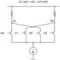
图2为线性模式ENRZ检测器的一种实施方式的示意图。输入信号w0,wl,w2,w3为承载基带码字经低通滤波处理(未图示)后的基带符号的接收线路信号,并根据ENRZ码的特定子信道与晶体管连接。也就是说,子信道向量的正值表示相应线路与对输出有正性贡献的晶体管连接,而负值表示相应线路与对输出的负性部分有贡献的晶体管连接。因此,在图2中,各线路根据子信道向量[1,-1,1,-1]与晶体管连接,而差分输出QH和QL对应于由下述计算生成的线性组合结果:Figure 2 is a schematic diagram of one embodiment of a linear mode ENRZ detector. The input signals w0, wl, w2, w3 are receiving line signals carrying baseband codewords processed by low-pass filtering (not shown), and are connected to transistors according to specific sub-channels of ENRZ codes. That is, a positive value of a subchannel vector indicates that the corresponding line is connected to a transistor that contributes positively to the output, while a negative value indicates that the corresponding line is connected to a transistor that contributes to the negative portion of the output. Thus, in Figure 2, the lines are connected to the transistors according to the subchannel vector [1, -1, 1, -1], and the differential outputs QH and QL correspond to the linear combination results generated by the following calculation:
Q=(w0+w2)-(w1+w3) (式2)Q=(w0+w2)-(w1+w3) (Formula 2)
如《Holden 1》中所述,式2具有输入信号不同排列组合形式的三个实例能够有效检测出ENRZ码的三个子信道数据输出。因此图1基带检测器130可由图2电路的三个实例构成。As described in "
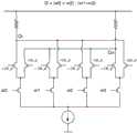
图3为实施图2中MIC的同一线性组合的同步切换解调MIC电路(本文也称“MIC解调电路”)的实施方式,其中,工作于载波频率下的解调信号CK_d用于对该MIC解调电路的操作进行选通,以实现对载波调制码字的载波调制符号的同步检测。在实际实施方式中,CK_d锁相至图1倍频器160所提供的载波频率。如图3所示,MIC解调电路获取载波调制码字的一组载波调制符号。每一个载波调制符号均可经多线路总线的多条线路中的相应线路接收,并可在施加至图示一组晶体管中的相应晶体管之前经高通(或带通)滤波处理。每一个晶体管均根据子信道向量的元素与一对输出节点中的相应输出节点连接。例如,在图3示例中,与线路[w0,w1,w2,w3]相连的一组晶体管根据子信道向量[1,-1,1,-1]与一对输出节点QL和QH连接,而子信道向量与式1给出的H4阿达玛矩阵的第二行相对应。构成其他两条子信道的MIC的各组晶体管可根据H4阿达玛矩阵中与[1,-1,1,-1]子信道向量正交的其他子信道向量与各对输出节点连接。在一些其他实施方式中,所述一组晶体管中的每一个晶体管均可根据子信道向量向载波调制符号分别施加相应的幅度权重。下式3为含有幅度各异的子信道向量的具体矩阵。幅度权重可例如根据晶体管相对尺寸、电流源幅度和/或多个并联等尺寸晶体管的数目施加。所述一组晶体管的导电性同步切换,并根据工作于从载波调制符号中恢复的频率下的解调信号CK_d控制,以响应生成解调子信道数据输出,该输出作为根据式2对所述一组载波调制符号进行的线性组合。该线性组合在所述一对输出节点上形成差分电压。Fig. 3 is the embodiment of the synchronous switch demodulation MIC circuit (also referred to as "MIC demodulation circuit" herein) implementing the same linear combination of MIC in Fig. 2, wherein, the demodulation signal CK_d working under the carrier frequency is used for Operation of the MIC demodulation circuit is gated to enable synchronous detection of carrier modulation symbols of the carrier modulation codeword. In an actual implementation, CK_d is phase-locked to the carrier frequency provided by the

图4为MIC解调ENRZ检测器的另一实施方式。该MIC解调电路以动态模式工作,以在工作于符号频率下的采样时钟CK为低电平时,对所述一对输出节点QH和QL的节点电容进行充电,并在当CK为高电平时,选择性地通过所述一组输入晶体管为所述节点提供放电至接地点的放电路径。当所述两节点放电时,输出节点QH和QL生成与式2结果对应的差分输出信号。在此类实施方式中,在对载波调制符号进行解调且根据采样时钟对线性组合进行采样时,该采样时钟同时还作为解调信号。此类实施方式可在采样时钟频率和载波频率相等时实施。在一些替代实施方式中,如图所示,可通过解调信号CK_d实现同步切换,以对检测器在载波频率下的动态操作进行周期性的中断或选通,从而实现对载波调制信号的直接检测。在一些此类实施方式中,解调信号CK_d可以为采样时钟CK基带符号波特率的整数倍,如2倍、3倍等。或者,解调信号的频率可以为采样时钟频率的一定分数。Fig. 4 is another embodiment of the MIC demodulation ENRZ detector. The MIC demodulation circuit operates in a dynamic mode to charge the node capacitances of the pair of output nodes QH and QL when the sampling clock CK operating at the symbol frequency is at a low level, and to charge the node capacitances of the pair of output nodes QH and QL when the sampling clock CK is at a high level. , selectively providing a discharge path for the node to a ground point through the set of input transistors. When the two nodes are discharged, the output nodes QH and QL generate a differential output signal corresponding to the result of
图5为图3半波同步检测器的相应全波版本。与半波检测器一致,在解调信号CK_d+及其锁相至载波频率的反信号(或称互补信号)CK_d-的作用下,对同步切换ENRZ检测进行选通。在一种替代实施方式中,每一个差分晶体管对均可由接收同一个解调信号CK_d+的NMOS器件和PMOS器件构成。在该全波电路版本中,每一个输入对所述一对输出节点的贡献均相隔半个时钟周期交替引导至反转和未反转结果输出上,从而有效地将输出信号加倍,并大大减小输出滤波需求。所述引导由与所述一对输出节点连接的多个差分晶体管对实施,以使得该组晶体管中的每一个晶体管均根据解调信号及其反信号与相应输出节点相连。如图所示,接收载波调制符号的所述一组晶体管通过相应差分晶体管对交替连接于所述一对输出节点之间。对于每一个子信道MIC,所述差分晶体管对可根据相互正交的多个子信道向量中的相应子信道向量连接。在图5中,所述差分晶体管对根据子信道向量[1,-1,1,-1]连接至所述一对输出节点。Figure 5 is the corresponding full-wave version of the half-wave synchronous detector of Figure 3 . Consistent with the half-wave detector, under the action of the demodulation signal CK_d+ and its phase-locked inverse signal (or complementary signal) CK_d- to the carrier frequency, the synchronous switching ENRZ detection is gated. In an alternative implementation manner, each differential transistor pair may be composed of an NMOS device and a PMOS device receiving the same demodulation signal CK_d+. In this version of the full-wave circuit, the contribution of each input to the pair of output nodes is alternately directed to the inverted and non-inverted resulting outputs half a clock cycle apart, effectively doubling the output signal and greatly reducing Small output filtering requirements. Said steering is implemented by a plurality of differential transistor pairs connected to said pair of output nodes such that each transistor of the set of transistors is connected to a corresponding output node according to the demodulated signal and its inverse signal. As shown, the set of transistors receiving carrier modulation symbols are alternately connected between the pair of output nodes through corresponding differential transistor pairs. For each sub-channel MIC, the differential transistor pairs may be connected according to a corresponding sub-channel vector of a plurality of mutually orthogonal sub-channel vectors. In FIG. 5, the differential transistor pair is connected to the pair of output nodes according to the sub-channel vector [1, -1, 1, -1].
图6所示为图4离散半波动态同步检测器的相应离散全波版本。采样时钟CK控制该电路的动态充放电操作,而解调信号CK_d+及其互补信号CK_d-按照上述方式对检测进行选通,以使得其与载波频率同步。Figure 6 shows the corresponding discrete full-wave version of the discrete half-wave dynamic synchronous detector of Figure 4. The sampling clock CK controls the dynamic charge and discharge operation of the circuit, while the demodulation signal CK_d+ and its complement CK_d- gate the detection as described above so that it is synchronized with the carrier frequency.
在图4和图6示例中,所述两个时钟信号的时序协调至与动态电路的操作相容。具体而言,在图4中,在每一个与时钟CK_d和CK高电平对应的放电或积分周期之前,可进行与时钟CK低电平对应的预充电操作。在图6中,时钟CK的整个周期(即预充电周期和放电周期)可与CK_d的半个周期相对应。或者,该电路的积分时间可长至足以跨越CK_d的两个或更多个半周期。在另一替代实施方式中,解调信号CK_d+/-可以为CK的整数倍。在此类实施方式中,多个CK_d周期可基本上将信号选通引入或引出积分周期。在此类实施方式中,所述一对输出节点根据采样时钟预充电,而且该对输出节点仅在当晶体管输入端的载波调制符号极性正确时才放电。在全波实施方式中,所述一对输出节点持续放电,但与此同时,由于载波调制符号根据调制内容交替变化,因此接收载波调制符号的所述一组晶体管与所述一对输出节点根据解调信号交替接断。In the FIG. 4 and FIG. 6 examples, the timing of the two clock signals is coordinated to be compatible with the operation of the dynamic circuit. Specifically, in FIG. 4 , before each discharge or integration period corresponding to clock CK_d and CK high level, a precharge operation corresponding to clock CK low level may be performed. In FIG. 6 , the entire period of the clock CK (ie, the precharge period and the discharge period) may correspond to half a period of CK_d. Alternatively, the integration time of the circuit can be long enough to span two or more half cycles of CK_d. In another alternative embodiment, the demodulated signal CK_d+/− may be an integer multiple of CK. In such implementations, multiple CK_d periods may essentially gate the signal into or out of the integration period. In such implementations, the pair of output nodes are precharged according to the sampling clock, and the pair of output nodes are only discharged when the polarity of the carrier modulation symbol at the transistor input is correct. In the full-wave implementation, the pair of output nodes is continuously discharged, but at the same time, since the carrier modulation symbol alternately changes according to the modulation content, the group of transistors receiving the carrier modulation symbol and the pair of output nodes are connected according to The demodulated signal is switched on and off alternately.
半波和全波同步检测器的操作示于图7波形。如《Hormati 3》中所述,发送器通过将发送数据与载波频率时钟相乘而生成载波调制信号。接收器本地生成载波频率解调时钟后,通过以同步检测器将该解调时钟与接收信号相结合而生成可检测的接收数据信号。载波调制信号编码成载波调制码字的载波调制符号后,经多线路总线的线路发送。The operation of half-wave and full-wave synchronous detectors is shown in Figure 7 with waveforms. As described in "
图7所示归零(RTZ)波形为半波检测器电路输出的一例,而全波波形为全波检测器电路输出的一例。在一些实施方式中,所述两种输出均经过低通滤波处理,以有助于重构所检测的波形以及消除虚假的信号伪影。随后,如图中垂直哈希标记所示,每一个波形在数据间隔中心处采样。The return-to-zero (RTZ) waveform shown in FIG. 7 is an example of the output of the half-wave detector circuit, and the full-wave waveform is an example of the output of the full-wave detector circuit. In some embodiments, both outputs are low-pass filtered to facilitate reconstruction of the detected waveform and to remove spurious signal artifacts. Each waveform is then sampled at the center of the data interval, as indicated by the vertical hash marks in the figure.
图8A为以现有多PLL方法为如图1所示等实施方式生成所需接收时钟的框图。其中,利用直接或间接从接收数据(该数据可含有经专用线路,专用子信道以及/或者经增强处理的边沿跃迁密度、眼图宽度或边沿测量结果等传输的时钟)获得的信息,生成正确定时的采样时钟,以实现所检测基带数据的最佳采样。这一方法通称为时钟数据对齐或时钟数据恢复(CDA或CDR)。在常见实施方式中,采用通过以相位检测器控制压控振荡器(VCO)来生成具有所需特性的本地时钟信号的PLL构造。FIG. 8A is a block diagram of generating required receive clocks for implementations such as those shown in FIG. 1 using an existing multi-PLL method. where, using information obtained directly or indirectly from the received data (which may contain clocks transmitted over dedicated lines, dedicated sub-channels, and/or enhanced edge transition densities, eye widths, or edge measurements, etc.), the correct Timed sample clock for optimal sampling of detected baseband data. This method is commonly known as clock data alignment or clock data recovery (CDA or CDR). In a common implementation, a PLL configuration is employed that generates a local clock signal with the desired characteristics by controlling a voltage controlled oscillator (VCO) with a phase detector.
此外,还由独立的PLL构造生成与所接收的载波解调数据的载波频率对齐的本地时钟信号以及适于对载波解调数据进行最佳采样的采样时钟。In addition, a local clock signal aligned with the carrier frequency of the received carrier demodulated data and a sampling clock adapted to optimally sample the carrier demodulated data are also generated by a separate PLL configuration.
在一种替代实施方式中,可从另一时钟信号中获得所需本地时钟信号中的一个或多个。图8B所示为以PLL生成的本地时钟信号,该PLL锁定至得自基带数据的参考信号。作为代表性示例,该操作可通过含专用时钟信号的基带数据或通过以确保的边沿跃迁密度进行增强处理的基带数据进行促进。随后,这一得到良好控制的稳定本地时钟可用于生成其他本地时钟信号,该生成既可通过众所周知的分频或倍频(如利用图1的倍频器160)方法完成,也可仅以相位插值器或可调延迟元件(如以偏移校正元件140)调节所得时钟的相对相位的方式完成。例如,得自基带数据的本地时钟信号可具有与载波频率相同的频率,并因而可通过以相位检测器和相位插值器进行相位调整而生成解调信号。此外,如果解调子信道数据的数据速率与基带数据的数据速率相等,则可以以得自基带数据的时钟驱动解调子信道数据采样时钟的生成,并可进行相应的移相操作。在载波频率与基带数据的数据速率不同的一些实施方式中,可通过对得自基带数据的采样时钟进行倍频/分频(未图示)来生成具有载波频率的解调信号(与图1所示情形一致)。随后,可通过对解调信号进行鉴相或移相操作而使其与载波调制符号对齐。图8B所示为按照这种方式获得的两个时钟,每一个时钟均分别以相应相位检测器和相位插值器进行相位调节操作。在一些实施方式中,所述相位调节的目的在于补偿基带/载波信号在经历不同滤波处理等过程时产生的信号路径差异。In an alternative embodiment, one or more of the required local clock signals may be derived from another clock signal. Figure 8B shows a local clock signal generated with a PLL locked to a reference signal derived from baseband data. As representative examples, this operation may be facilitated by baseband data with a dedicated clock signal or by baseband data enhanced with a guaranteed edge transition density. This well-controlled, stable local clock can then be used to generate other local clock signals, either by well-known methods of frequency division or multiplication (e.g., using
在一些实施方式中,也可采用混合时钟生成实施方式,该实施方式包括以辅助或从属PLL从按照上述方式生成的第一本地时钟生成第二本地时钟的实施方式。在此类系统结构中,所述辅助PLL可与主PLL具有不同的锁定特性,以允许对锁定时间、自激漂移、抖动等特性进行独立优化。In some embodiments, hybrid clock generation implementations may also be employed, including implementations in which an auxiliary or slave PLL is used to generate a second local clock from a first local clock generated as described above. In such system configurations, the auxiliary PLL may have different lock characteristics than the main PLL to allow independent optimization of lock time, self-excited drift, jitter, etc. characteristics.
图9为根据一些实施方式的方法900的流程图。如图所示,方法900包括获取902载波调制码字的一组载波调制符号,每一个载波调制符号均经多线路总线的多条线路中的相应的线路接收。所述一组载波调制符号中的每一个载波调制符号均施加904至一组晶体管中的相应的晶体管,所述一组晶体管根据多个子信道向量中的子信道向量连接至一对输出节点。在从所述一组载波调制符号中恢复906出解调信号CK_d后,通过根据该解调信号CK_d控制所述一组晶体管的导电性对所述一组载波调制符号进行线性组合,以生成908作为所述一对输出节点上的差分电压的解调子信道数据输出。FIG. 9 is a flowchart of a
在一些实施方式中,如图3和图4所示,控制所述一组晶体管的导电性包括,根据解调信号CK_d,选择性地启用电流源。在此类实施方式中,如图7所示,所述解调子信道数据输出为归零(RTZ)信号。In some implementations, as shown in FIGS. 3 and 4 , controlling the conductivity of the group of transistors includes selectively enabling a current source according to the demodulation signal CK_d. In such an embodiment, as shown in FIG. 7 , the demodulated sub-channel data output is a return-to-zero (RTZ) signal.
在一些实施方式中,所述导电性的控制包括,根据所述解调信号,将所述一组晶体管中的每一个晶体管在所述一对输出节点之间交替连接。在此类实施方式中,每一个晶体管电路均通过根据所述子信道向量连接至所述一对输出节点的一个相应差分晶体管对,在所述一对输出节点之间交替连接。在一些实施方式中,所述相应差分晶体管对接收所述解调信号以及该解调信号的互补信号,并且由相同类型的晶体管(如仅NMOS或PMOS)构成,而在其他实施方式中,所述差分晶体管对也可包括同时接收解调信号CK_d的NMOS和PMOS晶体管。这一构造示于图5和图6,其中,接收解调信号CK_d+和该解调信号互补信号CK_d-的差分对使得与载波调制符号连接的相应晶体管根据载波调制符号的极性在两个输出节点之间交替连接。In some embodiments, the controlling of the conductivity includes alternately connecting each transistor of the set of transistors between the pair of output nodes based on the demodulated signal. In such embodiments, each transistor circuit is alternately connected between said pair of output nodes by a respective differential transistor pair connected to said pair of output nodes according to said subchannel vector. In some embodiments, the respective differential transistor pairs receive the demodulated signal and the complement of the demodulated signal and are composed of transistors of the same type (e.g., only NMOS or PMOS), while in other embodiments, all The differential transistor pair may also include NMOS and PMOS transistors that simultaneously receive the demodulation signal CK_d. This configuration is shown in Figures 5 and 6, where receiving a differential pair of the demodulated signal CK_d+ and the complement of the demodulated signal CK_d- causes the corresponding transistors connected to the carrier modulation symbol to switch between the two outputs according to the polarity of the carrier modulation symbol Alternate connections between nodes.
在一些实施方式中,所述一组晶体管中每一个晶体管的导电性还由所施加的载波调制符号的符号值控制。在此类实施方式中,流过每一个晶体管的电流量与施加至每一晶体管的符号值成正比。在一种具体实施方式中,信号幅度如下:In some embodiments, the conductivity of each transistor of the set of transistors is also controlled by the sign value of the applied carrier modulation sign. In such implementations, the amount of current flowing through each transistor is proportional to the sign value applied to each transistor. In a specific implementation manner, the signal amplitude is as follows:
中心电压500mV;Center voltage 500mV;
500+180=680mV(+1)500+180=680mV(+1)
500-60=440mV(-1/3)500-60=440mV(-1/3)
500-60=440mV(-1/3)500-60=440mV(-1/3)
500-60=440mV(-1/3)500-60=440mV(-1/3)
其中,幅度“1”的符号表示与中心电压500mV偏离180mV,而幅度“1/3”的符号表示与中心电压500mV偏离60mV。Among them, the sign of amplitude "1" indicates the deviation of 180mV from the center voltage of 500mV, and the sign of amplitude "1/3" indicates the deviation of 60mV from the center voltage of 500mV.
在一些实施方式中,该方法进一步包括,响应于采样时钟,对所述一对输出节点进行预充电,其中,所述一组晶体管的导电性还根据所述采样时钟进行控制。此类实施方式即为上述“离散”或“动态”MIC解调电路。In some implementations, the method further includes precharging the pair of output nodes in response to a sampling clock, wherein the conductivity of the set of transistors is also controlled according to the sampling clock. Such implementations are the "discrete" or "dynamic" MIC demodulation circuits described above.
在一些实施方式中,所述一对输出节点上的差分电压通过使电流流过与所述一对输出节点连接的阻抗元件的方式形成。在一些实施方式中,所述阻抗元件可以为连接于电源和所述一对输出节点之间的电阻器,所述一对输出节点用于控制该电阻器的压降。流经所述电阻器的差分电流量在所述一对输出节点上形成差分电压。In some embodiments, the differential voltage on the pair of output nodes is formed by passing a current through impedance elements connected to the pair of output nodes. In some implementations, the impedance element may be a resistor connected between a power supply and the pair of output nodes, and the pair of output nodes is used to control a voltage drop of the resistor. The differential amount of current flowing through the resistors develops a differential voltage across the pair of output nodes.
在一些实施方式中,该方法还包括对所述解调子信道数据输出进行低通滤波处理。In some embodiments, the method further includes performing low-pass filtering on the demodulated sub-channel data output.
在一些实施方式中,获取所述一组载波调制符号包括,对叠加码字进行高通滤波处理,所述叠加码字含有所述载波调制码字的一组载波调制符号以及基带码字的一组基带符号。In some implementations, obtaining the group of carrier modulation symbols includes performing high-pass filtering on the superimposed codeword, the superimposed codeword containing a group of carrier modulation symbols of the carrier modulation codeword and a group of baseband codewords baseband symbol.
在一些实施方式中,所述子信道向量为构成正交矩阵各行的相互正交的多个子信道向量的一部分。在一些此类实施方式中,所述正交矩阵为阿达玛矩阵。In some embodiments, the sub-channel vector is a part of a plurality of mutually orthogonal sub-channel vectors constituting each row of the orthogonal matrix. In some such embodiments, the orthogonal matrix is a Hadamard matrix.
在一些实施方式中,所述解调信号的频率与所述数据流波特率的关联采样时钟的频率相等。在替代实施方式中,所述解调信号的频率与采样时钟频率不同。在一些此类实施方式中,所述解调信号可以为采样时钟的整数倍,并且可在单个单位间隔中启动多个放电周期。或者,所述解调信号可以为采样时钟的某一分数。在此类实施方式中,所述采样时钟可在所述解调信号的半个周期内启动多个预充电/放电周期。在一些实施方式中,所述解调信号通过以倍频器对所述采样时钟进行倍频的方式生成。或者,所述解调信号可通过以分频器对所述采样时钟进行分频的方式生成。In some embodiments, the frequency of the demodulated signal is equal to the frequency of the sampling clock associated with the baud rate of the data stream. In an alternative embodiment, the frequency of the demodulated signal is different from the sampling clock frequency. In some such implementations, the demodulated signal may be an integer multiple of a sampling clock, and multiple discharge cycles may be initiated in a single unit interval. Alternatively, the demodulated signal may be a certain fraction of the sampling clock. In such implementations, the sampling clock may initiate multiple precharge/discharge cycles within a half cycle of the demodulated signal. In some embodiments, the demodulated signal is generated by multiplying the sampling clock by a frequency multiplier. Alternatively, the demodulated signal may be generated by dividing the frequency of the sampling clock by a frequency divider.
Claims (20)
Translated fromChinesePriority Applications (2)
| Application Number | Priority Date | Filing Date | Title |
|---|---|---|---|
| CN202310631757.XACN116614338A (en) | 2017-12-28 | 2018-12-28 | Method and apparatus for synchronously switching multiple-input demodulation comparators |
| CN202310627906.5ACN116614337A (en) | 2017-12-28 | 2018-12-28 | Method and apparatus for synchronously switching multiple-input demodulation comparators |
Applications Claiming Priority (3)
| Application Number | Priority Date | Filing Date | Title |
|---|---|---|---|
| US201762611523P | 2017-12-28 | 2017-12-28 | |
| US62/611,523 | 2017-12-28 | ||
| PCT/US2018/067994WO2019133897A1 (en) | 2017-12-28 | 2018-12-28 | Synchronously-switched multi-input demodulating comparator |
Related Child Applications (2)
| Application Number | Title | Priority Date | Filing Date |
|---|---|---|---|
| CN202310631757.XADivisionCN116614338A (en) | 2017-12-28 | 2018-12-28 | Method and apparatus for synchronously switching multiple-input demodulation comparators |
| CN202310627906.5ADivisionCN116614337A (en) | 2017-12-28 | 2018-12-28 | Method and apparatus for synchronously switching multiple-input demodulation comparators |
Publications (2)
| Publication Number | Publication Date |
|---|---|
| CN111684772A CN111684772A (en) | 2020-09-18 |
| CN111684772Btrue CN111684772B (en) | 2023-06-16 |
Family
ID=65139270
Family Applications (3)
| Application Number | Title | Priority Date | Filing Date |
|---|---|---|---|
| CN202310627906.5APendingCN116614337A (en) | 2017-12-28 | 2018-12-28 | Method and apparatus for synchronously switching multiple-input demodulation comparators |
| CN202310631757.XAPendingCN116614338A (en) | 2017-12-28 | 2018-12-28 | Method and apparatus for synchronously switching multiple-input demodulation comparators |
| CN201880084127.2AActiveCN111684772B (en) | 2017-12-28 | 2018-12-28 | Synchronous switching multiple-input demodulation comparator |
Family Applications Before (2)
| Application Number | Title | Priority Date | Filing Date |
|---|---|---|---|
| CN202310627906.5APendingCN116614337A (en) | 2017-12-28 | 2018-12-28 | Method and apparatus for synchronously switching multiple-input demodulation comparators |
| CN202310631757.XAPendingCN116614338A (en) | 2017-12-28 | 2018-12-28 | Method and apparatus for synchronously switching multiple-input demodulation comparators |
Country Status (5)
| Country | Link |
|---|---|
| US (4) | US10693688B2 (en) |
| EP (1) | EP3732840B1 (en) |
| KR (3) | KR102452390B1 (en) |
| CN (3) | CN116614337A (en) |
| WO (1) | WO2019133897A1 (en) |
Families Citing this family (7)
| Publication number | Priority date | Publication date | Assignee | Title |
|---|---|---|---|---|
| US10693587B2 (en) | 2017-07-10 | 2020-06-23 | Kandou Labs, S.A. | Multi-wire permuted forward error correction |
| US11128129B2 (en)* | 2019-04-08 | 2021-09-21 | Kandou Labs, S.A. | Distributed electrostatic discharge scheme to improve analog front-end bandwidth of receiver in high-speed signaling system |
| CN114079605B (en)* | 2020-08-13 | 2023-05-23 | 立锜科技股份有限公司 | Communication signal demodulation device and communication signal demodulation method |
| US11831472B1 (en) | 2022-08-30 | 2023-11-28 | Kandou Labs SA | Pre-scaler for orthogonal differential vector signalling |
| WO2024124047A2 (en) | 2022-12-09 | 2024-06-13 | Kandou Labs SA | Mapping non-return-to-zero to ensemble non-return-to-zero signaling |
| US20240283549A1 (en)* | 2023-02-17 | 2024-08-22 | Tektronix, Inc. | Methods and systems of phase aligning a replica carrier signal for use in demodulating a subcarrier signal |
| CN119254589B (en)* | 2024-12-03 | 2025-03-28 | 深圳市意创兴业科技有限公司 | Low-voltage communication demodulation platform |
Citations (5)
| Publication number | Priority date | Publication date | Assignee | Title |
|---|---|---|---|---|
| CN103166888A (en)* | 2011-12-16 | 2013-06-19 | 恩德莱斯和豪瑟尔测量及调节技术分析仪表两合公司 | Electronic circuit and method for recovering desired signal from carrier signal by demodulation and modem |
| US9077386B1 (en)* | 2010-05-20 | 2015-07-07 | Kandou Labs, S.A. | Methods and systems for selection of unions of vector signaling codes for power and pin efficient chip-to-chip communication |
| WO2015131203A1 (en)* | 2014-02-28 | 2015-09-03 | Kandou Lab, S.A. | Clock-embedded vector signaling codes |
| CN106576087A (en)* | 2014-08-01 | 2017-04-19 | 康杜实验室公司 | Orthogonal Differential Vector Signaling Codes with Embedded Clocks |
| CN106664272A (en)* | 2014-07-21 | 2017-05-10 | 康杜实验室公司 | multipoint data transmission |
Family Cites Families (229)
| Publication number | Priority date | Publication date | Assignee | Title |
|---|---|---|---|---|
| US3196351A (en) | 1962-06-26 | 1965-07-20 | Bell Telephone Labor Inc | Permutation code signaling |
| US3970795A (en) | 1974-07-16 | 1976-07-20 | The Post Office | Measurement of noise in a communication channel |
| JPS5279747A (en) | 1975-12-26 | 1977-07-05 | Sony Corp | Noise removal circuit |
| US4206316A (en) | 1976-05-24 | 1980-06-03 | Hughes Aircraft Company | Transmitter-receiver system utilizing pulse position modulation and pulse compression |
| US4181967A (en) | 1978-07-18 | 1980-01-01 | Motorola, Inc. | Digital apparatus approximating multiplication of analog signal by sine wave signal and method |
| US4414512A (en) | 1981-05-29 | 1983-11-08 | Motorola Inc. | Broadband peak detector |
| US4499550A (en) | 1982-09-30 | 1985-02-12 | General Electric Company | Walsh function mixer and tone detector |
| US5053974A (en) | 1987-03-31 | 1991-10-01 | Texas Instruments Incorporated | Closeness code and method |
| US7606575B2 (en) | 1988-08-04 | 2009-10-20 | Broadcom Corporation | Remote radio data communication system with data rate switching |
| US5168509A (en) | 1989-04-12 | 1992-12-01 | Kabushiki Kaisha Toshiba | Quadrature amplitude modulation communication system with transparent error correction |
| US5166956A (en) | 1990-05-21 | 1992-11-24 | North American Philips Corporation | Data transmission system and apparatus providing multi-level differential signal transmission |
| US5150384A (en) | 1990-09-28 | 1992-09-22 | Motorola, Inc. | Carrier recovery method and apparatus having an adjustable response time determined by carrier signal parameters |
| EP0543070A1 (en) | 1991-11-21 | 1993-05-26 | International Business Machines Corporation | Coding system and method using quaternary codes |
| US5311516A (en) | 1992-05-29 | 1994-05-10 | Motorola, Inc. | Paging system using message fragmentation to redistribute traffic |
| US5388126A (en) | 1992-12-21 | 1995-02-07 | Rypinski; Chandos A. | Baseband signal processor for a microwave radio receiver |
| US5412689A (en) | 1992-12-23 | 1995-05-02 | International Business Machines Corporation | Modal propagation of information through a defined transmission medium |
| KR950012709B1 (en)* | 1992-12-31 | 1995-10-20 | 현대전자산업주식회사 | Depletion transistor type delay circuit |
| US5449895A (en) | 1993-12-22 | 1995-09-12 | Xerox Corporation | Explicit synchronization for self-clocking glyph codes |
| US5553097A (en) | 1994-06-01 | 1996-09-03 | International Business Machines Corporation | System and method for transporting high-bandwidth signals over electrically conducting transmission lines |
| US5659353A (en) | 1995-03-17 | 1997-08-19 | Bell Atlantic Network Services, Inc. | Television distribution system and method |
| US6658234B1 (en)* | 1995-06-02 | 2003-12-02 | Northrop Grumman Corporation | Method for extending the effective dynamic range of a radio receiver system |
| US5856935A (en) | 1996-05-08 | 1999-01-05 | Motorola, Inc. | Fast hadamard transform within a code division, multiple access communication system |
| US5727006A (en) | 1996-08-15 | 1998-03-10 | Seeo Technology, Incorporated | Apparatus and method for detecting and correcting reverse polarity, in a packet-based data communications system |
| US5982954A (en) | 1996-10-21 | 1999-11-09 | University Technology Corporation | Optical field propagation between tilted or offset planes |
| US6005895A (en) | 1996-12-20 | 1999-12-21 | Rambus Inc. | Apparatus and method for multilevel signaling |
| US6084883A (en) | 1997-07-07 | 2000-07-04 | 3Com Corporation | Efficient data transmission over digital telephone networks using multiple modulus conversion |
| US6111895A (en) | 1997-05-14 | 2000-08-29 | At&T Corp. | Wideband transmission through wire |
| US6154498A (en) | 1997-09-26 | 2000-11-28 | Intel Corporation | Computer system with a semi-differential bus signaling scheme |
| US6480548B1 (en) | 1997-11-17 | 2002-11-12 | Silicon Graphics, Inc. | Spacial derivative bus encoder and decoder |
| US6292559B1 (en) | 1997-12-19 | 2001-09-18 | Rice University | Spectral optimization and joint signaling techniques with upstream/downstream separation for communication in the presence of crosstalk |
| US6317465B1 (en) | 1998-02-10 | 2001-11-13 | Matsushita Electric Industrial Co., Ltd. | Data transmission system |
| US6686879B2 (en) | 1998-02-12 | 2004-02-03 | Genghiscomm, Llc | Method and apparatus for transmitting and receiving signals having a carrier interferometry architecture |
| EP0966133B1 (en) | 1998-06-15 | 2005-03-02 | Sony International (Europe) GmbH | Orthogonal transformations for interference reduction in multicarrier systems |
| US6522699B1 (en) | 1998-06-19 | 2003-02-18 | Nortel Networks Limited | Transmission system for reduction of amateur radio interference |
| US6084958A (en) | 1998-06-23 | 2000-07-04 | Starium Ltd | Determining the manner in which the wires connecting to a base set of a telephone system are used for transmission and reception of electrical signals representing a communication |
| US6226330B1 (en) | 1998-07-16 | 2001-05-01 | Silicon Graphics, Inc. | Eigen-mode encoding of signals in a data group |
| US6097732A (en) | 1998-10-30 | 2000-08-01 | Advanced Micro Devices, Inc. | Apparatus and method for controlling transmission parameters of selected home network stations transmitting on a telephone medium |
| US6278740B1 (en) | 1998-11-19 | 2001-08-21 | Gates Technology | Multi-bit (2i+2)-wire differential coding of digital signals using differential comparators and majority logic |
| US6650699B1 (en)* | 1999-01-21 | 2003-11-18 | International Business Machines Corporation | Methods and apparatus for timing recovery from a sampled and equalized data signal |
| US6483828B1 (en) | 1999-02-10 | 2002-11-19 | Ericsson, Inc. | System and method for coding in a telecommunications environment using orthogonal and near-orthogonal codes |
| US6556628B1 (en) | 1999-04-29 | 2003-04-29 | The University Of North Carolina At Chapel Hill | Methods and systems for transmitting and receiving differential signals over a plurality of conductors |
| US6697420B1 (en) | 1999-05-25 | 2004-02-24 | Intel Corporation | Symbol-based signaling for an electromagnetically-coupled bus system |
| US7120198B1 (en) | 1999-05-26 | 2006-10-10 | The Aerospace Corporation | Quadrature product subcarrier modulation system |
| US6535560B1 (en)* | 1999-06-03 | 2003-03-18 | Ditrans Corporation | Coherent adaptive calibration system and method |
| US7269212B1 (en) | 2000-09-05 | 2007-09-11 | Rambus Inc. | Low-latency equalization in multi-level, multi-line communication systems |
| US7555263B1 (en) | 1999-10-21 | 2009-06-30 | Broadcom Corporation | Adaptive radio transceiver |
| US7072387B1 (en) | 1999-12-15 | 2006-07-04 | Paradyne Corporation | Fractional bit rate encoding in a discrete multi-tone communication system |
| WO2001045279A1 (en)* | 1999-12-17 | 2001-06-21 | Nokia Corporation | Linearisation method and signal processing device |
| US6650638B1 (en) | 2000-03-06 | 2003-11-18 | Agilent Technologies, Inc. | Decoding method and decoder for 64b/66b coded packetized serial data |
| US6954492B1 (en) | 2000-04-19 | 2005-10-11 | 3Com Corporation | Method of differential encoding a precoded multiple modulus encoder |
| US6865236B1 (en) | 2000-06-01 | 2005-03-08 | Nokia Corporation | Apparatus, and associated method, for coding and decoding multi-dimensional biorthogonal codes |
| JP2002016531A (en) | 2000-06-27 | 2002-01-18 | Nec Corp | Cdma communication system and its method |
| US20020044316A1 (en) | 2000-10-16 | 2002-04-18 | Myers Michael H. | Signal power allocation apparatus and method |
| EP1202483A1 (en) | 2000-10-27 | 2002-05-02 | Alcatel | Correlated spreading sequences for high rate non-coherent communication systems |
| EP1204228B1 (en) | 2000-11-06 | 2005-05-18 | Alcatel | Optical modulation scheme for NRZ signals and optical transmitter |
| US6807234B2 (en) | 2000-12-19 | 2004-10-19 | Intel Corporation | Method and apparatus for constellation mapping and bitloading in multi-carrier transceivers, such as DMT-based DSL transceivers |
| US6661355B2 (en) | 2000-12-27 | 2003-12-09 | Apple Computer, Inc. | Methods and apparatus for constant-weight encoding & decoding |
| US6766342B2 (en) | 2001-02-15 | 2004-07-20 | Sun Microsystems, Inc. | System and method for computing and unordered Hadamard transform |
| WO2002071770A1 (en) | 2001-03-06 | 2002-09-12 | Beamreach Networks, Inc. | Adaptive communications methods for multiple user packet radio wireless networks |
| US20020152340A1 (en) | 2001-03-29 | 2002-10-17 | International Business Machines Corporation | Pseudo-differential parallel source synchronous bus |
| US8498368B1 (en) | 2001-04-11 | 2013-07-30 | Qualcomm Incorporated | Method and system for optimizing gain changes by identifying modulation type and rate |
| TW569534B (en) | 2001-05-15 | 2004-01-01 | Via Tech Inc | Data transmission system using differential signals as edge alignment triggering signals and input/output buffers thereof |
| WO2002095955A1 (en) | 2001-05-22 | 2002-11-28 | Koninklijke Philips Electronics N.V. | Method of decoding a variable-length codeword sequence |
| US6452420B1 (en) | 2001-05-24 | 2002-09-17 | National Semiconductor Corporation | Multi-dimensional differential signaling (MDDS) |
| US7298785B2 (en)* | 2001-07-04 | 2007-11-20 | Kabushiki Kaisha Toyota Chuo Kenkyusho | Multicarrier demodulation method and apparatus, and multicarrier modulation method and apparatus |
| US7236757B2 (en) | 2001-07-11 | 2007-06-26 | Vativ Technologies, Inc. | High-speed multi-channel communications transceiver with inter-channel interference filter |
| US6621427B2 (en) | 2001-10-11 | 2003-09-16 | Sun Microsystems, Inc. | Method and apparatus for implementing a doubly balanced code |
| US6999516B1 (en) | 2001-10-24 | 2006-02-14 | Rambus Inc. | Technique for emulating differential signaling |
| US7142612B2 (en) | 2001-11-16 | 2006-11-28 | Rambus, Inc. | Method and apparatus for multi-level signaling |
| US7039136B2 (en) | 2001-11-19 | 2006-05-02 | Tensorcomm, Inc. | Interference cancellation in a signal |
| JP2003163612A (en) | 2001-11-26 | 2003-06-06 | Advanced Telecommunication Research Institute International | Digital signal encoding method and decoding method |
| US6993311B2 (en) | 2002-02-20 | 2006-01-31 | Freescale Semiconductor, Inc. | Radio receiver having an adaptive equalizer and method therefor |
| US7134056B2 (en) | 2002-06-04 | 2006-11-07 | Lucent Technologies Inc. | High-speed chip-to-chip communication interface with signal trace routing and phase offset detection |
| AU2003249708A1 (en) | 2002-07-03 | 2004-01-23 | Hughes Electronics Corporation | Method and system for memory management in low density parity check (ldpc) decoders |
| US7787572B2 (en) | 2005-04-07 | 2010-08-31 | Rambus Inc. | Advanced signal processors for interference cancellation in baseband receivers |
| US7127003B2 (en) | 2002-09-23 | 2006-10-24 | Rambus Inc. | Method and apparatus for communicating information using different signaling types |
| EP1404029B1 (en) | 2002-09-24 | 2007-12-12 | Agilent Technologies, Inc. | Method and apparatus for predicting a signalling code corresponding to a code spur |
| US7586972B2 (en) | 2002-11-18 | 2009-09-08 | The Aerospace Corporation | Code division multiple access enhanced capacity system |
| US7236535B2 (en) | 2002-11-19 | 2007-06-26 | Qualcomm Incorporated | Reduced complexity channel estimation for wireless communication systems |
| US7023817B2 (en) | 2003-03-11 | 2006-04-04 | Motorola, Inc. | Method and apparatus for source device synchronization in a communication system |
| JP4492920B2 (en) | 2003-05-27 | 2010-06-30 | ルネサスエレクトロニクス株式会社 | Differential signal transmission system |
| US6876317B2 (en) | 2003-05-30 | 2005-04-05 | Texas Instruments Incorporated | Method of context based adaptive binary arithmetic decoding with two part symbol decoding |
| WO2004112247A1 (en)* | 2003-06-16 | 2004-12-23 | Nec Corporation | Logic circuit having suppressed leak current to differential circuit |
| US7358869B1 (en) | 2003-08-20 | 2008-04-15 | University Of Pittsburgh | Power efficient, high bandwidth communication using multi-signal-differential channels |
| US7428273B2 (en) | 2003-09-18 | 2008-09-23 | Promptu Systems Corporation | Method and apparatus for efficient preamble detection in digital data receivers |
| KR100976489B1 (en) | 2003-10-01 | 2010-08-18 | 엘지전자 주식회사 | Control method of data modulation and coding method applied to multi-input multi-output system of mobile communication |
| US7639596B2 (en) | 2003-12-07 | 2009-12-29 | Adaptive Spectrum And Signal Alignment, Inc. | High speed multiple loop DSL system |
| WO2005062509A1 (en) | 2003-12-18 | 2005-07-07 | National Institute Of Information And Communications Technology | Transmitter, receiver, transmitting method, receiving method, and program |
| US20050213686A1 (en) | 2004-03-26 | 2005-09-29 | Texas Instruments Incorporated | Reduced complexity transmit spatial waterpouring technique for multiple-input, multiple-output communication systems |
| KR100629675B1 (en) | 2004-07-16 | 2006-09-28 | 학교법인 포항공과대학교 | Current mode differential transmission method and system of three data using four signal lines |
| US7599390B2 (en) | 2004-07-21 | 2009-10-06 | Rambus Inc. | Approximate bit-loading for data transmission over frequency-selective channels |
| EP1774655A1 (en) | 2004-07-27 | 2007-04-18 | Koninklijke Philips Electronics N.V. | Encoding of data words using three or more signal levels |
| US7460612B2 (en) | 2004-08-12 | 2008-12-02 | Texas Instruments Incorporated | Method and apparatus for a fully digital quadrature modulator |
| KR101151130B1 (en) | 2004-08-17 | 2012-06-04 | 삼성전자주식회사 | Method and apparatus for transmitting and receiving data using full rate full diversity stbc |
| US7869546B2 (en) | 2004-09-30 | 2011-01-11 | Telefonaktiebolaget Lm Ericsson (Publ) | Multicode transmission using Walsh Hadamard transform |
| US7746764B2 (en) | 2004-10-22 | 2010-06-29 | Parkervision, Inc. | Orthogonal signal generation using vector spreading and combining |
| US7327803B2 (en) | 2004-10-22 | 2008-02-05 | Parkervision, Inc. | Systems and methods for vector power amplification |
| ITVA20040054A1 (en) | 2004-11-23 | 2005-02-23 | St Microelectronics Srl | METHOD FOR ESTIMATING CANE ATTENUATION COEFFICIENTS, METHOD OF RECEIVING SYMBOLS AND RELATIVE RECEIVER AND TRANSMITTER TO SINGLE ANTENNA OR MULTI-ANTENNA |
| US7496162B2 (en) | 2004-11-30 | 2009-02-24 | Stmicroelectronics, Inc. | Communication system with statistical control of gain |
| US20060126751A1 (en) | 2004-12-10 | 2006-06-15 | Anthony Bessios | Technique for disparity bounding coding in a multi-level signaling system |
| US7349484B2 (en)* | 2004-12-22 | 2008-03-25 | Rambus Inc. | Adjustable dual-band link |
| KR100947792B1 (en) | 2005-03-08 | 2010-03-15 | 퀄컴 인코포레이티드 | Transmission method and apparatus for combining pulse position modulation and hierarchical modulation |
| US20060251421A1 (en) | 2005-05-09 | 2006-11-09 | Ben Gurion University Of The Negev, Research And Development Authority | Improved free space optical bus |
| US7656321B2 (en) | 2005-06-02 | 2010-02-02 | Rambus Inc. | Signaling system |
| US7529323B2 (en) | 2005-06-06 | 2009-05-05 | The Aerospace Corporation | Quaternary precoded continuous phase modulation soft bit metric demodulator |
| EP1909424A1 (en) | 2005-07-27 | 2008-04-09 | Naoki Suehiro | Data communication system and data transmitting apparatus |
| US7808883B2 (en) | 2005-08-08 | 2010-10-05 | Nokia Corporation | Multicarrier modulation with enhanced frequency coding |
| KR100906125B1 (en) | 2005-09-26 | 2009-07-07 | 삼성전자주식회사 | Apparatus and method for detecting fast feedback information in broadband wireless communication system |
| US7356213B1 (en) | 2006-03-28 | 2008-04-08 | Sun Microsystems, Inc. | Transparent switch using optical and electrical proximity communication |
| JP3919803B1 (en) | 2006-04-17 | 2007-05-30 | 株式会社アドバンテスト | Characteristic acquisition apparatus, method and program |
| KR100744141B1 (en) | 2006-07-21 | 2007-08-01 | 삼성전자주식회사 | Virtual differential interconnect circuit and virtual differential signaling scheme for single-ended signal lines |
| US8295250B2 (en) | 2006-07-24 | 2012-10-23 | Qualcomm Incorporated | Code interleaving for a structured code |
| KR101249359B1 (en) | 2006-08-18 | 2013-04-01 | 삼성전자주식회사 | Method and apparatus for transmitting/receiving channel quality information in an orthogonal frequency division multiplexing system supporting a multi-input multi-output |
| US20080104374A1 (en) | 2006-10-31 | 2008-05-01 | Motorola, Inc. | Hardware sorter |
| US8023570B2 (en) | 2007-02-06 | 2011-09-20 | Massachusetts Institute Of Technology | System and apparatus for error control codes based on layering and linear transformations |
| CN101286775A (en) | 2007-04-12 | 2008-10-15 | 北京三星通信技术研究有限公司 | Multi-antenna spatial multiplexing system using enhanced signal detection |
| US8199841B1 (en) | 2007-04-26 | 2012-06-12 | Marvell International Ltd. | Channel tracking in a wireless multiple-input multiple-output (MIMO) communication system |
| KR100871711B1 (en) | 2007-05-03 | 2008-12-08 | 삼성전자주식회사 | Multiphase Transmit / Receive Circuits Supporting Single-Ended Signaling and Differential Signaling and Clocking Methods for Single-Ended Signaling Transition in Differential Signaling |
| US8102934B2 (en) | 2007-08-16 | 2012-01-24 | Samsung Electronics Co., Ltd. | Transmitting apparatus and method |
| US20090059782A1 (en) | 2007-08-29 | 2009-03-05 | Rgb Systems, Inc. | Method and apparatus for extending the transmission capability of twisted pair communication systems |
| CN101399798B (en) | 2007-09-27 | 2011-07-06 | 北京信威通信技术股份有限公司 | Steady signal transmission method and device for OFDMA radio communication system |
| EP2208327A4 (en) | 2007-10-01 | 2012-01-04 | Rambus Inc | Simplified receiver for use in multi-wire communication |
| US9197470B2 (en) | 2007-10-05 | 2015-11-24 | Innurvation, Inc. | Data transmission via multi-path channels using orthogonal multi-frequency signals with differential phase shift keying modulation |
| WO2009058790A1 (en) | 2007-10-30 | 2009-05-07 | Rambus Inc. | Signaling with superimposed differential-mode and common-mode signals |
| US7899653B2 (en) | 2007-10-30 | 2011-03-01 | Micron Technology, Inc. | Matrix modeling of parallel data structures to facilitate data encoding and/or jittery signal generation |
| WO2009067633A1 (en) | 2007-11-20 | 2009-05-28 | California Institute Of Technology | Rank modulation for memory devices |
| JP2009134573A (en) | 2007-11-30 | 2009-06-18 | Nec Corp | Multi-chip semiconductor device and data transfer method |
| WO2009075936A1 (en) | 2007-12-07 | 2009-06-18 | Rambus Inc. | Encoding and decoding techniques for bandwidth-efficient communication |
| EP2071786B1 (en) | 2007-12-14 | 2020-12-23 | Vodafone Holding GmbH | Method and transceiver for data communication |
| US8588254B2 (en) | 2007-12-17 | 2013-11-19 | Broadcom Corporation | Method and system for energy efficient signaling for 100mbps Ethernet using a subset technique |
| KR100934007B1 (en) | 2007-12-18 | 2009-12-28 | 한국전자통신연구원 | Apparatus and method for multi-dimensional detection in multi-input multi-output receiver, and receiving device using same |
| US20090163162A1 (en) | 2007-12-19 | 2009-06-25 | Hoffman Stephen W | Direct conversion receiving architecture with an integrated tuner self alignment function |
| US8588280B2 (en) | 2007-12-19 | 2013-11-19 | Rambus Inc. | Asymmetric communication on shared links |
| CN101601199B (en) | 2007-12-28 | 2013-04-17 | 日本电气株式会社 | Signal processing and method for multi-sector wireless communication system |
| US8055095B2 (en) | 2008-01-23 | 2011-11-08 | Sparsense, Inc. | Parallel and adaptive signal processing |
| FR2927205A1 (en) | 2008-01-31 | 2009-08-07 | Commissariat Energie Atomique | LOW PAPR SPATIO-TEMPORAL ENCODING METHOD FOR IMPULSE UWB TYPE MULTI-ANTENNA COMMUNICATION SYSTEM |
| KR100963410B1 (en) | 2008-03-11 | 2010-06-14 | 한국전자통신연구원 | Cooperative Receive Diversity Apparatus and Method Based on Signal Point Rearrangement or Superposition Modulation in Relay System |
| US8644497B2 (en) | 2008-04-24 | 2014-02-04 | Lantiq Deutschland Gmbh | Method and apparatus for adding a communication connection to a vectored group |
| CN101610115A (en) | 2008-06-20 | 2009-12-23 | 华为技术有限公司 | Optical signal generation method and device |
| US20160204823A1 (en)* | 2008-08-07 | 2016-07-14 | Trex Enterprises Corporation | 10GbE E-band radio with 8PSK modulation |
| JP5266325B2 (en) | 2008-08-18 | 2013-08-21 | 日本電信電話株式会社 | Vector synthesis type phase shifter, optical transceiver and control circuit |
| US20100046644A1 (en) | 2008-08-19 | 2010-02-25 | Motorola, Inc. | Superposition coding |
| JP2010062944A (en) | 2008-09-04 | 2010-03-18 | Kyushu Institute Of Technology | Wireless communications system, wireless reception device, and wireless transmission device |
| FR2936384A1 (en) | 2008-09-22 | 2010-03-26 | St Microelectronics Grenoble | DEVICE FOR EXCHANGING DATA BETWEEN COMPONENTS OF AN INTEGRATED CIRCUIT |
| US8103287B2 (en) | 2008-09-30 | 2012-01-24 | Apple Inc. | Methods and apparatus for resolving wireless signal components |
| KR101173942B1 (en) | 2008-11-28 | 2012-08-14 | 한국전자통신연구원 | Data transmission device, data receiving device, data transmitting system and method for transmitting data |
| WO2010065789A2 (en) | 2008-12-03 | 2010-06-10 | Rambus Inc. | Resonance mitigation for high-speed signaling |
| CN101714961B (en)* | 2009-01-05 | 2012-09-05 | 南京师范大学 | Digital signal transmitting method and equipment based on modulated carriers of equal amplitude and equal period |
| US8472513B2 (en) | 2009-01-14 | 2013-06-25 | Lsi Corporation | TX back channel adaptation algorithm |
| JP4748227B2 (en) | 2009-02-10 | 2011-08-17 | ソニー株式会社 | Data modulation apparatus and method |
| TWI430622B (en) | 2009-02-23 | 2014-03-11 | Inst Information Industry | Signal transmission apparatus, transmission method and computer program product thereof |
| US8428177B2 (en) | 2009-02-25 | 2013-04-23 | Samsung Electronics Co., Ltd. | Method and apparatus for multiple input multiple output (MIMO) transmit beamforming |
| CN101854223A (en) | 2009-03-31 | 2010-10-06 | 上海交通大学 | Vector Quantization Codebook Generation Method |
| ES2452569T3 (en)* | 2009-04-08 | 2014-04-02 | Fraunhofer-Gesellschaft zur Förderung der angewandten Forschung e.V. | Device, procedure and computer program for mixing upstream audio signal with downstream mixing using phase value smoothing |
| JP2010283735A (en)* | 2009-06-08 | 2010-12-16 | Seiko Epson Corp | Detection device and solid-state imaging device |
| JP5187277B2 (en) | 2009-06-16 | 2013-04-24 | ソニー株式会社 | Information processing apparatus and mode switching method |
| WO2011009584A2 (en) | 2009-07-20 | 2011-01-27 | Lantiq Deutschland Gmbh | Method and apparatus for vectored data communication |
| EP2456515A4 (en) | 2009-07-20 | 2013-01-23 | Nat Ict Australia Ltd | NEURO-STIMULATION |
| KR101079603B1 (en) | 2009-08-11 | 2011-11-03 | 주식회사 티엘아이 | Differential Data Transmitting and Receiving Device and Method with using 3 level volatge |
| KR20120095408A (en) | 2009-10-30 | 2012-08-28 | 뱅거 유니버시티 | Synchronisation process in optical frequency division multiplexing transmission systems |
| US8767640B2 (en) | 2009-11-09 | 2014-07-01 | Adeptence, Llc | Method and apparatus for directional centralized contention based period in a wireless communication system |
| US8279745B2 (en) | 2009-11-23 | 2012-10-02 | Telefonaktiebolaget L M Ericsson (Publ) | Orthogonal vector DSL |
| JP2011118998A (en) | 2009-12-04 | 2011-06-16 | Elpida Memory Inc | Semiconductor device |
| TW201145918A (en) | 2009-12-27 | 2011-12-16 | Maxlinear Inc | Methods and apparatus for synchronization in multiple-channel communication systems |
| TWI562554B (en) | 2009-12-30 | 2016-12-11 | Sony Corp | Communications system and device using beamforming |
| CN102014475B (en) | 2010-01-08 | 2012-01-04 | 华为技术有限公司 | Resource mapping and code division multiplexing method and device |
| US8457261B1 (en) | 2010-02-17 | 2013-06-04 | Qualcomm Incorporated | Automatic gain control techniques for detecting RF saturation |
| US9288089B2 (en) | 2010-04-30 | 2016-03-15 | Ecole Polytechnique Federale De Lausanne (Epfl) | Orthogonal differential vector signaling |
| US9246713B2 (en) | 2010-05-20 | 2016-01-26 | Kandou Labs, S.A. | Vector signaling with reduced receiver complexity |
| US8539318B2 (en) | 2010-06-04 | 2013-09-17 | École Polytechnique Fédérale De Lausanne (Epfl) | Power and pin efficient chip-to-chip communications with common-mode rejection and SSO resilience |
| US9401828B2 (en) | 2010-05-20 | 2016-07-26 | Kandou Labs, S.A. | Methods and systems for low-power and pin-efficient communications with superposition signaling codes |
| US8649445B2 (en) | 2011-02-17 | 2014-02-11 | École Polytechnique Fédérale De Lausanne (Epfl) | Methods and systems for noise resilient, pin-efficient and low power communications with sparse signaling codes |
| US9596109B2 (en) | 2010-05-20 | 2017-03-14 | Kandou Labs, S.A. | Methods and systems for high bandwidth communications interface |
| US8718184B1 (en) | 2012-05-03 | 2014-05-06 | Kandou Labs S.A. | Finite state encoders and decoders for vector signaling codes |
| US8755426B1 (en) | 2012-03-15 | 2014-06-17 | Kandou Labs, S.A. | Rank-order equalization |
| US8385387B2 (en) | 2010-05-20 | 2013-02-26 | Harris Corporation | Time dependent equalization of frequency domain spread orthogonal frequency division multiplexing using decision feedback equalization |
| US8989317B1 (en) | 2010-05-20 | 2015-03-24 | Kandou Labs, S.A. | Crossbar switch decoder for vector signaling codes |
| US9300503B1 (en)* | 2010-05-20 | 2016-03-29 | Kandou Labs, S.A. | Methods and systems for skew tolerance in and advanced detectors for vector signaling codes for chip-to-chip communication |
| US9479369B1 (en) | 2010-05-20 | 2016-10-25 | Kandou Labs, S.A. | Vector signaling codes with high pin-efficiency for chip-to-chip communication and storage |
| US9071476B2 (en) | 2010-05-20 | 2015-06-30 | Kandou Labs, S.A. | Methods and systems for high bandwidth chip-to-chip communications interface |
| US9288082B1 (en)* | 2010-05-20 | 2016-03-15 | Kandou Labs, S.A. | Circuits for efficient detection of vector signaling codes for chip-to-chip communication using sums of differences |
| US8880783B2 (en) | 2011-07-05 | 2014-11-04 | Kandou Labs SA | Differential vector storage for non-volatile memory |
| US9124557B2 (en) | 2010-05-20 | 2015-09-01 | Kandou Labs, S.A. | Methods and systems for chip-to-chip communication with reduced simultaneous switching noise |
| US9251873B1 (en) | 2010-05-20 | 2016-02-02 | Kandou Labs, S.A. | Methods and systems for pin-efficient memory controller interface using vector signaling codes for chip-to-chip communications |
| US8593305B1 (en) | 2011-07-05 | 2013-11-26 | Kandou Labs, S.A. | Efficient processing and detection of balanced codes |
| WO2011151469A1 (en) | 2010-06-04 | 2011-12-08 | Ecole Polytechnique Federale De Lausanne | Error control coding for orthogonal differential vector signaling |
| US9331962B2 (en) | 2010-06-27 | 2016-05-03 | Valens Semiconductor Ltd. | Methods and systems for time sensitive networks |
| US8773964B2 (en) | 2010-09-09 | 2014-07-08 | The Regents Of The University Of California | CDMA-based crosstalk cancellation for on-chip global high-speed links |
| KR20120050620A (en)* | 2010-11-11 | 2012-05-21 | 삼성전자주식회사 | Device for receiving dual band signal using multi-band antenna in wireless receiver |
| US8750176B2 (en) | 2010-12-22 | 2014-06-10 | Apple Inc. | Methods and apparatus for the intelligent association of control symbols |
| US8620166B2 (en) | 2011-01-07 | 2013-12-31 | Raytheon Bbn Technologies Corp. | Holevo capacity achieving joint detection receiver |
| US8949693B2 (en) | 2011-03-04 | 2015-02-03 | Hewlett-Packard Development Company, L.P. | Antipodal-mapping-based encoders and decoders |
| US8644330B2 (en)* | 2011-03-29 | 2014-02-04 | Intel Corporation | Architecture and method of channel estimation for wireless communication system |
| US8238318B1 (en) | 2011-08-17 | 2012-08-07 | CBF Networks, Inc. | Intelligent backhaul radio |
| FR2985125A1 (en) | 2011-12-21 | 2013-06-28 | France Telecom | METHOD FOR TRANSMITTING A DIGITAL SIGNAL FOR A SEMI-ORTHOGONAL MS-MARC SYSTEM, PROGRAM PRODUCT, AND CORRESPONDING RELAY DEVICE |
| KR102276433B1 (en) | 2012-02-07 | 2021-07-12 | 마벨 월드 트레이드 리미티드 | Pilot sequence design for long range wlan |
| US9537644B2 (en) | 2012-02-23 | 2017-01-03 | Lattice Semiconductor Corporation | Transmitting multiple differential signals over a reduced number of physical channels |
| US8711919B2 (en) | 2012-03-29 | 2014-04-29 | Rajendra Kumar | Systems and methods for adaptive blind mode equalization |
| US8996740B2 (en) | 2012-06-29 | 2015-03-31 | Qualcomm Incorporated | N-phase polarity output pin mode multiplexer |
| US9191256B2 (en) | 2012-12-03 | 2015-11-17 | Digital PowerRadio, LLC | Systems and methods for advanced iterative decoding and channel estimation of concatenated coding systems |
| WO2014124450A1 (en) | 2013-02-11 | 2014-08-14 | Kandou Labs, S.A. | Methods and systems for high bandwidth chip-to-chip communications interface |
| CN103516650B (en) | 2013-09-10 | 2016-06-01 | 华中科技大学 | The incoherent unitary space-time modulation of a kind of mimo wireless communication to sole of the foot demodulation method and to sole of the foot detuner |
| US9100232B1 (en) | 2014-02-02 | 2015-08-04 | Kandou Labs, S.A. | Method for code evaluation using ISI ratio |
| US9270390B2 (en) | 2014-03-28 | 2016-02-23 | Olympus Corporation | Frequency and phase offset compensation of modulated signals with symbol timing recovery |
| US9509437B2 (en) | 2014-05-13 | 2016-11-29 | Kandou Labs, S.A. | Vector signaling code with improved noise margin |
| US9710412B2 (en) | 2014-05-15 | 2017-07-18 | Qualcomm Incorporated | N-factorial voltage mode driver |
| US9148087B1 (en)* | 2014-05-16 | 2015-09-29 | Kandou Labs, S.A. | Symmetric is linear equalization circuit with increased gain |
| JP6699911B2 (en) | 2014-06-11 | 2020-05-27 | マーベル ワールド トレード リミテッド | Compressed preamble for wireless communication system |
| US9852806B2 (en) | 2014-06-20 | 2017-12-26 | Kandou Labs, S.A. | System for generating a test pattern to detect and isolate stuck faults for an interface using transition coding |
| GB2527604A (en) | 2014-06-27 | 2015-12-30 | Ibm | Data encoding in solid-state storage devices |
| US9432082B2 (en) | 2014-07-17 | 2016-08-30 | Kandou Labs, S.A. | Bus reversable orthogonal differential vector signaling codes |
| US9674014B2 (en) | 2014-10-22 | 2017-06-06 | Kandou Labs, S.A. | Method and apparatus for high speed chip-to-chip communications |
| US9942884B2 (en) | 2015-05-15 | 2018-04-10 | Nokia Technologies Oy | Efficient uplink data indication techniques for MIMO-OFDMA transmission in WLAN |
| US9998154B2 (en)* | 2015-06-22 | 2018-06-12 | Qualcomm Incorporated | Low power physical layer driver topologies |
| KR101978470B1 (en)* | 2015-06-26 | 2019-05-14 | 칸도우 랩스 에스에이 | High-speed communication system |
| US10055372B2 (en) | 2015-11-25 | 2018-08-21 | Kandou Labs, S.A. | Orthogonal differential vector signaling codes with embedded clock |
| US10070385B2 (en)* | 2015-12-31 | 2018-09-04 | Texas Instruments Incorporated | Multi-band concurrent multi-channel receiver |
| JP6700854B2 (en)* | 2016-02-26 | 2020-05-27 | ラピスセミコンダクタ株式会社 | Semiconductor device |
| US9853615B2 (en)* | 2016-04-13 | 2017-12-26 | Avago Technologies General Ip (Singapore) Pte. Ltd. | Linearized dynamic amplifier |
| US9941916B2 (en) | 2016-06-03 | 2018-04-10 | Texas Instruments Incorporated | Multi-band programmable receiver |
| US10116468B1 (en) | 2017-06-28 | 2018-10-30 | Kandou Labs, S.A. | Low power chip-to-chip bidirectional communications |
| US20190103903A1 (en) | 2017-10-02 | 2019-04-04 | Mediatek Inc. | Codebook Designs To Support ULA And Non-ULA Scenarios |
| US10347283B2 (en) | 2017-11-02 | 2019-07-09 | Kandou Labs, S.A. | Clock data recovery in multilane data receiver |
| US10243614B1 (en)* | 2018-01-26 | 2019-03-26 | Kandou Labs, S.A. | Method and system for calibrating multi-wire skew |
| WO2019148139A1 (en) | 2018-01-26 | 2019-08-01 | California Institute Of Technology | Systems and methods for communicating by modulating data on zeros |
| US10873345B2 (en) | 2018-02-05 | 2020-12-22 | Qualcomm Incorporated | Enhanced polar code construction |
| KR102707165B1 (en) | 2018-06-12 | 2024-09-13 | 칸도우 랩스 에스에이 | Passive multi-input comparator for orthogonal codes on multi-wire buses |
| US11424777B2 (en) | 2018-06-14 | 2022-08-23 | Ubiqam Ltd. | Methods and systems for mitigation of interference signals for a wireless network receiver |
| US11128129B2 (en) | 2019-04-08 | 2021-09-21 | Kandou Labs, S.A. | Distributed electrostatic discharge scheme to improve analog front-end bandwidth of receiver in high-speed signaling system |
- 2018
- 2018-12-28EPEP18837129.8Apatent/EP3732840B1/enactiveActive
- 2018-12-28WOPCT/US2018/067994patent/WO2019133897A1/ennot_activeCeased
- 2018-12-28USUS16/236,012patent/US10693688B2/enactiveActive
- 2018-12-28KRKR1020217042541Apatent/KR102452390B1/enactiveActive
- 2018-12-28KRKR1020207020492Apatent/KR102347396B1/enactiveActive
- 2018-12-28CNCN202310627906.5Apatent/CN116614337A/enactivePending
- 2018-12-28CNCN202310631757.XApatent/CN116614338A/enactivePending
- 2018-12-28KRKR1020227034446Apatent/KR102498475B1/enactiveActive
- 2018-12-28CNCN201880084127.2Apatent/CN111684772B/enactiveActive
- 2020
- 2020-06-23USUS16/909,529patent/US11063799B2/enactiveActive
- 2021
- 2021-07-04USUS17/367,392patent/US11469931B2/enactiveActive
- 2022
- 2022-10-11USUS18/045,713patent/US11894961B2/enactiveActive
Patent Citations (5)
| Publication number | Priority date | Publication date | Assignee | Title |
|---|---|---|---|---|
| US9077386B1 (en)* | 2010-05-20 | 2015-07-07 | Kandou Labs, S.A. | Methods and systems for selection of unions of vector signaling codes for power and pin efficient chip-to-chip communication |
| CN103166888A (en)* | 2011-12-16 | 2013-06-19 | 恩德莱斯和豪瑟尔测量及调节技术分析仪表两合公司 | Electronic circuit and method for recovering desired signal from carrier signal by demodulation and modem |
| WO2015131203A1 (en)* | 2014-02-28 | 2015-09-03 | Kandou Lab, S.A. | Clock-embedded vector signaling codes |
| CN106664272A (en)* | 2014-07-21 | 2017-05-10 | 康杜实验室公司 | multipoint data transmission |
| CN106576087A (en)* | 2014-08-01 | 2017-04-19 | 康杜实验室公司 | Orthogonal Differential Vector Signaling Codes with Embedded Clocks |
Non-Patent Citations (1)
| Title |
|---|
| 基于KQ-100K的电力线载波通信系统的优化设计;杨瑞等;《电子元器件应用》;20081215(第12期);全文* |
Also Published As
| Publication number | Publication date |
|---|---|
| US20230062846A1 (en) | 2023-03-02 |
| US11894961B2 (en) | 2024-02-06 |
| US11063799B2 (en) | 2021-07-13 |
| KR20220140029A (en) | 2022-10-17 |
| EP3732840B1 (en) | 2024-05-01 |
| CN111684772A (en) | 2020-09-18 |
| CN116614337A (en) | 2023-08-18 |
| WO2019133897A1 (en) | 2019-07-04 |
| KR20200100708A (en) | 2020-08-26 |
| US11469931B2 (en) | 2022-10-11 |
| US20190207793A1 (en) | 2019-07-04 |
| EP3732840A1 (en) | 2020-11-04 |
| KR20220000944A (en) | 2022-01-04 |
| KR102498475B1 (en) | 2023-02-09 |
| KR102347396B1 (en) | 2022-01-04 |
| US20210336824A1 (en) | 2021-10-28 |
| CN116614338A (en) | 2023-08-18 |
| KR102452390B1 (en) | 2022-10-06 |
| US10693688B2 (en) | 2020-06-23 |
| US20200322194A1 (en) | 2020-10-08 |
Similar Documents
| Publication | Publication Date | Title |
|---|---|---|
| CN111684772B (en) | Synchronous switching multiple-input demodulation comparator | |
| US11863358B2 (en) | High speed communications system |
Legal Events
| Date | Code | Title | Description |
|---|---|---|---|
| PB01 | Publication | ||
| PB01 | Publication | ||
| SE01 | Entry into force of request for substantive examination | ||
| SE01 | Entry into force of request for substantive examination | ||
| GR01 | Patent grant | ||
| GR01 | Patent grant |