CN111665403B - Method, device and system for locating failure points of laminated electronic components - Google Patents
Method, device and system for locating failure points of laminated electronic componentsDownload PDFInfo
- Publication number
- CN111665403B CN111665403BCN202010355856.6ACN202010355856ACN111665403BCN 111665403 BCN111665403 BCN 111665403BCN 202010355856 ACN202010355856 ACN 202010355856ACN 111665403 BCN111665403 BCN 111665403B
- Authority
- CN
- China
- Prior art keywords
- electronic component
- laminated electronic
- infrared image
- infrared
- laminated
- Prior art date
- Legal status (The legal status is an assumption and is not a legal conclusion. Google has not performed a legal analysis and makes no representation as to the accuracy of the status listed.)
- Active
Links
- 238000000034methodMethods0.000titleclaimsabstractdescription38
- 230000002159abnormal effectEffects0.000claimsabstractdescription60
- 238000004458analytical methodMethods0.000claimsabstractdescription41
- 238000001931thermographyMethods0.000claimsabstractdescription40
- 239000000523sampleSubstances0.000claimsdescription34
- 238000001514detection methodMethods0.000claimsdescription19
- 238000012545processingMethods0.000claimsdescription16
- 238000012876topographyMethods0.000claimsdescription15
- 239000003985ceramic capacitorSubstances0.000claimsdescription11
- 238000010586diagramMethods0.000claimsdescription11
- 239000000919ceramicSubstances0.000claimsdescription9
- 238000004590computer programMethods0.000claimsdescription9
- 230000003287optical effectEffects0.000claimsdescription8
- 238000004891communicationMethods0.000claimsdescription5
- 238000012360testing methodMethods0.000abstractdescription12
- 238000010438heat treatmentMethods0.000abstractdescription4
- 239000003990capacitorSubstances0.000description24
- 238000005516engineering processMethods0.000description9
- 230000007246mechanismEffects0.000description4
- 230000008569processEffects0.000description4
- 238000012512characterization methodMethods0.000description3
- 238000012790confirmationMethods0.000description3
- 230000006872improvementEffects0.000description2
- 238000009413insulationMethods0.000description2
- 230000009467reductionEffects0.000description2
- 230000005856abnormalityEffects0.000description1
- 230000009286beneficial effectEffects0.000description1
- 230000005540biological transmissionEffects0.000description1
- 238000006243chemical reactionMethods0.000description1
- 230000001066destructive effectEffects0.000description1
- 238000011161developmentMethods0.000description1
- 238000010191image analysisMethods0.000description1
- 238000012986modificationMethods0.000description1
- 230000004048modificationEffects0.000description1
- 238000009659non-destructive testingMethods0.000description1
- 238000002360preparation methodMethods0.000description1
- 230000005855radiationEffects0.000description1
- 230000003068static effectEffects0.000description1
- 239000010409thin filmSubstances0.000description1
Images


Classifications
- G—PHYSICS
- G01—MEASURING; TESTING
- G01R—MEASURING ELECTRIC VARIABLES; MEASURING MAGNETIC VARIABLES
- G01R31/00—Arrangements for testing electric properties; Arrangements for locating electric faults; Arrangements for electrical testing characterised by what is being tested not provided for elsewhere
- G01R31/003—Environmental or reliability tests
- G—PHYSICS
- G01—MEASURING; TESTING
- G01J—MEASUREMENT OF INTENSITY, VELOCITY, SPECTRAL CONTENT, POLARISATION, PHASE OR PULSE CHARACTERISTICS OF INFRARED, VISIBLE OR ULTRAVIOLET LIGHT; COLORIMETRY; RADIATION PYROMETRY
- G01J5/00—Radiation pyrometry, e.g. infrared or optical thermometry
- G01J5/0096—Radiation pyrometry, e.g. infrared or optical thermometry for measuring wires, electrical contacts or electronic systems
- G—PHYSICS
- G01—MEASURING; TESTING
- G01J—MEASUREMENT OF INTENSITY, VELOCITY, SPECTRAL CONTENT, POLARISATION, PHASE OR PULSE CHARACTERISTICS OF INFRARED, VISIBLE OR ULTRAVIOLET LIGHT; COLORIMETRY; RADIATION PYROMETRY
- G01J5/00—Radiation pyrometry, e.g. infrared or optical thermometry
- G01J5/48—Thermography; Techniques using wholly visual means
- G01J5/485—Temperature profile
- G—PHYSICS
- G01—MEASURING; TESTING
- G01J—MEASUREMENT OF INTENSITY, VELOCITY, SPECTRAL CONTENT, POLARISATION, PHASE OR PULSE CHARACTERISTICS OF INFRARED, VISIBLE OR ULTRAVIOLET LIGHT; COLORIMETRY; RADIATION PYROMETRY
- G01J5/00—Radiation pyrometry, e.g. infrared or optical thermometry
- G01J2005/0077—Imaging
Landscapes
- Physics & Mathematics (AREA)
- General Physics & Mathematics (AREA)
- Spectroscopy & Molecular Physics (AREA)
- Engineering & Computer Science (AREA)
- Environmental & Geological Engineering (AREA)
- Investigating Or Analyzing Materials Using Thermal Means (AREA)
Abstract
Translated fromChinese
Description
Translated fromChinese技术领域technical field
本申请涉及层叠型电子元件检测技术领域,特别是涉及一种层叠型电子元件的失效点定位方法、装置和系统。The present application relates to the technical field of detection of stacked electronic components, in particular to a method, device and system for locating failure points of stacked electronic components.
背景技术Background technique
伴随着电子产品不断向小、轻、薄的方向发展,与之匹配的电子元件也不断向叠层化发展,如多层片式陶瓷电容、多层片式压敏电阻等。层叠型电子元件主要由介质体、内层电极和端电极组成。With the continuous development of electronic products in the direction of small, light and thin, the matching electronic components are also continuously developing in stacking, such as multilayer chip ceramic capacitors, multilayer chip varistors, etc. Laminated electronic components are mainly composed of dielectric bodies, inner electrodes and terminal electrodes.
近年来,人们对产品可靠性的要求越来越高,对多层片式陶瓷电容、多层片式压敏电阻等层叠型电子元件提出了更高的要求。绝缘电阻降低或短路失效是层叠型电子元件的主要失效模式,对电子产品的可靠性构成极大威胁。为了提高层叠型电子元件的可靠性,需要针对其开展失效分析,明晰其失效机理,方能提出改进建议。In recent years, people's requirements for product reliability have become higher and higher, and higher requirements have been put forward for laminated electronic components such as multilayer chip ceramic capacitors and multilayer chip varistors. Insulation resistance reduction or short-circuit failure is the main failure mode of laminated electronic components, which poses a great threat to the reliability of electronic products. In order to improve the reliability of laminated electronic components, it is necessary to carry out failure analysis and clarify its failure mechanism before putting forward suggestions for improvement.
在实现过程中,发明人发现传统技术中至少存在如下问题:对于层叠型电子元件,其失效点的定位较为困难。当前的主要分析方法为将失效样品固封,制成切片进行观察。由于机械研磨制作切片方法得到的剖面是不连续的,如果失效样品的失效点小于研磨的步长,则有可能造成失效点的定位失败,导致失效样品失效机理的无法确定。During the implementation process, the inventors found at least the following problems in the traditional technology: for the stacked electronic components, it is difficult to locate the failure point. The current main analysis method is to immobilize the failed samples and make slices for observation. Since the cross-section obtained by mechanical grinding is discontinuous, if the failure point of the failed sample is smaller than the grinding step, it may cause the failure to locate the failure point, resulting in the uncertainty of the failure mechanism of the failed sample.
发明内容Contents of the invention
基于此,有必要针对传统技术对层叠型电子元件的失效点定位存在准确度低的问题,提供一种层叠型电子元件的失效点定位方法、装置和系统。Based on this, it is necessary to provide a method, device and system for locating failure points of stacked electronic components in view of the problem of low accuracy of failure point location of stacked electronic components in traditional technologies.
为了实现上述目的,一方面,本申请实施例提供了一种层叠型电子元件的失效点定位方法,包括:In order to achieve the above purpose, on the one hand, an embodiment of the present application provides a method for locating failure points of laminated electronic components, including:
获取层叠型电子元件的第一红外图像;层叠型电子元件为施加电信号的失效电子元件;第一红外图像为对层叠型电子元件的介质体的第一表面进行红外热成像分析得到的温度分布图;Acquiring the first infrared image of the stacked electronic component; the stacked electronic component is a failed electronic component that applies an electrical signal; the first infrared image is the temperature distribution obtained by infrared thermal imaging analysis on the first surface of the dielectric body of the stacked electronic component picture;
获取层叠型电子元件的第二红外图像;第二红外图像为对层叠型电子元件的介质体的第二表面进行红外热成像分析得到的温度分布图;第一表面与第二表面呈夹角设置;Obtaining a second infrared image of the laminated electronic component; the second infrared image is a temperature distribution map obtained by infrared thermal imaging analysis of the second surface of the dielectric body of the laminated electronic component; the first surface and the second surface are set at an angle ;
根据第一红外图像和第二红外图像,得到层叠型电子元件的异常热点的三维坐标。According to the first infrared image and the second infrared image, the three-dimensional coordinates of the abnormal hot spot of the laminated electronic component are obtained.
在其中一个实施例中,根据第一红外图像和第二红外图像,得到层叠型电子元件的异常热点的三维坐标的步骤包括:In one of the embodiments, according to the first infrared image and the second infrared image, the step of obtaining the three-dimensional coordinates of the abnormal hot spot of the laminated electronic component includes:
从第一红外图像中获取异常热点的第一位置坐标;Obtaining the first position coordinates of the abnormal hot spot from the first infrared image;
从第二红外图像中获取异常热点的第二位置坐标;Obtaining second position coordinates of the abnormal hot spot from the second infrared image;
根据第一位置坐标和第二位置坐标,得到三维坐标。According to the first position coordinates and the second position coordinates, three-dimensional coordinates are obtained.
在其中一个实施例中,根据第一红外图像和第二红外图像,得到层叠型电子元件的异常热点的三维坐标的步骤之后,还包括:In one of the embodiments, after the step of obtaining the three-dimensional coordinates of the abnormal hot spot of the laminated electronic component according to the first infrared image and the second infrared image, it further includes:
根据三维坐标获取异常热点的形貌图;形貌图为根据三维坐标对层叠型电子元件进行切片及检测得到。The topography map of the abnormal hot spot is obtained according to the three-dimensional coordinates; the topography map is obtained by slicing and detecting the stacked electronic components according to the three-dimensional coordinates.
在其中一个实施例中,获取层叠型电子元件的第一红外图像的步骤之前,还包括:In one of the embodiments, before the step of acquiring the first infrared image of the laminated electronic component, it also includes:
对层叠型电子元件施加电信号;电信号为矩形波。An electrical signal is applied to a laminated electronic component; the electrical signal is a rectangular wave.
在其中一个实施例中,矩形波的周期的取值范围为100毫秒至500毫秒;In one of the embodiments, the period of the rectangular wave ranges from 100 milliseconds to 500 milliseconds;
矩形波的峰值的取值范围为0.1伏至5伏。The peak value of the rectangular wave ranges from 0.1 volts to 5 volts.
在其中一个实施例中,失效电子元件为多层陶瓷电容器或叠层型压敏电阻器;介质体为陶瓷体。In one embodiment, the failed electronic component is a multilayer ceramic capacitor or a multilayer varistor; the dielectric body is a ceramic body.
另一方面,本申请实施例还提供了一种层叠型电子元件的失效点定位装置,包括:On the other hand, the embodiment of the present application also provides a failure point location device for laminated electronic components, including:
第一红外图像获取模块,用于获取层叠型电子元件的第一红外图像;层叠型电子元件为施加电信号的失效电子元件;第一红外图像为对层叠型电子元件的介质体的第一表面进行红外热成像分析得到的温度分布图;The first infrared image acquisition module is used to acquire the first infrared image of the stacked electronic component; the stacked electronic component is a failed electronic component that applies an electrical signal; the first infrared image is the first surface of the dielectric body of the stacked electronic component The temperature distribution map obtained by infrared thermal imaging analysis;
第二红外图像获取模块,用于获取层叠型电子元件的第二红外图像;第二红外图像为对层叠型电子元件的介质体的第二表面进行红外热成像分析得到的温度分布图;第一表面与第二表面呈夹角设置;The second infrared image acquisition module is used to acquire a second infrared image of the laminated electronic component; the second infrared image is a temperature distribution map obtained by infrared thermal imaging analysis on the second surface of the dielectric body of the laminated electronic component; the first The surface and the second surface are arranged at an included angle;
三维坐标确认模块,用于根据第一红外图像和第二红外图像,得到层叠型电子元件的异常热点的三维坐标。The three-dimensional coordinate confirmation module is used to obtain the three-dimensional coordinates of the abnormal hot spot of the laminated electronic component according to the first infrared image and the second infrared image.
在其中一个实施例中,提供了一种系统,包括:In one of the embodiments, a system is provided, comprising:
样品台,用于放置层叠型电子元件;Sample stage for placing stacked electronic components;
电源,用于为层叠型电子元件施加电信号;a power supply for applying electrical signals to the stacked electronic components;
红外热成像仪探测系统,用于对层叠型电子元件进行红外热成像分析;Infrared thermal imager detection system, used for infrared thermal imaging analysis of laminated electronic components;
处理设备,与红外热成像仪探测系统通信连接;处理设备用于实现如上述的层叠型电子元件的失效点定位方法。The processing device is communicatively connected with the detection system of the infrared thermal imager; the processing device is used to realize the method for locating failure points of the above-mentioned laminated electronic components.
在其中一个实施例中,红外热成像仪探测系统包括:In one of the embodiments, the infrared thermal imager detection system includes:
光学模块;optical module;
红外热像仪探头,用于通过光学模块获取层叠型电子元件的图像信息;An infrared thermal imager probe is used to obtain image information of laminated electronic components through an optical module;
处理器,分别与红外热像仪探头和处理设备通信连接;The processor is respectively connected to the thermal imaging camera probe and the processing device in communication;
显示器,与处理器电连接。The display is electrically connected with the processor.
在其中一个实施例中,提供了一种计算机存储介质,其上存储有计算机程序,该程序被处理器执行时实现如上述的层叠型电子元件的失效点定位方法。In one embodiment, a computer storage medium is provided, on which a computer program is stored, and when the program is executed by a processor, the method for locating a failure point of a stacked electronic component as described above is implemented.
上述技术方案中的一个技术方案具有如下优点和有益效果:One of the above technical solutions has the following advantages and beneficial effects:
为失效的层叠型电子元件施加电信号,并通过红外热成像分析采集介质体的第一表面的红外图像,且采集介质体的第二表面的红外图像;其中,第一表面与第二表面是呈夹角连接的两个表面;进一步地,可根据两个表面的红外图像来确认异常热点的三维坐标,实现失效点的定位。基于此,通过相连接的两个表面的温度分布定位,能够有效提高层叠型电子元件的失效点定位的准确度,同时,不需要加热台辅助,节省失效分析时间且降低试验难度。Apply an electrical signal to the failed laminated electronic component, and collect an infrared image of the first surface of the dielectric body through infrared thermal imaging analysis, and collect an infrared image of the second surface of the dielectric body; wherein, the first surface and the second surface are Two surfaces connected at an angle; further, the three-dimensional coordinates of abnormal hot spots can be confirmed according to the infrared images of the two surfaces, and the location of the failure point can be realized. Based on this, the positioning of the temperature distribution of the two connected surfaces can effectively improve the accuracy of the failure point positioning of the laminated electronic component, and at the same time, it does not require the assistance of a heating table, which saves time for failure analysis and reduces the difficulty of testing.
附图说明Description of drawings
为了更清楚地说明本申请实施例或传统技术中的技术方案,下面将对实施例或传统技术描述中所需要使用的附图作简单地介绍,显而易见地,下面描述中的附图仅仅是本申请的一些实施例,对于本领域普通技术人员来讲,在不付出创造性劳动的前提下,还可以根据这些附图获得其他的附图。In order to more clearly illustrate the technical solutions in the embodiments of the present application or the conventional technology, the following will briefly introduce the accompanying drawings that need to be used in the description of the embodiments or the traditional technology. Obviously, the accompanying drawings in the following description are only the present invention For some embodiments of the application, those skilled in the art can also obtain other drawings based on these drawings without creative work.
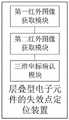
图1为一个实施例中层叠型电子元件的失效点定位方法的第一示意性流程图;Fig. 1 is the first schematic flowchart of the method for locating failure points of laminated electronic components in one embodiment;
图2为一个实施例中层叠型电子元件的结构示意图;Fig. 2 is a structural schematic diagram of a laminated electronic component in an embodiment;
图3为一个实施例中层叠型电子元件的失效点定位方法的第二示意性流程图;3 is a second schematic flow chart of a method for locating failure points of laminated electronic components in an embodiment;
图4为一个实施例中层叠型电子元件的失效点定位方法的第三示意性流程图;FIG. 4 is a third schematic flow chart of a method for locating failure points of laminated electronic components in an embodiment;
图5为一个实施例中失效多层陶瓷电容器的典型模型图;Figure 5 is a typical model diagram of a failed multilayer ceramic capacitor in one embodiment;
图6为一个实施例中失效电容的第一次红外热成像分析的结果示意图;Fig. 6 is a schematic diagram of the results of the first infrared thermal imaging analysis of the failed capacitor in one embodiment;
图7为一个实施例中失效电容的第二次红外热成像分析的结果示意图;Fig. 7 is a schematic diagram of the results of the second infrared thermal imaging analysis of the failed capacitor in one embodiment;
图8为一个实施例中失效电容的失效点的形貌示意图;其中,(a)为第一比例形貌图,(b)为第二比例形貌图,(c)为第三比例形貌图,(d)为第四比例形貌图;Fig. 8 is a schematic diagram of the appearance of the failure point of the failure capacitor in one embodiment; wherein, (a) is the first scale topography, (b) is the second scale topography, and (c) is the third scale topography Figure, (d) is the fourth scale topography;
图9为一个实施例中层叠型电子元件的失效点定位装置的示意图;9 is a schematic diagram of a failure point location device for laminated electronic components in an embodiment;
图10为一个实施例中系统的结构示意图。Fig. 10 is a schematic structural diagram of a system in an embodiment.
具体实施方式detailed description
为了便于理解本申请,下面将参照相关附图对本申请进行更全面的描述。附图中给出了本申请的实施例。但是,本申请可以以许多不同的形式来实现,并不限于本文所描述的实施例。相反地,提供这些实施例的目的是使本申请的公开内容更加透彻全面。In order to facilitate the understanding of the present application, the present application will be described more fully below with reference to the relevant drawings. Embodiments of the application are given in the drawings. However, the present application can be embodied in many different forms and is not limited to the embodiments described herein. On the contrary, the purpose of providing these embodiments is to make the disclosure of this application more thorough and comprehensive.
除非另有定义,本文所使用的所有的技术和科学术语与属于本申请的技术领域的技术人员通常理解的含义相同。本文中在本申请的说明书中所使用的术语只是为了描述具体的实施例的目的,不是旨在于限制本申请。Unless otherwise defined, all technical and scientific terms used herein have the same meaning as commonly understood by one of ordinary skill in the technical field to which this application belongs. The terms used herein in the specification of the application are only for the purpose of describing specific embodiments, and are not intended to limit the application.
可以理解,本申请所使用的术语“第一”、“第二”等可在本文中用于描述各种部件,但这些部件不受这些术语限制。这些术语仅用于将第一个部件与另一个部件区分。It can be understood that the terms "first", "second", etc. used in this application may be used to describe various components herein, but these components are not limited by these terms. These terms are only used to distinguish one component from another.
空间关系术语例如“呈夹角设置”等,在这里可以用于描述图中所示的一个元件或特征与其它元件或特征的关系。Spatially relative terms, such as "angled", etc., may be used herein to describe the relationship of one element or feature to other elements or features shown in the figures.
需要说明的是,当一个元件被认为是“连接”另一个元件时,它可以是直接连接到另一个元件,或者通过居中元件连接另一个元件。此外,以下实施例中的“连接”,如果被连接的对象之间具有电信号或数据的传递,则应理解为“电连接”、“通信连接”等。It should be noted that when an element is considered to be "connected" to another element, it may be directly connected to the other element, or connected to the other element through an intervening element. In addition, "connection" in the following embodiments should be understood as "electrical connection", "communication connection" and the like if there is transmission of electrical signals or data between the connected objects.
在此使用时,单数形式的“一”、“一个”和“所述/该”也可以包括复数形式,除非上下文清楚指出另外的方式。还应当理解的是,术语“包括/包含”或“具有”等指定所陈述的特征、整体、步骤、操作、组件、部分或它们的组合的存在,但是不排除存在或添加一个或更多个其他特征、整体、步骤、操作、组件、部分或它们的组合的可能性。同时,在本说明书中使用的术语“和/或”包括相关所列项目的任何及所有组合。When used herein, the singular forms "a", "an" and "the/the" may also include the plural forms unless the context clearly dictates otherwise. It should also be understood that the terms "comprising/comprising" or "having" etc. specify the presence of stated features, integers, steps, operations, components, parts or combinations thereof, but do not exclude the presence or addition of one or more The possibility of other features, integers, steps, operations, components, parts or combinations thereof. Meanwhile, the term "and/or" used in this specification includes any and all combinations of the related listed items.
现有的失效点定位技术包括:Existing failure point location techniques include:
(1)机械研磨与显微观察相结合的失效分析方法,例如,陶瓷电容制成金相切片样品,在研磨过程中结合参数测试以及显微观察,以此来定位失效电容的失效点,该方法较为普遍,但对于相关技术人员的要求较高,主要取决于人员的工作经验及切片手艺,同时还有一定的随机性,当失效样品的失效点较小时,容易导致失效点的定位失败。并且,该方法需要慢工细磨,花费时间较长。(1) A failure analysis method combining mechanical grinding and microscopic observation. For example, a ceramic capacitor is made into a metallographic section sample, and the parameter test and microscopic observation are combined during the grinding process to locate the failure point of the failed capacitor. The method is relatively common, but it requires high requirements for relevant technical personnel, mainly depends on the personnel's work experience and slicing skills, and also has a certain degree of randomness. When the failure point of the failed sample is small, it is easy to cause failure in the location of the failure point. Moreover, this method requires slow work and careful grinding, which takes a long time.
(2)红外热像探测结合样品台控温以及显微镜技术,从二维平面角度对电容器失效点进行定位。其定位的准确度有待进一步提高;同时,该方法是通过在失效电容器两端施加恒定电压对异常热点进行定位,随着加电时间的延长,一方面由于热斑扩大,引起定位精确度的降低,另一方面会对失效样品的异常点造成二次损失,有可能引入新的失效机理,导致失效原因的误判。此外,该方法法还需要对样品台进行控温,试验过程中需要等待加热台温度的稳定,延长了试验时间,同时试验过程中需要对样品均匀加热,对样品的要求较高,增加了试验难度。(2) Infrared thermal image detection combines the temperature control of the sample stage and microscope technology to locate the failure point of the capacitor from the perspective of a two-dimensional plane. The accuracy of its positioning needs to be further improved; at the same time, this method locates the abnormal hot spot by applying a constant voltage across the failed capacitor. As the power-on time prolongs, on the one hand, the hot spot expands, causing the positioning accuracy to decrease. , on the other hand, it will cause secondary loss to the abnormal point of the failed sample, which may introduce a new failure mechanism and lead to misjudgment of the cause of failure. In addition, this method also needs to control the temperature of the sample table. During the test, it is necessary to wait for the temperature of the heating table to stabilize, which prolongs the test time. At the same time, the sample needs to be heated evenly during the test, which has high requirements for the sample and increases the test time. difficulty.
基于以上原因,本申请实施例提供了一种基于红外热成像技术的层叠型电子元件失效定位方法,主要包括步骤:样品准备;第一次红外热成像分析(正面);第二次红外热成像分析(侧面);失效点三维定位。Based on the above reasons, the embodiment of the present application provides a failure location method for laminated electronic components based on infrared thermal imaging technology, which mainly includes steps: sample preparation; first infrared thermal imaging analysis (front); second infrared thermal imaging Analysis (side); 3D location of failure point.
在一个实施例中,提供了一种层叠型电子元件的失效点定位方法,如图1所示,包括:In one embodiment, a method for locating failure points of laminated electronic components is provided, as shown in FIG. 1 , including:
步骤S110,获取层叠型电子元件的第一红外图像;层叠型电子元件为施加电信号的失效电子元件;第一红外图像为对层叠型电子元件的介质体的第一表面进行红外热成像分析得到的温度分布图;Step S110, acquiring a first infrared image of the stacked electronic component; the stacked electronic component is a failed electronic component applied with an electrical signal; the first infrared image is obtained by performing infrared thermal imaging analysis on the first surface of the dielectric body of the stacked electronic component The temperature distribution map;
步骤S120,获取层叠型电子元件的第二红外图像;第二红外图像为对层叠型电子元件的介质体的第二表面进行红外热成像分析得到的温度分布图;第一表面与第二表面呈夹角设置;Step S120, acquiring a second infrared image of the laminated electronic component; the second infrared image is a temperature distribution map obtained by infrared thermal imaging analysis on the second surface of the dielectric body of the laminated electronic component; the first surface and the second surface are Angle setting;
步骤S130,根据第一红外图像和第二红外图像,得到层叠型电子元件的异常热点的三维坐标。Step S130, according to the first infrared image and the second infrared image, obtain the three-dimensional coordinates of the abnormal hot spot of the laminated electronic component.
具体而言,针对失效的层叠型电子元件样品,可先通过两端的电极对层叠型电子元件施加电信号。进一步地,可对施加电信号的层叠型电子元件进行红外热成像分析,获取层叠型电子元件的介质体的第一表面的温度分布图,即第一红外图像,还获取层叠型电子元件的介质体的第二表面的温度分布图,即第二红外图像;其中,第一表面与第二表面呈夹角设置,即属于两个相交的侧面,比如一个为介质体的顶面,另一个为介质体的侧面。基于介质体上两个相交的表面的红外图像,可确认层叠型电子元件的异常热点的三维坐标。基于此,通过介质体上两个相交的表面的红外图像获取三维坐标,能够快速定位到失效点的位置,可避免通电时间延长造成的热斑扩大,进而引起定位精确度降低,以及对异常热点造成二次损失的问题。基于本申请实施例,能够增加定位的准确性、节省失效分析时间且降低试验难度。Specifically, for a failed stacked electronic component sample, an electrical signal can be applied to the stacked electronic component through the electrodes at both ends. Further, the infrared thermal imaging analysis can be carried out on the laminated electronic component to which the electric signal is applied, and the temperature distribution map of the first surface of the dielectric body of the laminated electronic component is obtained, that is, the first infrared image, and the medium temperature of the laminated electronic component is also obtained. The temperature distribution map of the second surface of the body, that is, the second infrared image; wherein, the first surface and the second surface are set at an angle, that is, they belong to two intersecting sides, for example, one is the top surface of the medium body, and the other is the side of the medium. Based on the infrared images of two intersecting surfaces on the dielectric body, the three-dimensional coordinates of abnormal hot spots of the stacked electronic component can be confirmed. Based on this, the three-dimensional coordinates obtained by infrared images of two intersecting surfaces on the dielectric body can quickly locate the location of the failure point, which can avoid the expansion of the hot spot caused by the extension of the power-on time, which will cause the reduction of positioning accuracy, and the abnormal hot spot The problem of causing secondary losses. Based on the embodiment of the present application, the positioning accuracy can be increased, the failure analysis time can be saved, and the test difficulty can be reduced.
需要说明的是,本申请实施例可通过检测设备或检测系统来执行,还可通过检测人员操纵相关的检测设备来实现,此处不做具体限定。层叠型电子元件例如多层片式陶瓷电容、多层片式压敏电阻等,此处不做具体限定。层叠型电子元件的结构可如图2所示,介质体相对的两端分别设有端电极,介质体内设有内层电极;其中,介质体可为陶瓷体或有机薄膜体等,此处不做具体限定。对层叠型电子元件施加的电信号可为方波信号、恒压信号、正弦波信号或锯齿波信号等,此处不做具体限定。It should be noted that the embodiment of the present application can be implemented by a detection device or a detection system, and can also be realized by a detection personnel manipulating a related detection device, which is not specifically limited here. Stacked electronic components such as multilayer chip ceramic capacitors, multilayer chip varistors, etc. are not specifically limited here. The structure of the laminated electronic component can be shown in Figure 2, the opposite ends of the dielectric body are respectively provided with terminal electrodes, and the dielectric body is provided with inner layer electrodes; wherein, the dielectric body can be a ceramic body or an organic thin film body, etc. Be specific. The electrical signal applied to the stacked electronic component may be a square wave signal, a constant voltage signal, a sine wave signal or a sawtooth wave signal, etc., which are not specifically limited here.
层叠型电子元件的介质体为多面体,其中两个表面用于与端电极电连接,还有两个相交的表面可用于红外热成像分析,实现快速确认异常热点的三维坐标;示例性地,第一表面与第二表面的夹角可为80°、85°、90°或100°等,此处不做具体限定。在一个示例中,介质体为长方体,第一表面可为介质体的顶面,第二表面可为介质体的侧面。The dielectric body of the laminated electronic component is a polyhedron, two of which are used for electrical connection with terminal electrodes, and two intersecting surfaces can be used for infrared thermal imaging analysis, so as to quickly confirm the three-dimensional coordinates of abnormal hot spots; for example, the first The included angle between the first surface and the second surface may be 80°, 85°, 90° or 100°, etc., which is not specifically limited here. In one example, the medium body is a cuboid, the first surface may be a top surface of the medium body, and the second surface may be a side surface of the medium body.
红外图像可通过红外热成像分析得到。红外热成像技术是一种通过探测目标物体发出的红外辐射,借助光电转换、电信号处理等技术手段,将被测物体的温度分布图像转换成可见光图像的无损检测技术。基于该技术做成的设备被称为红外热像仪;该仪器可对被测物体的表面温度和温度分布进行测量。基于一个表面的红外图像,可得到异常热点在该表面上的位置;根据异常热点在两个表面上的位置,以及两个表面之间的夹角,可确认异常热点的三维坐标,精确定位异常热点的位置。Infrared images can be obtained through infrared thermal imaging analysis. Infrared thermal imaging technology is a non-destructive testing technology that converts the temperature distribution image of the measured object into a visible light image by detecting the infrared radiation emitted by the target object, with the help of photoelectric conversion, electrical signal processing and other technical means. The equipment based on this technology is called thermal imaging camera; this instrument can measure the surface temperature and temperature distribution of the measured object. Based on the infrared image of a surface, the position of the abnormal hot spot on the surface can be obtained; according to the position of the abnormal hot spot on the two surfaces and the angle between the two surfaces, the three-dimensional coordinates of the abnormal hot spot can be confirmed and the abnormality can be precisely located The location of the hotspot.
本申请实施例提高了层叠型电子元件的失效点定位的准确度,同时,方案的实施不需要加热台,无需对样品台进行控温,提高了试验效率并降低了试验难度。The embodiment of the present application improves the accuracy of failure point location of laminated electronic components. At the same time, the implementation of the scheme does not require a heating platform, and does not need to control the temperature of the sample platform, which improves the test efficiency and reduces the difficulty of the test.
在一个实施例中,如图3所示,根据第一红外图像和第二红外图像,得到层叠型电子元件的异常热点的三维坐标的步骤包括:In one embodiment, as shown in FIG. 3, according to the first infrared image and the second infrared image, the step of obtaining the three-dimensional coordinates of the abnormal hot spot of the laminated electronic component includes:
步骤S132,从第一红外图像中获取异常热点的第一位置坐标。Step S132, acquiring the first position coordinates of the abnormal hot spot from the first infrared image.
步骤S134,从第二红外图像中获取异常热点的第二位置坐标。Step S134, acquiring the second position coordinates of the abnormal hot spot from the second infrared image.
步骤S136,根据第一位置坐标和第二位置坐标,得到三维坐标。Step S136, obtain three-dimensional coordinates according to the first position coordinates and the second position coordinates.
具体而言,可在获取到红外图像后,对红外图像进行温度分布分析,得到异常热点的二维位置坐标,并通过两个二维位置坐标,确定异常热点的三维坐标。本申请实施例可通过检测异常热点在两个相交表面上的位置坐标,进而确认异常热点在介质体中的位置,即三维坐标,能够有效降低定位时间、提高定位精度。Specifically, after the infrared image is acquired, the temperature distribution of the infrared image can be analyzed to obtain the two-dimensional position coordinates of the abnormal hot spot, and the three-dimensional coordinates of the abnormal hot spot can be determined through the two two-dimensional position coordinates. In the embodiment of the present application, the position coordinates of the abnormal hot spot on two intersecting surfaces can be detected to confirm the position of the abnormal hot spot in the medium body, that is, the three-dimensional coordinates, which can effectively reduce the positioning time and improve the positioning accuracy.
在一个实施例中,根据第一红外图像和第二红外图像,得到层叠型电子元件的异常热点的三维坐标的步骤之后,还包括:In one embodiment, after the step of obtaining the three-dimensional coordinates of the abnormal hot spot of the laminated electronic component according to the first infrared image and the second infrared image, it further includes:
根据三维坐标获取异常热点的形貌图;形貌图为根据三维坐标对层叠型电子元件进行切片及检测得到。The topography map of the abnormal hot spot is obtained according to the three-dimensional coordinates; the topography map is obtained by slicing and detecting the stacked electronic components according to the three-dimensional coordinates.
具体而言,根据获取到的三维坐标,可对层叠型电子元件进行精确切片及制样,得到形貌检测样品,进而能够对形貌检测样品进行形貌表征,以获取异常热点的形貌图,从而可分析异常热点的失效机制。应该注意的是,形貌表征的方式包括但不限于金相显微镜表征和电镜表征;相应地,可根据形貌表征的方式以及层叠型电子元件的材料属性,确认层叠型电子元件的制样手段,此处不做具体限定。本申请实施例可基于异常热点的三维坐标,采用多种表征方式来获取异常热点的形貌图,能够适用于多种的失效分析需求,适用性广。Specifically, according to the obtained three-dimensional coordinates, the laminated electronic components can be precisely sliced and sampled to obtain the shape detection sample, and then the shape of the shape detection sample can be characterized to obtain the shape map of the abnormal hot spot , so that the failure mechanism of abnormal hot spots can be analyzed. It should be noted that the methods of morphology characterization include but are not limited to metallographic microscope characterization and electron microscope characterization; , not specifically limited here. The embodiment of the present application can obtain the topography map of the abnormal hot spot based on the three-dimensional coordinates of the abnormal hot spot by using various representation methods, which can be applicable to various failure analysis requirements and has wide applicability.
在一个实施例中,如图4所示,获取层叠型电子元件的第一红外图像的步骤之前,还包括:In one embodiment, as shown in FIG. 4, before the step of acquiring the first infrared image of the laminated electronic component, it also includes:
步骤S108,对层叠型电子元件施加电信号;电信号为矩形波。Step S108, applying an electrical signal to the stacked electronic component; the electrical signal is a rectangular wave.
具体而言,在进行红外热成像分析前,可先通过层叠型电子元件的两个端电极施加矩形波电信号。具体地,矩形波的频率和峰值可根据实际检测需求进行设置,此处不做具体限定。基于此,本申请实施例可采用低电压方波信号,减少信号干扰,同时不会对样品造成损伤,属于无损定位方法,进一步提高定位效率和准确度。Specifically, before performing infrared thermal imaging analysis, a rectangular wave electrical signal may be applied through two terminal electrodes of the laminated electronic component. Specifically, the frequency and peak value of the rectangular wave can be set according to actual detection requirements, which are not specifically limited here. Based on this, the embodiment of the present application can use a low-voltage square wave signal to reduce signal interference without causing damage to the sample, which belongs to a non-destructive positioning method, and further improves positioning efficiency and accuracy.
在一个实施例中,矩形波的周期的取值范围为100毫秒至500毫秒。In one embodiment, the period of the rectangular wave ranges from 100 milliseconds to 500 milliseconds.
具体而言,矩形波的周期可为100毫秒、150毫秒、200毫秒、225毫秒、300毫秒、400或毫秒500毫秒等。Specifically, the period of the rectangular wave may be 100 milliseconds, 150 milliseconds, 200 milliseconds, 225 milliseconds, 300 milliseconds, 400 milliseconds, or 500 milliseconds.
在一个实施例中,矩形波的峰值的取值范围为0.1伏至5伏。In one embodiment, the peak value of the rectangular wave ranges from 0.1 volts to 5 volts.
具体而言,矩形波的峰值可为0.1伏、0.2伏、0.5伏、1伏、1.5伏、2伏、3伏、4伏或5伏等。Specifically, the peak value of the rectangular wave can be 0.1 volts, 0.2 volts, 0.5 volts, 1 volt, 1.5 volts, 2 volts, 3 volts, 4 volts or 5 volts.
在一个实施例中,失效电子元件为多层陶瓷电容器或叠层型压敏电阻器。In one embodiment, the failed electronic component is a multilayer ceramic capacitor or a multilayer varistor.
具体而言,本申请实施例可对多层陶瓷电容器、叠层型压敏电阻器等层叠型电子元件进行快速、精确的失效点定位。Specifically, the embodiments of the present application can quickly and accurately locate failure points of laminated electronic components such as multilayer ceramic capacitors and laminated varistors.
在一个实施例中,介质体为陶瓷体。In one embodiment, the dielectric body is a ceramic body.
具体而言,层叠型电子元件的介质体可为陶瓷体。Specifically, the dielectric body of the laminated electronic component may be a ceramic body.
在一个实施例中,失效样品为某型号多层陶瓷电容器,在使用过程中发现电容器绝缘电阻降低失效。In one embodiment, the failed sample is a certain type of multilayer ceramic capacitor, and it is found that the insulation resistance of the capacitor fails during use.
样品准备时,把失效电容放置在红外热像仪样品台,样品台不需要加热,失效电容两侧端头施加矩形波,例如周期200ms(毫秒)、峰值1V(伏)的直流方波。When preparing samples, place the failed capacitor on the sample stage of the infrared thermal imaging camera. The sample stage does not need to be heated, and a rectangular wave is applied to both ends of the failed capacitor, such as a DC square wave with a period of 200ms (milliseconds) and a peak value of 1V (volts).
多层陶瓷电容器外表面由端电极和陶瓷体组成。如图5定义的坐标系,电容器的陶瓷体的上下表面平行于XY平面,该平面定义为电容器正面;电容器的陶瓷体的前后表面平行于XZ平面,该平面定义为电容器侧面。The outer surface of a multilayer ceramic capacitor consists of terminal electrodes and a ceramic body. As shown in the coordinate system defined in Figure 5, the upper and lower surfaces of the ceramic body of the capacitor are parallel to the XY plane, which is defined as the front of the capacitor; the front and rear surfaces of the ceramic body of the capacitor are parallel to the XZ plane, which is defined as the side of the capacitor.
第一次红外热成像分析(正面)中,红外热像仪探头垂直于电容器正面,对失效电容通上一定频率的方波信号,结合红外热像仪获取失效电容器表面的温度分布(属于第一红外图像),得到失效电容器的异常热点二维平面坐标(x,y),如图6所示。In the first infrared thermal imaging analysis (front), the probe of the infrared thermal imager is perpendicular to the front of the capacitor, and a square wave signal of a certain frequency is passed to the failed capacitor, and the temperature distribution on the surface of the failed capacitor is obtained by combining the infrared thermal imager (belonging to the first Infrared image) to obtain the two-dimensional plane coordinates (x, y) of the abnormal hot spot of the failed capacitor, as shown in Figure 6.
第二次红外热成像分析(侧面)中,红外热像仪探头垂直于电容器侧面,对失效电容通上一定频率的方波信号,结合红外热像仪获取失效电容器表面的温度分布(属于第二红外图像),得到失效电容器的异常热点二维平面坐标(x,z),如图7所示。In the second infrared thermal imaging analysis (side), the probe of the infrared thermal imager is perpendicular to the side of the capacitor, and a square wave signal of a certain frequency is passed to the failed capacitor, and the temperature distribution on the surface of the failed capacitor is obtained by combining the infrared thermal imager (belonging to the second Infrared image) to obtain the two-dimensional plane coordinates (x, z) of the abnormal hot spot of the failed capacitor, as shown in Figure 7.
失效点的三维定位中,通过两次不同朝向的红外热像分析,综合所得的二维平面坐标,可获取失效电容器的异常热点的三维坐标(x,y,z),即为失效电容失效点的三维坐标位置,从而做到了失效点的精确定位。In the three-dimensional positioning of the failure point, through the two-dimensional infrared thermal image analysis in different orientations, the three-dimensional coordinates (x, y, z) of the abnormal hot spot of the failed capacitor can be obtained by combining the obtained two-dimensional plane coordinates, which is the failure point of the failed capacitor The three-dimensional coordinates of the position, so as to achieve the precise positioning of the failure point.
进一步地,基于该定位,可将失效电容器制成金相切片样品,得到样品的失效点。如图8所示,通过(a)、(b)、(c)、(d)的定位以及比例的逐渐放大,可验证该失效点与红外热成像获取的位置完全一致。同时,形貌图可用于异常热点的失效分析。Further, based on the location, the failed capacitor can be made into a metallographic slice sample to obtain the failure point of the sample. As shown in Figure 8, through the positioning of (a), (b), (c), and (d) and the gradual enlargement of the scale, it can be verified that the failure point is exactly the same as the position obtained by infrared thermal imaging. At the same time, the topography map can be used for failure analysis of abnormal hot spots.
应该理解的是,虽然图1、3和4的流程图中的各个步骤按照箭头的指示依次显示,但是这些步骤并不是必然按照箭头指示的顺序依次执行。除非本文中有明确的说明,这些步骤的执行并没有严格的顺序限制,这些步骤可以以其它的顺序执行。而且,图1、3和4中的至少一部分步骤可以包括多个步骤或者多个阶段,这些步骤或者阶段并不必然是在同一时刻执行完成,而是可以在不同的时刻执行,这些步骤或者阶段的执行顺序也不必然是依次进行,而是可以与其它步骤或者其它步骤中的步骤或者阶段的至少一部分轮流或者交替地执行。It should be understood that although the various steps in the flowcharts of FIGS. 1 , 3 and 4 are displayed sequentially as indicated by the arrows, these steps are not necessarily executed sequentially in the order indicated by the arrows. Unless otherwise specified herein, there is no strict order restriction on the execution of these steps, and these steps can be executed in other orders. Moreover, at least some of the steps in Figures 1, 3 and 4 may include multiple steps or stages, these steps or stages are not necessarily performed at the same time, but may be performed at different times, these steps or stages The order of execution is not necessarily performed sequentially, but may be performed alternately or alternately with other steps or at least a part of steps or stages in other steps.
在一个实施例中,提供了一种层叠型电子元件的失效点定位装置,如图9所示,包括:In one embodiment, a device for locating failure points of laminated electronic components is provided, as shown in FIG. 9 , including:
第一红外图像获取模块,用于获取层叠型电子元件的第一红外图像;层叠型电子元件为施加电信号的失效电子元件;第一红外图像为对层叠型电子元件的介质体的第一表面进行红外热成像分析得到的温度分布图;The first infrared image acquisition module is used to acquire the first infrared image of the stacked electronic component; the stacked electronic component is a failed electronic component that applies an electrical signal; the first infrared image is the first surface of the dielectric body of the stacked electronic component The temperature distribution map obtained by infrared thermal imaging analysis;
第二红外图像获取模块,用于获取层叠型电子元件的第二红外图像;第二红外图像为对层叠型电子元件的介质体的第二表面进行红外热成像分析得到的温度分布图;第一表面与第二表面呈夹角设置;The second infrared image acquisition module is used to acquire a second infrared image of the laminated electronic component; the second infrared image is a temperature distribution map obtained by infrared thermal imaging analysis on the second surface of the dielectric body of the laminated electronic component; the first The surface and the second surface are arranged at an included angle;
三维坐标确认模块,用于根据第一红外图像和第二红外图像,得到层叠型电子元件的异常热点的三维坐标。The three-dimensional coordinate confirmation module is used to obtain the three-dimensional coordinates of the abnormal hot spot of the laminated electronic component according to the first infrared image and the second infrared image.
在一个实施例中,三维坐标确认模块包括:In one embodiment, the three-dimensional coordinate confirmation module includes:
第一位置获取单元,用于从第一红外图像中获取异常热点的第一位置坐标;a first position acquiring unit, configured to acquire the first position coordinates of the abnormal hot spot from the first infrared image;
第二位置获取单元,用于从第二红外图像中获取异常热点的第二位置坐标;The second position acquiring unit is used to acquire the second position coordinates of the abnormal hot spot from the second infrared image;
三维坐标获取单元,用于根据第一位置坐标和第二位置坐标,得到三维坐标。The three-dimensional coordinate acquiring unit is configured to obtain the three-dimensional coordinates according to the first position coordinates and the second position coordinates.
在一个实施例中,层叠型电子元件的失效点定位装置还包括:In one embodiment, the device for locating failure points of laminated electronic components further includes:
形貌获取模块,用于根据三维坐标获取异常热点的形貌图;形貌图为根据三维坐标对层叠型电子元件进行切片及检测得到。The shape acquisition module is used to obtain the shape map of abnormal hot spots according to the three-dimensional coordinates; the shape map is obtained by slicing and detecting the stacked electronic components according to the three-dimensional coordinates.
在一个实施例中,还包括:In one embodiment, also includes:
电信号施加模块,用于对层叠型电子元件施加电信号;电信号为矩形波。The electrical signal applying module is used for applying electrical signals to the laminated electronic components; the electrical signals are rectangular waves.
关于层叠型电子元件的失效点定位装置的具体限定可以参见上文中对于层叠型电子元件的失效点定位方法的限定,在此不再赘述。上述层叠型电子元件的失效点定位装置中的各个模块可全部或部分通过软件、硬件及其组合来实现。上述各模块可以硬件形式内嵌于或独立于计算机设备中的处理器中,也可以以软件形式存储于计算机设备中的存储器中,以便于处理器调用执行以上各个模块对应的操作。For the specific limitations of the failure point locating device for stacked electronic components, please refer to the above definition for the failure point location method for stacked electronic components, which will not be repeated here. Each module in the above-mentioned device for locating failure points of laminated electronic components may be realized in whole or in part by software, hardware and combinations thereof. The above-mentioned modules can be embedded in or independent of the processor in the computer device in the form of hardware, and can also be stored in the memory of the computer device in the form of software, so that the processor can invoke and execute the corresponding operations of the above-mentioned modules.
在一个实施例中,提供了一种系统,包括:In one embodiment, a system is provided, comprising:
样品台,用于放置层叠型电子元件;Sample stage for placing stacked electronic components;
电源,用于为层叠型电子元件施加电信号;a power supply for applying electrical signals to the stacked electronic components;
红外热成像仪探测系统,用于对层叠型电子元件进行红外热成像分析;Infrared thermal imager detection system, used for infrared thermal imaging analysis of laminated electronic components;
处理设备,与红外热成像仪探测系统通信连接;处理设备用于实现如上述的层叠型电子元件的失效点定位方法。The processing device is communicatively connected with the detection system of the infrared thermal imager; the processing device is used to realize the method for locating failure points of the above-mentioned laminated electronic components.
具体而言,样品台无需控温;电源与红外热成像仪探测系统配合,实现对层叠型电子元件两个相交表面进行红外热成像分析,得到第一红外图像和第二红外图像;处理设备对得到的第一红外图像和第二红外图像进行处理,进而得到层叠型电子元件的异常热点的三维坐标。基于此,本申请实施例提高了层叠型电子元件的失效点定位的准确度,同时,方案的实施无需样品台进行控温,提高了试验效率并降低了试验难度。Specifically, the sample stage does not need temperature control; the power supply cooperates with the detection system of the infrared thermal imager to realize the infrared thermal imaging analysis of the two intersecting surfaces of the laminated electronic components, and obtain the first infrared image and the second infrared image; the processing equipment The obtained first infrared image and the second infrared image are processed to obtain the three-dimensional coordinates of the abnormal hot spot of the laminated electronic component. Based on this, the embodiment of the present application improves the accuracy of the location of the failure point of the laminated electronic component. At the same time, the implementation of the scheme does not require temperature control of the sample stage, which improves the test efficiency and reduces the difficulty of the test.
在一个实施例中,如图10所示,红外热成像仪探测系统包括:In one embodiment, as shown in FIG. 10 , the infrared thermal imager detection system includes:
光学模块;optical module;
红外热像仪探头,用于通过光学模块获取层叠型电子元件的图像信息;An infrared thermal imager probe is used to obtain image information of laminated electronic components through an optical module;
处理器,分别与红外热像仪探头和处理设备通信连接;The processor is respectively connected to the thermal imaging camera probe and the processing device in communication;
显示器,与处理器电连接。The display is electrically connected with the processor.
具体而言,光学模块与红外热像仪探头配合,实现对层叠型电子元件的图像信息采集及红外热成像分析,得到红外图像;处理器可将获取到红外图像传输到显示器进行展示,还可传输给处理设备进行异常热点的定位。Specifically, the optical module cooperates with the infrared thermal imager probe to realize the image information collection and infrared thermal imaging analysis of the laminated electronic components, and obtain infrared images; the processor can transmit the acquired infrared images to the display for display, and can also It is transmitted to the processing equipment for locating abnormal hotspots.
在一个实施例中,处理设备用于实现以下步骤:In one embodiment, the processing device is configured to implement the following steps:
获取层叠型电子元件的第一红外图像;层叠型电子元件为施加电信号的失效电子元件;第一红外图像为对层叠型电子元件的介质体的第一表面进行红外热成像分析得到的温度分布图;Acquiring the first infrared image of the stacked electronic component; the stacked electronic component is a failed electronic component that applies an electrical signal; the first infrared image is the temperature distribution obtained by infrared thermal imaging analysis on the first surface of the dielectric body of the stacked electronic component picture;
获取层叠型电子元件的第二红外图像;第二红外图像为对层叠型电子元件的介质体的第二表面进行红外热成像分析得到的温度分布图;第一表面与第二表面呈夹角设置;Obtaining a second infrared image of the laminated electronic component; the second infrared image is a temperature distribution map obtained by infrared thermal imaging analysis of the second surface of the dielectric body of the laminated electronic component; the first surface and the second surface are set at an angle ;
根据第一红外图像和第二红外图像,得到层叠型电子元件的异常热点的三维坐标。According to the first infrared image and the second infrared image, the three-dimensional coordinates of the abnormal hot spot of the laminated electronic component are obtained.
在一个实施例中,处理设备实现根据第一红外图像和第二红外图像,得到层叠型电子元件的异常热点的三维坐标的步骤时,实现以下步骤:In one embodiment, when the processing device implements the step of obtaining the three-dimensional coordinates of the abnormal hot spot of the laminated electronic component according to the first infrared image and the second infrared image, the following steps are implemented:
从第一红外图像中获取异常热点的第一位置坐标;Obtaining the first position coordinates of the abnormal hot spot from the first infrared image;
从第二红外图像中获取异常热点的第二位置坐标;Obtaining second position coordinates of the abnormal hot spot from the second infrared image;
根据第一位置坐标和第二位置坐标,得到三维坐标。According to the first position coordinates and the second position coordinates, three-dimensional coordinates are obtained.
在一个实施例中,处理设备实现根据第一红外图像和第二红外图像,得到层叠型电子元件的异常热点的三维坐标的步骤之后,还实现以下步骤:In one embodiment, after the processing device implements the step of obtaining the three-dimensional coordinates of the abnormal hot spot of the laminated electronic component according to the first infrared image and the second infrared image, it further implements the following steps:
根据三维坐标获取异常热点的形貌图;形貌图为根据三维坐标对层叠型电子元件进行切片及检测得到。The topography map of the abnormal hot spot is obtained according to the three-dimensional coordinates; the topography map is obtained by slicing and detecting the stacked electronic components according to the three-dimensional coordinates.
在一个实施例中,处理设备实现获取层叠型电子元件的第一红外图像的步骤之前,还实现以下步骤:In one embodiment, before the processing device implements the step of acquiring the first infrared image of the stacked electronic component, it further implements the following steps:
对层叠型电子元件施加电信号;电信号为矩形波。An electrical signal is applied to a laminated electronic component; the electrical signal is a rectangular wave.
在一个实施例中,提供了一种计算机存储介质,其上存储有计算机程序,该程序被处理器执行时实现如下步骤:In one embodiment, a computer storage medium is provided, on which a computer program is stored, and when the program is executed by a processor, the following steps are implemented:
获取层叠型电子元件的第一红外图像;层叠型电子元件为施加电信号的失效电子元件;第一红外图像为对层叠型电子元件的介质体的第一表面进行红外热成像分析得到的温度分布图;Acquiring the first infrared image of the stacked electronic component; the stacked electronic component is a failed electronic component that applies an electrical signal; the first infrared image is the temperature distribution obtained by infrared thermal imaging analysis on the first surface of the dielectric body of the stacked electronic component picture;
获取层叠型电子元件的第二红外图像;第二红外图像为对层叠型电子元件的介质体的第二表面进行红外热成像分析得到的温度分布图;第一表面与第二表面呈夹角设置;Obtaining a second infrared image of the laminated electronic component; the second infrared image is a temperature distribution map obtained by infrared thermal imaging analysis of the second surface of the dielectric body of the laminated electronic component; the first surface and the second surface are set at an angle ;
根据第一红外图像和第二红外图像,得到层叠型电子元件的异常热点的三维坐标。According to the first infrared image and the second infrared image, the three-dimensional coordinates of the abnormal hot spot of the laminated electronic component are obtained.
在一个实施例中,计算机程序被处理器执行根据第一红外图像和第二红外图像,得到层叠型电子元件的异常热点的三维坐标的时,还实现以下步骤:In one embodiment, when the computer program is executed by the processor to obtain the three-dimensional coordinates of the abnormal hot spot of the laminated electronic component according to the first infrared image and the second infrared image, the following steps are also implemented:
从第一红外图像中获取异常热点的第一位置坐标;Obtaining the first position coordinates of the abnormal hot spot from the first infrared image;
从第二红外图像中获取异常热点的第二位置坐标;Obtaining second position coordinates of the abnormal hot spot from the second infrared image;
根据第一位置坐标和第二位置坐标,得到三维坐标。According to the first position coordinates and the second position coordinates, three-dimensional coordinates are obtained.
在一个实施例中,计算机程序被处理器执行根据第一红外图像和第二红外图像,得到层叠型电子元件的异常热点的三维坐标的步骤之后,还实现以下步骤:In one embodiment, after the computer program is executed by the processor to obtain the three-dimensional coordinates of the abnormal hot spot of the laminated electronic component according to the first infrared image and the second infrared image, the following steps are further implemented:
根据三维坐标获取异常热点的形貌图;形貌图为根据三维坐标对层叠型电子元件进行切片及检测得到。The topography map of the abnormal hot spot is obtained according to the three-dimensional coordinates; the topography map is obtained by slicing and detecting the stacked electronic components according to the three-dimensional coordinates.
在一个实施例中,计算机程序被处理器执行获取层叠型电子元件的第一红外图像的步骤之前,还实现以下步骤:In one embodiment, before the computer program is executed by the processor to obtain the first infrared image of the laminated electronic component, the following steps are further implemented:
对层叠型电子元件施加电信号;电信号为矩形波。An electrical signal is applied to a laminated electronic component; the electrical signal is a rectangular wave.
本领域普通技术人员可以理解实现上述实施例方法中的全部或部分流程,是可以通过计算机程序来指令相关的硬件来完成,所述的计算机程序可存储于一非易失性计算机可读取存储介质中,该计算机程序在执行时,可包括如上述各方法的实施例的流程。其中,本申请所提供的各实施例中所使用的对存储器、存储、数据库或其它介质的任何引用,均可包括非易失性和易失性存储器中的至少一种。非易失性存储器可包括只读存储器(Read-Only Memory,ROM)、磁带、软盘、闪存或光存储器等。易失性存储器可包括随机存取存储器(Random Access Memory,RAM)或外部高速缓冲存储器。作为说明而非局限,RAM可以是多种形式,比如静态随机存取存储器(Static Random Access Memory,SRAM)或动态随机存取存储器(Dynamic Random Access Memory,DRAM)等。Those of ordinary skill in the art can understand that all or part of the processes in the methods of the above embodiments can be implemented through computer programs to instruct related hardware, and the computer programs can be stored in a non-volatile computer-readable memory In the medium, when the computer program is executed, it may include the processes of the embodiments of the above-mentioned methods. Wherein, any references to memory, storage, database or other media used in the various embodiments provided in the present application may include at least one of non-volatile memory and volatile memory. The non-volatile memory may include read-only memory (Read-Only Memory, ROM), magnetic tape, floppy disk, flash memory or optical memory, and the like. Volatile memory may include random access memory (Random Access Memory, RAM) or external cache memory. By way of illustration and not limitation, RAM can be in various forms, such as Static Random Access Memory (SRAM) or Dynamic Random Access Memory (DRAM).
以上所述实施例的各技术特征可以进行任意的组合,为使描述简洁,未对上述实施例中的各个技术特征所有可能的组合都进行描述,然而,只要这些技术特征的组合不存在矛盾,都应当认为是本说明书记载的范围。The technical features of the above-mentioned embodiments can be combined arbitrarily. To make the description concise, all possible combinations of the technical features in the above-mentioned embodiments are not described. However, as long as there is no contradiction in the combination of these technical features, should be considered as within the scope of this specification.
以上所述实施例仅表达了本申请的几种实施方式,其描述较为具体和详细,但并不能因此而理解为对本申请范围的限制。应当指出的是,对于本领域的普通技术人员来说,在不脱离本申请构思的前提下,还可以做出若干变形和改进,这些都属于本申请的保护范围。因此,本申请的保护范围应以所附权利要求为准。The above-mentioned embodiments only express several implementation modes of the present application, and the description thereof is relatively specific and detailed, but should not be construed as limiting the scope of the present application. It should be noted that those skilled in the art can make several modifications and improvements without departing from the concept of the present application, and these all belong to the protection scope of the present application. Therefore, the protection scope of the present application should be determined by the appended claims.
Claims (10)
Priority Applications (1)
| Application Number | Priority Date | Filing Date | Title |
|---|---|---|---|
| CN202010355856.6ACN111665403B (en) | 2020-04-29 | 2020-04-29 | Method, device and system for locating failure points of laminated electronic components |
Applications Claiming Priority (1)
| Application Number | Priority Date | Filing Date | Title |
|---|---|---|---|
| CN202010355856.6ACN111665403B (en) | 2020-04-29 | 2020-04-29 | Method, device and system for locating failure points of laminated electronic components |
Publications (2)
| Publication Number | Publication Date |
|---|---|
| CN111665403A CN111665403A (en) | 2020-09-15 |
| CN111665403Btrue CN111665403B (en) | 2022-12-23 |
Family
ID=72383038
Family Applications (1)
| Application Number | Title | Priority Date | Filing Date |
|---|---|---|---|
| CN202010355856.6AActiveCN111665403B (en) | 2020-04-29 | 2020-04-29 | Method, device and system for locating failure points of laminated electronic components |
Country Status (1)
| Country | Link |
|---|---|
| CN (1) | CN111665403B (en) |
Families Citing this family (5)
| Publication number | Priority date | Publication date | Assignee | Title |
|---|---|---|---|---|
| CN113109385B (en)* | 2021-03-30 | 2023-05-05 | 广东风华高新科技股份有限公司 | Defect detection method, device and system for chip passive element |
| CN115330700A (en)* | 2022-07-28 | 2022-11-11 | 中国电子产品可靠性与环境试验研究所((工业和信息化部电子第五研究所)(中国赛宝实验室)) | Method, apparatus, computer equipment, medium and program product for locating failure point |
| CN115993557A (en)* | 2022-09-09 | 2023-04-21 | 元六鸿远(苏州)电子科技有限公司 | A bad analysis method for MLCC |
| CN116429263A (en)* | 2023-04-17 | 2023-07-14 | 浪潮思科网络科技有限公司 | Thermal failure analysis method, equipment and medium of network equipment |
| CN117129788B (en)* | 2023-10-13 | 2024-09-24 | 康希通信科技(上海)有限公司 | Capacitor failure detection method |
Family Cites Families (18)
| Publication number | Priority date | Publication date | Assignee | Title |
|---|---|---|---|---|
| KR960002145B1 (en)* | 1991-07-30 | 1996-02-13 | 가부시기가이샤 히다찌세이사구쇼 | Detection method of tft lcd panel and the device |
| JP3229411B2 (en)* | 1993-01-11 | 2001-11-19 | 株式会社日立製作所 | Method of detecting defects in thin film transistor substrate and method of repairing the same |
| SE9402604L (en)* | 1994-07-29 | 1995-11-13 | Anders Eriksson | Circuit board procedures and systems |
| US6739036B2 (en)* | 2000-09-13 | 2004-05-25 | Fuji Machine Mfg., Co., Ltd. | Electric-component mounting system |
| AU2007200027B2 (en)* | 2004-07-07 | 2010-12-16 | Real Imaging Ltd. | System and Method for Imaging |
| EP1655570B1 (en)* | 2004-11-08 | 2011-05-18 | Matthias Franke | Method for optically and geometrically surveying the inner space of a thermal processing unit |
| WO2007005636A2 (en)* | 2005-06-30 | 2007-01-11 | Controlled Semiconductor, Inc. | Semiconductor failure analysis tool |
| CN101008663A (en)* | 2007-01-31 | 2007-08-01 | 北京航空航天大学 | Method for detecting electric leakage failure point of electronic devices |
| CN101813638B (en)* | 2010-04-30 | 2012-06-13 | 华中科技大学 | Method and device for detecting welding point defect of chip on line |
| SG186207A1 (en)* | 2010-06-08 | 2013-01-30 | Dcg Systems Inc | Three-dimensional hot spot localization |
| JP2012221098A (en)* | 2011-04-06 | 2012-11-12 | Sony Corp | Coordinate detection device and display device |
| JP6093507B2 (en)* | 2012-03-29 | 2017-03-08 | Necネッツエスアイ株式会社 | Electronic component mounting circuit board short inspection method |
| KR101961097B1 (en)* | 2012-09-06 | 2019-03-25 | 삼성전자 주식회사 | Test apparatus for semiconductor packages |
| EP2840387A1 (en)* | 2013-08-23 | 2015-02-25 | DCG Systems, Inc. | Lock-in thermography method and system for hot spot localization |
| CN107544014A (en)* | 2016-06-24 | 2018-01-05 | 上海北京大学微电子研究院 | A kind of failure positioning method of power device |
| CN106356312A (en)* | 2016-09-12 | 2017-01-25 | 武汉新芯集成电路制造有限公司 | Testing and failure analysis method for packaged chip |
| JP7157409B2 (en)* | 2017-08-04 | 2022-10-20 | 日本電気株式会社 | 3D image generation device, 3D image generation method, and 3D image generation program |
| CN109632111A (en)* | 2019-01-31 | 2019-04-16 | 中国海洋大学 | A kind of infrared three-dimensional temperature measuring equipment suitable under closed environment |
- 2020
- 2020-04-29CNCN202010355856.6Apatent/CN111665403B/enactiveActive
Non-Patent Citations (2)
| Title |
|---|
| 3D叠层封装集成电路的缺陷定位方法;林晓玲等;《华南理工大学学报(自然科学版)》;20160515(第05期);全文* |
| 显微红外热成像技术在故障定位中的应用;刘霞美等;《计算机与数字工程》;20150120(第01期);全文* |
Also Published As
| Publication number | Publication date |
|---|---|
| CN111665403A (en) | 2020-09-15 |
Similar Documents
| Publication | Publication Date | Title |
|---|---|---|
| CN111665403B (en) | Method, device and system for locating failure points of laminated electronic components | |
| CN112132906B (en) | External parameter calibration method and system between depth camera and visible light camera | |
| CN107818576B (en) | Coordinate mapping method and system for chip layout picture and test image | |
| CN106500593A (en) | Aviation electric connector contact pin position deviation detection method | |
| CN103110429A (en) | Optical calibration method of ultrasonic probe | |
| WO2013052600A1 (en) | Using videogrammetry to fabricate parts | |
| CN103748455A (en) | Wiring inspecting method, wiring inspecting apparatus, wiring inspecting program, and recording medium | |
| Himpel et al. | Three-view stereoscopy in dusty plasmas under microgravity: A calibration and reconstruction approach | |
| CN107167474A (en) | A kind of microstructure three-dimensional reconfiguration system and method based on laser precision machining | |
| CN116977305A (en) | Material surface image processing method, device and storage medium | |
| CN102486462A (en) | A 3D reconstruction method for internal defects of alloy firmware | |
| CN119104543B (en) | Thermal wave tomography method and device for polymer insulating material | |
| TW200806977A (en) | Automatic inspecting method for inspecting the polar direction of the polar element | |
| CN113109385B (en) | Defect detection method, device and system for chip passive element | |
| CN113237567B (en) | A device and method for identifying object contour based on temperature difference | |
| Spinczyk et al. | In-vitro evaluation of stereoscopic liver surface reconstruction | |
| CN112396633B (en) | Method and device for object tracking and trajectory three-dimensional reconstruction based on single camera | |
| CN104296656B (en) | Device, apparatus and method for positioning measurement reference plane of measured object | |
| CN103837105B (en) | The measuring method of critical size | |
| CN112147170A (en) | Method for recording nanometer resolution 3D image data from serial ultrathin sections of life science samples using electron microscopy | |
| CN102421367A (en) | Medical image display device and medical image display method | |
| Becker et al. | Test and evaluation of new GEMs with an automatic scanner | |
| CN117058005B (en) | Wafer grain image reconstruction method, device, electronic equipment and storage medium | |
| Chen et al. | Bond line thickness and die tilt inspection in die bonding process | |
| CN111060800B (en) | Flying probe testing method, flying probe testing device, flying probe testing apparatus, and storage medium |
Legal Events
| Date | Code | Title | Description |
|---|---|---|---|
| PB01 | Publication | ||
| PB01 | Publication | ||
| SE01 | Entry into force of request for substantive examination | ||
| SE01 | Entry into force of request for substantive examination | ||
| GR01 | Patent grant | ||
| GR01 | Patent grant |