CN111656427A - display device - Google Patents
display deviceDownload PDFInfo
- Publication number
- CN111656427A CN111656427ACN201880087601.7ACN201880087601ACN111656427ACN 111656427 ACN111656427 ACN 111656427ACN 201880087601 ACN201880087601 ACN 201880087601ACN 111656427 ACN111656427 ACN 111656427A
- Authority
- CN
- China
- Prior art keywords
- layer
- slit
- film layer
- display device
- inorganic
- Prior art date
- Legal status (The legal status is an assumption and is not a legal conclusion. Google has not performed a legal analysis and makes no representation as to the accuracy of the status listed.)
- Granted
Links
Images


Classifications
- H—ELECTRICITY
- H10—SEMICONDUCTOR DEVICES; ELECTRIC SOLID-STATE DEVICES NOT OTHERWISE PROVIDED FOR
- H10K—ORGANIC ELECTRIC SOLID-STATE DEVICES
- H10K59/00—Integrated devices, or assemblies of multiple devices, comprising at least one organic light-emitting element covered by group H10K50/00
- H10K59/10—OLED displays
- H10K59/12—Active-matrix OLED [AMOLED] displays
- H10K59/131—Interconnections, e.g. wiring lines or terminals
- H—ELECTRICITY
- H10—SEMICONDUCTOR DEVICES; ELECTRIC SOLID-STATE DEVICES NOT OTHERWISE PROVIDED FOR
- H10K—ORGANIC ELECTRIC SOLID-STATE DEVICES
- H10K59/00—Integrated devices, or assemblies of multiple devices, comprising at least one organic light-emitting element covered by group H10K50/00
- H10K59/10—OLED displays
- H10K59/12—Active-matrix OLED [AMOLED] displays
- H10K59/124—Insulating layers formed between TFT elements and OLED elements
- G—PHYSICS
- G09—EDUCATION; CRYPTOGRAPHY; DISPLAY; ADVERTISING; SEALS
- G09F—DISPLAYING; ADVERTISING; SIGNS; LABELS OR NAME-PLATES; SEALS
- G09F9/00—Indicating arrangements for variable information in which the information is built-up on a support by selection or combination of individual elements
- G—PHYSICS
- G09—EDUCATION; CRYPTOGRAPHY; DISPLAY; ADVERTISING; SEALS
- G09F—DISPLAYING; ADVERTISING; SIGNS; LABELS OR NAME-PLATES; SEALS
- G09F9/00—Indicating arrangements for variable information in which the information is built-up on a support by selection or combination of individual elements
- G09F9/30—Indicating arrangements for variable information in which the information is built-up on a support by selection or combination of individual elements in which the desired character or characters are formed by combining individual elements
- H—ELECTRICITY
- H10—SEMICONDUCTOR DEVICES; ELECTRIC SOLID-STATE DEVICES NOT OTHERWISE PROVIDED FOR
- H10K—ORGANIC ELECTRIC SOLID-STATE DEVICES
- H10K2102/00—Constructional details relating to the organic devices covered by this subclass
- H10K2102/301—Details of OLEDs
- H10K2102/311—Flexible OLED
Landscapes
- Engineering & Computer Science (AREA)
- Microelectronics & Electronic Packaging (AREA)
- Physics & Mathematics (AREA)
- General Physics & Mathematics (AREA)
- Theoretical Computer Science (AREA)
- Electroluminescent Light Sources (AREA)
Abstract
Description
Translated fromChinese技术区域technical area
本发明涉及一种显示装置。The present invention relates to a display device.
背景技术Background technique
专利文献1公开了显示装置,其包含为了折弯显示装置而形成的弯曲区域。
现有技术文献prior art literature
专利文献Patent Literature
专利文献1:日本国公开特许公报「特开2014-232300号」公报 (2014年12月11日公开)Patent Document 1: Japanese Patent Application Laid-Open Publication No. 2014-232300 (published on December 11, 2014)
发明内容SUMMARY OF THE INVENTION
发明所要解决的技术问题The technical problem to be solved by the invention
专利文献1公开的现有的显示装置所包含的弯曲区域(也称为狭缝)中,其侧面以较陡峭的锥形形状(倾斜形状)形成,以与上述弯曲区域正交的方式,对多个引绕配线进行图案化而设置,则因较陡峭的锥形形状(倾斜形状)的侧面的影响,在上述多个引绕配线之间的区域容易产生残留物,而且容易产生上述多个引绕配线之间的漏电的问题。In the curved region (also referred to as a slit) included in the conventional display device disclosed in
本发明是鉴于上述问题而完成的,其目的在于提供一种显示装置,其抑制在狭缝内形成的多个引绕配线之间产生漏电。The present invention has been made in view of the above-mentioned problems, and an object of the present invention is to provide a display device capable of suppressing the generation of leakage current between a plurality of lead wires formed in a slit.
解决问题的手段means of solving problems
本发明的显示装置,为了解决上述问题,其在基板上包含:显示区域,包含多个显示元件以及多个有源元件;边框区域,设置在上述显示区域的周围,以及多个引绕配线的每一个端子部,设置在上述边框区域的端部,上述显示装置的特征在于,在上述基板上形成有至少包含第一无机膜层、比上述第一无机膜层上层的第二无机膜层的多个无机膜层,在边框区域中的上述显示区域和上述端子部之间,在上述多个无机膜层形成有狭缝,上述狭缝包含形成在上述第一无机膜层的第一狭缝和形成在上述第二无机膜层的第二狭缝,在上述多个引绕配线的延伸方向中的上述第一狭缝的至少一方的端部中,在上述第一无机膜层上形成有第一蚀刻阻挡物膜层,上述第二狭缝的上述多个引绕配线的延伸方向中的宽度宽于上述第一狭缝的上述多个引绕配线的延伸方向中的宽度。In order to solve the above problem, the display device of the present invention includes on the substrate: a display area including a plurality of display elements and a plurality of active elements; a frame area arranged around the display area, and a plurality of lead wires Each of the terminal portions is provided at the end portion of the frame area, and the display device is characterized in that, on the substrate, a second inorganic film layer including at least a first inorganic film layer and a second inorganic film layer above the first inorganic film layer is formed. the plurality of inorganic film layers, between the display region and the terminal portion in the frame region, slits are formed in the plurality of inorganic film layers, and the slits include a first slit formed in the first inorganic film layer A slit and a second slit formed in the second inorganic film layer, in the end portion of at least one of the first slits in the extending direction of the plurality of lead wires, on the first inorganic film layer A first etch stopper film layer is formed, and the width in the extending direction of the plurality of lead wires of the second slit is wider than the width of the first slit in the extending direction of the plurality of lead wires .
根据上述结构,由于上述狭缝具有包含上述第一蚀刻阻挡物膜层的阶段形状的侧面,从而可以抑制形成在上述狭缝内的多个引绕配线之间产生漏电。According to the above configuration, since the slit has the step-shaped side surface including the first etch stopper film layer, it is possible to suppress the occurrence of leakage between the plurality of lead wires formed in the slit.
发明效果Invention effect
根据上述一个方式,可以提供显示装置,其抑制形成在狭缝内的多个引绕配线之间产生漏电。According to the above-described one aspect, it is possible to provide a display device in which leakage current is suppressed from occurring between a plurality of lead wires formed in the slits.
附图说明Description of drawings
图1是用于说明实施方式一的柔性有机EL显示装置的概略构成的图。FIG. 1 is a diagram for explaining the schematic configuration of the flexible organic EL display device according to the first embodiment.
图2是用于说明包含顶栅型TFT元件的实施方式一的柔性有机EL 显示装置的概略构成的俯视图。2 is a plan view for explaining the schematic configuration of the flexible organic EL display device according to the first embodiment including a top-gate TFT element.
图3是表示形成在实施方式一的柔性有机EL显示装置的边框区域的折弯狭缝的剖视图。3 is a cross-sectional view showing a bending slit formed in a frame region of the flexible organic EL display device according to the first embodiment.
图4的(a)是表示包含在实施方式一的柔性有机EL显示装置的蚀刻阻挡物膜的形状的图,(b)以及(c)是表示蚀刻阻挡物膜的变形例的图。(a) is a figure which shows the shape of the etching stopper film contained in the flexible organic EL display device of
图5是表示包含在比较例的柔性有机EL显示装置的折弯狭缝的剖视图。5 is a cross-sectional view showing a bending slit included in a flexible organic EL display device of a comparative example.
图6的(a)是表示形成在包含顶栅型TFT元件的实施方式二的柔性有机EL显示装置的边框区域的折弯狭缝的剖视图,(b)是表示包含在实施方式二的柔性有机EL显示装置的一部分的蚀刻阻挡物膜的形状的图。6( a ) is a cross-sectional view showing a bending slit formed in a frame region of a flexible organic EL display device of
图7的(a)是表示形成在包含顶栅型TFT元件的的实施方式三的柔性有机EL显示装置的边框区域的折弯狭缝的剖视图,(b)是表示包含在实施方式三的柔性有机EL显示装置的一部分的蚀刻阻挡物膜的形状的图。7( a ) is a cross-sectional view showing a bending slit formed in a frame region of a flexible organic EL display device of
图8是用于说明包含顶栅型TFT元件的实施方式四的柔性有机EL 显示装置的概略构成的俯视图。8 is a plan view for explaining a schematic configuration of a flexible organic EL display device according to
图9是表示形成在实施方式四的柔性有机EL显示装置的边框区域的裂纹的放大抑制用狭缝的剖视图。9 is a cross-sectional view showing a slit for suppressing enlargement of cracks formed in the frame region of the flexible organic EL display device according to the fourth embodiment.
图10是形成在包含底栅型TFT元件的实施方式五的柔性有机EL显示装置的边框区域的折弯狭缝的一个例子的剖视图。10 is a cross-sectional view of an example of a bending slit formed in a frame region of the flexible organic EL display device of
具体实施方式Detailed ways
基于图1至图9说明本发明的实施方式如下。以下,为了便于说明,对与在特定的实施方式中说明的构成具有相同功能的构成标注相同的附图标记,省略其说明。Embodiments of the present invention are described below based on FIGS. 1 to 9 . Hereinafter, for convenience of description, the same reference numerals are assigned to the components having the same functions as the components described in the specific embodiment, and the description thereof will be omitted.
此外,在以下各实施方式中,作为显示元件(光学元件)的一个例子,列举出有机EL(Electro luminescence)元件为例子进行说明,但不限于此,例如,也可以是通过电压来控制亮度或透射率,无需背光的反射型的液晶显示元件等。In addition, in each of the following embodiments, as an example of a display element (optical element), an organic EL (Electro luminescence) element is given as an example for description, but the present invention is not limited to this. Transmittance, reflective liquid crystal display elements that do not require a backlight, etc.
上述显示元件(光学元件)也可以是通过电流来控制亮度或透射率的光学元件,作为电流控制的光学元件,有包含OLED(Organic Light Emitting Diode:有机发光二极管)的有机EL(Electro luminescence:电致发光)显示器、或包含无机发光二极管的无机 EL显示器等的EL显示器、包含QLED(Quantum dot Light Emitting Diode:量子点发光二极管)的QLED显示器等。The above-mentioned display element (optical element) may be an optical element whose luminance or transmittance is controlled by a current. As the current-controlled optical element, there is an organic EL (Electro luminescence) including an OLED (Organic Light Emitting Diode). EL displays such as inorganic EL displays including inorganic light emitting diodes, QLED displays including QLEDs (Quantum dot Light Emitting Diode: quantum dot light emitting diodes), and the like.
〔实施方式一〕[Embodiment 1]
以下,基于图1至图4来进行说明本发明的实施方式一的柔性有机 EL显示装置1、1a、1b,基于图5来进行说明比较例的柔性有机EL 显示装置50。Hereinafter, flexible organic
图1是用于说明实施方式一的柔性有机EL显示装置1的概略构成的图。FIG. 1 is a diagram for explaining a schematic configuration of a flexible organic
基于图1的(b)说明柔性有机EL显示装置1的制造工序。The manufacturing process of the flexible organic
首先,在后工序中被剥离而且更换下表面膜10的透光性的支撑基板(例如为母玻璃基板)上形成树脂层12(步骤S1)。接下来,形成阻挡层3(步骤S2)。接下来,形成包含端子部TM以及引绕配线TW的TFT层4(步骤S3)。接下来,作为显示元件,形成发光元件层即有机EL元件层5(步骤S4)。接下来,形成密封层6(步骤S5)。接下来,在密封层6上贴附未图示的上表面膜(步骤 S6)。此外,在密封层6上贴附未图示的上表面膜的步骤,例如在在密封层6上隔着粘接层设有触控面板的情况下等,可以适当的省略是不言而喻的。接下来,透过支撑基板10对树脂层(第一树脂层)12的下表面照射激光,使支撑基板与树脂层12之间的结合力降低,将支撑基板从树脂层12剥离(步骤S7)。此步骤也称为Laser Life Off工序(LLO工序)。接下来,在树脂层12中,在剥离了支撑基板的面经由粘接层贴附下表面膜10(步骤S8)。接下来,分割包含下表面膜10、树脂层12、阻挡层3、TFT层4、有机EL元件层 5、密封层6以及上表面膜的层叠体,获得多个单片(步骤S9)。接下来,在边缘部分的端子部TM通过各向异性导电膜(Anisotropic Conductive Film;ACF)来压接电子电路基板,并且安装(步骤 S10)。接下来,实施边缘折叠加工(在图1中所示的折叠狭缝CL 处折弯180度的加工),并且作为柔性有机EL显示装置1(步骤 S11)。接下来,进行断线检测,若有断线则进行修正(步骤 S12)。First, the
作为树脂层12的材料,可以列举例如聚酰亚胺树脂、环氧树脂、聚酰胺树脂等,但不限于此。Examples of the material of the
作为下表面10的材料,可以列举例如聚对苯二甲酸乙二醇酯 (PET)等,但不限于此。As the material of the
阻挡层(第一无机膜层(无机防潮层))3是在使用柔性有机EL 显示装置1时,防止水分和杂质到达TFT层4和有机EL元件层5 的层,例如,能够由通过CVD法来形成的、氧化硅膜、氮化硅膜、或氧氮化硅膜、或这些的层叠膜构成。The barrier layer (first inorganic film layer (inorganic moisture-proof layer)) 3 is a layer that prevents moisture and impurities from reaching the
TFT层4设置在树脂层12以及阻挡层3的上层。TFT层4包含:半导体膜15;比半导体膜15更靠上层的无机绝缘膜16(第二无机膜层(栅极绝缘膜层)16;比无机绝缘膜16更靠上层的栅极电极 GE;比栅极电极GE更靠上层的无机绝缘膜(第三无机膜层(第一无机绝缘膜层))18;比无机绝缘膜18更靠上层的电容配线CE;比电容配线CE更靠上层的无机绝缘膜(第四无机膜层(第二无机绝缘膜层))20;比无机绝缘膜20更靠上层的、包含源极、漏极电极的源极、漏极配线SH以及端子部TM;比源极、漏极配线SH以及端子部TM更靠上层的平坦化膜(第二树脂层)21。The
作为有源元件的薄膜晶体管Tr(TFT)被构成,包含半导体膜 15、无机绝缘膜16、栅极电极GE、无机绝缘膜18、无机绝缘膜20 以及源极、漏极配线SH。A thin film transistor Tr (TFT) serving as an active element is configured to include a
此外,在柔性有机EL显示装置1中,至少在显示区域DA以及边框区域NA的一部分的区域形成共通的多个层的无机膜,该共通的多个层的无机膜包含阻挡层3、无机绝缘膜16、无机绝缘膜18以及无机绝缘膜20。In addition, in the flexible organic
在图1的(a)中所示的柔性有机EL显示装置1的显示区域DA 的外侧所配置的边框区域NA中,形成有:端子部TM,其用在与IC 芯片、FPC等的电子电路基板的连接;引绕配线TW,其连接端子部 TM和显示区域DA的配线等。端子部TM设置在边框区域NA的端部。In the frame area NA arranged outside the display area DA of the flexible organic
半导体层15例如由低温多晶硅(LTPS)或氧化物半导体构成。此外,在图2中,将半导体层15作为沟道的TFT以顶栅结构被示出,但也可以是底栅结构(例如为在TFT的沟道是氧化物半导体的情况下)。The
栅极电极GE、电容电极CE、源极、漏极配线SH、引绕配线 TW、以及端子部TM由包含例如铝(Al)、钨(W)、钼(Mo)、钽(Ta)、铬(Cr)、钛(Ti)、铜(Cu)中的至少一个的金属的单层膜或层叠膜构成。The gate electrode GE, the capacitor electrode CE, the source and drain wirings SH, the lead wiring TW, and the terminal portion TM are made of, for example, aluminum (Al), tungsten (W), molybdenum (Mo), and tantalum (Ta). , chromium (Cr), titanium (Ti), copper (Cu) at least one metal single-layer film or laminated film.
无机绝缘膜16、18、20,例如可以由通过CVD法来形成的氧化硅(SiOx)膜或氮化硅(SiNx)膜或这些的层叠膜构成。The inorganic insulating
平坦化膜(层间绝缘膜)21可以由例如聚酰亚胺树脂、丙烯酸树脂等的可以涂布的感光性有机材料构成。The planarizing film (interlayer insulating film) 21 may be composed of a photosensitive organic material that can be applied, such as polyimide resin, acrylic resin, or the like.
有机EL元件层5包含:比平坦化膜21更靠上层的阳极22;覆盖阳极22的边缘的堤23;比阳极22更靠上层的EL(电致发光)层 24;以及比EL层24更靠上层的阴极25,每一个子像素SP包含岛状的阳极22、EL层24以及阴极25。堤23(阳极边缘罩)23可以由例如聚酰亚胺树脂、丙烯酸树脂等的可以涂布的感光性有机材料构成。有机EL元件层5形成显示区域DA,设置在TFT层4的上层。The organic
EL层24构成为,例如通过从下层侧起依次层叠空穴注入层、空穴输送层、发光层、电子传输层以及电子注入层。针对每一个子像素,发光层通过蒸镀法或喷墨法来形成为岛状,但其他层可以形成为整面状的共通层。另外,也可以是不形成空穴注入层、空穴输送层、电子传输层以及电子注入层中的一层以上的构成。The
阳极22例如由ITO(Indium Tin Oxide)和包含Ag的合金的层叠构成,具有光反射性。阴极25可以由ITO(Indium Tin Oxide)、 IZO(Indium Zincum Oxide)等的透光性的导电材料构成。The
在有机EL元件层5中,通过阳极22以及阴极25之间的驱动电流,孔穴和电子在EL层24内再结合,并由此所产生的激子下降至基态,由此放出光。阴极25是透光性的,阳极22是光反射性的,因此从EL层24放出的光朝向上方,成为顶部发射。In the organic
密封层6是透光性的,且包含:覆盖阴极25的第一无机密封膜 26;形成在比第一无机密封膜26更靠上侧的有机密封膜27;覆盖有机密封膜27的第二无机密封膜28。覆盖有机EL元件层5的密封层 6防止水、氧等的异物渗透到有机EL元件层5。The
第一无机密封膜26以及第二无机密封膜28分别可以由例如通过CVD法来形成的氧化硅膜、氮化硅膜、或氧氮化硅膜、或这些的层叠膜来构成。有机密封膜27是比第一无机密封膜26以及第二无机密封膜28厚的透光性有机膜,可以由聚酰亚胺树脂、丙烯酸树脂等的可以涂布的感光性有机材料构成。Each of the first
鉴于以上,在包含LLO工序的制造工序中制造柔性有机EL显示装置1的情况为例说明,但不限于此,例如,作为支撑基板,在使用可弯曲性基板,其具有能够忍耐在从上述的步骤S1至步骤S5的工序中的温度的高耐热性的情况下,不需要更换基板等,由此可以省略上述的步骤S7以及步骤S8。In view of the above, the case where the flexible organic
如图1的(a)所示,将折弯狭缝CL作为一个开口形成,该一个开口在被进行单片化的下表面膜10上中的边框区域NA的一部分的区域中,从与多个引绕配线TW的每一个的延伸方向即第一方向 (在图中上下方向)正交的第二方向(在图中左右方向)的一方侧的端部到另一方侧的端部形成,但不限于此。As shown in FIG. 1( a ), the bending slit CL is formed as one opening, which is formed in a region of a part of the frame region NA in the
此外,图1的(a)中所示的多个端子部TM的每一个是从外部向图1的(b)中所示的多个薄膜晶体管Tr(TFT)的一部分输入信号的多个引绕配线TW的每一个的一部分。即,多个端子部TM的每一个是多个引绕配线TW的每一个的一部分,且是较厚地形成的部分。Further, each of the plurality of terminal portions TM shown in (a) of FIG. 1 is a plurality of leads for inputting a signal from the outside to a part of the plurality of thin film transistors Tr (TFT) shown in (b) of FIG. 1 . Wind a part of each of the wires TW. That is, each of the plurality of terminal portions TM is a part of each of the plurality of lead wires TW, and is a thickly formed portion.
图2是用于说明包含顶栅型TFT元件的本实施方式的柔性有机 EL显示装置1的概略构成的俯视图。Fig. 2 is a plan view for explaining a schematic configuration of the flexible organic
图3是表示在图1的(a)中所示的柔性有机EL显示装置1的A 部分的剖视图。FIG. 3 is a cross-sectional view showing part A of the flexible organic
如图2以及图3中所示,在下表面膜10以及树脂层12上的边框区域NA中的显示区域DA和端子部TM之间形成在显示区域DA形成的多个无机膜即阻挡层3、无机绝缘膜16、无机绝缘膜18以及无机绝缘膜20,且形成有被除去上述多个无机膜的一部分区域的狭缝 CL。As shown in FIG. 2 and FIG. 3 , a plurality of inorganic films, ie, barrier layers 3 , which are formed in the display area DA, are formed between the display area DA and the terminal portion TM in the frame area NA on the
在狭缝CL中的、靠近显示区域DA的一方的端部以及靠近端子部TM的一方的端部的两方中,形成有包含蚀刻阻挡物膜(第一蚀刻阻挡物层)15a、15b(也称为枕头层(pillowlayer))的阶段形状的侧面。In the slit CL, an end portion near the display area DA and an end portion near the terminal portion TM are formed with etching stopper films (first etching stopper layers) 15a, 15b ( The side of the stage shape, also known as the pillow layer.
即,如图3中所示,在下表面膜10以及树脂层12上形成至少包含阻挡层(第一无机膜层)3、比阻挡层3更靠上层的无机绝缘膜 (第二无机膜层)16的多个无机膜层,狭缝CL形成在上述多个无机膜层。That is, as shown in FIG. 3 , on the
狭缝CL包含:第一狭缝,其形成在多个引绕配线TW的延伸方向中的宽度是W1即阻挡层(第一无机膜层)3;第二狭缝,其形成在多个引绕配线TW的延伸方向中的幅度是W2即无机绝缘膜(第二无机膜层)16。The slit CL includes: a first slit formed in the extending direction of the plurality of lead wires TW with a width of W1, that is, a barrier layer (first inorganic film layer) 3; and a second slit formed in a plurality of The width in the extending direction of the lead wire TW is W2 , that is, the inorganic insulating film (second inorganic film layer) 16 .
在多个引绕配线TW的延伸方向中的上述第一狭缝的两方的端部中,在阻挡层(第一无机膜层)3上形成有蚀刻阻挡物膜(第一蚀刻阻挡物层)15a、15b,在上述第二狭缝的多个引绕配线TW的延伸方向中的宽度W2宽于上述第一狭缝的多个引绕配线TW的延伸方向中的宽度W1。At both ends of the first slit in the extending direction of the plurality of lead wires TW, an etching stopper film (first etching stopper) is formed on the stopper layer (first inorganic film layer) 3 Layers) 15a and 15b, the width W2 in the extending direction of the plurality of lead wires TW of the second slit is wider than the width W1 in the extending direction of the plurality of lead wires TW of the first slit.
另外,如图3中所示,蚀刻阻挡物膜15a、15b被包含的上述第一狭缝的两方的端部中的、上述第一狭缝的侧面和蚀刻阻挡物膜15a、 15b的侧面也可以对齐。In addition, as shown in FIG. 3, the side surfaces of the first slit and the side surfaces of the
在此,上述第一狭缝的侧面和蚀刻阻挡物膜15a、15b的侧面对齐指在进行干蚀刻法等的图案化时,蚀刻阻挡物膜15a、15b作为阻挡层(第一无机膜层)3的蚀刻阻挡物发挥功能,由此阻挡层(第一无机膜层)3的侧面与蚀刻阻挡物膜15a、15b的侧面对齐,不限于完全一致,指以图案化大致对齐。Here, the above-mentioned alignment of the side surfaces of the first slits with the side surfaces of the
此外,在柔性有机EL显示装置1的情况下,在狭缝CL中的靠近显示区域DA的一方的端部以及靠近端子部TM的一方的端部的两方形成了包含蚀刻阻挡物膜15a、15b的阶段形状的侧面,但是也可以形成在只任一方。In addition, in the case of the flexible organic
在本实施方式中,蚀刻阻挡物膜15a、15b使用与半导体膜15同一层来形成,可以通过例如硅膜或氧化物半导体膜来形成。In this embodiment mode, the
在本实施方式中,由于通过硅膜或氧化物半导体膜来形成蚀刻阻挡物膜15a、15b的每一个,从而在分割包含下表面膜10、树脂层 12、阻挡层3、TFT层4、有机EL元件层5以及密封层6等的层叠体时,在蚀刻阻挡物膜15a、15b中容易发生裂纹,由此为了避免蚀刻阻挡物膜15a、15b形成在进行分割的区域附近,如图2中所示,将蚀刻阻挡膜15a、15b的每一个通过沿着狭缝CL的侧面形成的一个岛状的膜来形成,以在俯视下与引绕配线TW1~TWn重叠,而且不与下面膜10的端部接触。In this embodiment mode, since each of the
蚀刻阻挡物膜15a、15b的形状不限于此,在以激光进行上述分割之类的情况下,在分割时可以抑制蚀刻阻挡物膜15a、15b所产生的裂纹,由此也可以形成蚀刻阻挡物膜15a、15b的每一个,与下表面膜10的端部接触。The shape of the
此外,如图2中所示,引绕配线TW1~TWn的每一个是包含第一导电构件SH1、第二导电构件SH2、第三导电构件G1以及第四导电构件G2的配线,第一导电构件SH1和第二导电构件SH2由与上述的源极、漏极配线SH同一层来形成,第三导电构件G1和第四导电构件G2由与上述的源极电极GE同一层来形成。并且,引绕配线 TW1~TWn的每一个的端子部TM由与上述的源极、漏极配线SH 同一层来形成。Further, as shown in FIG. 2 , each of the lead wires TW1 to TWn is a wire including a first conductive member SH1 , a second conductive member SH2 , a third conductive member G1 , and a fourth conductive member G2 , the first The conductive member SH1 and the second conductive member SH2 are formed of the same layer as the source and drain wirings SH described above, and the third conductive member G1 and the fourth conductive member G2 are formed of the same layer as the source electrode GE described above. Further, the terminal portion TM of each of the lead wires TW1 to TWn is formed of the same layer as the source and drain wires SH described above.
另外,图2中的密封层6是为了表示密封层6的形成区域而图示的结构,图2中的阴极25为了表示阴极25的形成区域而图示的结构,图2中的导通部25a是图示了阴极25和阴极25用的配线的导通部的结构。In addition, the
如图2以及图3中所示,引绕配线TW1~TWn的每一个以与狭缝 CL正交的方式形成,引绕配线TW1~TWn的每一个与蚀刻阻挡物膜15a、15接触。As shown in FIGS. 2 and 3 , each of the lead wires TW1 to TWn is formed so as to be orthogonal to the slit CL, and each of the lead wires TW1 to TWn is in contact with the
另外,如图3中所示,狭缝CL以露出树脂层12的方式形成,引绕配线TW1~TWn的每一个的一部分即第二导电构件SH2与树脂层 12相接而形成。In addition, as shown in FIG. 3 , the slit CL is formed so as to expose the
此外,在本实施方式中,由于引绕配线TW1~TWn的每一个中的第二导电构件SH2抑制在对阳极22进行图案化时受到损害,从而图 2以及图3中所示,在引绕配线TW1~TWn的每一个中的第二导电构件SH2以通过平坦化膜21覆盖的方式形成,但是不限于此。Furthermore, in the present embodiment, since the second conductive member SH2 in each of the lead wires TW1 to TWn is suppressed from being damaged when the
鉴于以上,形成在本实施方式的柔性有机EL显示装置1的边框区域NA的折弯狭缝CL具有包含蚀刻阻挡物膜15a、15b的阶段形状的侧面,由此在对形成在狭缝CL内的引绕配线TW1~TWn进行图案化形成时,可以抑制在引绕配线TW1~TWn之间产生残留物,而且可以抑制在引绕配线TW1~TWn之间产生漏电。In view of the above, the bending slit CL formed in the frame region NA of the flexible organic
图4的(a)是表示包含在柔性有机EL显示装置1的蚀刻阻挡物膜15a、15b的形状的图,图4的(b)以及图4的(c)是表示蚀刻阻挡物膜的变形例的图。FIG. 4( a ) is a diagram showing the shapes of the
如图4的(a)中所示,由包含在柔性有机EL显示装置1的硅膜或氧化物半导体膜来形成的蚀刻阻挡物膜15a、15b的每一个的形状在分割时,由于蚀刻阻挡物膜15a、15b容易产生裂纹,从而为了避免蚀刻阻挡物膜15a、15b的每一个形成在靠近被分割的区域,例如在图4的(a)中所示的B部分中,不形成蚀刻阻挡物膜15a、15b 的每一个。As shown in (a) of FIG. 4 , the shape of each of the
如图4的(b)中所示,包含在柔性有机EL显示装置1a的蚀刻阻挡物膜15c、15b的每一个形状有沿着狭缝CL的侧面形成的多个岛状的膜来形成,上述多个岛状的膜的每一个也能够以与引绕配线 TW1~TWn的每一个接触的方式形成。即,上述多个岛状的膜的每一个和引绕配线TW1~TWn的每一个也能够以逐一接触的方式形成。As shown in (b) of FIG. 4 , each of the
如图4的(c)中所示,包含在柔性有机EL显示装置1b的蚀刻阻挡物膜15e、15f的每一个的形状由沿着狭缝CL的侧面形成的多个岛状的膜来形成,上述多个岛状的膜的至少一部分以与两个以上的引绕配线TW1~TWn的每一个接触的方式形成。As shown in (c) of FIG. 4 , the shape of each of the
图5是表示比较例的包含在柔性有机EL显示装置50的折弯狭缝 CL’的剖视图。Fig. 5 is a cross-sectional view showing a bending slit CL' included in a flexible organic
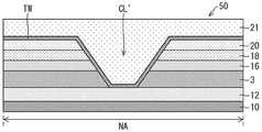
如图5中所示,在柔性有机EL显示装置50中,折弯狭缝CL’通过除去阻挡层3、无机绝缘膜16、无机绝缘膜18以及无机绝缘膜20 的所有无机层叠层来形成。As shown in FIG. 5 , in the flexible organic
在包含在柔性有机EL显示装置50的折弯狭缝CL’中,其侧面以较陡峭的锥形形状(倾斜形状)来形成,若以与折弯狭缝CL’正交的方式,对多个引绕配线TW进行图案化设置,则有如下问题:因较陡峭的锥形形状(倾斜形状)的侧面的影响,在多个引绕配线TW 之间的区域容易产生残留物,而且容易产生在多个引绕配线TW之间的裂纹。In the bending slit CL' included in the flexible organic
〔实施方式二〕[Embodiment 2]
接下来,基于图6说明本发明的实施方式二。在本实施方式的柔性有机EL显示装置1c中,在使用与半导体膜15同一层来形成的蚀刻阻挡物膜(第一蚀刻阻挡物膜层)15a、15b的基础上,还在比蚀刻阻挡物膜15a、15b更靠上层包含G3、G4,由与源极电极GE同一层的蚀刻阻挡物膜(第二蚀刻阻挡物膜层)的方面,与实施方式一不同,关于其他,如在实施方式一说明。为了便于说明,对与在特定的实施方式中说明的构成具有相同功能的构成标注相同的附图标记,省略其说明。Next,
图6的(a)是表示形成在包含顶栅型TFT元件的柔性有机EL显示装置1c的边框区域NA的折弯狭缝CL的剖视图,图6的(b)是表示包含在柔性有机EL显示装置1c的一部分的蚀刻阻挡物膜G3、 G4的形状的图。此外,在图6的(b)中,省略了蚀刻阻挡物膜 15a、15b的图示。FIG. 6( a ) is a cross-sectional view showing a bending slit CL formed in a frame region NA of a flexible organic
如图6的(a)所示,在狭缝CL中的靠近显示区域DA的一方的端部以及靠近端子部TM的一方的端部的两方中,形成有包含蚀刻阻挡物膜15a、15b、G3、G4的阶段形状的侧面。As shown in FIG. 6( a ), in the slit CL, the one end portion close to the display area DA and the one end portion close to the terminal portion TM are formed with
即,如图6的(a)中所示,在下表面膜10以及树脂层12上形成有至少包含阻挡层(第一无机膜层)3、比阻挡层3更靠上层的无机绝缘膜(第二无机膜层)16、比无机绝缘膜16更靠上层的无机绝缘膜(第三无机膜层)18的多个无机膜层,在上述多个无机膜层形成有狭缝CL。That is, as shown in FIG. 6( a ), on the
狭缝CL包含:第一狭缝,形成在多个引绕配线TW的延伸方向中的宽度是W1的阻挡层(第一无机膜层)3;第二狭缝,形成在多个引绕配线TW的延伸方向中的宽度是W2的无机绝缘膜(第二无机膜层)16;第三狭缝,形成在多个引绕配线TW的延伸方向中的宽度是W3的无机绝缘膜(第三无机膜层)18。The slit CL includes a first slit formed in the barrier layer (first inorganic film layer) 3 having a width W1 in the extending direction of the plurality of lead wires TW, and a second slit formed in the plurality of lead wires TW Inorganic insulating film (second inorganic film layer) 16 whose width in the extending direction of the wiring TW is W2; third slit, an inorganic insulating film whose width in the extending direction of the plurality of lead wires TW is W3 (Third inorganic film layer) 18 .
在多个引绕配线TW的延伸方向中的上述第一狭缝的两方的端部中,在阻挡层(第一无机膜层)3上形成有蚀刻阻挡物膜(第一蚀刻阻挡物层)15a、15b,在上述第二狭缝的多个引绕配线TW的延伸方向中的宽度W2宽于上述第一狭缝的多个引绕配线TW的延伸方向中的宽度W1。At both ends of the first slit in the extending direction of the plurality of lead wires TW, an etching stopper film (first etching stopper) is formed on the stopper layer (first inorganic film layer) 3 Layers) 15a and 15b, the width W2 in the extending direction of the plurality of lead wires TW of the second slit is wider than the width W1 in the extending direction of the plurality of lead wires TW of the first slit.
进一步,在多个引绕配线TW的延伸方向中的上述第二狭缝的两方的端部中,在无机绝缘膜(第二无机膜层)16上形成有蚀刻阻挡物膜(第二蚀刻阻挡物膜层)G3、G4,在上述第三狭缝的多个引绕配线TW的延伸方向中的宽度W3宽于上述第二狭缝的多个引绕配线TW的延伸方向中的宽度W2。Further, at both ends of the second slit in the extending direction of the plurality of lead wires TW, an etching stopper film (second inorganic film layer) is formed on the inorganic insulating film (second inorganic film layer) 16 . The etching stopper film layers) G3 and G4 have a width W3 in the extending direction of the plurality of lead wires TW of the third slit wider than the extending direction of the plurality of lead wires TW of the second slit. The width W2.
另外,如图6的(a)中所示,包含蚀刻阻挡物膜(第二蚀刻阻挡物膜层)G3、G4的上述第二狭缝的两方的端部中的上述第二狭缝的侧面和蚀刻阻挡物膜G3、G4的侧面也可以对齐。In addition, as shown in FIG. 6( a ), the second slit includes the etching stopper films (second etching stopper film layers) G3 and G4 at both ends of the second slit. The side surfaces and the side surfaces of the etch stopper films G3, G4 may also be aligned.
另外,如图6的(a)中所示,每个引绕配线TW1~TWn以与狭缝CL正交的方式形成,每个引绕配线TW1~TWn与蚀刻阻挡物膜 15a、15b、G3、G4相接。In addition, as shown in (a) of FIG. 6 , each of the lead wires TW1 to TWn is formed so as to be orthogonal to the slit CL, and each of the lead wires TW1 to TWn is connected to the
此外,在柔性有机EL显示装置1c的情况下,在狭缝CL中的靠近显示区域DA的一方的端部以及靠近端子部TM的一方的端部的两方中形成了包含刻阻挡物膜15a、15b、G3、G4的阶段形状的侧面,但也可以形成在只任一方。Further, in the case of the flexible organic
另外,在靠近显示区域DA的一方的端部中可以形成只包含蚀刻阻挡物膜(第一蚀刻阻挡物层)15a的阶段形状的侧面,在靠近端子部TM的一方的端部中也可以形成只包含蚀刻阻挡物膜(第二蚀刻阻挡物层)G4的阶段形状的侧面,靠近显示区域DA的一方的端部中可以形成只包含蚀刻阻挡物膜(第二蚀刻阻挡物层)G3的阶段形状的侧面,靠近端子部TM的一方的端部中也可以形成只包含蚀刻阻挡物膜(第一蚀刻阻挡物层)15b的阶段形状的侧面。In addition, a step-shaped side surface including only the etching stopper film (first etching stopper layer) 15a may be formed at one end near the display area DA, and may be formed at one end near the terminal portion TM The side surface of the stage shape including only the etch stopper film (second etch stopper layer) G4, and the end portion of the side near the display area DA can form a stage including only the etch stopper film (second etch stopper layer) G3 As for the side surface of the shape, the side surface of the step shape including only the etching stopper film (first etching stopper layer) 15b may be formed at one end portion close to the terminal portion TM.
另外,在狭缝CL中的靠近显示区域DA的一方的端部以及靠近端子部TM的一方的端部的两方中可以形成只包含蚀刻阻挡物膜(第一蚀刻阻挡物膜层)G3、G4的阶段形状的侧面,也可以形成在只任一方。In addition, the slit CL may be formed to include only the etch stopper film (first etch stopper film layer) G3, The side surface of the step shape of G4 may be formed on only one of them.
此外,由与栅极电极GE同一层的蚀刻阻挡物膜G3、G4是导电膜,由此,如图6的(b)中所示,每个蚀刻阻挡物膜G3、G4的形状由沿着狭缝CL的侧面形成的多个岛状的膜来形成,每个上述多个岛状的膜与每个引绕配线TW1~TWn接触,即,上述多个岛状的膜的每一个和引绕配线TW1~TWn的的每一个需要以逐一接触的方式形成。In addition, the etching stopper films G3, G4 of the same layer as the gate electrode GE are conductive films, whereby, as shown in (b) of FIG. 6, the shape of each etching stopper film G3, G4 is determined along the A plurality of island-shaped films formed on the side surfaces of the slit CL are formed, and each of the plurality of island-shaped films is in contact with each of the lead wires TW1 to TWn, that is, each of the plurality of island-shaped films and Each of the lead wires TW1 to TWn needs to be formed in contact one by one.
〔实施方式三〕[Embodiment 3]
接下来,基于图7说明本发明的实施方式三。在本实施方式的柔性有机EL显示装置1d中,在由与半导体膜15同一层来形成的蚀刻阻挡物膜(第一蚀刻阻挡物膜层)15a、15b和由与栅极电极GE同一层来形成的蚀刻阻挡物膜(第二蚀刻阻挡物膜层)G3、G4的基础上,还在比蚀刻阻挡物膜15a、15b、G3、G4更靠上层包含蚀刻阻挡物膜(第三蚀刻阻挡物层)C1、C2,蚀刻阻挡物膜(第三蚀刻阻挡物层)C1、C2由与电容电极CE同一层来形成的方面,与实施方式一以及实施方式一二不同,关于其他,如在实施方式一以及实施方式二说明。为了便于说明,对与在实施方式一以及实施方式二中说明的构成具有相同功能的构成标注相同的附图标记,省略其说明。Next,
图7的(a)是表示形成在包含顶栅型的TFT元件的柔性有机EL 显示装置1d的边框区域NA的折弯狭缝CL的剖视图,图7的(b) 是表示包含在柔性有机EL显示装置1d的一部分的蚀刻阻挡物膜 C1、C2的形状的图。此外,在图7的(b)中,省略了蚀刻阻挡物膜15a、15b、G3、G4的图示。FIG. 7( a ) is a cross-sectional view showing a folded slit CL formed in a frame region NA of a flexible organic
如图7的(a)中所示,在狭缝CL中的靠近显示区域DA的一方的端部以及靠近端子部TM的一方的端部的两方中,形成有包含蚀刻阻挡物膜15a、15b、G3、G4、C1、C2的阶段形状的侧面。As shown in FIG. 7( a ), in both of the end portion of the slit CL near the display area DA and the end portion of the one near the terminal portion TM, there are formed an
如图7的(a)中所示,在下表面膜10以及树脂层12上形成至少包含阻挡层(第一无机膜层)3、比阻挡层3更靠上层的无机绝缘膜 (第二无机膜层)16、比无机绝缘膜16更靠上层的无机绝缘膜(第三无机膜层)18、比无机绝缘膜18更靠上层的无机绝缘膜(第四无机膜层)20的多个无机膜层,在上述多个无机膜层形成有狭缝CL。As shown in FIG. 7( a ), on the
狭缝CL包含:第一狭缝,形成在多个引绕配线TW的延伸方向中的宽度是W1的阻挡层(第一无机膜层)3;第二狭缝,形成在多个引绕配线TW的延伸方向中的宽度是W2的无机绝缘膜(第二无机膜层)16;第三狭缝,形成在多个引绕配线TW的延伸方向中的宽度是W3的无机绝缘膜(第三无机膜层)18;第四狭缝,形成在多个引绕配线TW的延伸方向中的宽度是W4的无机绝缘膜(第四无机膜层)20。The slit CL includes a first slit formed in the barrier layer (first inorganic film layer) 3 having a width W1 in the extending direction of the plurality of lead wires TW, and a second slit formed in the plurality of lead wires TW Inorganic insulating film (second inorganic film layer) 16 whose width in the extending direction of the wiring TW is W2; third slit, an inorganic insulating film whose width in the extending direction of the plurality of lead wires TW is W3 (Third inorganic film layer) 18; Fourth slit, an inorganic insulating film (fourth inorganic film layer) 20 whose width in the extending direction of the plurality of lead wires TW is W4 is formed.
在多个引绕配线TW的延伸方向中的上述第一狭缝的两方的端部中,在阻挡层(第一无机膜层)3上形成有蚀刻阻挡物膜(第一蚀刻阻挡物层)15a、15b,在上述第二狭缝的多个引绕配线TW的延伸方向中的宽度W2宽于上述第一狭缝的多个引绕配线TW的延伸方向中的宽度W1。At both ends of the first slit in the extending direction of the plurality of lead wires TW, an etching stopper film (first etching stopper) is formed on the stopper layer (first inorganic film layer) 3 Layers) 15a and 15b, the width W2 in the extending direction of the plurality of lead wires TW of the second slit is wider than the width W1 in the extending direction of the plurality of lead wires TW of the first slit.
在多个引绕配线TW的延伸方向中的上述第二狭缝的两方的端部中,在无机绝缘膜(第二无机膜层)16上形成有蚀刻阻挡物膜(第二蚀刻阻挡物膜层)G3、G4,在上述第三狭缝的多个引绕配线TW 的延伸方向中的宽度W3宽于上述第二狭缝的多个引绕配线TW的延伸方向中的宽度W2。At both ends of the second slit in the extending direction of the plurality of lead wires TW, an etching stopper film (second etching stopper) is formed on the inorganic insulating film (second inorganic film layer) 16 (substance film layers) G3 and G4, the width W3 in the extending direction of the plurality of lead wires TW of the third slit is wider than the width of the plurality of lead wires TW of the second slit in the extending direction w2.
进一步,在多个引绕配线TW的延伸方向中的上述第三狭缝的两方的端部中,在无机绝缘膜(第三无机膜层)18上形成有蚀刻阻挡物膜(第三蚀刻阻挡物膜层)C1、C2,在上述第四狭缝的多个引绕配线TW的延伸方向中的宽度W4宽于上述第三狭缝的多个引绕配线TW的延伸方向中的宽度W3。Further, at both ends of the third slit in the extending direction of the plurality of lead wires TW, an etch stopper film (third inorganic film layer) is formed on the inorganic insulating film (third inorganic film layer) 18 The etching stopper film layers) C1 and C2 have a wider width W4 in the extending direction of the plurality of lead wires TW of the fourth slit than in the extending direction of the plurality of lead wires TW of the third slit. The width W3.
另外,如图7的(a)中所示,包含蚀刻阻挡物膜(第三蚀刻阻挡物膜层)C1、C2的上述第三狭缝的两方的端部中的上述第三狭缝的侧面和蚀刻阻挡物膜C1、C2的侧面也可以对齐。In addition, as shown in FIG. 7( a ), the etch stopper films (third etch stopper film layers) C1 and C2 are included in the third slit at both ends of the third slit. The sides and the sides of the etch stopper films C1, C2 may also be aligned.
另外,如图7的(a)中所示,每个引绕配线TW1~TWn以与狭缝CL正交的方式形成,每个引绕配线TW1~TWn与蚀刻阻挡物膜 15a、15b、G3、G4、C1、C2接触。In addition, as shown in (a) of FIG. 7 , each of the lead wires TW1 to TWn is formed so as to be orthogonal to the slit CL, and each of the lead wires TW1 to TWn is connected to the
此外,在柔性有机EL显示装置1d的情况下,在狭缝CL中的靠近显示区域DA的一方的端部以及靠近端子部TM的一方的端部的两方中形成了包含蚀刻阻挡物膜15a、15b、G3、G4、C1、C2的阶段形状的侧面,但也可以形成在只任一方。Further, in the case of the flexible organic
另外,在狭缝CL中的、靠近显示区域DA的一方的端部以及靠近端子部TM的一方的端部的两方中也可以形成只包含蚀刻阻挡物膜15a、15b或只包含蚀刻阻挡膜G3、G4或只包含蚀刻阻挡膜 C1、C2的阶段形状的侧面,也可以形成在只任一方。In addition, only the
此外,由与电容电极CE同一层来形成的蚀刻阻挡物膜C1、C2是导电膜,由此,如图7的(b)中所示,每个蚀刻阻挡物膜C1、C2 的形状由沿着狭缝CL的侧面形成的多个岛状的膜来形成,每个上述多个岛状的膜与每个引绕配线TW1~TWn接触,即,每个上述多个岛状的膜和每个引绕配线TW1~TWn也需要以逐一接触的方式形成。Further, the etching stopper films C1, C2 formed of the same layer as the capacitance electrode CE are conductive films, whereby, as shown in (b) of FIG. 7, the shape of each etching stopper film C1, C2 is determined by the The plurality of island-shaped films are formed along the side surfaces of the slits CL, and each of the plurality of island-shaped films is in contact with each of the lead wires TW1 to TWn, that is, each of the plurality of island-shaped films and Each of the lead wires TW1 to TWn also needs to be formed in contact one by one.
〔实施方式四〕[Embodiment 4]
接下来,基于图8以及图9说明本发明的实施方式四。在本实施方式的柔性有机EL显示装置1e,在代替折弯狭缝CL包含裂纹的放大抑制用狭缝SL的方面,与实施方式一不同,关于其他,如在实施方式一说明。为了便于说明,对与在实施方式一中说明的构成具有相同功能的构成标注相同的附图标记,省略其说明。Next,
图8是用于说明包含顶栅型TFT元件的柔性有机EL显示装置1e 的概略构成的俯视图。FIG. 8 is a plan view for explaining a schematic configuration of a flexible organic EL display device 1e including a top-gate TFT element.
图9是表示形成在柔性有机EL显示装置1e的边框区域NA的裂纹的放大抑制用狭缝SL的剖视图。9 is a cross-sectional view showing a slit SL for suppressing enlargement of cracks formed in the frame region NA of the flexible organic EL display device 1e.
裂纹的放大抑制用狭缝SL的形成可以与上述折弯狭缝CL同样地形成,而在此省略其说明。The formation of the slit SL for suppressing the enlargement of the crack can be formed in the same manner as the above-mentioned bending slit CL, and the description thereof is omitted here.
在本实施方式的柔性有机EL显示装置1e中,由于可以抑制在通过各向异性导电膜来压接时等在端子部TM发生的裂纹扩散到显示区域DA侧,并且形成在边框区域NA的裂纹的放大抑制用狭缝SL 具有包含蚀刻阻挡物膜15a、15b的阶段形状的侧面,从而在对形成在狭缝SL内的引绕配线TW1~TWn进行图案化时,可以抑制在引绕配线TW1~TWn之间产生残留物,而且可以抑制在引绕配线 TW1~TWn之间产生漏电。In the flexible organic EL display device 1e of the present embodiment, cracks generated in the terminal portion TM during pressure-bonding with an anisotropic conductive film can be suppressed from spreading to the display region DA side and cracks formed in the frame region NA. The enlargement suppressing slit SL has a side surface with a stepped shape including the
此外,裂纹的放大抑制用狭缝SL和折弯狭缝CL能够以相同形状形成,由此也可以形成一个狭缝,并且也可以用作裂纹的放大抑制用和折弯用。In addition, the slits SL for suppressing the enlargement of cracks and the bending slits CL can be formed in the same shape, so that one slit can be formed, and the slits can also be used for suppressing the enlargement of cracks and for bending.
〔实施方式五〕[Embodiment 5]
接下来,基于图10说明本发明的实施方式五。在本实施方式的柔性有机EL显示装置1f、1g、1h,在包含底栅型TFT元件的方面,与实施方式一至实施方式四不同,关于其他,如在实施方式一至实施方式四说明。为了便于说明,对与在实施方式一至实施方式四中说明的构成具有相同功能的构成标注相同的附图标记,省略其说明。Next,
图10是表示形成在包含底栅型TFT元件的柔性有机EL显示装置 1f、1g、1h的边框区域NA的折弯狭缝CL的一个例子的剖视图。Fig. 10 is a cross-sectional view showing an example of a folded slit CL formed in the frame regions NA of the flexible organic EL display devices 1f, 1g, and 1h including bottom-gate TFT elements.
在图10的(a)中图示的柔性有机EL显示装置1f中,包含蚀刻阻挡物膜(第一蚀刻阻挡物层)15a、15b,其使用与包含在底栅型 TFT元件的半导体膜15同一层来形成,蚀刻阻挡物膜15a、15b形成在无机绝缘膜16上。In the flexible organic EL display device 1f illustrated in (a) of FIG. 10, etching stopper films (first etching stopper layers) 15a, 15b are included, which use the
在图10的(b)中图示的柔性有机EL显示装置1g中,在使用与包含在底栅型TFT元件的半导体膜15同一层来形成的蚀刻阻挡物膜(第二蚀刻阻挡物层)15a、15b的基础上,在比蚀刻阻挡物膜15a、 15b更靠下层还包含蚀刻阻挡物膜(第一蚀刻阻挡物层)G3、G4,其由与包含在底栅型TFT元件的栅极电极GE同一层来形成。In the flexible organic EL display device 1g illustrated in (b) of FIG. 10 , an etching stopper film (second etching stopper layer) formed using the same layer as the
在图10的(c)中图示的柔性有机EL显示装置1h中,在使用与包含在底栅型TFT元件的半导体膜15同一层来形成蚀刻阻挡物膜 (第二蚀刻阻挡物层)15a、15b、和使用与包含在底栅型TFT的栅极电极GE同一层来形成蚀刻阻挡物膜(第一蚀刻阻挡物层)G3、 G4的基础上,在比蚀刻阻挡物膜15a、15b、G3、G4更靠上层还包含蚀刻阻挡物膜(第三蚀刻阻挡物层)C1、C2,其由与电容电极CE 同一层来形成。In the flexible organic EL display device 1h illustrated in (c) of FIG. 10 , the etching stopper film (second etching stopper layer) 15a is formed using the same layer as the
〔总结〕〔Summarize〕
〔方式1〕[Method 1]
一种显示装置,其在基板上包含:A display device comprising on a substrate:
显示区域,包含多个显示元件以及多个有源元件;Display area, including multiple display elements and multiple active elements;
边框区域,设置在上述显示区域的周围,以及a border area, set around the aforementioned display area, and
多个引绕配线的每一个的端子部,设置在上述边框区域的端部,上述显示装置的特征在于,A terminal portion of each of the plurality of lead wires is provided at an end portion of the frame region, and the display device is characterized in that:
在上述基板上形成有至少包含第一无机膜层、比上述第一无机膜层上层的第二无机膜层的多个无机膜层,A plurality of inorganic film layers including at least a first inorganic film layer and a second inorganic film layer above the first inorganic film layer are formed on the substrate,
在边框区域中的上述显示区域和上述端子部之间,在上述多个无机膜层形成有狭缝,Slits are formed in the plurality of inorganic film layers between the display region and the terminal portion in the frame region,
上述狭缝包含形成在上述第一无机膜层的第一狭缝和形成在上述第二无机膜层的第二狭缝,The slit includes a first slit formed in the first inorganic film layer and a second slit formed in the second inorganic film layer,
在上述多个引绕配线的延伸方向中的上述第一狭缝的至少一方的端部中,在上述第一无机膜层上形成有第一蚀刻阻挡物膜层,A first etch stopper film layer is formed on the first inorganic film layer at an end portion of at least one of the first slits in the extending direction of the plurality of lead wires,
上述第二狭缝的上述多个引绕配线的延伸方向中的宽度宽于上述第一狭缝的上述多个引绕配线的延伸方向中的宽度。The width in the extending direction of the plurality of lead wires of the second slit is wider than the width of the first slit in the extending direction of the plurality of lead wires.
〔方式2〕[Method 2]
根据方式1所述的显示装置,其特征在于,The display device according to
上述多个引绕配线的延伸方向中的上述第一狭缝的两方的端部的每一个中,在上述第一无机膜层上形成有上述第一蚀刻阻挡物膜层。The first etch stopper film layer is formed on the first inorganic film layer in each of both end portions of the first slit in the extending direction of the plurality of lead wires.
〔方式3〕[Method 3]
根据方式1或2所述的显示装置,其特征在于,The display device according to
在包含上述第一蚀刻阻挡物层的上述第一狭缝的端部中,上述第一狭缝的侧面和上述第一蚀刻阻挡物膜层的侧面对齐。In the end portion of the first slit including the first etch stopper layer, the side surface of the first slit and the side surface of the first etch stopper film layer are aligned.
〔方式4〕[Method 4]
根据方式1至3中任一项所述的显示装置,其特征在于,The display device according to any one of
上述多个引绕配线是金属配线,The plurality of lead wires described above are metal wires,
上述多个引绕配线以与上述狭缝正交的方式形成,The plurality of lead wires are formed so as to be orthogonal to the slits,
上述多个引绕配线与上述第一蚀刻阻挡物膜层接触。The plurality of lead wires are in contact with the first etch stopper film.
〔方式5〕[Method 5]
根据方式4所述的显示装置,其特征在于,The display device according to
在上述基板上形成有第一树脂层,A first resin layer is formed on the above-mentioned substrate,
上述多个无机膜层形成在上述第一树脂层上,The plurality of inorganic film layers are formed on the first resin layer,
上述狭缝以露出上述第一树脂层的方式形成,The slit is formed so as to expose the first resin layer,
上述多个引绕配线的每一个的一部分,与上述第一树脂层接触而形成。A part of each of the plurality of lead wires is formed in contact with the first resin layer.
〔方式6〕[Method 6]
根据方式1至5中任一项所述的显示装置,其特征在于,The display device according to any one of
上述多个无机膜层包含比上述第二无机膜层上层的第三无机膜层,The plurality of inorganic film layers include a third inorganic film layer above the second inorganic film layer,
上述狭缝包含形成在上述第三无机膜层的第三狭缝,The slit includes a third slit formed in the third inorganic film layer,
在上述引绕配线的延伸方向中的上述第二狭缝的至少一方的端部中,在上述第二无机膜层上形成有第二蚀刻阻挡物膜,A second etch stopper film is formed on the second inorganic film layer at an end portion of at least one of the second slits in the extending direction of the lead wire,
上述第三狭缝的上述多个引绕配线的延伸方向中的宽度宽于上述第二狭缝的上述多个引绕配线的延伸方向中的宽度。The width in the extending direction of the plurality of lead wires of the third slit is wider than the width of the second slit in the extending direction of the plurality of lead wires.
〔方式7〕[Method 7]
根据方式6所述的显示装置,其特征在于,The display device according to
上述多个引绕配线的延伸方向中的上述第二狭缝的两方的端部的每一个中,在上述第二无机膜层上形成有上述第二蚀刻阻挡物膜层。The second etch stopper film layer is formed on the second inorganic film layer in each of both end portions of the second slit in the extending direction of the plurality of lead wires.
〔方式8〕[Method 8]
根据方式6或7所述的显示装置,其特征在于,The display device according to
在包含上述第二蚀刻阻挡物膜层的上述第二狭缝的端部中,上述第二狭缝的侧面和上述第二蚀刻阻挡物膜的侧面对齐。In the end portion of the second slit including the second etch stopper film layer, the side surface of the second slit and the side surface of the second etch stopper film are aligned.
〔方式9〕[Method 9]
根据方式6至8中任一项所述的显示装置,其特征在于,The display device according to any one of
上述多个无机膜层包含比上述第三无机膜层上层的第四无机膜层,The plurality of inorganic film layers include a fourth inorganic film layer above the third inorganic film layer,
上述狭缝包含形成在上述第四无机膜层的第四狭缝,The slit includes a fourth slit formed in the fourth inorganic film layer,
在上述多个引绕配线的延伸方向中的上述第三狭缝的至少一方的端部中,在上述第三无机膜层上形成有第三蚀刻阻挡物膜层,A third etch stopper film layer is formed on the third inorganic film layer at an end portion of at least one of the third slits in the extending direction of the plurality of lead wires,
上述第四狭缝的上述多个引绕配线的延伸方向中的宽度比上述第三狭缝的上述多个引绕配线的延伸方向中的宽度宽。The width in the extending direction of the plurality of lead wires of the fourth slit is wider than the width of the third slit in the extending direction of the plurality of lead wires.
〔方式10〕[Method 10]
根据方式9所述的显示装置,其特征在于,The display device according to aspect 9, wherein:
上述多个引绕配线的延伸方向中的上述第三狭缝的两方的端部的每一个中,在上述第三无机膜层上形成有上述第三蚀刻阻挡物膜层。The third etch stopper film layer is formed on the third inorganic film layer in each of both end portions of the third slit in the extending direction of the plurality of lead wires.
〔方式11〕[Method 11]
根据方式9或10中所述的显示装置,其特征在于,The display device according to
包含上述第三蚀刻阻挡物膜的上述第三狭缝的端部中,上述第三狭缝的侧面和上述第三蚀刻阻挡物膜层的侧面对齐。In the end portion of the third slit including the third etch stopper film, the side surface of the third slit and the side surface of the third etch stopper film layer are aligned.
〔方式12〕[Method 12]
根据方式9至11中任一项所述的显示装置,其特征在于,The display device according to any one of modes 9 to 11, wherein:
上述第一无机膜层是无机防潮层,The above-mentioned first inorganic film layer is an inorganic moisture-proof layer,
上述第二无机膜层与上述有源元件包含的栅极绝缘膜层同一层,The second inorganic film layer is the same layer as the gate insulating film layer included in the active element,
上述第三无机膜层与上述有源元件包含的第一无机绝缘膜同一层,The third inorganic film layer is the same layer as the first inorganic insulating film included in the active element,
上述第四无机膜层与上述有源元件包含的第二无机绝缘膜同一层。The fourth inorganic film layer is the same layer as the second inorganic insulating film included in the active element.
〔方式13〕[Method 13]
根据方式12所述的显示装置的制造方法,其特征在于,The method of manufacturing a display device according to
包含电容元件,上述电容元件包含形成在上述第三无机膜层和上述第四无机膜层之间的电容电极层,including a capacitor element, the capacitor element including a capacitor electrode layer formed between the third inorganic film layer and the fourth inorganic film layer,
上述第一蚀刻阻挡物膜层由从与上述有源元件包含的半导体层同一层以及与上述有源元件包含的栅极电极层同一层中选择的一方来形成,The first etch stopper film layer is formed of one selected from the same layer as the semiconductor layer included in the active element and the same layer as the gate electrode layer included in the active element,
上述第二蚀刻阻挡物膜层由从与上述有源元件包含的半导体层同一层以及与上述有源元件包含的栅极电极层同一层中选择的另一方来形成,The second etch stopper film layer is formed by the other selected from the same layer as the semiconductor layer included in the active element and the same layer as the gate electrode layer included in the active element,
上述第三蚀刻阻挡物膜层由上述电容电极层同一层来形成。The third etch stopper film layer is formed of the same layer as the capacitor electrode layer.
〔方式14〕[Method 14]
根据方式1至13中任一项所述的显示装置,其特征在于,The display device according to any one of
上述狭缝形成折弯部,上述多个引绕配线由第二树脂层覆盖。The slit forms a bent portion, and the plurality of lead wires are covered with the second resin layer.
〔方式15〕[Method 15]
根据方式1至14中任一项所述的显示装置,其特征在于,The display device according to any one of
上述第一蚀刻阻挡物膜层通过与上述有源元件包含的半导体层同一层来形成,The above-mentioned first etch stopper film layer is formed by the same layer as the semiconductor layer included in the above-mentioned active element,
上述第一蚀刻阻挡物膜层形成为一个岛状,The above-mentioned first etching stopper film layer is formed into an island shape,
上述一个岛状的第一蚀刻阻挡物膜层与上述多个引绕配线中的不同的两个以上接触。The one island-shaped first etch stopper film layer is in contact with two or more different ones of the plurality of lead wires.
〔方式16〕[Method 16]
根据方式1至14中任一项所述的显示装置,其特征在于,The display device according to any one of
上述第一蚀刻阻挡物膜层通过与上述有源元件包含的半导体层同一层来形成,The above-mentioned first etch stopper film layer is formed by the same layer as the semiconductor layer included in the above-mentioned active element,
上述第一蚀刻阻挡物层形成为多个岛状,The above-mentioned first etching stopper layer is formed in a plurality of island shapes,
上述多个岛状的第一蚀刻阻挡物层的每一个与上述多个引绕配线中的不同的一个相接。Each of the plurality of island-shaped first etch stopper layers is in contact with a different one of the plurality of lead wires.
〔方式17〕[Method 17]
根据方式1至14中任一项所述的显示装置,其特征在于,The display device according to any one of
上述第一蚀刻阻挡物膜层由上述有源元件包含的半导体层同一层来形成,The above-mentioned first etch stopper film layer is formed of the same layer as the semiconductor layer included in the above-mentioned active element,
上述第一蚀刻阻挡物膜层形成为多个岛状,The above-mentioned first etch stopper film layer is formed into a plurality of island shapes,
上述多个岛状的第一蚀刻阻挡物膜层的至少一个与上述多个引绕配线中的不同的两个以上接触。At least one of the plurality of island-shaped first etch stopper film layers is in contact with two or more different ones of the plurality of lead wires.
〔方式18〕[Method 18]
根据方式1至14中任一项所述的显示装置,其特征在于,The display device according to any one of
上述第一蚀刻阻挡物膜层通过金属层来形成,The above-mentioned first etching stopper film layer is formed by a metal layer,
上述第一蚀刻阻挡物膜层形成为多个岛状,The above-mentioned first etch stopper film layer is formed into a plurality of island shapes,
上述多个岛状的第一蚀刻阻挡物膜层的每一个与上述多个引绕配线中的不同的一个接触。Each of the plurality of island-shaped first etch stopper film layers is in contact with a different one of the plurality of lead wires.
〔方式19〕[Method 19]
根据方式1至18中任一项所述的显示装置,其特征在于,The display device according to any one of
上述狭缝在上述基板上从与上述多个引绕配线的延伸方向正交的方向的一方侧的端部形成到另一方侧的端部,The slit is formed on the substrate from an end portion on one side to an end portion on the other side in a direction orthogonal to the extending direction of the plurality of lead wires,
上述第一蚀刻阻挡物层形成在比上述一方侧的端部以及上述另一方侧的端部更内侧。The first etch stopper layer is formed on the inner side of the end portion on the one side and the end portion on the other side.
〔附记事项〕[Additional Matters]
本发明不限于上述的各实施方式,在权利要求所示的范围中能够进行各种变更,将分别公开在不同的实施方式中的技术手段适当组合而得到的实施方式也包含在本发明的技术范围中。而且,通过将各实施方式中分别公开的技术手段组合能够形成新的技术特征。The present invention is not limited to the above-described embodiments, and various modifications can be made within the scope of the claims, and embodiments obtained by appropriately combining technical means disclosed in different embodiments are also included in the technology of the present invention. in the range. Furthermore, new technical features can be formed by combining the technical means disclosed in the respective embodiments.
工业上的实用性Industrial applicability
本发明可以利用于显示装置The present invention can be applied to a display device
附图标记说明Description of reference numerals
1、1a~1h柔性有机EL显示装置,3阻挡层,4TFT层,5有机EL元件层,6密封层,12树脂层,16、18、20无机绝缘膜,21 平坦化膜,CL折弯狭缝,SL裂纹的放大抑制用狭缝,DA显示区域,NA边框区域,TM端子部,TW1~TWn引绕配线,Tr薄膜晶体管,GE栅极电极,SH源极、漏极配线,CE电容电极,15a、 15b、G3、G4、C1、C2蚀刻阻挡物膜,SH1第一导电构件,SH2 第二导电构件,G1第三导电构件,G2第四导构件。1. 1a~1h flexible organic EL display device, 3 barrier layer, 4TFT layer, 5 organic EL element layer, 6 sealing layer, 12 resin layer, 16, 18, 20 inorganic insulating film, 21 flattening film, CL bending narrow Slit, Slit for SL crack amplification suppression, DA display area, NA frame area, TM terminal, TW1 to TWn lead wire, Tr TFT, GE gate electrode, SH source and drain wire, CE Capacitor electrodes, 15a, 15b, G3, G4, C1, C2 etch stopper film, SH1 first conductive member, SH2 second conductive member, G1 third conductive member, G2 fourth conductive member.
Claims (19)
Applications Claiming Priority (1)
| Application Number | Priority Date | Filing Date | Title |
|---|---|---|---|
| PCT/JP2018/003259WO2019150503A1 (en) | 2018-01-31 | 2018-01-31 | Display device |
Publications (2)
| Publication Number | Publication Date |
|---|---|
| CN111656427Atrue CN111656427A (en) | 2020-09-11 |
| CN111656427B CN111656427B (en) | 2022-02-22 |
Family
ID=67478406
Family Applications (1)
| Application Number | Title | Priority Date | Filing Date |
|---|---|---|---|
| CN201880087601.7AActiveCN111656427B (en) | 2018-01-31 | 2018-01-31 | Display device |
Country Status (3)
| Country | Link |
|---|---|
| US (1) | US11574982B2 (en) |
| CN (1) | CN111656427B (en) |
| WO (1) | WO2019150503A1 (en) |
Families Citing this family (6)
| Publication number | Priority date | Publication date | Assignee | Title |
|---|---|---|---|---|
| JP6843710B2 (en)* | 2017-07-12 | 2021-03-17 | 株式会社ジャパンディスプレイ | Display device and manufacturing method of display device |
| JP7068800B2 (en)* | 2017-10-30 | 2022-05-17 | 株式会社ジャパンディスプレイ | Display device |
| CN111725279B (en)* | 2020-06-11 | 2022-10-04 | 武汉华星光电半导体显示技术有限公司 | Array substrate and OLED display panel |
| KR20230039795A (en)* | 2021-09-13 | 2023-03-22 | 삼성디스플레이 주식회사 | Display device and method of manufacturing the same |
| WO2024157342A1 (en)* | 2023-01-24 | 2024-08-02 | シャープディスプレイテクノロジー株式会社 | Display device and method for manufacturing same |
| US20240389404A1 (en)* | 2023-05-15 | 2024-11-21 | Samsung Display Co., Ltd. | Display panel and electronic apparatus including the same |
Citations (19)
| Publication number | Priority date | Publication date | Assignee | Title |
|---|---|---|---|---|
| JP2003045516A (en)* | 2001-08-03 | 2003-02-14 | Stanley Electric Co Ltd | Clip terminal and liquid crystal display device having the clip terminal |
| CN1525553A (en)* | 2003-02-26 | 2004-09-01 | ���µ�����ҵ��ʽ���� | Manufacturing method of semiconductor device |
| JP2006237534A (en)* | 2005-02-28 | 2006-09-07 | Sony Corp | Semiconductor device and method for manufacturing semiconductor device |
| CN1841762A (en)* | 2005-03-21 | 2006-10-04 | 三星Sdi株式会社 | Light emitting display and manufacturing method thereof |
| JP2010267735A (en)* | 2009-05-13 | 2010-11-25 | Sharp Corp | Nitride semiconductor laser device, optical disk device, and image display device |
| CN102405686A (en)* | 2010-04-19 | 2012-04-04 | 松下电器产业株式会社 | Organic electroluminescence display panel, organic electroluminescence display device including the organic electroluminescence display panel, and method for manufacturing the organic electroluminescence display panel |
| CN102652330A (en)* | 2009-12-09 | 2012-08-29 | 夏普株式会社 | Semiconductor device and method for producing same |
| CN103210698A (en)* | 2011-11-16 | 2013-07-17 | 松下电器产业株式会社 | Manufacturing method of display panel and display panel |
| CN104183600A (en)* | 2013-05-28 | 2014-12-03 | 乐金显示有限公司 | Flexible display device and manufacturing method thereof |
| US20150014680A1 (en)* | 2013-07-10 | 2015-01-15 | Semiconductor Energy Laboratory Co., Ltd. | Semiconductor device and display device including the semiconductor device |
| JP2015060750A (en)* | 2013-09-19 | 2015-03-30 | 株式会社ジャパンディスプレイ | ORGANIC ELECTROLUMINESCENT DISPLAY DEVICE AND METHOD FOR PRODUCING ORGANIC ELECTROLUMINESCENT DISPLAY DEVICE |
| CN104966718A (en)* | 2015-05-04 | 2015-10-07 | 深圳市华星光电技术有限公司 | Manufacturing method of AMOLED backboard and AMOLED backboard structure |
| US20160062193A1 (en)* | 2014-09-01 | 2016-03-03 | Mitsubishi Electric Corporation | Liquid crystal display panel and method of manufacturing the same |
| CN205450518U (en)* | 2014-12-25 | 2016-08-10 | 株式会社日本显示器 | Display device |
| CN106129064A (en)* | 2016-05-25 | 2016-11-16 | 友达光电股份有限公司 | Active element array substrate |
| US20170062619A1 (en)* | 2015-08-26 | 2017-03-02 | Semiconductor Energy Laboratory Co., Ltd. | Semiconductor device and manufacturing method thereof |
| CN107006088A (en)* | 2014-12-10 | 2017-08-01 | 乐金显示有限公司 | Flexible display devices with various micro-coatings |
| CN107026121A (en)* | 2017-05-17 | 2017-08-08 | 京东方科技集团股份有限公司 | Preparation method, array base palte and the display device of array base palte |
| CN107454981A (en)* | 2016-07-25 | 2017-12-08 | 深圳市柔宇科技有限公司 | The manufacture method of array base palte and array base palte |
Family Cites Families (12)
| Publication number | Priority date | Publication date | Assignee | Title |
|---|---|---|---|---|
| BR112012002178A2 (en)* | 2009-07-28 | 2016-05-31 | Sharp Kk | wiring board, method of fabrication, display panel, and display device |
| US9543370B2 (en)* | 2014-09-24 | 2017-01-10 | Apple Inc. | Silicon and semiconducting oxide thin-film transistor displays |
| US10651253B2 (en)* | 2014-10-16 | 2020-05-12 | Sharp Kabushiki Kaisha | Light emitting element, display panel, display device, electronic device and method for producing light emitting element |
| KR102381285B1 (en)* | 2015-08-06 | 2022-03-31 | 삼성디스플레이 주식회사 | Flexible display device and manufacturing method thereof |
| KR102443703B1 (en)* | 2015-09-30 | 2022-09-16 | 삼성디스플레이 주식회사 | Display device and manufacturing method thereof |
| TWI740908B (en)* | 2016-03-11 | 2021-10-01 | 南韓商三星顯示器有限公司 | Display apparatus |
| JP6872343B2 (en)* | 2016-10-18 | 2021-05-19 | 株式会社ジャパンディスプレイ | Display device and manufacturing method of display device |
| JP2018078057A (en)* | 2016-11-11 | 2018-05-17 | 株式会社ジャパンディスプレイ | Display device |
| JP6777558B2 (en)* | 2017-01-20 | 2020-10-28 | 株式会社ジャパンディスプレイ | Display device |
| KR102333671B1 (en)* | 2017-05-29 | 2021-12-01 | 삼성디스플레이 주식회사 | Organic light emitting display device and a method of manufacturing organic light emitting display device |
| WO2019026237A1 (en)* | 2017-08-03 | 2019-02-07 | シャープ株式会社 | Display device |
| CN110137186B (en)* | 2019-05-30 | 2021-12-28 | 京东方科技集团股份有限公司 | Flexible display substrate and manufacturing method thereof |
- 2018
- 2018-01-31USUS16/964,852patent/US11574982B2/enactiveActive
- 2018-01-31WOPCT/JP2018/003259patent/WO2019150503A1/ennot_activeCeased
- 2018-01-31CNCN201880087601.7Apatent/CN111656427B/enactiveActive
Patent Citations (19)
| Publication number | Priority date | Publication date | Assignee | Title |
|---|---|---|---|---|
| JP2003045516A (en)* | 2001-08-03 | 2003-02-14 | Stanley Electric Co Ltd | Clip terminal and liquid crystal display device having the clip terminal |
| CN1525553A (en)* | 2003-02-26 | 2004-09-01 | ���µ�����ҵ��ʽ���� | Manufacturing method of semiconductor device |
| JP2006237534A (en)* | 2005-02-28 | 2006-09-07 | Sony Corp | Semiconductor device and method for manufacturing semiconductor device |
| CN1841762A (en)* | 2005-03-21 | 2006-10-04 | 三星Sdi株式会社 | Light emitting display and manufacturing method thereof |
| JP2010267735A (en)* | 2009-05-13 | 2010-11-25 | Sharp Corp | Nitride semiconductor laser device, optical disk device, and image display device |
| CN102652330A (en)* | 2009-12-09 | 2012-08-29 | 夏普株式会社 | Semiconductor device and method for producing same |
| CN102405686A (en)* | 2010-04-19 | 2012-04-04 | 松下电器产业株式会社 | Organic electroluminescence display panel, organic electroluminescence display device including the organic electroluminescence display panel, and method for manufacturing the organic electroluminescence display panel |
| CN103210698A (en)* | 2011-11-16 | 2013-07-17 | 松下电器产业株式会社 | Manufacturing method of display panel and display panel |
| CN104183600A (en)* | 2013-05-28 | 2014-12-03 | 乐金显示有限公司 | Flexible display device and manufacturing method thereof |
| US20150014680A1 (en)* | 2013-07-10 | 2015-01-15 | Semiconductor Energy Laboratory Co., Ltd. | Semiconductor device and display device including the semiconductor device |
| JP2015060750A (en)* | 2013-09-19 | 2015-03-30 | 株式会社ジャパンディスプレイ | ORGANIC ELECTROLUMINESCENT DISPLAY DEVICE AND METHOD FOR PRODUCING ORGANIC ELECTROLUMINESCENT DISPLAY DEVICE |
| US20160062193A1 (en)* | 2014-09-01 | 2016-03-03 | Mitsubishi Electric Corporation | Liquid crystal display panel and method of manufacturing the same |
| CN107006088A (en)* | 2014-12-10 | 2017-08-01 | 乐金显示有限公司 | Flexible display devices with various micro-coatings |
| CN205450518U (en)* | 2014-12-25 | 2016-08-10 | 株式会社日本显示器 | Display device |
| CN104966718A (en)* | 2015-05-04 | 2015-10-07 | 深圳市华星光电技术有限公司 | Manufacturing method of AMOLED backboard and AMOLED backboard structure |
| US20170062619A1 (en)* | 2015-08-26 | 2017-03-02 | Semiconductor Energy Laboratory Co., Ltd. | Semiconductor device and manufacturing method thereof |
| CN106129064A (en)* | 2016-05-25 | 2016-11-16 | 友达光电股份有限公司 | Active element array substrate |
| CN107454981A (en)* | 2016-07-25 | 2017-12-08 | 深圳市柔宇科技有限公司 | The manufacture method of array base palte and array base palte |
| CN107026121A (en)* | 2017-05-17 | 2017-08-08 | 京东方科技集团股份有限公司 | Preparation method, array base palte and the display device of array base palte |
Non-Patent Citations (2)
| Title |
|---|
| CMA ASHRUF: "A new contactless electrochemical etch-stop based on a gold/silicon/TMAH galvanic cell", 《SENSORS AND ACTUATORS A PHYSICAL》* |
| XXJDUK80: "采用in-film结构刻蚀阻挡层进行双镶嵌刻蚀工艺的研究", 《豆丁》* |
Also Published As
| Publication number | Publication date |
|---|---|
| US20210066440A1 (en) | 2021-03-04 |
| CN111656427B (en) | 2022-02-22 |
| US11574982B2 (en) | 2023-02-07 |
| WO2019150503A1 (en) | 2019-08-08 |
Similar Documents
| Publication | Publication Date | Title |
|---|---|---|
| CN111033782B (en) | Display device, method of manufacturing display device, and apparatus for manufacturing display device | |
| US10809553B2 (en) | Flexible substrate | |
| CN111656427B (en) | Display device | |
| JP7064846B2 (en) | Display device and manufacturing method of display device | |
| US20200119131A1 (en) | Display device | |
| US11800755B2 (en) | Display device | |
| WO2019021466A1 (en) | Display device, display device manufacturing method, and display device manufacturing apparatus | |
| JP6457879B2 (en) | Display device and manufacturing method thereof | |
| JP2017123217A (en) | Organic EL display device | |
| CN111108541B (en) | Flexible display device and manufacturing method of flexible display device | |
| CN111149431A (en) | Display device, method for manufacturing display device, and device for manufacturing display device | |
| WO2019021467A1 (en) | Display device, display device manufacturing method, and display device manufacturing apparatus | |
| US20210005701A1 (en) | Display device | |
| US20200335725A1 (en) | Display device, and manufacturing method of display device | |
| CN111868809B (en) | Display device and method for manufacturing display device | |
| US11462700B2 (en) | Display device comprising flexible display panel | |
| CN111902855A (en) | Method for manufacturing display device and display device | |
| WO2018179175A1 (en) | Display device, display device production method, display device production apparatus, deposition apparatus, and controller | |
| CN112753059B (en) | Display device | |
| US12207503B2 (en) | Display device | |
| US11404525B2 (en) | Display device and method for manufacturing display device | |
| CN111133496B (en) | Display device, method of manufacturing display device, and apparatus for manufacturing display device | |
| WO2021009811A1 (en) | Display device | |
| WO2020202281A1 (en) | Display device | |
| WO2019167280A1 (en) | Display device manufacturing method and mother board for display devices |
Legal Events
| Date | Code | Title | Description |
|---|---|---|---|
| PB01 | Publication | ||
| PB01 | Publication | ||
| SE01 | Entry into force of request for substantive examination | ||
| SE01 | Entry into force of request for substantive examination | ||
| GR01 | Patent grant | ||
| GR01 | Patent grant |