CN111656235A - Waveguides and Waveguide-Based Sensors - Google Patents
Waveguides and Waveguide-Based SensorsDownload PDFInfo
- Publication number
- CN111656235A CN111656235ACN201880087583.2ACN201880087583ACN111656235ACN 111656235 ACN111656235 ACN 111656235ACN 201880087583 ACN201880087583 ACN 201880087583ACN 111656235 ACN111656235 ACN 111656235A
- Authority
- CN
- China
- Prior art keywords
- core
- waveguide
- cladding
- region
- cross
- Prior art date
- Legal status (The legal status is an assumption and is not a legal conclusion. Google has not performed a legal analysis and makes no representation as to the accuracy of the status listed.)
- Pending
Links
Images


Classifications
- G—PHYSICS
- G02—OPTICS
- G02B—OPTICAL ELEMENTS, SYSTEMS OR APPARATUS
- G02B6/00—Light guides; Structural details of arrangements comprising light guides and other optical elements, e.g. couplings
- G02B6/10—Light guides; Structural details of arrangements comprising light guides and other optical elements, e.g. couplings of the optical waveguide type
- G02B6/12—Light guides; Structural details of arrangements comprising light guides and other optical elements, e.g. couplings of the optical waveguide type of the integrated circuit kind
- G02B6/122—Basic optical elements, e.g. light-guiding paths
- G02B6/1221—Basic optical elements, e.g. light-guiding paths made from organic materials
- G—PHYSICS
- G01—MEASURING; TESTING
- G01L—MEASURING FORCE, STRESS, TORQUE, WORK, MECHANICAL POWER, MECHANICAL EFFICIENCY, OR FLUID PRESSURE
- G01L1/00—Measuring force or stress, in general
- G01L1/24—Measuring force or stress, in general by measuring variations of optical properties of material when it is stressed, e.g. by photoelastic stress analysis using infrared, visible light, ultraviolet
- G—PHYSICS
- G01—MEASURING; TESTING
- G01B—MEASURING LENGTH, THICKNESS OR SIMILAR LINEAR DIMENSIONS; MEASURING ANGLES; MEASURING AREAS; MEASURING IRREGULARITIES OF SURFACES OR CONTOURS
- G01B11/00—Measuring arrangements characterised by the use of optical techniques
- G01B11/16—Measuring arrangements characterised by the use of optical techniques for measuring the deformation in a solid, e.g. optical strain gauge
- G—PHYSICS
- G02—OPTICS
- G02B—OPTICAL ELEMENTS, SYSTEMS OR APPARATUS
- G02B6/00—Light guides; Structural details of arrangements comprising light guides and other optical elements, e.g. couplings
- G02B6/10—Light guides; Structural details of arrangements comprising light guides and other optical elements, e.g. couplings of the optical waveguide type
- G02B6/12—Light guides; Structural details of arrangements comprising light guides and other optical elements, e.g. couplings of the optical waveguide type of the integrated circuit kind
- G02B6/122—Basic optical elements, e.g. light-guiding paths
- G02B6/125—Bends, branchings or intersections
- G—PHYSICS
- G02—OPTICS
- G02B—OPTICAL ELEMENTS, SYSTEMS OR APPARATUS
- G02B6/00—Light guides; Structural details of arrangements comprising light guides and other optical elements, e.g. couplings
- G02B6/10—Light guides; Structural details of arrangements comprising light guides and other optical elements, e.g. couplings of the optical waveguide type
- G02B6/12—Light guides; Structural details of arrangements comprising light guides and other optical elements, e.g. couplings of the optical waveguide type of the integrated circuit kind
- G02B2006/12035—Materials
- G02B2006/12069—Organic material
- G—PHYSICS
- G02—OPTICS
- G02B—OPTICAL ELEMENTS, SYSTEMS OR APPARATUS
- G02B6/00—Light guides; Structural details of arrangements comprising light guides and other optical elements, e.g. couplings
- G02B6/10—Light guides; Structural details of arrangements comprising light guides and other optical elements, e.g. couplings of the optical waveguide type
- G02B6/12—Light guides; Structural details of arrangements comprising light guides and other optical elements, e.g. couplings of the optical waveguide type of the integrated circuit kind
- G02B2006/12083—Constructional arrangements
- G02B2006/12097—Ridge, rib or the like
- G—PHYSICS
- G02—OPTICS
- G02B—OPTICAL ELEMENTS, SYSTEMS OR APPARATUS
- G02B6/00—Light guides; Structural details of arrangements comprising light guides and other optical elements, e.g. couplings
- G02B6/10—Light guides; Structural details of arrangements comprising light guides and other optical elements, e.g. couplings of the optical waveguide type
- G02B6/12—Light guides; Structural details of arrangements comprising light guides and other optical elements, e.g. couplings of the optical waveguide type of the integrated circuit kind
- G02B2006/12133—Functions
- G02B2006/12138—Sensor
Landscapes
- Physics & Mathematics (AREA)
- General Physics & Mathematics (AREA)
- Engineering & Computer Science (AREA)
- Microelectronics & Electronic Packaging (AREA)
- Optics & Photonics (AREA)
- Optical Integrated Circuits (AREA)
- Force Measurement Appropriate To Specific Purposes (AREA)
- Length Measuring Devices By Optical Means (AREA)
- Spectrometry And Color Measurement (AREA)
Abstract
Description
Translated fromChinese关于联邦资助研究的声明Statement Regarding Federally Funded Research
本发明是在国防部授予的合同编号为N00014-17-1-2837的政府支持下完成的。政府对本发明享有一定权利。This invention was made with government support under Contract No. N00014-17-1-2837 awarded by the Department of Defense. The government has certain rights in the invention.
相关申请的交叉引用CROSS-REFERENCE TO RELATED APPLICATIONS
本申请要求现在未决的2017年11月29日提交的美国临时申请号62/592,073和现在未决的2018年3月13日提交的美国临时申请号62/642,407的优先权,其公开内容通过引用并入本文。This application claims priority to now-pending US Provisional Application No. 62/592,073, filed November 29, 2017, and now-pending US Provisional Application No. 62/642,407, filed March 13, 2018, the disclosures of which are via Incorporated herein by reference.
技术领域technical field
本公开涉及力传感器,以及特别,涉及用于软机器人的传感器。The present disclosure relates to force sensors, and in particular, to sensors for soft robotics.
背景技术Background technique
由弹性材料制成的可拉伸的光波导已经被证明是用于软机器人应用和可穿戴技术的有效传感器。这些波导材料的弹性模量和应变接近软机器人和人类皮肤的弹性模量和应变。因此,可拉伸的波导传感器提供始终与被感测的软体的顺应(conformable)接触,这是刚性传感器不能实现的。Stretchable optical waveguides made of elastic materials have been shown to be effective sensors for soft robotics applications and wearable technologies. The elastic moduli and strains of these waveguide materials are close to those of soft robots and human skin. Thus, a stretchable waveguide sensor provides a conformable contact with the soft body being sensed at all times, which is not possible with rigid sensors.
可拉伸的光波导对变形敏感。当波导以任何可能的方式变形时,诸如被按压、弯曲或拉伸,波导输出强度降低。先前的可拉伸的波导传感器由具有较高折射率的透明芯和具有较低折射率的包层组成。使LED与波导输入接触,以及将光电二极管放置为与波导输出接触以测量输出强度。使用这些波导,根据输出强度,人们只能辨别波导是否变形,但是不能辨别正在施加哪种类型的变形。另外,使用先前的设计,也没有办法辨别变形沿着波导的位置。使用这种可拉伸的波导不能实现分布式感测。Stretchable optical waveguides are sensitive to deformation. When the waveguide is deformed in any possible way, such as being pressed, bent or stretched, the waveguide output strength decreases. Previous stretchable waveguide sensors consisted of a transparent core with a higher refractive index and a cladding with a lower refractive index. An LED was placed in contact with the waveguide input, and a photodiode was placed in contact with the waveguide output to measure the output intensity. Using these waveguides, based on the output intensity, one can only tell if the waveguide is deformed, but not what type of deformation is being applied. Additionally, with the previous design, there was no way to discern where the deformation was along the waveguide. Distributed sensing cannot be achieved using such stretchable waveguides.
在现有技术中,已经论证了其它光学方法以提供分布式感测。光纤布拉格光栅(FBG)对测量返回的布拉格信号的波长偏移起作用,波长偏移是被测量的参数(例如,应变、应力、温度)的函数。布拉格光栅可以沿着波导的长度产生并实现位置敏感性。然而,此方法具有例如以下缺点:(1)用于这些应用的光纤是柔性的,但不是可拉伸的,因此它们不可以很好地顺应柔软且可拉伸的物体。(2)测量波长偏移的仪器非常大,并且不允许对小型软机器人和可穿戴小工具的紧凑且无线感测。In the prior art, other optical approaches have been demonstrated to provide distributed sensing. Fiber Bragg Gratings (FBGs) contribute to the wavelength shift of the Bragg signal returned by the measurement, which is a function of the parameter being measured (eg, strain, stress, temperature). Bragg gratings can be created along the length of the waveguide and achieve position sensitivity. However, this approach has disadvantages such as the following: (1) Optical fibers used in these applications are flexible, but not stretchable, so they do not conform well to soft and stretchable objects. (2) The instruments for measuring wavelength shift are very large and do not allow compact and wireless sensing for small soft robots and wearable gadgets.
另一方案通过受抑全内反射实现分布式触觉感测。在此方案中,透明的丙烯酸板连接到光源以作为波导,其中光通过板(反射率nplate>nair)内的全内反射(TIR)传播。柔顺薄膜松散地层叠在丙烯酸板上,允许薄膜和板(nmembrane>nair)之间的空气间隙。当外力施加到薄膜上时,空气间隙塌缩,使薄膜与板紧密接触。高折射率薄膜抑制了丙烯酸板中的TIR,并引起漫反射,漫反射由放置于丙烯酸板下方的CCD照相机收集。尽管此方法在触觉感测方面良好,但是除了按压之外,它不能感测任何其他变形,诸如弯曲和拉伸。另外,这种设置涉及刚性件,并且无法达到使整个传感器顺应以匹配柔体的目标。Another approach achieves distributed tactile sensing through frustrated total internal reflection. In this scheme, a transparent acrylic plate is connected to the light source to act as a waveguide, where the light propagates by total internal reflection (TIR) within the plate (reflectivity nplate >nair ). The compliant film was loosely laminated to the acrylic sheet, allowing an air gap between the film and the sheet (nmembrane >nair ). When an external force is applied to the membrane, the air gap collapses, bringing the membrane into close contact with the plate. The high refractive index film suppressed TIR in the acrylic plate and caused diffuse reflections, which were collected by a CCD camera placed under the acrylic plate. Although this method is good at tactile sensing, it cannot sense any other deformations, such as bending and stretching, other than pressing. Additionally, this setup involves rigid pieces and fails to achieve the goal of conforming the entire sensor to match the soft body.
另一类型的这种传感器基于变形时聚合物泡沫中的光散射的原理来操作。传感器系统由特定类型的感测元件的多个重复单元组成。每个感测元件由一个LED、一个光电二极管和一块聚合物泡沫构成。LED和光电二极管被聚合物泡沫覆盖并面朝上并排放置。来自LED的光被聚合物泡沫中的气泡散射,并且散射的光强度由光电二极管测量。当聚合物泡沫变形时,散射的光强度改变。尽管此系统通过将刚性部件分解成小模块而提供了更好的机械柔性,但是其仍然不能提供真正的拉伸性和顺应性。它也仅对压力敏感,而对其它类型的变形不敏感。另外,传感器系统的空间分辨率取决于LED和光电二极管模块的密度,这是非常消耗功率的。Another type of such sensor operates on the principle of light scattering in polymer foams when deformed. A sensor system consists of multiple repeating units of a specific type of sensing element. Each sensing element consists of an LED, a photodiode, and a piece of polymer foam. The LEDs and photodiodes are covered with polymer foam and placed side by side facing up. Light from the LED is scattered by air bubbles in the polymer foam, and the scattered light intensity is measured by a photodiode. As the polymer foam deforms, the scattered light intensity changes. Although this system provides better mechanical flexibility by breaking down rigid components into small modules, it still does not provide true stretchability and compliance. It is also sensitive only to pressure and not to other types of deformation. Additionally, the spatial resolution of the sensor system depends on the density of the LED and photodiode modules, which are very power consuming.
基于前述内容,存在对解决上述缺陷中的一个或多个的传感器的未满足的需要。Based on the foregoing, there is an unmet need for a sensor that addresses one or more of the aforementioned deficiencies.
发明内容SUMMARY OF THE INVENTION
本公开在各种示例中描述了多芯、掺杂颜色(染色)的可拉伸的波导,它可以被设计为紧凑且低成本的光波导传感器。传感器可以区分按压、拉伸和弯曲变形,并测量变形的位置和幅度。在一些实施例中,传感器由弹性材料(例如,软弹性材料)制成。这样,传感器可以有利地与各种机器人致动器(例如,软机器人致动器)一起使用。通过创新的设计和集成的电子器件,传感器可以提供同时的分布式感测并且解耦变形的多个模式,具有例如低至亚毫米和宽范围的空间灵敏度。The present disclosure describes, in various examples, multi-core, color-doped (dyed) stretchable waveguides that can be designed as compact and low-cost optical waveguide sensors. The sensors can differentiate between compression, stretch and bending deformations and measure the location and magnitude of the deformations. In some embodiments, the sensor is made of an elastic material (eg, a soft elastic material). In this way, the sensor can be advantageously used with various robotic actuators (eg, soft robotic actuators). Through innovative design and integrated electronics, sensors can provide simultaneous distributed sensing and decouple multiple modes of deformation, with, for example, low to sub-millimeter and wide-range spatial sensitivities.
本公开的波导和传感器的实施例提供各种能力,包括例如可以使用简单设置、容易的无线连接或其组合来检测和区分局部压力、曲率和伸长的触觉传感器。使用传感器测量/获得的数据在诸如,例如远程手术中的实时感测、虚拟现实(VR)手套、软假体和矫形器以及智能机器人手和臂等应用中提供期望的信息。Embodiments of waveguides and sensors of the present disclosure provide various capabilities, including, for example, tactile sensors that can detect and differentiate localized pressure, curvature, and elongation using simple setup, easy wireless connectivity, or a combination thereof. Data measured/obtained using sensors provides desired information in applications such as, for example, real-time sensing in telesurgery, virtual reality (VR) gloves, soft prostheses and orthoses, and intelligent robotic hands and arms.
附图说明Description of drawings
为了更全面地理解本公开的性质和目的,应当结合附图参考以下详细描述,其中:For a more complete understanding of the nature and purposes of the present disclosure, reference should be made to the following detailed description taken in conjunction with the accompanying drawings, in which:
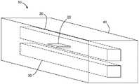
图1.根据本公开的实施例的波导的透视图。1. A perspective view of a waveguide according to an embodiment of the present disclosure.
图2.根据本公开的另一实施例的波导传感器的横截面视图。灰色区域是包层,白色区域是芯,以及标记有颜色的区域是掺杂有颜色染料的区域。顶部:沿着波导长度的截面视图(xz平面)。底部:跨越波导长度的截面视图(xy平面)。2. A cross-sectional view of a waveguide sensor according to another embodiment of the present disclosure. The grey area is the cladding, the white area is the core, and the area marked with color is the area doped with the color dye. Top: Cross-sectional view (xz plane) along the length of the waveguide. Bottom: Cross-sectional view (xy plane) across the length of the waveguide.
图3.可以用于所公开的波导的实施例中的示例性染料图案的顶视图(yz平面)。顶部:离散染料;中间:梯度染料;底部:离散和梯度染料的组合。Figure 3. Top view (yz plane) of an exemplary dye pattern that can be used in embodiments of the disclosed waveguide. Top: discrete dyes; middle: gradient dyes; bottom: combination of discrete and gradient dyes.
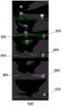
图4A.示出根据本公开的波导在按压变形期间的输出结果的一系列照片。4A. A series of photographs showing the output of a waveguide according to the present disclosure during compression deformation.
图4B.示出根据本公开的波导在拉伸变形期间的输出结果的一系列照片。Figure 4B. A series of photographs showing the output of a waveguide according to the present disclosure during tensile deformation.
图4C.示出根据本公开的波导在弯曲变形期间的输出结果的一系列照片。Figure 4C. A series of photographs showing the output of a waveguide according to the present disclosure during bending deformation.
图5.一种具有根据本公开的另一实施例的波导的传感器。Figure 5. A sensor with a waveguide according to another embodiment of the present disclosure.
具体实施方式Detailed ways
参考图1,在第一方面,本公开可以被实施为用于在传感器中使用的波导10。波导10包括具有第一折射率的第一芯20。第二芯30与第一芯20间隔开并与第一芯20平行,第二芯30具有第二折射率,第二折射率可以与第一折射率相同或不同。芯是透明的。在非限制性示例中,合适的芯透射80%或更多的具有400至750nm波长的入射可见光。根据本公开,其它合适的芯将是显而易见的。Referring to Figure 1, in a first aspect, the present disclosure may be implemented as a
芯可以具有各种横截面面积。例如,第一芯可以但不是必须大于第二芯。在示例中,第一芯宽3mm并且厚1.5mm,以及第二芯宽2mm并且厚1mm。The core can have various cross-sectional areas. For example, the first core may, but need not be, larger than the second core. In the example, the first core is 3 mm wide and 1.5 mm thick, and the second core is 2 mm wide and 1 mm thick.
包层40围绕第一芯20和第二芯30,包层40具有低于第一折射率和第二折射率的折射率。包层40的间隙部分42位于第一芯20和第二芯30之间。The
在一些实施例中,波导10的第一芯20包括被染色(即,掺杂有颜色染料)的第一区域22,在此有时将其称为第一染色区域22,第一染色区域22与包层40相邻并且沿着第一芯20的长度的一部分。在一些实施例中,第一染色区域22与包层40的间隙部分42相邻。在一些实施例中,第一染色区域22在第一芯20的小于或等于第一芯20的横截面面积的50%的横截面面积上延伸。在一些实施例中,与第一芯相邻的间隙部分的第一区域被染色。In some embodiments, the
通常,当前公开的波导操作使得波导在染色区域处的各种变形引起局部光行为的不同组合,选择性地包括由(一种或多种)染料引起的光颜色的变化、通过芯的几何形状的变化的光强度的损失以及芯之间的耦合。特别地,波导可以用于区分按压、拉伸和弯曲变形,和/或测量变形的位置和大小。In general, the presently disclosed waveguides operate such that various deformations of the waveguide at the dyed region induce different combinations of localized optical behavior, optionally including changes in light color caused by the dye(s), geometry through the core The varying light intensity loss as well as the coupling between the cores. In particular, waveguides can be used to differentiate compression, tension, and bending deformations, and/or measure the location and magnitude of deformations.
当不施加变形时,来自宽带光源(例如,白光LED)的光通过全内反射(TIR)以最小的损耗被引导到第一芯内部,这是因为波导芯和包层材料中的折射率(n)的差(例如,ncore~1.49、ncladding~1.4)。结果,在第一芯的另一端可以检测到明亮的白光,而在第二芯的一端可以检测到微弱的白光,由于薄的半透明硅酮阻挡层使得一些白光射线耦合到第二芯中。区分各种变形的方法总结在表1中,并在下面进行解释。When no deformation is applied, light from a broadband light source (eg, a white LED) is directed inside the first core by total internal reflection (TIR) with minimal loss due to the refractive indices in the waveguide core and cladding materials ( n) (eg, ncore ~1.49, ncladding ~1.4). As a result, bright white light can be detected at the other end of the first core, and weak white light can be detected at one end of the second core, some of the white light rays being coupled into the second core due to the thin translucent silicone barrier. The methods for distinguishing the various variants are summarized in Table 1 and explained below.
按压press
当波导被按压时,第一芯和第二芯之间的间隙包层被压缩,在按压力的位置处变薄并发生弯曲。这抑制了第一芯中的全内反射(TIR),引起局部漫反射。被漫反射的部分光线耦合到第二芯中,并通过TIR传播到第二芯的一端。当按压颜色区域时,第一芯中的白光射线将漫反射通过吸收染料并耦合到第二芯中。在波导的输出端,第一芯给予衰减的白光的输出,而第二芯给予色光的输出,其中颜色对应于被按压的染色区域,并且颜色饱和度指示所施加的力的强度。通过经由图案化吸收染料对空间信息进行颜色编码(图3和4A),可以实现对压力的分布式感测。When the waveguide is pressed, the gap cladding between the first core and the second core is compressed, thins and bends at the location of the pressing force. This suppresses total internal reflection (TIR) in the first core, causing local diffuse reflection. The diffusely reflected portion of the light is coupled into the second core and propagates to one end of the second core by TIR. When the color area is pressed, the white light rays in the first core will diffusely reflect through the absorbing dye and couple into the second core. At the output of the waveguide, the first core gives the output of attenuated white light and the second core gives the output of colored light, where the color corresponds to the pressed dyed area and the color saturation indicates the strength of the applied force. Distributed sensing of pressure can be achieved by color-coding spatial information via patterned absorbing dyes (Figures 3 and 4A).
拉伸stretch
波导也可以用于测量局部伸长。当染色区域被拉伸时,第一芯的光输出将从白光变成色光,其颜色对应于被拉伸的区域,并且颜色饱和度表示伸长的量。此效果与Beer-Lambert定律(A=ecL)一致,此定律规定通过介质传播的光(A)的衰减与衰减物质(e)的吸收率、衰减物质(c)的摩尔浓度和路径长度(L)成比例。在(一个或多个)染色区域,颜色吸收染料是主要的衰减物质。当染色区域被拉伸时,与未变形状态相比,染色区域(L)的长度增加,横截面面积减小,并且区域的体积不变。这是因为,例如聚氨酯的泊松比接近0.5,这意味着聚氨酯芯(在非限制性示例中)是不可压缩的。染料(c)的摩尔浓度在被拉伸的体积中不变。吸收率(e)是材料性质并且也不因变形而改变。因此,第一芯输出处的颜色变化仅仅是由于染色区域的长度增加。第二芯输出因为其也被拉伸而具有衰减强度的白光。Waveguides can also be used to measure local elongation. When the dyed area is stretched, the light output of the first core will change from white light to colored light, the color of which corresponds to the area being stretched, and the color saturation indicates the amount of stretch. This effect is consistent with the Beer-Lambert law (A=ecL), which specifies the attenuation of light (A) propagating through a medium versus the absorption rate of the attenuating species (e), the molar concentration of the attenuating species (c), and the path length (L ) is proportional. In the stained area(s), the color absorbing dye is the main attenuating substance. When the dyed region is stretched, the length of the dyed region (L) increases, the cross-sectional area decreases, and the volume of the region does not change compared to the undeformed state. This is because, for example, the Poisson's ratio of polyurethane is close to 0.5, which means that the polyurethane core (in a non-limiting example) is incompressible. The molar concentration of dye (c) does not change in the stretched volume. Absorptivity (e) is a material property and is also not changed by deformation. Therefore, the color change at the output of the first core is only due to the increased length of the dyed area. The second core outputs white light with attenuated intensity because it is also stretched.
弯曲bending
当波导局部弯曲远离染色表面时,第一芯输出将在颜色上从白色急剧改变为弯曲区域的颜色。这是因为在弯曲的位置处,第一芯中的射线功率集中在弯曲的外边缘,在外边缘处沉积颜色染料。在未变形的直波导中,射线功率集中在第一芯的中间,在第一芯的中间没有颜色染料而是透明的。第二芯输出因为其被放置在无色弯曲面(neutral bendingplane)附近而没有显著衰减的白光。When the waveguide is locally bent away from the dyed surface, the first core output will change sharply in color from white to the color of the bent region. This is because at the location of the bend, the ray power in the first core is concentrated at the outer edge of the bend, where the color dye is deposited. In an undeformed straight waveguide, the ray power is concentrated in the middle of the first core, which is transparent without color dyes. The second core outputs white light without significant attenuation because it is placed near the neutral bending plane.
通过读取和分析来自两个RGB传感器的强度信息和颜色信息,可以获得各种类型的变形的区别和测量。(表1)By reading and analyzing the intensity information and color information from the two RGB sensors, the distinction and measurement of various types of deformation can be obtained. (Table 1)

表1.波导中发生不同的变形时两个RGB传感器中的强度和RGB变化Table 1. Intensity and RGB changes in two RGB sensors with different deformations in the waveguide
可以使用各种染料。染料可以是例如可见光吸收染料、红外吸收染料等。染料可以是有机染料,有机染料可以包括吸收或散射颗粒。红外吸收染料可以包括散射红外光的颗粒。在示例中,染料是非散射染料,其可以具有未吸收波长(例如,未吸收的可见光)的期望的透射率(例如,90%或更大、95%或更大或99%或更大)。Various dyes can be used. The dyes may be, for example, visible light absorbing dyes, infrared absorbing dyes, and the like. The dyes can be organic dyes, which can include absorbing or scattering particles. Infrared absorbing dyes may include particles that scatter infrared light. In an example, the dye is a non-scattering dye, which can have a desired transmittance (eg, 90% or greater, 95% or greater, or 99% or greater) of unabsorbed wavelengths (eg, unabsorbed visible light).
例如,染料可以是具有可见光谱(例如,400-800nm)和/或红外光谱中的吸收波长的吸收染料。可以使用染料的各种组合。染料具有期望的透明度。在特定情况下,期望光穿过染色材料而不被散射。作为示例,光首先穿过染色区域(例如,蓝色染色区域)。染料的示例描述于本文中。在各种示例中,染料是无色透明的可见颜色吸收染料或此类染料的组合。在白光输入的情况下(例如,广谱白光LED),使用(一种或多种)染料来吸收广谱白光输入的各种波长。在示例中,染料吸收可见光谱中的一个或多个波长(例如,对于蓝色染料为550至680nm)。For example, the dye may be an absorbing dye having an absorption wavelength in the visible spectrum (eg, 400-800 nm) and/or the infrared spectrum. Various combinations of dyes can be used. The dye has the desired clarity. In certain cases, it is desirable for light to pass through the dyed material without being scattered. As an example, light first passes through a stained area (eg, a blue stained area). Examples of dyes are described herein. In various examples, the dye is a colorless transparent visible color absorbing dye or a combination of such dyes. In the case of a white light input (eg, a broad spectrum white light LED), dye(s) are used to absorb various wavelengths of the broad spectrum white light input. In an example, the dye absorbs one or more wavelengths in the visible spectrum (eg, 550 to 680 nm for blue dyes).
在染色区域内,对应的波长(例如,使用蓝色染料,550至680nm)被染料吸收。而未被吸收的波长继续透射到波导的一端。这对于不透明染料不起作用,不透明染料中所有光都被吸收、散射、反射或其组合,并且没有光透过它。In the dyed region, the corresponding wavelengths (eg, 550 to 680 nm with blue dyes) are absorbed by the dyes. The wavelengths that are not absorbed continue to be transmitted to one end of the waveguide. This does not work for opaque dyes, where all light is absorbed, scattered, reflected, or a combination thereof, and no light passes through it.
下表具有染料的示例的吸收/透射信息。“吸收的波长”是指染料吸收的波长(例如,蓝色染料通常将吸收550-700nm(吸收的波长)的波长,以及透射400-550nm(未吸收的波长)的波长。The table below has absorption/transmission information for examples of dyes. "Absorbed wavelength" refers to the wavelengths that the dye absorbs (eg, a blue dye will typically absorb wavelengths from 550-700 nm (the absorbed wavelength), and transmit wavelengths from 400-550 nm (the unabsorbed wavelength).
如上所述,颜色染料可以放置于第一芯中,或者可以放置于两个芯之间的包层中。对于后一种布置,可以感测弯曲和按压变形的位置和大小,但是将丢失拉伸变形的位置信息。As mentioned above, the color dye can be placed in the first core, or it can be placed in the cladding between the two cores. For the latter arrangement, the position and magnitude of the bending and pressing deformations can be sensed, but the positional information of the stretching deformations will be lost.
染料图案Dye Pattern
在一些实施例中,第一芯可具有一个或多个额外的染色区域。在一些实施例中,第一染色区域和一个或多个额外的染色区域沿着第一芯的纵向长度不彼此重叠。这样,染料区可以被认为是离散的(参见例如图3的顶部,并且在下文进一步描述)。在一些实施例中,第一染色区域沿着第一芯的长度与额外的染色区域重叠。例如,第一染色区域和重叠的额外的染色区域可以是锥形的以沿着第一芯的长度形成颜色梯度(参见例如图3的中间部分,并且下文进一步描述)。In some embodiments, the first core may have one or more additional dyed regions. In some embodiments, the first dyed region and the one or more additional dyed regions do not overlap each other along the longitudinal length of the first core. As such, the dye regions can be considered discrete (see, eg, the top of Figure 3, and described further below). In some embodiments, the first dyed region overlaps with additional dyed regions along the length of the first core. For example, the first dyed region and the overlapping additional dyed regions may be tapered to form a color gradient along the length of the first core (see, eg, the middle portion of Figure 3, and described further below).
通过使用具有不同的颜色图案设计的一个或多个芯,可以实现各种感测能力。图案设计包括但不限于离散染料掺杂、梯度染料掺杂和两者的组合。示例性的染料图案示出在图3中并描述如下。Various sensing capabilities can be achieved by using one or more cores with different color pattern designs. Pattern designs include, but are not limited to, discrete dye doping, gradient dye doping, and combinations of the two. Exemplary dye patterns are shown in Figure 3 and described below.
染料图案可以是离散染料图案。在离散染料设计的示例中(例如,图3,顶部的设计),在第一芯的顶表面上的矩形腔中沉积染料薄层。空间分辨率取决于染料的长度和染料之间的间隔。因此,此设计提供了对按压、拉伸和弯曲的离散感测。尽管空间分辨率有限,但此设计提供了多位置变形感测的能力。例如,在多触摸触觉感测的情况下,此设计可以通过在第二芯中插入输出颜色来测量施加到每个染色区域的力。The dye pattern may be a discrete dye pattern. In an example of a discrete dye design (eg, Figure 3, design at the top), a thin layer of dye is deposited in a rectangular cavity on the top surface of the first core. Spatial resolution depends on the length of the dye and the spacing between the dyes. Therefore, this design provides discrete sensing of compression, stretching and bending. Despite the limited spatial resolution, this design provides the capability for multi-position deformation sensing. For example, in the case of multi-touch tactile sensing, this design can measure the force applied to each dyed area by inserting the output color in the second core.
染料图案可以是梯度染料图案。梯度染料设计(例如,图3,中间部分的设计)解决了离散染料设计中的空间分辨率限制。通过在重叠的互补三角形腔中掺杂两种颜色染料的薄层,创建颜色光谱梯度。在图3的中间图案所示的示例中,颜色的光谱沿着染色区域的长度从粉色(左)连续地变化到绿色(右)。由于波导中白光的射线功率关于xz平面(由图3中的黑色虚线表示)对称,因此在沿着波导长度(z方向)变形时的颜色变化对应于由染料限定的颜色梯度。因此,实现了针对各种变形的连续空间分辨率。The dye pattern may be a gradient dye pattern. Gradient dye designs (eg, Figure 3, design in the middle) address the spatial resolution limitations in discrete dye designs. Color spectral gradients are created by doping thin layers of two color dyes in overlapping complementary triangular cavities. In the example shown in the middle pattern of Figure 3, the spectrum of colors varies continuously from pink (left) to green (right) along the length of the stained region. Since the ray power of white light in the waveguide is symmetric about the xz plane (represented by the black dashed line in Figure 3), the color change upon deformation along the waveguide length (z-direction) corresponds to the color gradient defined by the dye. Thus, continuous spatial resolution for various deformations is achieved.
利用上述两种图案的优点,其中每个离散区域被细分为两种颜色以形成颜色梯度的组合图案(例如,图3,底部的设计)可以用于检测多位置变形并且在每个染色区域中具有分布感测能力。Taking advantage of the two patterns described above, where each discrete region is subdivided into two colors to form a combined pattern of color gradients (eg, Figure 3, design at the bottom) can be used to detect multi-position deformations and in each dyed region It has distributed sensing capability.
包层40可以是完全或部分不透明的。例如,包层可以具有大于10dB/cm的吸收率。在一些实施例中,包层可以被配置为吸收光。The
第一芯20和第二芯30可以具有各种尺寸和/或形状。例如,第一芯20和/或第二芯30可以具有圆形、多边形等的横截面形状。只要将间隙包层夹在中间的两个面(例如,第一芯的染色面和第二芯的相邻面)是平行面,就可以使用任何形状/尺寸变型。例如,第一芯和第二芯可以是两个半球等。第一芯20可以具有大于第二芯30的横截面面积的横截面面积,在其它实施例中,第一芯和第二芯可以具有相等的横截面面积。在其它实施例中,第一芯20可以具有小于第二芯30的横截面面积的横截面面积,芯可以针对特别的应用的需要而是大的或小的。例如,第一芯20和/或第二芯30可以具有10μm至5cm的直径,包括所有整数μm值和其间的范围在内。在另一示例中,第一芯20和/或第二芯30的横截面面积可以是100μm2至25cm2,包括所有整数μm2的值及其间的范围在内。The
芯和包层可以包括各种弹性材料。合适的弹性材料的非限制性示例包括各种合成橡胶(例如,硅橡胶、聚氨酯、苯乙烯-丁二烯橡胶、聚丁二烯、氯丁橡胶等)、天然胶乳橡胶、可生物降解材料(例如,聚癸二酸)或它们的组合。各种官能团(例如,烯烃、羧基、苯、丙烯酰基等)可以接枝到这些材料的主链上以改变芯和包层两者的光学性质(例如,折射率、吸光度)。每个芯可包括相同的材料或不同的材料。在一些实施例中,第一芯和第二芯由硬度比包层的材料高的材料制成。The core and cladding can include various elastic materials. Non-limiting examples of suitable elastic materials include various synthetic rubbers (eg, silicone rubber, polyurethane, styrene-butadiene rubber, polybutadiene, neoprene, etc.), natural latex rubber, biodegradable materials ( For example, polysebacic acid) or a combination thereof. Various functional groups (eg, olefin, carboxyl, benzene, acryl, etc.) can be grafted onto the backbone of these materials to alter the optical properties (eg, refractive index, absorbance) of both the core and cladding. Each core may comprise the same material or a different material. In some embodiments, the first core and the second core are made of a material that is harder than the material of the cladding.
在一些实施例中,波导500可以具有包层540、第一芯520、第二芯530和第三芯550。第二芯530和第三芯550中的每一个与第一芯520相邻。包层540的第二间隙部分544位于第三芯550和第一芯520之间。第一芯520的与第二间隙包层544相邻的第二区域526被染色。图5示出一种配置的示例,在此示例中,波导包括放置于中间的主芯(第一芯)和各自与第一芯相邻放置的两个第二芯。第一芯的一侧掺杂有离散的染料图案,而其相对侧掺杂有梯度染料图案。通过使用例如RGB传感器检测三个芯的输出,此配置允许同时进行由离散染料使能的多位置感测和由梯度染料使能的连续感测。In some embodiments, the
参考图2,在另一方面,本公开可以被实施为传感器100。传感器100包括根据本文所述的实施例中的任一个的波导110。例如,传感器100可以包括具有第一芯120、第二芯130和包层140的波导110。第一芯的第一染色区域122与包层140的间隙部分相邻。Referring to FIG. 2 , in another aspect, the present disclosure may be implemented as a
传感器100还包括耦合到第一芯120的输入端124的宽带光源170。示例性光源可以是发光二极管(LED)。诸如白光LED的广谱光源将与波导的染色区域协作,以提供用于本文所述目的合适的输出信号。应当注意的是,示例提供有“颜色”染料和“颜色”检测器,并且这样的实施例旨在包括对于人类不可见的波长,诸如红外光。光源的非限制性示例包括可见光源、红外光源等或它们的组合。The
第一检测器180耦合到第一芯120的输出端126。输出端126可以在第一芯120的与输入端124相对的一端处。在其它实施例中,输入端和输出端可以在第一芯的同一物理端,并且反射器或类似设备可以用在芯的相对端。第二检测器182耦合到第二芯130的输出端136。检测器的非限制性示例包括可见光传感器(包括例如RGB传感器)、红外传感器等或其组合。The
这种传感器的实施例可以被称为基于光波导的分布式传感器、光转换器系统或波导传感器/系统。通过由弹性材料制成并结合有可见光谱吸收染料,传感器可以测量和区分变形的各种模式的大小和位置:按压、拉伸、弯曲或其组合。在各种示例中,所公开的传感器的特征在于紧凑、低成本、易于制造的系统,该系统包括如上所述的波导,加上从传感器的一个端用作光源的宽谱发光二极管(LED)和从另一个端接收转换的光学信号的便携式红-绿-蓝(RGB)色光传感器芯片。Embodiments of such sensors may be referred to as optical waveguide based distributed sensors, optical converter systems or waveguide sensors/systems. By being made of an elastic material and incorporating visible-spectrum absorbing dyes, the sensor can measure and differentiate the magnitude and location of various modes of deformation: pressing, stretching, bending, or a combination thereof. In various examples, the disclosed sensor features a compact, low-cost, easy-to-manufacture system comprising a waveguide as described above, plus a broad spectrum light emitting diode (LED) used as a light source from one end of the sensor and a portable red-green-blue (RGB) color light sensor chip that receives the converted optical signal from the other end.
可以可期望的是,芯的横截面尺寸与检测器尺寸(例如RGB芯片的尺寸)相当。在一些示例中,可以可期望的是,芯的横截面面积不小于传感器的主动感测面积(例如,可以具有例如400平方微米的有效感测面积的RGB芯片)。It may be desirable for the cross-sectional dimensions of the core to be comparable to the detector dimensions (eg, the dimensions of an RGB chip). In some examples, it may be desirable that the cross-sectional area of the core is not less than the active sensing area of the sensor (eg, an RGB chip that may have an effective sensing area of, eg, 400 square microns).
在另一方面,本公开可以被实施为一种检测波导的变形的方法。方法包括提供根据本文公开的实施例中的任一个的传感器。方法还包括检测第一芯的输出端和第二芯的输出端处的光变化。基于检测到的光变化区分和/或测量波导的变形。光变化可以包括例如光强度的变化和/或波长的变化(即RGB变化)。这种变化可以在第一芯、第二芯或这两个芯内。In another aspect, the present disclosure can be implemented as a method of detecting deformation of a waveguide. The method includes providing a sensor according to any of the embodiments disclosed herein. The method also includes detecting light changes at the output of the first core and the output of the second core. The deformation of the waveguide is differentiated and/or measured based on the detected light changes. Light changes may include, for example, changes in light intensity and/or changes in wavelength (ie, RGB changes). This variation can be within the first core, the second core, or both.
本公开在各种示例中描述了多芯、掺杂颜色(染色)的可拉伸波导,它可以被设计为紧凑且低成本的光波导传感器。传感器可以区分按压、拉伸和弯曲变形,并测量变形的位置和大小。在一些实施例中,传感器由弹性材料(例如,软弹性材料)制成。这样,传感器可以有利地与各种机器人致动器(例如,软机器人致动器)一起使用。通过创新的设计和集成的电子器件,传感器可以提供同时的分布式感测并且解耦变形的多个模式,具有例如低至亚毫米和宽范围的空间灵敏度。The present disclosure describes, in various examples, multi-core, color-doped (dyed) stretchable waveguides that can be designed as compact and low-cost optical waveguide sensors. The sensors can differentiate between compression, stretch and bending deformations and measure the location and magnitude of the deformations. In some embodiments, the sensor is made of an elastic material (eg, a soft elastic material). In this way, the sensor can be advantageously used with various robotic actuators (eg, soft robotic actuators). Through innovative design and integrated electronics, sensors can provide simultaneous distributed sensing and decouple multiple modes of deformation, with, for example, low to sub-millimeter and wide-range spatial sensitivities.
本公开的波导和传感器的实施例提供各种能力,包括例如可以使用简单设置、容易的无线连接或其组合来检测和区分局部压力、曲率和伸长的触觉传感器。使用传感器测量/获得的数据在诸如远程手术中的实时感测、虚拟现实(VR)手套、软假体和矫形器以及智能机器人手和臂等应用中提供期望的信息。Embodiments of waveguides and sensors of the present disclosure provide various capabilities, including, for example, tactile sensors that can detect and differentiate localized pressure, curvature, and elongation using simple setup, easy wireless connectivity, or a combination thereof. Data measured/obtained using sensors provides desired information in applications such as real-time sensing in telesurgery, virtual reality (VR) gloves, soft prostheses and orthoses, and intelligent robotic hands and arms.
在各种示例中,本公开的传感器可以提供以下中的一个或多个:In various examples, the sensors of the present disclosure may provide one or more of the following:
·传感器可以分别区分和测量各种变形的大小和分布位置,包括按压、拉伸、弯曲及其组合。Sensors can distinguish and measure the magnitude and distribution of various deformations, including compression, stretching, bending, and combinations thereof, respectively.
·波导仅由软性、柔性和高度可拉伸的弹性体制成,弹性体可以拉伸高达600%的单轴应变。这使得传感器适应和适合于可以大幅变形的复杂形状的表面或物体。Waveguides are made only of soft, flexible and highly stretchable elastomers that can stretch up to 600% uniaxial strain. This allows the sensor to adapt and adapt to complex shaped surfaces or objects that can deform substantially.
·通过经由在波导的芯中以顺序/图案掺杂的可见吸收染料而选择性吸收白光来实现沿着一个或多个波导的分布式感测。• Distributed sensing along one or more waveguides by selectively absorbing white light via visible absorbing dyes doped in sequence/patterns in the core of the waveguide.
·传感器比相关技术更紧凑,更易于实现,成本更低,并且消耗更少的功率。· Sensors are more compact, easier to implement, cost less, and consume less power than related technologies.
·变形的模式、位置和大小可以直接从由RGB传感器收集的总光强度、RGB值和饱和度的数据测量和转换。与相关技术相比,数据不需要进一步的复杂数据解释。The mode, location and magnitude of the deformation can be measured and converted directly from the data collected by the RGB sensor for total light intensity, RGB value and saturation. In contrast to related techniques, the data do not require further complex data interpretation.
·通过更改波导中不同层的厚度,传感器的范围和灵敏度可以被调整到不同的应用。• By changing the thickness of different layers in the waveguide, the range and sensitivity of the sensor can be tuned to different applications.
传感器可以检测或感测变形(例如,变形模式、变形的位置、大小或其组合)。传感器可以检测各种变形模式(例如,按压、拉伸、弯曲或其组合)。The sensor may detect or sense deformation (eg, deformation pattern, deformation location, magnitude, or a combination thereof). The sensors can detect various deformation modes (eg, pressing, stretching, bending, or a combination thereof).
波导传感器包括至少一个芯,该芯具有一个或多个被染色(例如,染有颜色)的区域(例如,与间隙包层相邻)。例如,使用一个或多个染料,染料可以是离散或梯度图案。染料使用例如(一种或多种)颜色对空间信息进行编码。(一个或多个)染色区域被配置在波导中,使得在(一个或多个)变形时,波导输出颜色变化,从而提供空间信息和变形模式。The waveguide sensor includes at least one core having one or more regions that are colored (eg, colored) (eg, adjacent to the interstitial cladding). For example, using one or more dyes, the dyes may be in discrete or gradient patterns. Dyes encode spatial information using, for example, color(s). The dyed region(s) are configured in the waveguide such that upon deformation of the waveguide(s) the waveguide output color changes, thereby providing spatial information and deformation modes.
示例性实施例的制造Manufacture of Exemplary Embodiments
在一个示例性(即非限制性实施例)中,波导包括弹性体包层(例如硅酮弹性体包层),围绕两个或多个透明弹性体芯(例如透明聚氨酯(PU)弹性体芯)。芯(例如第一芯和第二芯)可以具有各种配置。例如,两个芯放置为一个在另一个之上,由透明或半透明包层(例如硅酮层)的共用薄层分离。In one exemplary (ie, non-limiting) embodiment, the waveguide includes an elastomeric cladding (eg, a silicone elastomeric cladding) surrounding two or more transparent elastomeric cores (eg, a transparent polyurethane (PU) elastomeric core) ). The cores (eg, the first core and the second core) can have various configurations. For example, two cores are placed one on top of the other, separated by a common thin layer of transparent or translucent cladding (eg, a silicone layer).
例如,可以使用硅酮模具通过复制模塑透明弹性体(例如,PU弹性体,诸如,ClearFlex30,SMOOTH-ON)来制造芯,通过在3D打印的刚性模具上浇铸刚性硅酮弹性体(例如,ELASTOSIL M4601,Wacker Chemie AG)制备硅酮模具。For example, cores can be fabricated using silicone molds by replica molding transparent elastomers (eg, PU elastomers such as ClearFlex30, SMOOTH-ON) by casting rigid silicone elastomers (eg, 3D printed rigid molds) on top of 3D printed rigid molds. ELASTOSIL M4601, Wacker Chemie AG) made silicone molds.
例如,通过使用硅酮模具复制模塑透明PU弹性体(Clear Flex30,SMOOTH-ON)来制造第一芯(例如,第一芯诸如,例如PU芯),硅酮模具通过在3D打印的刚性模具上浇铸刚性硅酮弹性体(ELASTOSIL M4601,Wacker Chemie AG)制备。然后腔被图案化在固化的第一芯中,随后用掺杂有一种或多种可见颜色吸收染料(例如,无色透明的可见颜色吸收染料,诸如例如,EP7701,可从Eager Polymers获得)的透明弹性体(例如,Clear Flex30)填充并固化腔。第二芯(例如PU芯)使用透明弹性体(例如,Clear Flex30)使用与上述第一芯相同的方法制造,但没有腔或颜色吸收染料。For example, a first core (eg, a first core such as, for example, a PU core) is fabricated by replica molding a transparent PU elastomer (Clear Flex30, SMOOTH-ON) using a silicone mold through a rigid mold 3D printed Prepared by cast-on-rigid silicone elastomer (ELASTOSIL M4601, Wacker Chemie AG). The cavities are then patterned in the cured first core, followed by cavities doped with one or more visible color absorbing dyes (eg, a colorless transparent visible color absorbing dye such as, for example, EP7701, available from Eager Polymers). A clear elastomer (eg, Clear Flex30) fills and cures the cavity. The second core (eg, PU core) is fabricated using a clear elastomer (eg, Clear Flex30) using the same method as the first core described above, but without the cavity or color absorbing dye.
例如,使用3D打印塑料模具复制模塑具有腔的波导的弹性体包层(例如,硅酮包层,诸如例如Dragon Skin 20SMOOTH-ON)。第一芯(例如“底部”或“下部”芯诸如,例如底部PU芯)被转移到弹性体包层的腔中,其中图案化的颜色区域面向上。半透明弹性体(诸如,例如半透明硅酮(例如Dragon Skin20,SMOOTH-ON))的薄层或透明硅酮(例如SYLGARD184,DOWCORNING)的薄层沉积在PU的颜色表面上。第二芯(例如“顶部”或“上部”PU芯)被转移到薄硅酮层上。然后,在第二芯上沉积弹性体包层(例如,硅酮包层诸如,例如Dragon Skin20SMOOTH-ON)的顶层,以完成波导包层。使设备完成固化(例如在室温下4小时)。For example, an elastomeric cladding (eg, a silicone cladding, such as, for example, Dragon Skin 20SMOOTH-ON) of a waveguide with a cavity is replica-molded using a 3D printed plastic mold. A first core (eg, a "bottom" or "lower" core such as, for example, a bottom PU core) is transferred into the cavity of the elastomeric cladding with the patterned color areas facing up. Thin layers of translucent elastomers such as, for example, translucent silicones (
虽然在前述示例中描述了复制模塑,但是传感器的制造(例如,芯形成和包层形成)也可以使用3D打印来执行,3D打印包括直接墨水书写(Direct Ink Writing)和立体光刻。Although replication molding is described in the foregoing examples, fabrication of sensors (eg, core formation and cladding formation) can also be performed using 3D printing, including Direct Ink Writing and stereolithography.
在波导的输入端处,诸如白光LED芯片(Cree Inc.XQEAWT-H2-0000-00000BEE5)的广谱光源被耦合到第一芯并与第一芯对准。在波导的输出端处,诸如RGB传感器芯片(TCS3472,TAOS)的检测器被附接到第一芯并与第一芯对准,以及另一检测器被附接到第二芯并与第二芯对准(见图2)。可以使用各种光源和检测器。光源的非限制性示例包括可见光源、红外光源等或它们的组合。检测器的非限制性示例包括可见光传感器(包括RGB传感器)、红外传感器等或它们的组合。At the input end of the waveguide, a broad spectrum light source such as a white light LED chip (Cree Inc. XQEAWT-H2-0000-00000BEE5) is coupled to and aligned with the first core. At the output of the waveguide, a detector such as an RGB sensor chip (TCS3472, TAOS) is attached to and aligned with the first core, and another detector is attached to and aligned with the second core core alignment (see Figure 2). Various light sources and detectors can be used. Non-limiting examples of light sources include visible light sources, infrared light sources, and the like, or combinations thereof. Non-limiting examples of detectors include visible light sensors (including RGB sensors), infrared sensors, and the like, or combinations thereof.
进一步描述further description
间隙包层可以被认为是部分遮光层。例如,间隙包层位于两个芯之间,例如第一芯和第二芯之间,使得当一个芯(例如第二芯)被按压时,间隙包层变薄并且变形,足以使光从另一个芯进入一个芯(例如,从第一芯进入第二芯)。间隙包层的厚度(例如,表示为tic)可以取决于两个芯(例如,第一芯和第二芯)的厚度,以及对于压力的灵敏度和范围的要求。随着tic变薄,按压力灵敏度将增加(更灵敏)。随着tic变厚,传感器将能够感测较大的按压力。tic是用于不同应用的可调参数,并且可以跨越宽范围的厚度。例如,使用典型的芯尺寸(例如,本文所述的芯尺寸),tic的大致范围可以大于0mm且小于2mm。The gap cladding can be considered as a partial light shielding layer. For example, an interstitial cladding is located between two cores, eg, a first core and a second core, such that when one core (eg, a second core) is pressed, the interstitial cladding thins and deforms enough to allow light to escape from the other A core enters a core (eg, from a first core into a second core). The thickness of the interstitial cladding (eg, denotedtic ) may depend on the thickness of the two cores (eg, the first core and the second core), as well as the sensitivity and range requirements for pressure. As thetic gets thinner, the compression force sensitivity will increase (more sensitive). As thetic gets thicker, the sensor will be able to sense greater pressing force.tic is an adjustable parameter for different applications and can span a wide range of thicknesses. For example, using typical core sizes (eg, those described herein), the approximate range oftic may be greater than 0 mm and less than 2 mm.
本发明利用一种或多种染料(例如吸收染料)的应用来实现各种变形的区分与分布式感测的低成本、紧凑布置的目标。本文描述了包层、芯和染料的各种布置。(一种或多种)波导的可替换实施例包括以下中的一个或多个:The present invention utilizes the application of one or more dyes (eg, absorbing dyes) to achieve the goal of low-cost, compact arrangements for differentiation of various variants and distributed sensing. Various arrangements of cladding, core and dye are described herein. Alternative embodiments of the waveguide(s) include one or more of the following:
·不同放置的染料。例如,染料可以掺杂在硅酮包层中而不是PU芯中,或者染料可以放置在多个平面中以检测不同方向上的变形。· Different placement of dyes. For example, dyes can be doped in the silicone cladding instead of the PU core, or the dyes can be placed in multiple planes to detect deformations in different directions.
·不同形状的芯和包层,而不是直矩形。· Different shapes of core and cladding instead of straight rectangles.
·不同数量的芯。· Different numbers of cores.
·不同放置的芯和包层。• Differently placed core and cladding.
·不同长度的传感器。· Sensors of different lengths.
·用于制造芯和包层的不同现成材料。• Different off-the-shelf materials for making core and cladding.
·不同放置的刚性光电子组件:LED和RGB传感器。由于波导的一个端涂有反射涂层,LED和RGB传感器可以被布置在波导的相同端,使得整个传感器设计更紧凑。Rigid optoelectronic components in different placements: LEDs and RGB sensors. Since one end of the waveguide is coated with a reflective coating, the LED and RGB sensor can be arranged on the same end of the waveguide, making the overall sensor design more compact.
传感器(可以被称为波导传感器)可以单独使用,即,单独使用一个波导,以感测诸如按压、弯曲、拉伸或其组合的变形,并且在2D空间中重建形状。在另一配置中,通过并排地布置和/或在不同层中布置多个波导,可以构造2D分布式感测平面用于3D空间中的实时感测和形状重建。A sensor (which may be referred to as a waveguide sensor) can be used alone, ie, a waveguide alone, to sense deformations such as compression, bending, stretching, or a combination thereof, and reconstruct the shape in 2D space. In another configuration, by arranging multiple waveguides side-by-side and/or in different layers, a 2D distributed sensing plane can be constructed for real-time sensing and shape reconstruction in 3D space.
基于用于在广泛应用中进行感测和形状重建的布置(例如,如本文所述),波导传感器或多个波导传感器可以被集成到软机器或机器人中,广泛应用包括例如远程手术、VR手套、软矫正器/假体、机器人手/臂等。Based on arrangements for sensing and shape reconstruction in a wide range of applications (eg, as described herein), a waveguide sensor or multiple waveguide sensors can be integrated into soft machines or robots, including, for example, telesurgery, VR gloves , soft orthosis/prosthesis, robotic hand/arm, etc.
在示例中,软机器或机器人包括本公开的一个或多个波导传感器。在软机器或机器人包括多个波导传感器的情况下,传感器可以全部是相同的传感器配置或至少两个不同传感器配置的组合。In an example, a soft machine or robot includes one or more waveguide sensors of the present disclosure. Where the soft machine or robot includes multiple waveguide sensors, the sensors may all be the same sensor configuration or a combination of at least two different sensor configurations.
在本文公开的各种实施例和示例中描述的方法的步骤足以实施本发明的方法。因此,在实施例中,方法基本上由本文公开的方法的步骤的组合组成。在另一实施例中,方法由这些步骤组成。在另一实施例中方法包括这些步骤。The steps of the methods described in the various embodiments and examples disclosed herein are sufficient to implement the methods of the present invention. Thus, in an embodiment, a method consists essentially of a combination of the steps of the methods disclosed herein. In another embodiment, the method consists of these steps. In another embodiment the method includes these steps.
以下,描述本公开的各种示例:Below, various examples of the present disclosure are described:
示例1.一种波导,包括具有第一折射率的第一芯;具有第二折射率的第二芯,第二芯与第一芯间隔开并与第一芯平行;围绕第一芯和第二芯的包层,包层具有低于第一折射率和第二折射率的折射率,以及其中包层的间隙部分位于第一芯和第二芯之间;以及其中第一芯的与包层相邻的第一区域或者包层的与第一芯相邻的第一区域被染色。Example 1. A waveguide comprising a first core having a first index of refraction; a second core having a second index of refraction, the second core being spaced apart from and parallel to the first core; surrounding the first core and the second core A cladding of two cores, the cladding having a refractive index lower than the first and second refractive indices, and wherein a gap portion of the cladding is located between the first core and the second core; and wherein the first core and the cladding The first region adjacent to the layer or the first region of the cladding adjacent to the first core is dyed.
示例2.如示例1所述的波导,其中第一染色区域是第一芯的并且与间隙包层相邻。Example 2. The waveguide of example 1, wherein the first dyed region is of the first core and adjacent to the interstitial cladding.
示例3.如前述示例中的任一个所述的波导,其中第一染色区域在小于或等于第一芯的横截面面积的50%的第一芯的横截面面积上延伸。Example 3. The waveguide of any of the preceding examples, wherein the first dyed region extends over a cross-sectional area of the first core that is less than or equal to 50% of the cross-sectional area of the first core.
示例4.如前述示例中的任一个所述的波导,其中包层包括硅酮。Example 4. The waveguide of any of the preceding examples, wherein the cladding comprises silicone.
示例5.如前述示例中的任一个所述的波导,其中第一芯和/或第二芯包括聚氨酯。Example 5. The waveguide of any of the preceding examples, wherein the first core and/or the second core comprise polyurethane.
示例6.如前述示例中的任一个所述的波导,其中第一芯的横截面面积大于第二芯的横截面面积。Example 6. The waveguide of any of the preceding examples, wherein the cross-sectional area of the first core is greater than the cross-sectional area of the second core.
示例7.如前述示例中的任一个所述的波导,其中第一折射率与第二折射率相同。Example 7. The waveguide of any of the preceding examples, wherein the first index of refraction is the same as the second index of refraction.
示例8.如前述示例中的任一个所述的波导,其中第一芯具有包括所有整数μm值和其间的范围在内的10μm至5cm的直径,和/或包括所有整数μm2值和其间的范围在内的100μm2至25cm2的横截面面积。Example 8. The waveguide of any of the preceding examples, wherein the first core has a diameter of 10 μm to5 cm inclusive of all integer μm values and ranges therebetween, and/or inclusive of all integer μm values and ranges therebetween Cross-sectional area in the range of 100 μm2 to 25 cm2 .
示例9.如前述示例中的任一个所述的波导,其中所述第二芯具有包括所有整数μm值和其间的范围在内的10μm至5cm的直径,和/或包括所有整数μm2值和其间的范围在内的100μm2至25cm2的横截面面积。Example 9. The waveguide of any of the preceding examples, wherein the second core has a diameter of 10 μm to5 cm inclusive of all integer μm values and ranges therebetween, and/or inclusive of all integer μm values and A cross-sectional area in the range of 100 μm2 to 25 cm2 .
示例10.如前述示例中的任一个所述的波导,其中第一芯具有圆形、多边形等的横截面形状。Example 10. The waveguide of any of the preceding examples, wherein the first core has a circular, polygonal, etc. cross-sectional shape.
示例11.如前述示例中的任一个所述的波导,其中第二芯具有圆形、多边形等的横截面形状。Example 11. The waveguide of any of the preceding examples, wherein the second core has a circular, polygonal, etc. cross-sectional shape.
示例12.如前述示例中的任一个所述的波导,其中第一芯和第二芯由硬度比包层的材料高的材料制成。Example 12. The waveguide of any of the preceding examples, wherein the first core and the second core are made of a material that is harder than the material of the cladding.
示例13.如前述示例中的任一个所述的波导,其中所第一芯具有一个或多个额外的染色区域。Example 13. The waveguide of any of the preceding examples, wherein the first core has one or more additional dyed regions.
示例14.如示例13所述的波导,其中第一染色区域和/或一个或多个额外的染色区域沿着第一芯的纵向长度不彼此重叠。Example 14. The waveguide of Example 13, wherein the first dyed region and/or the one or more additional dyed regions do not overlap each other along the longitudinal length of the first core.
示例15.如示例13所述的波导,其中第一染色区域沿着第一芯的长度与额外的染色区域重叠。Example 15. The waveguide of Example 13, wherein the first dyed region overlaps the additional dyed region along the length of the first core.
示例16.如示例15所述的波导,其中重叠的第一染色区域和额外的染色区域是锥形的,以沿着第一芯的长度形成颜色梯度。Example 16. The waveguide of Example 15, wherein the overlapping first dyed region and the additional dyed region are tapered to form a color gradient along the length of the first core.
示例17.如前述示例中的任一个所述的波导,还包括与第一芯相邻的第三芯,以及位于第三芯和第一芯之间的第二间隙包层;以及其中第一芯的与第二间隙包层相邻的第二区域被染色。Example 17. The waveguide of any of the preceding examples, further comprising a third core adjacent to the first core, and a second interstitial cladding located between the third core and the first core; and wherein the first A second region of the core adjacent to the second interstitial cladding is dyed.
示例18.一种传感器,包括如前述示例中任一个所述的波导;耦合到第一芯的输入端的广谱光源;耦合到第一芯的输出端的第一检测器;以及耦合到第二芯的输出端的第二检测器。Example 18. A sensor comprising the waveguide of any of the preceding examples; a broad-spectrum light source coupled to an input of a first core; a first detector coupled to an output of the first core; and coupled to a second core the output of the second detector.
示例19.如示例18所述的传感器,还包括与第一检测器和第二检测器电子通信的控制器,控制器被配置为基于在第一检测器和/或第二检测器处接收的光确定外力的位置和/或大小。Example 19. The sensor of Example 18, further comprising a controller in electronic communication with the first detector and the second detector, the controller configured to Light determines the location and/or magnitude of the external force.
示例20.如示例18-19中的任一个所述的传感器,其中第一芯的输入端在第一芯的与输入端相对的一端处。Example 20. The sensor of any of examples 18-19, wherein the input of the first core is at an end of the first core opposite the input.
示例21.一种检测波导的变形的方法,包括提供如示例18-20中的任一个所述的传感器;检测第一芯的输出端和第二芯的输出端处的光变化;以及基于检测到的光变化区分和/或测量波导的变形。Example 21. A method of detecting deformation of a waveguide, comprising providing the sensor of any of Examples 18-20; detecting changes in light at an output of a first core and an output of a second core; and based on detecting The resulting light changes differentiate and/or measure the deformation of the waveguide.
示例22.如示例21所述的方法,其中光变化包括光强度变化和RGB变化。Example 22. The method of Example 21, wherein the light changes include light intensity changes and RGB changes.
尽管已经关于一个或多个特定实施例描述了本公开,但是将理解的是,可以在不脱离本公开的精神和范围的情况下做出本公开的其它实施例。Although the present disclosure has been described with respect to one or more specific embodiments, it will be understood that other embodiments of the present disclosure can be made without departing from the spirit and scope of the present disclosure.
Claims (22)
Applications Claiming Priority (5)
| Application Number | Priority Date | Filing Date | Title |
|---|---|---|---|
| US201762592073P | 2017-11-29 | 2017-11-29 | |
| US62/592,073 | 2017-11-29 | ||
| US201862642407P | 2018-03-13 | 2018-03-13 | |
| US62/642,407 | 2018-03-13 | ||
| PCT/US2018/063173WO2019108862A1 (en) | 2017-11-29 | 2018-11-29 | Waveguide and sensor based on same |
Publications (1)
| Publication Number | Publication Date |
|---|---|
| CN111656235Atrue CN111656235A (en) | 2020-09-11 |
Family
ID=66664252
Family Applications (2)
| Application Number | Title | Priority Date | Filing Date |
|---|---|---|---|
| CN201880087583.2APendingCN111656235A (en) | 2017-11-29 | 2018-11-29 | Waveguides and Waveguide-Based Sensors |
| CN201880088089.8AActiveCN111656308B (en) | 2017-11-29 | 2018-11-29 | Elastic light guide coupling for one-, two-and three-dimensional continuous position location |
Family Applications After (1)
| Application Number | Title | Priority Date | Filing Date |
|---|---|---|---|
| CN201880088089.8AActiveCN111656308B (en) | 2017-11-29 | 2018-11-29 | Elastic light guide coupling for one-, two-and three-dimensional continuous position location |
Country Status (5)
| Country | Link |
|---|---|
| US (3) | US11614583B2 (en) |
| EP (2) | EP3717993A4 (en) |
| CN (2) | CN111656235A (en) |
| FI (1) | FI3717944T3 (en) |
| WO (2) | WO2019108861A1 (en) |
Cited By (2)
| Publication number | Priority date | Publication date | Assignee | Title |
|---|---|---|---|---|
| CN113790670A (en)* | 2021-08-26 | 2021-12-14 | 上海理工大学 | A kind of flexible distributed optical fiber sensor and manufacturing method |
| CN119043541A (en)* | 2024-10-30 | 2024-11-29 | 吉林大学 | Fingertip pressure and position recognition sensor based on multi-color core flexible optical waveguide |
Families Citing this family (10)
| Publication number | Priority date | Publication date | Assignee | Title |
|---|---|---|---|---|
| US11788869B2 (en) | 2016-02-25 | 2023-10-17 | Cornell University | Waveguides for use in sensors or displays |
| CN114184135B (en)* | 2016-02-25 | 2025-03-14 | 康奈尔大学 | Waveguides used in sensors or displays |
| US11199660B2 (en)* | 2018-11-20 | 2021-12-14 | University Of Louisville Research Foundation, Inc. | Soft optics with mechanically tunable refractive index |
| GB2580164A (en) | 2018-12-21 | 2020-07-15 | Imperial College Sci Tech & Medicine | A sensor |
| WO2021228380A1 (en)* | 2020-05-13 | 2021-11-18 | Haute Ecole Arc | Optical waveguide and method of fabrication thereof |
| KR20220028348A (en)* | 2020-08-28 | 2022-03-08 | 삼성전자주식회사 | Stretchable strain sensor and combination sensor and display panel and device |
| US11422305B2 (en)* | 2020-12-02 | 2022-08-23 | Globalfoundries U.S. Inc. | Structures for filtering light polarization states on a photonics chip |
| US11965732B2 (en)* | 2021-02-17 | 2024-04-23 | Touch Netix Limited | Methods and sensor for measuring strain |
| WO2023120302A1 (en) | 2021-12-21 | 2023-06-29 | 国立研究開発法人物質・材料研究機構 | Tactile sensor, robot using tactile sensor, medical device, and tactile feedback device |
| KR102743785B1 (en)* | 2023-01-31 | 2024-12-16 | 성균관대학교산학협력단 | Optoelectronic sensors |
Citations (6)
| Publication number | Priority date | Publication date | Assignee | Title |
|---|---|---|---|---|
| US5363463A (en)* | 1982-08-06 | 1994-11-08 | Kleinerman Marcos Y | Remote sensing of physical variables with fiber optic systems |
| JP2008145931A (en)* | 2006-12-13 | 2008-06-26 | Fujikura Ltd | Photoelectric composite wiring |
| US20090097808A1 (en)* | 2004-07-30 | 2009-04-16 | President And Fellows Of Harvard College | Fluid waveguide and uses thereof |
| US20100074575A1 (en)* | 2008-09-19 | 2010-03-25 | Hidenobu Hamada | Optical module and method for manufacturing the same |
| CN104509002A (en)* | 2012-05-25 | 2015-04-08 | 康宁股份有限公司 | System for Differential Optical Signaling |
| WO2017147573A1 (en)* | 2016-02-25 | 2017-08-31 | Cornell University | Waveguides for use in sensors or displays |
Family Cites Families (30)
| Publication number | Priority date | Publication date | Assignee | Title |
|---|---|---|---|---|
| US4295738A (en)* | 1979-08-30 | 1981-10-20 | United Technologies Corporation | Fiber optic strain sensor |
| US4484179A (en)* | 1980-04-16 | 1984-11-20 | At&T Bell Laboratories | Touch position sensitive surface |
| US4420251A (en)* | 1980-05-05 | 1983-12-13 | Rockwell International Corporation | Optical deformation sensor |
| DE3822512A1 (en) | 1988-07-04 | 1990-01-11 | Bodenseewerk Geraetetech | Force measuring device |
| SE502553C2 (en) | 1994-03-15 | 1995-11-13 | Ericsson Telefon Ab L M | Optical fiber for sensor purposes and ways of producing the optical fiber |
| US5630004A (en)* | 1994-09-09 | 1997-05-13 | Deacon Research | Controllable beam director using poled structure |
| JP4153613B2 (en)* | 1999-01-04 | 2008-09-24 | Kddi株式会社 | Wavelength selective filter element and optical integrated circuit |
| US6362861B1 (en)* | 2000-05-02 | 2002-03-26 | Agilent Technologies, Inc. | Microdisplay system |
| US6519382B1 (en) | 2000-09-11 | 2003-02-11 | Optical Switch Corporation | Frustrated total internal reflection switch using waveguides and method of operation |
| US7080940B2 (en)* | 2001-04-20 | 2006-07-25 | Luxtron Corporation | In situ optical surface temperature measuring techniques and devices |
| JP4200436B2 (en)* | 2002-12-05 | 2008-12-24 | ソニー株式会社 | Polymer optical waveguide |
| US7116865B2 (en)* | 2002-12-10 | 2006-10-03 | International Business Machines Corporation | Apparatus and methods for remakeable connections to optical waveguides |
| AU2003230230A1 (en)* | 2003-04-30 | 2004-11-23 | Pirelli And C.S.P.A | Coupled-waveguide electro-optic switch based on polarisation conversion |
| JP2006003137A (en)* | 2004-06-16 | 2006-01-05 | Toudai Tlo Ltd | Optical tactile sensor and information acquisition method in the sensor |
| US8013845B2 (en)* | 2005-12-30 | 2011-09-06 | Flatfrog Laboratories Ab | Optical touch pad with multilayer waveguide |
| US9063617B2 (en)* | 2006-10-16 | 2015-06-23 | Flatfrog Laboratories Ab | Interactive display system, tool for use with the system, and tool management apparatus |
| US7903240B2 (en)* | 2006-12-01 | 2011-03-08 | 3M Innovative Properties Company | Optical sensing device |
| CN101821703A (en) | 2007-08-03 | 2010-09-01 | 感知像素股份有限公司 | Multi-touch sensing through frustrated total internal reflection |
| JP2009075362A (en)* | 2007-09-20 | 2009-04-09 | Fuji Xerox Co Ltd | Optical waveguide and method of manufacturing the same |
| WO2009146142A2 (en)* | 2008-04-03 | 2009-12-03 | University Of Washington | Clinical force sensing glove |
| US9113844B2 (en) | 2009-12-01 | 2015-08-25 | David S. Hollstien | Non-invasive implant rupture detection system |
| JP2013545308A (en)* | 2010-11-04 | 2013-12-19 | バイオレイズ,インク. | Start-up sequence for ramp-up pulse power in medical lasers with high intensity leading sub-pulses |
| US9880653B2 (en) | 2012-04-30 | 2018-01-30 | Corning Incorporated | Pressure-sensing touch system utilizing total-internal reflection |
| US9952719B2 (en)* | 2012-05-24 | 2018-04-24 | Corning Incorporated | Waveguide-based touch system employing interference effects |
| JP6026346B2 (en) | 2013-03-06 | 2016-11-16 | 日東電工株式会社 | Position sensor |
| KR102067761B1 (en)* | 2013-03-19 | 2020-01-17 | 삼성전자주식회사 | Optical apparatus including non-electric type touch panel |
| JP5697778B1 (en)* | 2014-04-03 | 2015-04-08 | 株式会社フジクラ | Substrate type optical waveguide device |
| JP6335676B2 (en)* | 2014-06-19 | 2018-05-30 | 株式会社フジクラ | Substrate type optical waveguide device |
| WO2018132482A1 (en) | 2017-01-10 | 2018-07-19 | Cornell University | Sensors with elastomeric foams and uses thereof |
| US11662228B2 (en)* | 2018-06-22 | 2023-05-30 | The University Of Hong Kong | Real-time surface shape sensing for flexible structures |
- 2018
- 2018-11-29CNCN201880087583.2Apatent/CN111656235A/enactivePending
- 2018-11-29CNCN201880088089.8Apatent/CN111656308B/enactiveActive
- 2018-11-29EPEP18883625.8Apatent/EP3717993A4/enactivePending
- 2018-11-29WOPCT/US2018/063172patent/WO2019108861A1/ennot_activeCeased
- 2018-11-29FIFIEP18882864.4Tpatent/FI3717944T3/enactive
- 2018-11-29EPEP18882864.4Apatent/EP3717944B1/enactiveActive
- 2018-11-29USUS16/767,918patent/US11614583B2/enactiveActive
- 2018-11-29USUS16/767,905patent/US11500152B2/enactiveActive
- 2018-11-29WOPCT/US2018/063173patent/WO2019108862A1/ennot_activeCeased
- 2022
- 2022-09-12USUS17/943,184patent/US11921321B2/enactiveActive
Patent Citations (6)
| Publication number | Priority date | Publication date | Assignee | Title |
|---|---|---|---|---|
| US5363463A (en)* | 1982-08-06 | 1994-11-08 | Kleinerman Marcos Y | Remote sensing of physical variables with fiber optic systems |
| US20090097808A1 (en)* | 2004-07-30 | 2009-04-16 | President And Fellows Of Harvard College | Fluid waveguide and uses thereof |
| JP2008145931A (en)* | 2006-12-13 | 2008-06-26 | Fujikura Ltd | Photoelectric composite wiring |
| US20100074575A1 (en)* | 2008-09-19 | 2010-03-25 | Hidenobu Hamada | Optical module and method for manufacturing the same |
| CN104509002A (en)* | 2012-05-25 | 2015-04-08 | 康宁股份有限公司 | System for Differential Optical Signaling |
| WO2017147573A1 (en)* | 2016-02-25 | 2017-08-31 | Cornell University | Waveguides for use in sensors or displays |
Cited By (2)
| Publication number | Priority date | Publication date | Assignee | Title |
|---|---|---|---|---|
| CN113790670A (en)* | 2021-08-26 | 2021-12-14 | 上海理工大学 | A kind of flexible distributed optical fiber sensor and manufacturing method |
| CN119043541A (en)* | 2024-10-30 | 2024-11-29 | 吉林大学 | Fingertip pressure and position recognition sensor based on multi-color core flexible optical waveguide |
Also Published As
| Publication number | Publication date |
|---|---|
| US20210003388A1 (en) | 2021-01-07 |
| CN111656308B (en) | 2024-04-19 |
| EP3717993A1 (en) | 2020-10-07 |
| US11500152B2 (en) | 2022-11-15 |
| FI3717944T3 (en) | 2025-09-04 |
| US20200400886A1 (en) | 2020-12-24 |
| WO2019108862A1 (en) | 2019-06-06 |
| US11614583B2 (en) | 2023-03-28 |
| EP3717993A4 (en) | 2021-08-25 |
| US11921321B2 (en) | 2024-03-05 |
| WO2019108861A1 (en) | 2019-06-06 |
| EP3717944B1 (en) | 2025-07-23 |
| EP3717944A1 (en) | 2020-10-07 |
| CN111656308A (en) | 2020-09-11 |
| EP3717944A4 (en) | 2021-08-11 |
| US20230048203A1 (en) | 2023-02-16 |
Similar Documents
| Publication | Publication Date | Title |
|---|---|---|
| CN111656235A (en) | Waveguides and Waveguide-Based Sensors | |
| Harnett et al. | Stretchable optical fibers: Threads for strain‐sensitive textiles | |
| WO2017015563A1 (en) | Flexible and stretchable sensor using soft optical waveguides | |
| CA3015906A1 (en) | Waveguides for use in sensors or displays | |
| US4750796A (en) | Optical sensor | |
| Zhou et al. | Conformable and compact multiaxis tactile sensor for human and robotic grasping via anisotropic waveguides | |
| CN112092018B (en) | Touch sensor and manipulator | |
| ITPI20070085A1 (en) | FLEXIBLE TACTILE SENSOR AND METHOD TO OBTAIN IT | |
| CN112229553B (en) | A flexible tactile sensor based on light attenuation, array and preparation method thereof | |
| JP2023529500A (en) | Two-dimensional optical waveguide pressure sensor array | |
| CN110383025A (en) | Sensors with elastomeric foams and uses thereof | |
| CN213422490U (en) | Flexible touch sensor and array based on light attenuation | |
| ITRM20100304A1 (en) | SENSOR FOR THE MEASUREMENT OF AN EXTERNAL FORCE APPLIED TO THAT SENSOR. | |
| CN117739845A (en) | Distributed bending sensor, bending event detection method and device based on flexible optical waveguide | |
| CN114486020A (en) | A flexible surface pressure sensor based on optical waveguide | |
| Zhang et al. | Packaged Elastomeric Optical Fiber Sensors for Healthcare Monitoring and Human‐Machine Interaction | |
| Xu et al. | Fabrication and application of a grooved optical fiber respiratory sensor based on geometric parameter optimization by optical simulation | |
| Hu et al. | Polymer-based optical waveguide tactile sensing method for 3-D surfaces | |
| Huang et al. | A novel stretchable and flexible sensor using graphite-added optical waveguide for human motion detection | |
| US20160015271A1 (en) | Palpation diagnostic device | |
| CN116472439A (en) | Optical soft-skin system for multimodal sensing | |
| WO2019073424A1 (en) | A deformation sensing device, apparatus and system | |
| Zheng | Polymer optical fiber for smart textiles | |
| Lin et al. | Absolute length sensor based on time of flight in stretchable optical fibers | |
| CN206852105U (en) | A kind of Intelligent glove with FBG braiding digital flexion detection functions |
Legal Events
| Date | Code | Title | Description |
|---|---|---|---|
| PB01 | Publication | ||
| PB01 | Publication | ||
| SE01 | Entry into force of request for substantive examination | ||
| SE01 | Entry into force of request for substantive examination | ||
| RJ01 | Rejection of invention patent application after publication | Application publication date:20200911 | |
| RJ01 | Rejection of invention patent application after publication |