CN111628652A - A kind of telecommunications equipment and single board power protection method - Google Patents
A kind of telecommunications equipment and single board power protection methodDownload PDFInfo
- Publication number
- CN111628652A CN111628652ACN201910154579.XACN201910154579ACN111628652ACN 111628652 ACN111628652 ACN 111628652ACN 201910154579 ACN201910154579 ACN 201910154579ACN 111628652 ACN111628652 ACN 111628652A
- Authority
- CN
- China
- Prior art keywords
- voltage
- board
- power supply
- circuit
- switching circuit
- Prior art date
- Legal status (The legal status is an assumption and is not a legal conclusion. Google has not performed a legal analysis and makes no representation as to the accuracy of the status listed.)
- Pending
Links
- 238000000034methodMethods0.000titleclaimsabstractdescription23
- 238000006243chemical reactionMethods0.000claimsabstractdescription62
- 238000012544monitoring processMethods0.000claimsdescription11
- 238000010586diagramMethods0.000description11
- 230000007246mechanismEffects0.000description2
- 230000004048modificationEffects0.000description2
- 238000012986modificationMethods0.000description2
- 230000009471actionEffects0.000description1
- 230000005540biological transmissionEffects0.000description1
- 238000004891communicationMethods0.000description1
- 238000004146energy storageMethods0.000description1
- 230000006872improvementEffects0.000description1
- 230000008569processEffects0.000description1
Images


Classifications
- H—ELECTRICITY
- H02—GENERATION; CONVERSION OR DISTRIBUTION OF ELECTRIC POWER
- H02M—APPARATUS FOR CONVERSION BETWEEN AC AND AC, BETWEEN AC AND DC, OR BETWEEN DC AND DC, AND FOR USE WITH MAINS OR SIMILAR POWER SUPPLY SYSTEMS; CONVERSION OF DC OR AC INPUT POWER INTO SURGE OUTPUT POWER; CONTROL OR REGULATION THEREOF
- H02M3/00—Conversion of DC power input into DC power output
- H02M3/02—Conversion of DC power input into DC power output without intermediate conversion into AC
- H02M3/04—Conversion of DC power input into DC power output without intermediate conversion into AC by static converters
- H02M3/10—Conversion of DC power input into DC power output without intermediate conversion into AC by static converters using discharge tubes with control electrode or semiconductor devices with control electrode
- H02M3/145—Conversion of DC power input into DC power output without intermediate conversion into AC by static converters using discharge tubes with control electrode or semiconductor devices with control electrode using devices of a triode or transistor type requiring continuous application of a control signal
- H02M3/155—Conversion of DC power input into DC power output without intermediate conversion into AC by static converters using discharge tubes with control electrode or semiconductor devices with control electrode using devices of a triode or transistor type requiring continuous application of a control signal using semiconductor devices only
- H02M3/156—Conversion of DC power input into DC power output without intermediate conversion into AC by static converters using discharge tubes with control electrode or semiconductor devices with control electrode using devices of a triode or transistor type requiring continuous application of a control signal using semiconductor devices only with automatic control of output voltage or current, e.g. switching regulators
- H02M3/158—Conversion of DC power input into DC power output without intermediate conversion into AC by static converters using discharge tubes with control electrode or semiconductor devices with control electrode using devices of a triode or transistor type requiring continuous application of a control signal using semiconductor devices only with automatic control of output voltage or current, e.g. switching regulators including plural semiconductor devices as final control devices for a single load
- H02M3/1584—Conversion of DC power input into DC power output without intermediate conversion into AC by static converters using discharge tubes with control electrode or semiconductor devices with control electrode using devices of a triode or transistor type requiring continuous application of a control signal using semiconductor devices only with automatic control of output voltage or current, e.g. switching regulators including plural semiconductor devices as final control devices for a single load with a plurality of power processing stages connected in parallel
- H—ELECTRICITY
- H02—GENERATION; CONVERSION OR DISTRIBUTION OF ELECTRIC POWER
- H02M—APPARATUS FOR CONVERSION BETWEEN AC AND AC, BETWEEN AC AND DC, OR BETWEEN DC AND DC, AND FOR USE WITH MAINS OR SIMILAR POWER SUPPLY SYSTEMS; CONVERSION OF DC OR AC INPUT POWER INTO SURGE OUTPUT POWER; CONTROL OR REGULATION THEREOF
- H02M3/00—Conversion of DC power input into DC power output
- H02M3/02—Conversion of DC power input into DC power output without intermediate conversion into AC
- H02M3/04—Conversion of DC power input into DC power output without intermediate conversion into AC by static converters
- H02M3/10—Conversion of DC power input into DC power output without intermediate conversion into AC by static converters using discharge tubes with control electrode or semiconductor devices with control electrode
- H02M3/145—Conversion of DC power input into DC power output without intermediate conversion into AC by static converters using discharge tubes with control electrode or semiconductor devices with control electrode using devices of a triode or transistor type requiring continuous application of a control signal
- H02M3/155—Conversion of DC power input into DC power output without intermediate conversion into AC by static converters using discharge tubes with control electrode or semiconductor devices with control electrode using devices of a triode or transistor type requiring continuous application of a control signal using semiconductor devices only
- H02M3/156—Conversion of DC power input into DC power output without intermediate conversion into AC by static converters using discharge tubes with control electrode or semiconductor devices with control electrode using devices of a triode or transistor type requiring continuous application of a control signal using semiconductor devices only with automatic control of output voltage or current, e.g. switching regulators
- H02M3/158—Conversion of DC power input into DC power output without intermediate conversion into AC by static converters using discharge tubes with control electrode or semiconductor devices with control electrode using devices of a triode or transistor type requiring continuous application of a control signal using semiconductor devices only with automatic control of output voltage or current, e.g. switching regulators including plural semiconductor devices as final control devices for a single load
- H—ELECTRICITY
- H04—ELECTRIC COMMUNICATION TECHNIQUE
- H04W—WIRELESS COMMUNICATION NETWORKS
- H04W24/00—Supervisory, monitoring or testing arrangements
- H04W24/04—Arrangements for maintaining operational condition
Landscapes
- Engineering & Computer Science (AREA)
- Power Engineering (AREA)
- Computer Networks & Wireless Communication (AREA)
- Signal Processing (AREA)
- Dc-Dc Converters (AREA)
Abstract
Translated fromChinese
Description
Translated fromChinese技术领域technical field
本发明涉及数据网络通信领域,尤其是涉及到一种电信设备及单板电源保护方法。The invention relates to the field of data network communication, in particular to a telecommunication device and a method for protecting a power supply of a single board.
背景技术Background technique
目前运营商主营业务量逐年增加,单台电信设备上的各单板处理的业务量越来越大,单板或设备发生问题时,带来的影响也越来越大。电源作为硬件故障的主要问题之一,及时的保护和切换是很有必要的。但目前只有设备电源(-48V)采用了“1+1”的配置进行保护,单板板内的主路电源没有相应的保护和切换机制。板内主路电源发生问题时,整板掉线,除业务受影响外,实际故障问题的定位也无法进行。At present, the main business volume of operators is increasing year by year, and the business volume processed by each board on a single telecommunications device is increasing. When a board or equipment problem occurs, the impact is also increasing. Power supply is one of the main problems of hardware failure, and timely protection and switching are necessary. But at present, only the device power supply (-48V) adopts the "1+1" configuration for protection, and the main circuit power supply in the single board has no corresponding protection and switching mechanism. When there is a problem with the main circuit power supply on the board, the entire board is disconnected. In addition to the service being affected, the actual fault location cannot be carried out.
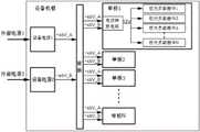
目前设备内部电源(-48V)备份硬件连接关系如图1所示。外部电源1和2分别接入到设备电源模块1和2后,再经过背板,送到个单板上,两组电源负载有设计冗余。当其中一路有问题时,另一路仍能够完全负担起整个设备的运行负载。The current device internal power supply (-48V) backup hardware connection relationship is shown in Figure 1. After the external power supplies 1 and 2 are connected to the power supply modules 1 and 2 of the equipment respectively, they are sent to a single board through the backplane. The two sets of power supply loads are designed for redundancy. When there is a problem with one of the paths, the other path can still fully bear the operating load of the entire equipment.
上述系统构成对整个设备供电的保护。板内主路电源故障率一般高于设备供电电源故障。当单板主路电源发生问题时,单板只能下电离线,业务切换到备份单板上去。如果是同一单板内部业务备份的情况,业务无法切换,只能中断。此外,在板内电源跌落后又恢复的情况中,板内信息会因掉电丢失,导致无法定位具体故障原因和故障位置。针对相关技术中单板主路电源缺乏保护的问题,现有技术还未提出有效的解决方案。The system described above constitutes the protection of the power supply to the entire device. The failure rate of the main circuit power supply in the board is generally higher than that of the equipment power supply. When the power supply of the main circuit of the board is faulty, the board can only be powered off and offline, and services are switched to the backup board. In the case of internal service backup on the same board, services cannot be switched and can only be interrupted. In addition, in the case that the power supply on the board is restored after being dropped, the information on the board will be lost due to power failure, making it impossible to locate the specific fault cause and fault location. Aiming at the problem of lack of protection of the main circuit power supply of the single board in the related art, the prior art has not yet proposed an effective solution.
发明内容SUMMARY OF THE INVENTION
本发明提供了一种电信设备及单板电源保护方法,解决了相关技术中单板主路电源缺乏保护的问题。The present invention provides a telecommunication equipment and a single-board power supply protection method, which solves the problem of lack of protection of the single-board main circuit power supply in the related art.
根据本发明的一个方面,提供一种电信设备,包括:设备电源、背板和第一单板和第二单板,该第一单板和该第二单板均包括板内负载器件,其中,该设备电源和该背板连接,该第一单板和该第二单板分别与该背板连接,其中该设备电源,用于向该背板提供电压;该背板,用于根据该设备电源提供的电压向该第一单板和该第二单板输出第一电压;该第一单板,用于将该第一电压转换为与自身板内负载器件相匹配的第二电压;该第二单板,用于将该第一电压转换为与自身板内负载器件相匹配的第三电压;该第一单板还用于在电压转换失败的情况下,接收由电压转换成功的第二单板提供的第三电压,该第二电压等于该第三电压。According to an aspect of the present invention, there is provided a telecommunication device, comprising: a device power supply, a backplane, and a first single board and a second single board, the first single board and the second single board both include on-board load devices, wherein , the equipment power supply is connected to the backplane, the first single board and the second single board are respectively connected to the backplane, wherein the equipment power supply is used to supply voltage to the backplane; the backplane is used to supply voltage to the backplane according to the The voltage provided by the device power supply outputs a first voltage to the first single board and the second single board; the first single board is used to convert the first voltage into a second voltage matching the load device in its own board; The second single board is used to convert the first voltage into a third voltage matching the load device in its own board; the first single board is also used to receive a voltage converted from a successful voltage conversion when the voltage conversion fails A third voltage provided by the second board, where the second voltage is equal to the third voltage.
进一步,该第二单板用于将该第三电压输出给该第一单板和自身板内负载器件。Further, the second single board is used for outputting the third voltage to the first single board and its own on-board load device.
进一步,该接收由电压转换成功的第二单板提供的第三电压包括:接收该背板提供的第三电压,该第三电压由该第二单板向该背板提供。Further, the receiving the third voltage provided by the second board whose voltage has been successfully converted includes: receiving the third voltage provided by the backplane, where the third voltage is provided by the second board to the backplane.
进一步,该第一单板和该第二单板还包括电源转换电路和电源切换电路,该电源转换电路与该电源切换电路相连,该电源切换电路与该板内负载器件相连;电源转换电路,用于将该第一电压转换为与自身板内负载器件相匹配的第二电压;电源切换电路,用于根据该电源转换电路的工作状态从该电源转换电路或该背板获取电压并传输给自身板内负载器件,该工作状态包括电压转换成功与电压转换失败。Further, the first single board and the second single board further include a power conversion circuit and a power switching circuit, the power conversion circuit is connected with the power switching circuit, and the power switching circuit is connected with the load device in the board; the power conversion circuit, It is used to convert the first voltage into a second voltage that matches the load device in its own board; the power switching circuit is used to obtain the voltage from the power conversion circuit or the backplane according to the working state of the power conversion circuit and transmit it to the Load device in its own board, the working status includes voltage conversion success and voltage conversion failure.
进一步,该电源切换电路包括第一开关电路和第三开关电路;该第一开关电路,用于通断该电源转换电路与该板内负载器件间的电路连接;该第三开关电路,用于通断该背板与该板内负载器件间的电路连接。Further, the power switching circuit includes a first switching circuit and a third switching circuit; the first switching circuit is used for switching on and off the circuit connection between the power switching circuit and the load device in the board; the third switching circuit is used for The circuit connection between the backplane and the load device in the board is turned on and off.
进一步,该电源切换电路还包括该第二开关电路,用于通断该将该电源转换电路与该背板间的电路连接。Further, the power switching circuit further includes the second switching circuit for switching on and off the circuit connection between the power switching circuit and the backplane.
进一步,该电源切换电路还包括电压监控模块,该电压监控模块用于在该电源转换电路电压转换失败的情况下接通该第三开关电路并断开该第一开关电路和该第二开关电路。Further, the power switching circuit further includes a voltage monitoring module, and the voltage monitoring module is configured to turn on the third switching circuit and disconnect the first switching circuit and the second switching circuit when the voltage switching of the power switching circuit fails .
根据本发明的另一方面,提供一种单板电源保护方法,应用于电信设备,该电信设备包括至少一个设备电源、背板和第一单板和第二单板,该第一单板和该第二单板均包括板内负载器件,包括:该设备电源向该背板提供电压;该背板根据该设备电源提供的电压向该第一单板和该第二单板输出第一电压;该第一单板将该第一电压转换为与自身板内负载器件相匹配的第二电压;该第二单板将该第一电压转换为与自身板内负载器件相匹配的第三电压;在电压转换失败的情况下,该第一单板接收由电压转换成功的第二单板提供的第三电压,该第二电压等于该第三电压。According to another aspect of the present invention, a single-board power protection method is provided, applied to a telecommunication device, the telecommunication device includes at least one device power supply, a backplane, and a first single board and a second single board, the first single board and Each of the second boards includes on-board load devices, including: the device power supply provides a voltage to the backplane; the backplane outputs a first voltage to the first board and the second board according to the voltage provided by the device power supply ; the first single board converts the first voltage into a second voltage matching the load device in its own board; the second single board converts the first voltage into a third voltage matching the load device in its own board ; In the case of voltage conversion failure, the first single board receives a third voltage provided by the second single board whose voltage conversion is successful, and the second voltage is equal to the third voltage.
进一步,在该第二单板将该第一电压转换为与自身板内负载器件相匹配的第三电压之后,该方法还包括:该第二单板将该第三电压输出给该第一单板和自身板内负载器件。Further, after the second single board converts the first voltage into a third voltage matching the load device in its own board, the method further includes: the second single board outputs the third voltage to the first single board board and its own on-board load devices.
进一步,该第二单板将该第三电压输出给该第一单板和自身板内负载器件包括:该第二单板将该第三电压输出给该背板和自身板内负载器件;该第一单板接收由电压转换成功的第二单板提供的第三电压包括:接收该背板提供的第三电压。Further, the second veneer outputting the third voltage to the first veneer and its own on-board load device includes: the second veneer outputting the third voltage to the backplane and its own on-board load device; the The first single board receiving the third voltage provided by the second single board whose voltage has been successfully converted includes: receiving the third voltage provided by the backplane.
进一步,该方法还包括:在检测到该第一电压转换得到的输出电压高于上限阈值或者低于下限阈值的情况下,该第一单板判定电压转换失败。Further, the method further includes: when it is detected that the output voltage obtained by converting the first voltage is higher than the upper threshold or lower than the lower threshold, the first board determines that the voltage conversion fails.
通过本发明,在第一单板电压转换失败的情况下,采用该第一单板接收由电压转换成功的第二单板提供的第三电压,该第二电压等于该第三电压的技术方案,解决了相关技术中单板主路电源缺乏保护的问题,为单板主路电源提供保护。Through the present invention, in the case that the voltage conversion of the first single board fails, the first single board receives the third voltage provided by the second single board whose voltage conversion is successful, and the second voltage is equal to the technical solution of the third voltage , which solves the problem of lack of protection of the single-board main circuit power supply in the related art, and provides protection for the single-board main circuit power supply.
附图说明Description of drawings
此处所说明的附图用来提供对本发明的进一步理解,构成本申请的一部分,本发明的示意性实施例及其说明用于解释本发明,并不构成对本发明的不当限定。在附图中:The accompanying drawings described herein are used to provide a further understanding of the present invention and constitute a part of the present application. The exemplary embodiments of the present invention and their descriptions are used to explain the present invention and do not constitute an improper limitation of the present invention. In the attached image:
图1是根据相关技术的电信设备内部电源相关硬件器件的结构示意图;1 is a schematic structural diagram of a power supply-related hardware device within a telecommunication device according to the related art;
图2是根据本发明实施例的电信设备的结构框图;2 is a structural block diagram of a telecommunication device according to an embodiment of the present invention;
图3是根据本发明优选实施例的电信设备的结构框图;3 is a structural block diagram of a telecommunication device according to a preferred embodiment of the present invention;
图4是根据本发明优选实施例的电信设备的电源切换电路的结构框图;4 is a structural block diagram of a power switching circuit of a telecommunication device according to a preferred embodiment of the present invention;
图5是根据本发明优选实施例的电信设备内部电源相关硬件器件的结构示意图;5 is a schematic structural diagram of an internal power supply-related hardware device of a telecommunication device according to a preferred embodiment of the present invention;
图6是根据本发明优选实施例的电源切换电路的结构示意图;6 is a schematic structural diagram of a power switching circuit according to a preferred embodiment of the present invention;
图7是根据本发明实施例的单板电源保护方法的流程图;7 is a flowchart of a method for protecting a power supply of a single board according to an embodiment of the present invention;
图8是根据本发明优选实施例的单板电源保护方法的流程图。FIG. 8 is a flowchart of a method for protecting a power supply of a single board according to a preferred embodiment of the present invention.
具体实施方式Detailed ways
下文中将参考附图并结合实施例来详细说明本发明。需要说明的是,在不冲突的情况下,本申请中的实施例及实施例中的特征可以相互组合。Hereinafter, the present invention will be described in detail with reference to the accompanying drawings and in conjunction with embodiments. It should be noted that the embodiments in the present application and the features of the embodiments may be combined with each other in the case of no conflict.
在本实施例中提供了一种电信设备及电源保护方法,图1是根据相关技术的电信设备内部电源相关硬件器件的结构示意图,如图1所示,以板内主路电源为12V为例,该电信设备包括:In this embodiment, a telecommunication device and a power supply protection method are provided. FIG. 1 is a schematic structural diagram of a hardware device related to an internal power supply of a telecommunication device according to the related art. As shown in FIG. 1 , the main circuit power supply in the board is 12V as an example. , the telecommunications equipment includes:
外部电源1和2分别与设备电源1和2连接,向其供电。设备电源1和设备电源2再经过背板,将48V电压送到各个单板上。其中,两组设备电源1和2的设计是出于负载冗余,也即当其中一路有问题时,另一路仍能够完全负担起整个设备的运行负载。背板中包括电源转换电路和板内负载器件,电源转换电路接收到背板输送的48V电压将其转换为12V电压,提供给板内负载器件。External power sources 1 and 2 are respectively connected to device power sources 1 and 2 to supply power to them. The device power supply 1 and the device power supply 2 pass through the backplane and send the 48V voltage to each single board. Among them, the two sets of equipment power supplies 1 and 2 are designed for load redundancy, that is, when one of the power supplies has a problem, the other can still fully bear the operating load of the entire equipment. The backplane includes a power conversion circuit and an on-board load device. The power conversion circuit receives the 48V voltage delivered by the backplane, converts it into a 12V voltage, and provides it to the on-board load device.
在单板主路电源发生故障也即电压转换失败的情况下,设备单板发出离线告警,该告警用于警示业务中断,触发业务倒换机制。在同一单板内进行业务保护的情况下,业务中断;在跨单板进行业务保护的情况下,业务倒换至备份单板。针对相关技术中单板主路电源在同单板进行业务保护的情况下容易发生业务中断的问题,本发明提供如下实施例来解决。When the power supply of the main circuit of the board fails, that is, the voltage conversion fails, the equipment board issues an offline alarm, which is used to warn the service interruption and trigger the service switching mechanism. In the case of service protection within the same board, the service is interrupted; in the case of service protection across boards, the service is switched to the backup board. Aiming at the problem in the related art that the main circuit power supply of a single board is prone to service interruption when the same board is used for service protection, the present invention provides the following embodiments to solve the problem.
图2是根据本发明实施例的电信设备的结构框图,如图2所示,该电信设备包括设备电源22、背板24和第一单板26和第二单板28,该第一单板26包括至少一个板内负载器件262,该第二单板28包括至少一个板内负载器件282,其中,该设备电源22和该背板24连接,该第一单板26和该第二单板28分别与该背板24连接,其中:FIG. 2 is a structural block diagram of a telecommunication device according to an embodiment of the present invention. As shown in FIG. 2 , the telecommunication device includes a device power supply 22 , a backplane 24 , a
该设备电源22,用于向该背板24提供电压;the device power supply 22 for supplying voltage to the backplane 24;
该背板24,用于根据该设备电源22提供的电压向该第一单板26和该第二单板28输出第一电压;The backplane 24 is used for outputting a first voltage to the first
该第一单板26,用于将该第一电压转换为与自身板内负载器件262相匹配的第二电压;The first
该第二单板28,用于将该第一电压转换为与自身板内负载器件282相匹配的第三电压;The second
该第一单板26还用于在电压转换失败的情况下,接收由电压转换成功的第二单板28提供的第三电压,该第二电压等于该第三电压。The first
优选地,该第二单板28还用于将该第三电压输出给该第一单板26和自身板内负载器件282。Preferably, the second
优选地,该第一单板26通过以下方式接收由电压转换成功的第二单板28提供的第三电压:该第一单板26接收该背板24提供的第三电压,该第三电压由该第二单板28向该背板24提供。Preferably, the first
在本实施例中第一单板26作为被保护单板,第二单板28作为保护单板在第一单板26电压转换失败的情况下向其提供板内负载器件262所需的电压。值得一提的是,该电信设备保护M块单板,其中N块单板具备作为保护单板的能力可在电信设备内的其他单板电压转换失败的情况下为其板内负载器件供电,其中M≥2,N≤M。In this embodiment, the
图3是根据本发明优选实施例的电信设备,如图3所示,该第一单板26还包括电源转换电路264和电源切换电路266,该电源转换电路264与该电源切换电路266相连,该电源切换电路266与该板内负载器件262相连:FIG. 3 is a telecommunication device according to a preferred embodiment of the present invention. As shown in FIG. 3, the first
电源转换电路264,用于将该第一电压转换为与自身板内负载器件262相匹配的第二电压;a power conversion circuit 264 for converting the first voltage into a second voltage matching the
电源切换电路266,用于根据该电源转换电路264的工作状态从该电源转换电路264或该背板24获取电压并传输给自身板内负载器件262,该工作状态包括电压转换成功与电压转换失败。The power switching circuit 266 is used to obtain the voltage from the power converting circuit 264 or the backplane 24 according to the working state of the power converting circuit 264 and transmit it to the
优选地,该电源切换电路266可以通过开关电路来实现电源转换电路264或背板24向板内负载器件262输出电压。该电源切换电路286可以通过开关电路来实现第三电压向背板24的电压输出。Preferably, the power switching circuit 266 can implement the power switching circuit 264 or the backplane 24 to output voltage to the on-
图4是根据本发明优选实施例的电信设备的电源切换电路的结构框图,如图4所示,该电源切换电路包括:FIG. 4 is a structural block diagram of a power switching circuit of a telecommunication device according to a preferred embodiment of the present invention. As shown in FIG. 4 , the power switching circuit includes:
该第一开关电路44,用于通断该电源转换电路与该板内负载器件间的电路连接;The first switch circuit 44 is used to turn on and off the circuit connection between the power conversion circuit and the load device in the board;
该第三开关电路48,用于通断该背板与该板内负载器件间的电路连接。The third switch circuit 48 is used to turn on and off the circuit connection between the backplane and the load device in the board.
优选地,该电源切换电路还包括第二开关电路46,用于通断该将该电源转换电路与该背板间的电路连接。Preferably, the power switching circuit further includes a second switching circuit 46 for switching on and off the circuit connection between the power switching circuit and the backplane.
优选地,该电源切换电路还包括电压监控模块42,该电压监控模块42用于在该电源转换电路电压转换失败的情况下接通该第三开关电路48并断开该第一开关电路44和该第二开关电路46。Preferably, the power switching circuit further includes a voltage monitoring module 42, and the voltage monitoring module 42 is configured to turn on the third switching circuit 48 and turn off the first switching circuit 44 and The second switch circuit 46 .
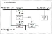
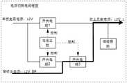
图5是根据本发明优选实施例的电信设备内部电源相关硬件器件的结构示意图,如图5所示,该电信设备包括设备电源1和设备电源2,分别接收外部电源1和外部电源2传输的电压,同时将48V的电压加载到背板上。该背板将从设备电源1和设备电源2得到的48V电压均加载在每个单板,以单板1为例,包括电源转换电路、电源切换电路和至少一块板内负载器件。单板1中的电源转换电路接收背板提供的48V电压,并将其转换为12V电路加载在电源切换电路上。在电源转换成功的情况下,电源切换电路将转换得到的12V电压回传给背板并将12V电压加载在每一块板内负载器件上,12V为本实施例中板内负载器件的工作电压。在电源转换失败的情况下,电源切换电路从背板上获取12V电压加载到每个板内负载器件上,该背板提供的12V电压是其他电源转换成功的单板向其提供的。FIG. 5 is a schematic structural diagram of a hardware device related to the internal power supply of a telecommunication device according to a preferred embodiment of the present invention. As shown in FIG. 5 , the telecommunication device includes a device power supply 1 and a device power supply 2, which respectively receive the transmission of the external power supply 1 and the external power supply 2. voltage, while loading 48V to the backplane. The backplane loads the 48V voltage obtained from the device power supply 1 and the device power supply 2 to each single board. Taking the single board 1 as an example, it includes a power conversion circuit, a power switching circuit and at least one on-board load device. The power conversion circuit in the single board 1 receives the 48V voltage provided by the backplane, and converts it into a 12V circuit and loads it on the power switch circuit. In the case of successful power conversion, the power switching circuit returns the converted 12V voltage to the backplane and loads the 12V voltage on each load device in the board, 12V is the working voltage of the load device in the board in this embodiment. In the case of power conversion failure, the power switching circuit obtains 12V from the backplane and loads it on each on-board load device. The 12V voltage provided by the backplane is provided by other boards that have successfully converted the power supply.
图6是根据本发明优选实施例的电源切换电路的结构示意图,如图6-1、6-2和6-3所示,所示电源切换电路包括电压监控和开关电路1、开关电路2和开关电路3。电压监控模块通过实时监控单板主路电源的状态,通过控制开关电路1、2、3,让单板主路电源与板内负载器件、背板之间电路的导通和断开。6 is a schematic structural diagram of a power supply switching circuit according to a preferred embodiment of the present invention, as shown in FIGS. 6-1, 6-2 and 6-3, the shown power supply switching circuit includes a voltage monitoring and switching circuit 1, a switching circuit 2 and switch circuit 3. The voltage monitoring module monitors the status of the main circuit power supply of the single board in real time, and controls the switch circuits 1, 2 and 3 to make the circuit between the main circuit power supply of the single board and the load device and the backplane on and off the board.
初次上电时,默认电源转换电路与背板断开,电源转换电路与板内负载器件之间断开。当监控模块确认电源转换电路输出正常时,打开电源转换电路与背板之间的开关电路1,并同时打开电源转换电路与板内负载器件之间的开关电路2,使得电源转换电路得到的12V电压可以向板内负载器件和背板供电。当故障单板的主干电源发生问题后,监控模块关闭电源转换电路与背板之间的开关电路1,并关闭电源转换电路与板内负载器件之间的开关电路2。同时打开背板主电源到板上负载的开关电路3,完成板内电源的切换。优选地,切换动作需要快速的进行,以增加储能模块保证切换过程中的稳定性。When powered on for the first time, the default power conversion circuit is disconnected from the backplane, and the power conversion circuit is disconnected from the load device on the board. When the monitoring module confirms that the output of the power conversion circuit is normal, it opens the switch circuit 1 between the power conversion circuit and the backplane, and simultaneously opens the switch circuit 2 between the power conversion circuit and the on-board load device, so that the 12V output from the power conversion circuit The voltage can power on-board load devices and the backplane. When there is a problem with the main power supply of the faulty board, the monitoring module turns off the switch circuit 1 between the power conversion circuit and the backplane, and turns off the switch circuit 2 between the power conversion circuit and the on-board load device. At the same time, turn on the main power supply of the backplane to the switch circuit 3 of the load on the board to complete the switching of the power supply in the board. Preferably, the switching action needs to be performed quickly, so as to increase the stability of the energy storage module during the switching process.
优选地,电压监控模块根据电源切换电路输出的电压判断电源转换是否成功。具体的,电压监控模块监控到电源转换电路输出电压超出额定范围内的情况下,判定电源转换电路转换失败,其中额定范围是指大于最小阈值,小于最大阈值,板内负载期间的工作电压在额定范围内。Preferably, the voltage monitoring module determines whether the power conversion is successful according to the voltage output by the power switching circuit. Specifically, when the voltage monitoring module monitors that the output voltage of the power conversion circuit exceeds the rated range, it determines that the conversion of the power conversion circuit fails. within the range.
图7是根据本发明实施例的单板电源保护方法的流程图,如图7所示,所示单板电源保护方法应用于电信设备,该电信设备包括至少一个设备电源、背板和第一单板和第二单板,该第一单板和该第二单板均包括板内负载器件,包括:FIG. 7 is a flowchart of a single-board power protection method according to an embodiment of the present invention. As shown in FIG. 7 , the shown single-board power protection method is applied to a telecommunication device, and the telecommunication device includes at least one device power supply, a backplane and a first A single board and a second single board, the first single board and the second single board both include on-board load components, including:
步骤S702,该设备电源向该背板提供电压;Step S702, the device power supply provides voltage to the backplane;
步骤S704,该背板根据该设备电源提供的电压向该第一单板和该第二单板输出第一电压;Step S704, the backplane outputs a first voltage to the first single board and the second single board according to the voltage provided by the device power supply;
步骤S706,该第一单板将该第一电压转换为与自身板内负载器件相匹配的第二电压;Step S706, the first single board converts the first voltage into a second voltage matching the load device in its own board;
步骤S708,该第二单板将该第一电压转换为与自身板内负载器件相匹配的第三电压;Step S708, the second single board converts the first voltage into a third voltage matching the load device in its own board;
优选地,第二单板将该第三电压输出给该第一单板和自身板内负载器件。更进一步地,该第二单板将该第三电压输出给该背板和自身板内负载器件;该第一单板接收由电压转换成功的第二单板提供的第三电压包括:接收该背板提供的第三电压。Preferably, the second single board outputs the third voltage to the first single board and its own on-board load device. Furthermore, the second single board outputs the third voltage to the backplane and its own on-board load device; the first single board receiving the third voltage provided by the second single board whose voltage has been successfully converted includes: receiving the The third voltage provided by the backplane.
步骤S710,在电压转换失败的情况下,该第一单板接收由电压转换成功的第二单板提供的第三电压,该第二电压等于该第三电压。Step S710, in the case that the voltage conversion fails, the first board receives a third voltage provided by the second board whose voltage conversion is successful, where the second voltage is equal to the third voltage.
优选地,在检测到该第一电压转换得到的输出电压高于上限阈值或者低于下限阈值的情况下,该第一单板判定电压转换失败。Preferably, the first board determines that the voltage conversion fails when it is detected that the output voltage obtained by converting the first voltage is higher than the upper threshold or lower than the lower threshold.
图8是根据本发明优选实施例的单板电源保护方法的流程图,如图8所示,所示方法包括:FIG. 8 is a flowchart of a method for protecting a power supply of a single board according to a preferred embodiment of the present invention. As shown in FIG. 8 , the method includes:
步骤S802,单板上电;Step S802, the board is powered on;
步骤S804,关闭单板主路电源与背板主电源连接开关2,也即电源切换电路与背板之间的开关电路2;Step S804, turning off the connection switch 2 between the main circuit power supply of the single board and the main power supply of the backplane, that is, the switch circuit 2 between the power switching circuit and the backplane;
步骤S806,关闭背板主电源与单板负载连接开关电路3,也即板内负载器件与背板之间的开关电路3;Step S806, turn off the main power supply of the backplane and the switch circuit 3 connected to the single-board load, that is, the switch circuit 3 between the load device in the board and the backplane;
步骤S808,判断单板主路电源是否处于正常工作状态;若判断结果为是则执行步骤S810,若判断结果为否则执行步骤S812;Step S808, judging whether the main circuit power supply of the single board is in a normal working state; if the judgment result is yes, execute step S810; if the judgment result is otherwise, execute step S812;
步骤S810,打开开关电路1和开关电路2,接通电源转换电路与板内负载器件,及电源转换电路与背板之间的电路连接;Step S810, turn on the switch circuit 1 and the switch circuit 2, connect the power conversion circuit and the on-board load device, and the circuit connection between the power conversion circuit and the backplane;
步骤S812,关闭单板主路电源与背板自电源连接的开关电路2;Step S812, turning off the switch circuit 2 connecting the main circuit power supply of the single board and the self power supply of the backplane;
步骤S814,关闭单板主路电源与板上负载连接开关电路1;Step S814, turning off the main circuit power supply of the single board and the on-board load connection switch circuit 1;
步骤S816,打开背板主电源与单板负载连接的开关电路3;Step S816, turn on the switch circuit 3 connecting the main power supply of the backplane and the single-board load;
步骤S818,电源故障告警。Step S818, power failure alarm.
显然,本领域的技术人员应该明白,上述的本发明的各模块或各步骤可以用通用的计算装置来实现,它们可以集中在单个的计算装置上,或者分布在多个计算装置所组成的网络上,可选地,它们可以用计算装置可执行的程序代码来实现,从而,可以将它们存储在存储装置中由计算装置来执行,并且在某些情况下,可以以不同于此处的顺序执行所示出或描述的步骤,或者将它们分别制作成各个集成电路模块,或者将它们中的多个模块或步骤制作成单个集成电路模块来实现。这样,本发明不限制于任何特定的硬件和软件结合。Obviously, those skilled in the art should understand that the above-mentioned modules or steps of the present invention can be implemented by a general-purpose computing device, which can be centralized on a single computing device, or distributed in a network composed of multiple computing devices Alternatively, they may be implemented in program code executable by a computing device, such that they may be stored in a storage device and executed by the computing device, and in some cases, in a different order than here The steps shown or described are performed either by fabricating them separately into individual integrated circuit modules, or by fabricating multiple modules or steps of them into a single integrated circuit module. As such, the present invention is not limited to any particular combination of hardware and software.
以上该仅为本发明的优选实施例而已,并不用于限制本发明,对于本领域的技术人员来说,本发明可以有各种更改和变化。凡在本发明的精神和原则之内,所作的任何修改、等同替换、改进等,均应包括在本发明的保护范围之内。The above are only preferred embodiments of the present invention, and are not intended to limit the present invention. For those skilled in the art, the present invention may have various modifications and changes. Any modification, equivalent replacement, improvement, etc. made within the spirit and principle of the present invention shall be included within the protection scope of the present invention.
Claims (11)
Priority Applications (2)
| Application Number | Priority Date | Filing Date | Title |
|---|---|---|---|
| CN201910154579.XACN111628652A (en) | 2019-02-28 | 2019-02-28 | A kind of telecommunications equipment and single board power protection method |
| PCT/CN2020/073159WO2020173259A1 (en) | 2019-02-28 | 2020-01-20 | Telecommunication device and single board power supply protection method |
Applications Claiming Priority (1)
| Application Number | Priority Date | Filing Date | Title |
|---|---|---|---|
| CN201910154579.XACN111628652A (en) | 2019-02-28 | 2019-02-28 | A kind of telecommunications equipment and single board power protection method |
Publications (1)
| Publication Number | Publication Date |
|---|---|
| CN111628652Atrue CN111628652A (en) | 2020-09-04 |
Family
ID=72238797
Family Applications (1)
| Application Number | Title | Priority Date | Filing Date |
|---|---|---|---|
| CN201910154579.XAPendingCN111628652A (en) | 2019-02-28 | 2019-02-28 | A kind of telecommunications equipment and single board power protection method |
Country Status (2)
| Country | Link |
|---|---|
| CN (1) | CN111628652A (en) |
| WO (1) | WO2020173259A1 (en) |
Citations (6)
| Publication number | Priority date | Publication date | Assignee | Title |
|---|---|---|---|---|
| CN101159385A (en)* | 2002-08-02 | 2008-04-09 | 华为技术有限公司 | A single-board power backup method and a single-board power backup system |
| CN203086179U (en)* | 2012-12-25 | 2013-07-24 | 比亚迪股份有限公司 | Double-voltage DC supply system |
| CN103744467A (en)* | 2013-12-16 | 2014-04-23 | 浙江大学 | Maximum power tracking device for solar cell of miniature satellite power system and control method thereof |
| US20140277802A1 (en)* | 2013-03-12 | 2014-09-18 | Alpha And Omega Semiconductor Incorporated | Fault tolerant power supply incorporating intelligent load switch to provide uninterrupted power |
| US20160049795A1 (en)* | 2014-08-14 | 2016-02-18 | Zodiac Aero Electric | Supply system for electronic boards of an electrical distribution system |
| CN106249838A (en)* | 2016-08-11 | 2016-12-21 | 华为技术有限公司 | Method, backboard and the server powered for server |
Family Cites Families (5)
| Publication number | Priority date | Publication date | Assignee | Title |
|---|---|---|---|---|
| JP5029068B2 (en)* | 2007-03-01 | 2012-09-19 | 富士通株式会社 | Wireless base station |
| CN101257391B (en)* | 2008-04-21 | 2010-12-08 | 中兴通讯股份有限公司 | Single board managing method for miniature electric communication computing structure standard |
| CN101867221B (en)* | 2010-06-28 | 2014-02-05 | 中兴通讯股份有限公司 | Single board and method for power monitoring in board |
| CN102883355B (en)* | 2011-07-11 | 2014-12-10 | 中国移动通信集团公司 | Building base band unit, base band processing board and fault processing method for base band processing board |
| CN203218961U (en)* | 2013-02-04 | 2013-09-25 | 南京丰泰通信技术股份有限公司 | Low voltage DC power pack power strip backup apparatus for communication device group |
- 2019
- 2019-02-28CNCN201910154579.XApatent/CN111628652A/enactivePending
- 2020
- 2020-01-20WOPCT/CN2020/073159patent/WO2020173259A1/ennot_activeCeased
Patent Citations (6)
| Publication number | Priority date | Publication date | Assignee | Title |
|---|---|---|---|---|
| CN101159385A (en)* | 2002-08-02 | 2008-04-09 | 华为技术有限公司 | A single-board power backup method and a single-board power backup system |
| CN203086179U (en)* | 2012-12-25 | 2013-07-24 | 比亚迪股份有限公司 | Double-voltage DC supply system |
| US20140277802A1 (en)* | 2013-03-12 | 2014-09-18 | Alpha And Omega Semiconductor Incorporated | Fault tolerant power supply incorporating intelligent load switch to provide uninterrupted power |
| CN103744467A (en)* | 2013-12-16 | 2014-04-23 | 浙江大学 | Maximum power tracking device for solar cell of miniature satellite power system and control method thereof |
| US20160049795A1 (en)* | 2014-08-14 | 2016-02-18 | Zodiac Aero Electric | Supply system for electronic boards of an electrical distribution system |
| CN106249838A (en)* | 2016-08-11 | 2016-12-21 | 华为技术有限公司 | Method, backboard and the server powered for server |
Also Published As
| Publication number | Publication date |
|---|---|
| WO2020173259A1 (en) | 2020-09-03 |
Similar Documents
| Publication | Publication Date | Title |
|---|---|---|
| US10129617B2 (en) | Link switching method, device, and system | |
| CN102292938B (en) | An electronic repair device | |
| US20080141070A1 (en) | Method and apparatus for correlating an out-of-range condition to a particular power connection | |
| US7898106B2 (en) | DC UPS configured as intrinsic power transfer switch | |
| EP4084492A1 (en) | A method, system and olt for dual-parenting pon protection | |
| US20090315395A1 (en) | Fieldbus system with shared redundancy system | |
| US10539992B2 (en) | Redundant power extender | |
| CN111628652A (en) | A kind of telecommunications equipment and single board power protection method | |
| US7206963B2 (en) | System and method for providing switch redundancy between two server systems | |
| CN101841241B (en) | Assembly with DC electricity supply units switch in parallel | |
| JP7417773B1 (en) | Network interface card and transmission performance monitoring method | |
| US9461883B2 (en) | Coupling device for a data transmission network and data transmission network | |
| CN105553735A (en) | Stacking system fault handling method, equipment and stacking system | |
| US8212387B2 (en) | Connection module for providing N+N and M+1 redundant power distribution | |
| EP2319208B1 (en) | Absolute control of virtual switches | |
| US20090019140A1 (en) | Method for backup switching spatially separated switching systems | |
| JP3307603B2 (en) | UPS device capable of mutual monitoring and supply of power supply | |
| US20070014166A1 (en) | Redundancy power for communication devices | |
| US8406121B2 (en) | Method for error detection in a packet-based message distribution system | |
| CN109510725A (en) | Fault testing system of communication equipment and method | |
| CN109861871B (en) | Ethernet bypass equipment with self-monitoring function | |
| US7131028B2 (en) | System and method for interconnecting nodes of a redundant computer system | |
| CN111830856B (en) | Train master control system | |
| EP2432152B1 (en) | Method and apparatus for switching the main/standby single board | |
| KR100947759B1 (en) | Malfunction detection device and multi-board system using same |
Legal Events
| Date | Code | Title | Description |
|---|---|---|---|
| PB01 | Publication | ||
| PB01 | Publication | ||
| SE01 | Entry into force of request for substantive examination | ||
| SE01 | Entry into force of request for substantive examination |