CN111627989A - Method for manufacturing ultra-fine transistor by using thin film layer - Google Patents
Method for manufacturing ultra-fine transistor by using thin film layerDownload PDFInfo
- Publication number
- CN111627989A CN111627989ACN202010481884.2ACN202010481884ACN111627989ACN 111627989 ACN111627989 ACN 111627989ACN 202010481884 ACN202010481884 ACN 202010481884ACN 111627989 ACN111627989 ACN 111627989A
- Authority
- CN
- China
- Prior art keywords
- metal electrode
- film
- layer
- thin film
- substrate
- Prior art date
- Legal status (The legal status is an assumption and is not a legal conclusion. Google has not performed a legal analysis and makes no representation as to the accuracy of the status listed.)
- Granted
Links
- 238000000034methodMethods0.000titleclaimsabstractdescription32
- 239000010409thin filmSubstances0.000titleclaimsabstractdescription27
- 238000004519manufacturing processMethods0.000titleclaimsabstractdescription12
- 229910052751metalInorganic materials0.000claimsabstractdescription46
- 239000002184metalSubstances0.000claimsabstractdescription46
- 239000010408filmSubstances0.000claimsabstractdescription31
- 239000000463materialSubstances0.000claimsabstractdescription29
- 239000000758substrateSubstances0.000claimsabstractdescription27
- 238000012546transferMethods0.000claimsabstractdescription11
- 238000000151depositionMethods0.000claimsabstractdescription9
- 239000003989dielectric materialSubstances0.000claimsabstractdescription9
- 229920000642polymerPolymers0.000claimsabstractdescription9
- 230000005669field effectEffects0.000claimsabstractdescription7
- 230000035939shockEffects0.000claimsabstractdescription6
- 239000011261inert gasSubstances0.000claimsabstractdescription5
- 230000008569processEffects0.000claimsabstractdescription5
- 238000000137annealingMethods0.000claimsdescription7
- 238000005530etchingMethods0.000claimsdescription6
- 238000005520cutting processMethods0.000claimsdescription5
- 238000002955isolationMethods0.000claimsdescription5
- 229910052798chalcogenInorganic materials0.000claimsdescription4
- 150000001787chalcogensChemical class0.000claimsdescription4
- 238000010521absorption reactionMethods0.000claimsdescription3
- 230000004907fluxEffects0.000claimsdescription3
- 229910016001MoSeInorganic materials0.000claimsdescription2
- 239000001307heliumSubstances0.000claimsdescription2
- 229910052734heliumInorganic materials0.000claimsdescription2
- SWQJXJOGLNCZEY-UHFFFAOYSA-Nhelium atomChemical compound[He]SWQJXJOGLNCZEY-UHFFFAOYSA-N0.000claimsdescription2
- 229910052750molybdenumInorganic materials0.000claimsdescription2
- 229910052711seleniumInorganic materials0.000claimsdescription2
- 229910052717sulfurInorganic materials0.000claimsdescription2
- 229910052714telluriumInorganic materials0.000claimsdescription2
- 229910052721tungstenInorganic materials0.000claimsdescription2
- 239000004593EpoxySubstances0.000claims1
- 230000001276controlling effectEffects0.000abstractdescription2
- 239000002090nanochannelSubstances0.000abstractdescription2
- 230000001105regulatory effectEffects0.000abstractdescription2
- 239000010410layerSubstances0.000description32
- 238000010586diagramMethods0.000description10
- 239000003822epoxy resinSubstances0.000description8
- 229920003229poly(methyl methacrylate)Polymers0.000description8
- 229920000647polyepoxidePolymers0.000description8
- 239000004926polymethyl methacrylateSubstances0.000description8
- XUIMIQQOPSSXEZ-UHFFFAOYSA-NSiliconChemical compound[Si]XUIMIQQOPSSXEZ-UHFFFAOYSA-N0.000description5
- 229910052710siliconInorganic materials0.000description5
- 239000010703siliconSubstances0.000description5
- XKRFYHLGVUSROY-UHFFFAOYSA-NArgonChemical compound[Ar]XKRFYHLGVUSROY-UHFFFAOYSA-N0.000description4
- 238000011161developmentMethods0.000description4
- 238000005516engineering processMethods0.000description3
- 229910052594sapphireInorganic materials0.000description3
- 239000010980sapphireSubstances0.000description3
- 239000004065semiconductorSubstances0.000description3
- CSCPPACGZOOCGX-UHFFFAOYSA-NAcetoneChemical compoundCC(C)=OCSCPPACGZOOCGX-UHFFFAOYSA-N0.000description2
- 229910052786argonInorganic materials0.000description2
- 238000000231atomic layer depositionMethods0.000description2
- QVGXLLKOCUKJST-UHFFFAOYSA-Natomic oxygenChemical compound[O]QVGXLLKOCUKJST-UHFFFAOYSA-N0.000description2
- 238000005229chemical vapour depositionMethods0.000description2
- 229910052760oxygenInorganic materials0.000description2
- 239000001301oxygenSubstances0.000description2
- 238000000206photolithographyMethods0.000description2
- 238000005240physical vapour depositionMethods0.000description2
- 238000001020plasma etchingMethods0.000description2
- 238000011160researchMethods0.000description2
- IJGRMHOSHXDMSA-UHFFFAOYSA-NAtomic nitrogenChemical compoundN#NIJGRMHOSHXDMSA-UHFFFAOYSA-N0.000description1
- 229910052582BNInorganic materials0.000description1
- PZNSFCLAULLKQX-UHFFFAOYSA-NBoron nitrideChemical compoundN#BPZNSFCLAULLKQX-UHFFFAOYSA-N0.000description1
- OKTJSMMVPCPJKN-UHFFFAOYSA-NCarbonChemical compound[C]OKTJSMMVPCPJKN-UHFFFAOYSA-N0.000description1
- LFQSCWFLJHTTHZ-UHFFFAOYSA-NEthanolChemical compoundCCOLFQSCWFLJHTTHZ-UHFFFAOYSA-N0.000description1
- UFHFLCQGNIYNRP-UHFFFAOYSA-NHydrogenChemical compound[H][H]UFHFLCQGNIYNRP-UHFFFAOYSA-N0.000description1
- 229910052782aluminiumInorganic materials0.000description1
- XAGFODPZIPBFFR-UHFFFAOYSA-NaluminiumChemical compound[Al]XAGFODPZIPBFFR-UHFFFAOYSA-N0.000description1
- 230000009286beneficial effectEffects0.000description1
- 230000005540biological transmissionEffects0.000description1
- 239000000969carrierSubstances0.000description1
- 238000005234chemical depositionMethods0.000description1
- 239000008367deionised waterSubstances0.000description1
- 229910021641deionized waterInorganic materials0.000description1
- 229910003460diamondInorganic materials0.000description1
- 239000010432diamondSubstances0.000description1
- 229910001873dinitrogenInorganic materials0.000description1
- 230000000694effectsEffects0.000description1
- 238000000313electron-beam-induced depositionMethods0.000description1
- 239000011888foilSubstances0.000description1
- 229910002804graphiteInorganic materials0.000description1
- 239000010439graphiteSubstances0.000description1
- 239000001257hydrogenSubstances0.000description1
- 229910052739hydrogenInorganic materials0.000description1
- 230000003116impacting effectEffects0.000description1
- 238000009776industrial productionMethods0.000description1
- 230000010354integrationEffects0.000description1
- 238000001459lithographyMethods0.000description1
- 238000001755magnetron sputter depositionMethods0.000description1
- 229910052754neonInorganic materials0.000description1
- GKAOGPIIYCISHV-UHFFFAOYSA-Nneon atomChemical compound[Ne]GKAOGPIIYCISHV-UHFFFAOYSA-N0.000description1
- 238000005289physical depositionMethods0.000description1
- 238000003672processing methodMethods0.000description1
- 230000001737promoting effectEffects0.000description1
- 238000004549pulsed laser depositionMethods0.000description1
- 239000011347resinSubstances0.000description1
- 229920005989resinPolymers0.000description1
- 238000000926separation methodMethods0.000description1
- 239000002356single layerSubstances0.000description1
- XLYOFNOQVPJJNP-UHFFFAOYSA-NwaterChemical compoundOXLYOFNOQVPJJNP-UHFFFAOYSA-N0.000description1
Images


Classifications
- H—ELECTRICITY
- H10—SEMICONDUCTOR DEVICES; ELECTRIC SOLID-STATE DEVICES NOT OTHERWISE PROVIDED FOR
- H10D—INORGANIC ELECTRIC SEMICONDUCTOR DEVICES
- H10D64/00—Electrodes of devices having potential barriers
- H10D64/01—Manufacture or treatment
- B—PERFORMING OPERATIONS; TRANSPORTING
- B82—NANOTECHNOLOGY
- B82Y—SPECIFIC USES OR APPLICATIONS OF NANOSTRUCTURES; MEASUREMENT OR ANALYSIS OF NANOSTRUCTURES; MANUFACTURE OR TREATMENT OF NANOSTRUCTURES
- B82Y30/00—Nanotechnology for materials or surface science, e.g. nanocomposites
- H—ELECTRICITY
- H10—SEMICONDUCTOR DEVICES; ELECTRIC SOLID-STATE DEVICES NOT OTHERWISE PROVIDED FOR
- H10D—INORGANIC ELECTRIC SEMICONDUCTOR DEVICES
- H10D30/00—Field-effect transistors [FET]
- H—ELECTRICITY
- H10—SEMICONDUCTOR DEVICES; ELECTRIC SOLID-STATE DEVICES NOT OTHERWISE PROVIDED FOR
- H10D—INORGANIC ELECTRIC SEMICONDUCTOR DEVICES
- H10D30/00—Field-effect transistors [FET]
- H10D30/01—Manufacture or treatment
Landscapes
- Chemical & Material Sciences (AREA)
- Engineering & Computer Science (AREA)
- Nanotechnology (AREA)
- Physics & Mathematics (AREA)
- Composite Materials (AREA)
- Condensed Matter Physics & Semiconductors (AREA)
- General Physics & Mathematics (AREA)
- Materials Engineering (AREA)
- Crystallography & Structural Chemistry (AREA)
- Thin Film Transistor (AREA)
- Insulated Gate Type Field-Effect Transistor (AREA)
Abstract
Translated fromChinese
Description
Translated fromChinese技术领域technical field
本发明属于场效应晶体管领域,具体涉及一种薄膜层用于制造超精细晶体管的方法。The invention belongs to the field of field effect transistors, and in particular relates to a method for manufacturing a superfine transistor with a thin film layer.
背景技术Background technique
集成电路芯片作为现代电子信息技术的基础,具有功能强、功耗低、速度快和成本低的特点。戈登·摩尔先生曾经对半导体行业的发展做出了预测,即著名的摩尔定律。在最初的几十年中,集成电路的发展基本遵循摩尔定律。摩尔定律能够生效的前提就是器件能够持续小型化,即器件的沟道长度不断缩小。当器件特征尺寸不断地按比例缩小时,载流子在沟道中传输时几乎不会遇到散射,称之为弹道输运。因此,如何缩小晶体管沟道的长度,提升弹道输运效率,使集成电路芯片能支持越来越多的功能,同时降低芯片的成本、提高电路的等效集成度已经成为场效应晶体管领域技术研究人员的研究重点。As the basis of modern electronic information technology, integrated circuit chip has the characteristics of strong function, low power consumption, high speed and low cost. Mr. Gordon Moore once predicted the development of the semiconductor industry, the famous Moore's Law. In the first few decades, the development of integrated circuits basically followed Moore's Law. The premise that Moore's Law can take effect is that the device can continue to be miniaturized, that is, the channel length of the device continues to shrink. As device feature sizes continue to be scaled down, carriers travel in the channel with little or no scattering, which is called ballistic transport. Therefore, how to reduce the length of the transistor channel, improve the ballistic transport efficiency, enable the integrated circuit chip to support more and more functions, reduce the cost of the chip, and improve the equivalent integration of the circuit has become a technical research in the field of field effect transistors research focus of personnel.
在晶体管制造工艺中,如何减小两金属电极之间的间隙是实现短沟道长度的关键。现有技术在制备晶体管沟道时,不论是光刻技术还是直接加工的方法都存在了困难。制造亚十纳米级的小尺寸沟道,已经超出了绝大多数设备的极限。另外,即便可以制备超短沟道,成本和质量也不易控制。目前一台高分辨率的光刻机的成本在1亿美金以上。简单有效地制造亚十纳米间隙仍然是一个挑战,有必要开发低成本地制造大面积纳米间隙的方法。In the transistor manufacturing process, how to reduce the gap between the two metal electrodes is the key to realizing the short channel length. In the prior art, there are difficulties in preparing the transistor channel, whether it is a photolithography technique or a direct processing method. Fabricating small-scale channels on the sub-ten nanometer scale is beyond the limits of most devices. In addition, even if ultra-short channels can be fabricated, the cost and quality are not easy to control. At present, the cost of a high-resolution lithography machine is more than 100 million US dollars. Simple and efficient fabrication of sub-ten-nanometer gaps remains a challenge, and it is necessary to develop low-cost methods to fabricate large-area nanogaps.
发明内容SUMMARY OF THE INVENTION
本发明的目的在于提供一种薄膜层用于制造超精细晶体管的方法,为突破摩尔定律带来的物理极限,推动半导体产业的发展提供了一条新的道路。The purpose of the present invention is to provide a method for manufacturing ultrafine transistors with thin film layers, which provides a new path for breaking through the physical limit brought by Moore's law and promoting the development of the semiconductor industry.
本发明实现目的所采用的方案是:一种薄膜层用于制造超精细晶体管的方法,包括以下步骤:The scheme adopted by the present invention to achieve the object is: a method for a thin film layer to be used to manufacture an ultra-fine transistor, comprising the following steps:
(1)在衬底上依次沉积Au薄膜和金属薄膜;(1) depositing an Au thin film and a metal thin film in sequence on the substrate;
(2)将沉积的金属薄膜和Au薄膜在惰性气体中退火;(2) annealing the deposited metal film and Au film in an inert gas;
(3)将退火后的样品暴露于硫属元素的蒸汽中进行二维材料的生长;(3) exposing the annealed sample to the vapor of chalcogen to grow the two-dimensional material;
(4)将步骤(3)中得到的样品再沉积一层Au薄膜;(4) re-depositing a layer of Au thin film with the sample obtained in step (3);
(5)将三层薄膜转移至柔性衬底表面,再将其切成薄片;(5) transfer the three-layer film to the surface of the flexible substrate, and then cut it into thin slices;
(6)将步骤(5)中切下的薄片用高分子柔性材料包裹并固化,再将其切成薄片;(6) wrapping and curing the slice cut out in step (5) with a polymer flexible material, and then cutting it into slices;
(7)将步骤(6)中切下的薄片转移到基板表面,去除多余的高分子柔性材料和位于三层薄膜中间的二维材料层,形成金属电极对;(7) transferring the sheet cut in step (6) to the surface of the substrate, removing the redundant polymer flexible material and the two-dimensional material layer located in the middle of the three-layer film to form a metal electrode pair;
(8)使用脉冲激光冲击的方法对转移到基片表面的金属电极对进行处理,进一步减小金属电极对之间的间距,得到超短间距金属电极对;(8) using the method of pulsed laser shock to process the metal electrode pairs transferred to the surface of the substrate, further reducing the spacing between the metal electrode pairs, and obtaining ultra-short spacing metal electrode pairs;
(9)在另一基片表面依次沉积高k栅介质材料和二维材料;(9) sequentially depositing a high-k gate dielectric material and a two-dimensional material on the surface of another substrate;
(10)将步骤(8)得到的超短间距金属电极对转移到步骤(9)中的二维材料表面形成背栅电极场效应晶体管;(10) transferring the ultra-short-pitch metal electrode pair obtained in step (8) to the surface of the two-dimensional material in step (9) to form a back-gate electrode field effect transistor;
其中,步骤(1)-(8)与步骤(9)之间不分先后。Wherein, steps (1)-(8) and step (9) are in no particular order.
优选地,所述步骤(1)中,沉积的金属薄膜为Mo、W、Co或Fe,厚度为5-10nm;沉积的Au薄膜厚度为100-200nm。Preferably, in the step (1), the deposited metal thin film is Mo, W, Co or Fe with a thickness of 5-10 nm; the deposited Au thin film has a thickness of 100-200 nm.
优选地,所述步骤(2)中,退火的温度为800-900℃,退火时间为20-60min,惰性气体为氩气、氖气或氦气。Preferably, in the step (2), the annealing temperature is 800-900° C., the annealing time is 20-60 min, and the inert gas is argon, neon or helium.
优选地,所述步骤(3)中,硫属元素为S、Se或Te。Preferably, in the step (3), the chalcogen is S, Se or Te.
优选地,所述步骤(4)中,沉积的Au薄膜厚度为100-200nm。Preferably, in the step (4), the thickness of the deposited Au thin film is 100-200 nm.
优选地,所述步骤(5)中,薄片的宽度为1-2mm。Preferably, in the step (5), the width of the sheet is 1-2 mm.
优选地,所述步骤(6)中,纳米切削的方式切成薄片,薄片的厚度为20-100nm,高分子柔性材料为环氧树脂。Preferably, in the step (6), the nano-cutting method is used to cut into thin slices, the thickness of the thin slice is 20-100 nm, and the polymer flexible material is epoxy resin.
优选地,所述步骤(7)中,采用刻蚀的方式去除多余的高分子柔性材料和二维材料层。Preferably, in the step (7), the redundant polymer flexible material and the two-dimensional material layer are removed by etching.
优选地,所述步骤(8)中,使用脉冲激光冲击的方法具体为:在金属电极对表面转移二维介电材料作为隔离层,在所述隔离层表面依次覆盖吸收层和透光层,利用脉冲激光垂直照射透光层,进一步减小金属电极对之间的间距,得到超短间距金属电极对;脉冲激光波长为1064nm,脉冲宽度为1-30ns,频率为1-10Hz,激光通量为10-20kJ/cm2,照射时间为1s;超短间距金属电极对之间的间距为1-5nm。Preferably, in the step (8), the method of using pulsed laser shock is specifically: transferring a two-dimensional dielectric material on the surface of the metal electrode pair as an isolation layer, and sequentially covering the surface of the isolation layer with an absorption layer and a light-transmitting layer, The light-transmitting layer is irradiated vertically by a pulsed laser to further reduce the spacing between the metal electrode pairs to obtain ultra-short spacing metal electrode pairs; the pulsed laser wavelength is 1064nm, the pulse width is 1-30ns, the frequency is 1-10Hz, and the laser flux It is 10-20kJ/cm2 , the irradiation time is 1s; the distance between the ultra-short spacing metal electrode pairs is 1-5nm.
优选地,所述步骤(9)中,高k栅介质材料为HfO2,厚度为10-20nm;二维材料为MoS2或MoSe2,厚度为0.3-3nm。Preferably, in the step (9), the high-k gate dielectric material is HfO2 with a thickness of 10-20 nm; the two-dimensional material is MoS2 or MoSe2 with a thickness of 0.3-3 nm.
本发明具有以下优点和有益效果:The present invention has the following advantages and beneficial effects:
本发明的薄膜层用于制造超精细晶体管的方法,利用物理或化学等沉积方式沉积三明治结构的三层薄膜并将其转移到柔性基底上,通过纳米切削的方式切成几十纳米厚度的薄片后并转移到基片表面,经过刻蚀工艺去除三明治结构的中间薄膜层可获得金属电极对,再通过激光冲击的方式能进一步精确可控地减小金属电极对之间的间距,得到的亚十纳米间距的金属电极对可用于制造超精细晶体管,本发明方法为突破现有技术制造超短沟道的晶体管提供了新的解决办法,为半导体产业的发展提供了一条新的道路。The thin film layer of the present invention is used in the method for manufacturing an ultrafine transistor, and the three-layer thin film of the sandwich structure is deposited by physical or chemical deposition methods and transferred to a flexible substrate, and is cut into thin sheets with a thickness of several tens of nanometers by nano-cutting Then, it is transferred to the surface of the substrate, and the intermediate film layer of the sandwich structure is removed by an etching process to obtain metal electrode pairs, and then the distance between the metal electrode pairs can be further accurately and controllably reduced by laser shock. The metal electrode pair with the ten-nanometer spacing can be used to manufacture ultra-fine transistors. The method of the present invention provides a new solution for breaking through the existing technology to manufacture ultra-short channel transistors, and provides a new road for the development of the semiconductor industry.
本发明与现有技术相比,具有如下显而易见的实质性特点和显著优点:通过控制所沉积薄膜的厚度能够有效的调控纳米沟道的长度,操作简单,通过激光冲击金属薄膜使金属发生变形能够进一步精确地减小沟道长度;通过这种方法能够突破现有光刻技术的限制,降低生产成本,易于工业化生产。Compared with the prior art, the present invention has the following obvious substantive features and significant advantages: the length of the nano-channel can be effectively regulated by controlling the thickness of the deposited film, the operation is simple, and the metal film can be deformed by laser impacting the metal film. The channel length is further accurately reduced; this method can break through the limitations of the existing photolithography technology, reduce the production cost, and facilitate industrial production.
附图说明Description of drawings
图1为本实施例步骤2的操作示意图;Fig. 1 is the operation schematic diagram of
图2为本实施例步骤4的操作示意图;Fig. 2 is the operation schematic diagram of
图3为本实施例步骤7的操作示意图;Fig. 3 is the operation schematic diagram of
图4为本实施例步骤8的操作示意图;FIG. 4 is an operation schematic diagram of
图5为本实施例步骤8的另一操作示意图;FIG. 5 is another operation schematic diagram of
图6为本实施例步骤8的又一操作示意图;FIG. 6 is another operation schematic diagram of
图7为本实施例步骤9的操作示意图;FIG. 7 is a schematic diagram of the operation of step 9 of this embodiment;
图8为本实施例步骤9的另一操作示意图;FIG. 8 is another operation schematic diagram of step 9 of this embodiment;
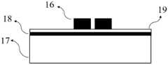
图9为本实施例步骤10的操作示意图;FIG. 9 is an operation schematic diagram of
图10为本实施例步骤12的操作示意图。FIG. 10 is a schematic diagram of the operation of
图中,1、衬底;2、Au薄膜;3、金属薄膜;4、MoS2二维材料层;5、Au层;6、PMMA薄片;7、模具;8、包裹有三明治结构薄膜的环氧树脂;9、超薄切片机;10、包裹有三明治结构薄膜的超薄环氧树脂切片;11、硅片;12、金属电极对;13、隔离层;14、吸收层;15、透光层;16、超短间距金属电极对;17、基片;18、高k栅介质材料;19、MoS2层。In the figure, 1, substrate; 2, Au film; 3, metal film; 4, MoS2 two-dimensional material layer; 5, Au layer; 6, PMMA sheet; 7, mold; 8, ring wrapped with sandwich structure film Oxygen resin; 9. Ultra-thin microtome; 10. Ultra-thin epoxy resin slice wrapped with sandwich structure film; 11. Silicon wafer; 12. Metal electrode pair; 13. Separation layer; 14. Absorbing layer; 15. Light transmission layer; 16, ultra-short pitch metal electrode pair; 17, substrate; 18, high-k gate dielectric material; 19, MoS2 layers.
具体实施方式Detailed ways
为更好的理解本发明,下面的实施例是对本发明的进一步说明,但本发明的内容不仅仅局限于下面的实施例。For better understanding of the present invention, the following examples are further descriptions of the present invention, but the content of the present invention is not limited to the following examples.
本发明中涉及的转移、刻蚀、沉积方式、衬底及基片都是现有技术,不属于本发明的创新点,在此仅做应用。刻蚀方法包括但不限定为氧等离子体刻蚀、氢等离子体刻蚀等。转移包括但不限定为干法转移或湿法转移等。沉积方式包括但不限定为原子层沉积、化学气相沉积、磁控溅射、电子束沉积、脉冲激光沉积、物理气相沉积等。The transfer, etching, deposition methods, substrates and substrates involved in the present invention are all prior art, do not belong to the innovation of the present invention, and are only used here. The etching method includes, but is not limited to, oxygen plasma etching, hydrogen plasma etching, and the like. Transfer includes, but is not limited to, dry transfer or wet transfer, and the like. Deposition methods include but are not limited to atomic layer deposition, chemical vapor deposition, magnetron sputtering, electron beam deposition, pulsed laser deposition, physical vapor deposition, and the like.
(1)将蓝宝石衬底1在丙酮、酒精、去离子水中反复清洗并用氮气烘干;(1) the sapphire substrate 1 is repeatedly cleaned in acetone, alcohol, deionized water and dried with nitrogen gas;
(2)使用物理气相沉积在蓝宝石衬底1的表面依次沉积厚度为100nm的Au薄膜2和厚度约为5nm的Mo金属薄膜3,如图1所示;(2) using physical vapor deposition to sequentially deposit an
(3)将沉积好的Au薄膜2和金属薄膜3放入退火炉中在氩气中退火30min,温度控制在850℃;(3) put the deposited Au
(4)将退火后的样品取出并放置于管式炉中,使薄膜暴露在S蒸汽中10min以形成MoS2二维材料层4;再使用物理气相沉积的方法在MoS2二维材料层4的表面沉积一层Au层5,厚度为100nm,形成Au/MoS2/Au三明治结构的薄膜,如图2所示;(4) The annealed sample is taken out and placed in a tube furnace, and the film is exposed to S steam for 10 min to form a MoS2two -
(5)使用旋涂仪在三明治结构薄膜的表面均匀旋涂PMMA溶液,在150℃的真空环境中烘干;(5) Use a spin coater to uniformly spin-coat the PMMA solution on the surface of the sandwich structure film, and dry in a vacuum environment of 150°C;
(6)将固化好的PMMA从蓝宝石衬底1上揭下,此时三明治结构薄膜转移到PMMA上;(6) the cured PMMA is lifted off from the sapphire substrate 1, and now the sandwich structure film is transferred on the PMMA;
(7)使用金刚石切刀将PMMA和三明治结构薄膜切成宽度为1-2mm的PMMA薄片6,如图3所示;(7) use a diamond cutter to cut PMMA and the sandwich structure film into a
(8)将切下的柔PMMA薄片6置于模具7中并填满环氧树脂将其包裹并固化,得到包裹有三明治结构薄膜的环氧树脂8,如图4和5所示,使用超薄切片机9将包裹有三明治结构薄膜的环氧树脂8切成厚度为20-100nm的包裹有三明治结构薄膜的超薄环氧树脂切片10,如图6所示;(8) Place the cut
(9)将切下的包裹有三明治结构薄膜的超薄环氧树脂切片10转移到硅片11表面,如图7所示,通过刻蚀工艺去除多余的环氧树脂和位于三明治结构中间的MoS2二维材料层4得到金属电极对12,如图8所示;(9) Transfer the cut ultra-thin
(10)对金属电极对12进行干燥处理;待样品干燥后,在它的表面转移厚度为2nm的氮化硼隔离层13、涂覆石墨的厚度为10μm的铝箔吸收层14和透光层15;利用脉宽10ns,波长为1064nm的Nd-YAG激光器所发出的脉冲激光垂直照射透光层15,控制激光通量为17kJ/cm2,照射时间为1s,经过冲击后金属电极对12发生形变,使得它的间距进一步缩小,得到间距为1-5nm的超短间距金属电极对16,如图9所示;(10) Dry the
(11)另取一片干净的硅片基片17,使用原子层沉积的方法在硅片基片17表面沉积厚度为10nm的高k栅介质材料18HfO2,再将CVD方法沉积在SiO2/Si基片上的单层MoS2层19通过PMMA转移到高k栅介质材料18HfO2表面作为晶体管的沟道材料;(11) Take another
(12)将步骤(10)得到的超短间距金属电极对16转移到步骤(11)的MoS2层19表面形成超精细场效应晶体管,如图10所示。(12) Transfer the ultra-short-pitch
以上所述是本发明的优选实施方式而已,当然不能以此来限定本发明之权利范围,应当指出,对于本技术领域的普通技术人员来说,在不脱离本发明原理的前提下,还可以做出若干改进和变动,这些改进和变动也视为本发明的保护范围。The above descriptions are only the preferred embodiments of the present invention, of course, it cannot limit the scope of rights of the present invention. It should be pointed out that for those skilled in the art, without departing from the principles of the present invention, Several improvements and changes are made, and these improvements and changes are also regarded as the protection scope of the present invention.
Claims (10)
Translated fromChinesePriority Applications (1)
| Application Number | Priority Date | Filing Date | Title |
|---|---|---|---|
| CN202010481884.2ACN111627989B (en) | 2020-05-29 | 2020-05-29 | A method of thin-film layers for making ultrafine transistors |
Applications Claiming Priority (1)
| Application Number | Priority Date | Filing Date | Title |
|---|---|---|---|
| CN202010481884.2ACN111627989B (en) | 2020-05-29 | 2020-05-29 | A method of thin-film layers for making ultrafine transistors |
Publications (2)
| Publication Number | Publication Date |
|---|---|
| CN111627989Atrue CN111627989A (en) | 2020-09-04 |
| CN111627989B CN111627989B (en) | 2021-04-02 |
Family
ID=72271359
Family Applications (1)
| Application Number | Title | Priority Date | Filing Date |
|---|---|---|---|
| CN202010481884.2AActiveCN111627989B (en) | 2020-05-29 | 2020-05-29 | A method of thin-film layers for making ultrafine transistors |
Country Status (1)
| Country | Link |
|---|---|
| CN (1) | CN111627989B (en) |
Citations (4)
| Publication number | Priority date | Publication date | Assignee | Title |
|---|---|---|---|---|
| US20170098713A1 (en)* | 2015-10-01 | 2017-04-06 | Zongquan Gu | Engineered Ferroelectric Gate Devices |
| US20170213736A1 (en)* | 2015-03-12 | 2017-07-27 | International Business Machines Corporation | Self-aligned source and drain regions for semiconductor devices |
| CN109411543A (en)* | 2018-09-20 | 2019-03-01 | 华南理工大学 | A kind of transparent film transistor and preparation method thereof |
| CN110164965A (en)* | 2019-04-22 | 2019-08-23 | 中国科学院微电子研究所 | A kind of semiconductor devices and preparation method |
- 2020
- 2020-05-29CNCN202010481884.2Apatent/CN111627989B/enactiveActive
Patent Citations (4)
| Publication number | Priority date | Publication date | Assignee | Title |
|---|---|---|---|---|
| US20170213736A1 (en)* | 2015-03-12 | 2017-07-27 | International Business Machines Corporation | Self-aligned source and drain regions for semiconductor devices |
| US20170098713A1 (en)* | 2015-10-01 | 2017-04-06 | Zongquan Gu | Engineered Ferroelectric Gate Devices |
| CN109411543A (en)* | 2018-09-20 | 2019-03-01 | 华南理工大学 | A kind of transparent film transistor and preparation method thereof |
| CN110164965A (en)* | 2019-04-22 | 2019-08-23 | 中国科学院微电子研究所 | A kind of semiconductor devices and preparation method |
Also Published As
| Publication number | Publication date |
|---|---|
| CN111627989B (en) | 2021-04-02 |
Similar Documents
| Publication | Publication Date | Title |
|---|---|---|
| JP6543461B2 (en) | Wafer dicing using femtosecond laser and plasma etching | |
| CN111628001B (en) | A kind of controllable fabrication method of sub-nano top gate electrode field effect transistor | |
| Chen et al. | Solution-processed metal oxide arrays using femtosecond laser ablation and annealing for thin-film transistors | |
| CN113206005B (en) | Laser fabrication method for tensile strain engineering of 2D materials | |
| CN104538449B (en) | A kind of graphene field effect transistor structure and its extensive manufacture craft | |
| CN107086180B (en) | Preparation method of single nanowire multichannel multiplexing thin film transistor device | |
| Song et al. | High‐resolution van der Waals stencil lithography for 2D transistors | |
| KR20140121137A (en) | Method and board for growing high quality graphene layer using high pressure annealing | |
| CN111987169A (en) | Transistor based on two-dimensional gallium oxide thin film and preparation method | |
| CN105006482B (en) | A kind of preparation method of graphene field effect transistor | |
| CN113206006A (en) | Laser impact preparation method for two-dimensional material tensile strain engineering | |
| CN111627989A (en) | Method for manufacturing ultra-fine transistor by using thin film layer | |
| CN113206004A (en) | Laser impact preparation method for two-dimensional material compressive strain engineering | |
| CN115621322A (en) | Two-dimensional semiconductor material transistor and preparation method thereof | |
| CN103745994A (en) | Field effect transistor by adoption of graphene and preparation method thereof | |
| CN112701156A (en) | Back gate transistor and preparation method thereof | |
| CN104966738B (en) | Active element structure and manufacturing method thereof | |
| CN110634958A (en) | Semiconductor thin film field effect transistor of a kind of unstable two-dimensional material and preparation method thereof | |
| JP7588317B2 (en) | Graphene production method and optical device production method | |
| CN116825827A (en) | Diode with vertical structure of transition metal sulfide and preparation method thereof | |
| CN113823697B (en) | Schottky gate field effect transistor based on two-dimensional size cutting and preparation method thereof | |
| CN111244222B (en) | Hexagonal boron nitride ultraviolet light detector and preparation method thereof | |
| CN111403290B (en) | Method for reducing channel length of field effect transistor by laser shock | |
| CN108231877B (en) | Method for preparing ohmic contact of gallium nitride electronic device | |
| CN107144614B (en) | Preparation method of air nanometer gap electrode |
Legal Events
| Date | Code | Title | Description |
|---|---|---|---|
| PB01 | Publication | ||
| PB01 | Publication | ||
| SE01 | Entry into force of request for substantive examination | ||
| SE01 | Entry into force of request for substantive examination | ||
| GR01 | Patent grant | ||
| GR01 | Patent grant |