CN111615754A - Thermoelectric element - Google Patents
Thermoelectric elementDownload PDFInfo
- Publication number
- CN111615754A CN111615754ACN201980008693.XACN201980008693ACN111615754ACN 111615754 ACN111615754 ACN 111615754ACN 201980008693 ACN201980008693 ACN 201980008693ACN 111615754 ACN111615754 ACN 111615754A
- Authority
- CN
- China
- Prior art keywords
- substrate
- reinforcement
- thermoelectric element
- thermoelectric
- disposed
- Prior art date
- Legal status (The legal status is an assumption and is not a legal conclusion. Google has not performed a legal analysis and makes no representation as to the accuracy of the status listed.)
- Granted
Links
Images


Classifications
- G—PHYSICS
- G02—OPTICS
- G02B—OPTICAL ELEMENTS, SYSTEMS OR APPARATUS
- G02B6/00—Light guides; Structural details of arrangements comprising light guides and other optical elements, e.g. couplings
- G02B6/24—Coupling light guides
- G02B6/42—Coupling light guides with opto-electronic elements
- G02B6/4201—Packages, e.g. shape, construction, internal or external details
- G02B6/4256—Details of housings
- G02B6/4262—Details of housings characterised by the shape of the housing
- G02B6/4265—Details of housings characterised by the shape of the housing of the Butterfly or dual inline package [DIP] type
- H—ELECTRICITY
- H10—SEMICONDUCTOR DEVICES; ELECTRIC SOLID-STATE DEVICES NOT OTHERWISE PROVIDED FOR
- H10N—ELECTRIC SOLID-STATE DEVICES NOT OTHERWISE PROVIDED FOR
- H10N10/00—Thermoelectric devices comprising a junction of dissimilar materials, i.e. devices exhibiting Seebeck or Peltier effects
- H10N10/10—Thermoelectric devices comprising a junction of dissimilar materials, i.e. devices exhibiting Seebeck or Peltier effects operating with only the Peltier or Seebeck effects
- H10N10/17—Thermoelectric devices comprising a junction of dissimilar materials, i.e. devices exhibiting Seebeck or Peltier effects operating with only the Peltier or Seebeck effects characterised by the structure or configuration of the cell or thermocouple forming the device
- G—PHYSICS
- G02—OPTICS
- G02B—OPTICAL ELEMENTS, SYSTEMS OR APPARATUS
- G02B6/00—Light guides; Structural details of arrangements comprising light guides and other optical elements, e.g. couplings
- G02B6/24—Coupling light guides
- G02B6/42—Coupling light guides with opto-electronic elements
- G02B6/4201—Packages, e.g. shape, construction, internal or external details
- G02B6/4266—Thermal aspects, temperature control or temperature monitoring
- G02B6/4268—Cooling
- G02B6/4271—Cooling with thermo electric cooling
- H—ELECTRICITY
- H10—SEMICONDUCTOR DEVICES; ELECTRIC SOLID-STATE DEVICES NOT OTHERWISE PROVIDED FOR
- H10N—ELECTRIC SOLID-STATE DEVICES NOT OTHERWISE PROVIDED FOR
- H10N10/00—Thermoelectric devices comprising a junction of dissimilar materials, i.e. devices exhibiting Seebeck or Peltier effects
- H10N10/01—Manufacture or treatment
- H—ELECTRICITY
- H10—SEMICONDUCTOR DEVICES; ELECTRIC SOLID-STATE DEVICES NOT OTHERWISE PROVIDED FOR
- H10N—ELECTRIC SOLID-STATE DEVICES NOT OTHERWISE PROVIDED FOR
- H10N10/00—Thermoelectric devices comprising a junction of dissimilar materials, i.e. devices exhibiting Seebeck or Peltier effects
- H10N10/80—Constructional details
- H10N10/85—Thermoelectric active materials
- H10N10/851—Thermoelectric active materials comprising inorganic compositions
- H10N10/852—Thermoelectric active materials comprising inorganic compositions comprising tellurium, selenium or sulfur
- H—ELECTRICITY
- H01—ELECTRIC ELEMENTS
- H01S—DEVICES USING THE PROCESS OF LIGHT AMPLIFICATION BY STIMULATED EMISSION OF RADIATION [LASER] TO AMPLIFY OR GENERATE LIGHT; DEVICES USING STIMULATED EMISSION OF ELECTROMAGNETIC RADIATION IN WAVE RANGES OTHER THAN OPTICAL
- H01S5/00—Semiconductor lasers
- H01S5/02—Structural details or components not essential to laser action
- H01S5/022—Mountings; Housings
- H01S5/02208—Mountings; Housings characterised by the shape of the housings
- H01S5/02216—Butterfly-type, i.e. with electrode pins extending horizontally from the housings
- H—ELECTRICITY
- H01—ELECTRIC ELEMENTS
- H01S—DEVICES USING THE PROCESS OF LIGHT AMPLIFICATION BY STIMULATED EMISSION OF RADIATION [LASER] TO AMPLIFY OR GENERATE LIGHT; DEVICES USING STIMULATED EMISSION OF ELECTROMAGNETIC RADIATION IN WAVE RANGES OTHER THAN OPTICAL
- H01S5/00—Semiconductor lasers
- H01S5/02—Structural details or components not essential to laser action
- H01S5/022—Mountings; Housings
- H01S5/0225—Out-coupling of light
- H01S5/02251—Out-coupling of light using optical fibres
- H—ELECTRICITY
- H01—ELECTRIC ELEMENTS
- H01S—DEVICES USING THE PROCESS OF LIGHT AMPLIFICATION BY STIMULATED EMISSION OF RADIATION [LASER] TO AMPLIFY OR GENERATE LIGHT; DEVICES USING STIMULATED EMISSION OF ELECTROMAGNETIC RADIATION IN WAVE RANGES OTHER THAN OPTICAL
- H01S5/00—Semiconductor lasers
- H01S5/02—Structural details or components not essential to laser action
- H01S5/024—Arrangements for thermal management
- H01S5/02407—Active cooling, e.g. the laser temperature is controlled by a thermo-electric cooler or water cooling
- H01S5/02415—Active cooling, e.g. the laser temperature is controlled by a thermo-electric cooler or water cooling by using a thermo-electric cooler [TEC], e.g. Peltier element
Landscapes
- Chemical & Material Sciences (AREA)
- Inorganic Chemistry (AREA)
- Physics & Mathematics (AREA)
- General Physics & Mathematics (AREA)
- Optics & Photonics (AREA)
- Engineering & Computer Science (AREA)
- Manufacturing & Machinery (AREA)
- Cooling Or The Like Of Semiconductors Or Solid State Devices (AREA)
Abstract
Translated fromChinese
Description
Translated fromChinese技术领域technical field
本发明涉及一种热电元件,并且更具体地,涉及一种具有允许防止或显著减少裂纹的发生和衬底的损坏的结构的热电元件。The present invention relates to a thermoelectric element, and more particularly, to a thermoelectric element having a structure that allows the occurrence of cracks and damage to the substrate to be prevented or significantly reduced.
背景技术Background technique
热电效应是由于材料中的电子和空穴的移动而引起的现象,并且意味着在热和电之间的直接能量转换。The thermoelectric effect is a phenomenon caused by the movement of electrons and holes in a material, and means a direct energy conversion between heat and electricity.
热电元件是使用热电效应的装置的通用术语,并且具有其中P型热电材料和N型热电材料被布置在金属电极之间并被结合以形成一对PN结的结构。A thermoelectric element is a general term for a device using the thermoelectric effect, and has a structure in which a P-type thermoelectric material and an N-type thermoelectric material are arranged between metal electrodes and combined to form a pair of PN junctions.
热电元件可以被分类成使用电阻的温度变化的元件、使用其中由于温度差而产生电动势的塞贝克效应的元件和使用珀尔帖效应的元件,珀尔帖效应是由于电流等而发生吸热或散热的现象。Thermoelectric elements can be classified into elements using temperature change of resistance, elements using the Seebeck effect in which an electromotive force is generated due to a temperature difference, and elements using the Peltier effect, which is an endothermic or phenomenon of heat dissipation.
热电元件被广泛应用于家用电器、电子零件和通信零件。例如,热电元件可以被应用于冷却装置、加热装置、发电装置等。因此,对热电元件的热电性能的要求正在逐渐增加。Thermoelectric elements are widely used in household appliances, electronic parts and communication parts. For example, the thermoelectric element can be applied to a cooling device, a heating device, a power generating device, and the like. Therefore, the requirements for thermoelectric performance of thermoelectric elements are gradually increasing.
发明内容SUMMARY OF THE INVENTION
技术问题technical problem
本发明旨在提供一种热电元件,其允许防止或显著减少裂缝的发生和衬底的损坏。The present invention aims to provide a thermoelectric element that allows preventing or significantly reducing the occurrence of cracks and damage to the substrate.
技术方案Technical solutions
本发明的一个方面提供了一种热电元件,该热电元件包括:第一衬底;多个热电支腿,所述多个热电支腿被布置在该第一衬底上;第二衬底,所述第二衬底被布置在第一衬底上的多个热电支腿上;电极,所述电极包括布置在所述第一衬底和多个热电支腿之间的多个第一电极和布置在所述第二衬底和多个热电支腿之间的多个第二电极;和第一增强件,所述第一增强件被布置在第一衬底的侧表面的一部分和下表面上。One aspect of the present invention provides a thermoelectric element comprising: a first substrate; a plurality of thermoelectric legs arranged on the first substrate; a second substrate, the second substrate is disposed on a plurality of thermoelectric legs on the first substrate; an electrode comprising a plurality of first electrodes disposed between the first substrate and the plurality of thermoelectric legs and a plurality of second electrodes disposed between the second substrate and the plurality of thermoelectric legs; and a first reinforcement disposed on and under a portion of the side surface of the first substrate on the surface.
该热电元件可以进一步包括第二增强件,所述第二增强件被布置在第二衬底的侧表面的一部分和上表面上。The thermoelectric element may further include a second reinforcement disposed on a portion of the side surface and the upper surface of the second substrate.
第一增强件可以包括下表面增强件和侧表面增强件,所述下表面增强件被布置在第一衬底的下表面上,所述侧表面增强件从下表面增强件延伸并且被布置在第一衬底的侧表面上。The first reinforcement may include a lower surface reinforcement arranged on the lower surface of the first substrate and a side surface reinforcement extending from the lower surface reinforcement and arranged at the lower surface of the first substrate. on the side surface of the first substrate.
第一衬底的侧表面可以包括长侧表面和短侧表面,并且长侧表面的宽度可以小于或等于布置在长侧表面上的侧表面增强件的总宽度。The side surface of the first substrate may include a long side surface and a short side surface, and a width of the long side surface may be less than or equal to a total width of the side surface reinforcements disposed on the long side surface.
第一衬底的侧表面可以包括短侧表面和长侧表面,并且长侧表面的宽度可以小于或等于布置在长侧表面上的侧表面增强件的总宽度。The side surface of the first substrate may include a short side surface and a long side surface, and the width of the long side surface may be less than or equal to a total width of the side surface reinforcements arranged on the long side surface.
侧表面增强件可以包括第一侧表面增强件和第二侧表面增强件,所述第一侧表面增强件被布置在由第一衬底的短侧表面和长侧表面形成的角部区域中,所述第二侧表面增强件在第一衬底的长侧表面上被布置在沿着宽度方向的中心部分中。The side surface reinforcement may include a first side surface reinforcement and a second side surface reinforcement, the first side surface reinforcement being arranged in a corner region formed by the short side surface and the long side surface of the first substrate , the second side surface enhancer is arranged in a central portion in the width direction on the long side surface of the first substrate.
下表面增强件可以包括:第一层,该第一层被布置在第一衬底的下表面上;第二层,该第二层被布置在第一层上;和第三层,该第三层被布置在第二层上,并且侧表面增强件可以由下表面增强件的第一层形成。The lower surface enhancer may include: a first layer disposed on the lower surface of the first substrate; a second layer disposed on the first layer; and a third layer The three layers are arranged on the second layer, and the side surface reinforcement may be formed from the first layer of the lower surface reinforcement.
第一层可以由铜制成,第二层可以由镍制成,并且第三层可以由金制成。The first layer may be made of copper, the second layer may be made of nickel, and the third layer may be made of gold.
第一增强件的高度可以是第一衬底的高度的0.2到1.5倍。The height of the first reinforcement may be 0.2 to 1.5 times the height of the first substrate.
第一增强件可以包括上表面增强件,所述上表面增强件从侧表面增强件延伸并被布置在第一衬底的上表面上,并且所述上表面增强件可以与所述多个热电支腿和电极隔开。The first reinforcement may include an upper surface reinforcement extending from the side surface reinforcement and disposed on the upper surface of the first substrate, and the upper surface reinforcement may be associated with the plurality of thermoelectrics The legs are separated from the electrodes.
该热电元件可以进一步包括绝缘部件,所述绝缘部件被布置在上表面增强件和电极之间。The thermoelectric element may further include an insulating member disposed between the upper surface reinforcement and the electrode.
有利的效果favorable effect
根据本发明的实施例,能够提供具有优异性能的热电元件。According to the embodiments of the present invention, a thermoelectric element having excellent performance can be provided.
特别地,根据本发明的实施例,能够防止或显著减少裂缝的产生和衬底的损坏。In particular, according to the embodiments of the present invention, the generation of cracks and the damage of the substrate can be prevented or significantly reduced.
另外,根据本发明的实施例,能够提供具有改进的热传递效率的热电元件。In addition, according to the embodiments of the present invention, a thermoelectric element having improved heat transfer efficiency can be provided.
附图说明Description of drawings
图1是示意根据本发明的一个实施例的热电元件的透视图。FIG. 1 is a perspective view illustrating a thermoelectric element according to an embodiment of the present invention.
图2是示意根据本发明的一个实施例的热电元件的侧视图。2 is a side view illustrating a thermoelectric element according to an embodiment of the present invention.
图3是沿图2的线A-A截取的截面视图。FIG. 3 is a cross-sectional view taken along line A-A of FIG. 2 .
图4是图2的部分4的放大视图。FIG. 4 is an enlarged view of part 4 of FIG. 2 .
图5是示意根据本发明的另一个实施例的热电元件的侧视图。5 is a side view illustrating a thermoelectric element according to another embodiment of the present invention.
图6是沿图5的线B-B截取的截面视图。FIG. 6 is a cross-sectional view taken along line B-B of FIG. 5 .
图7是示意根据本发明的又一个实施例的热电元件的截面视图。7 is a cross-sectional view illustrating a thermoelectric element according to still another embodiment of the present invention.
图8是沿图7的线C-C截取的截面视图。FIG. 8 is a cross-sectional view taken along line C-C of FIG. 7 .
图9是示意根据本发明的再一个实施例的热电元件的侧视图。9 is a side view illustrating a thermoelectric element according to still another embodiment of the present invention.
图10是沿图9的线D-D截取的截面视图。FIG. 10 is a cross-sectional view taken along line D-D of FIG. 9 .
图11到图13是示意根据本发明的实施例的热电元件的热电支腿的示例的图。11 to 13 are diagrams illustrating examples of thermoelectric legs of a thermoelectric element according to an embodiment of the present invention.
图14是示出根据本发明的实施例的热电元件被应用于此的蝶型激光二极管(LD)模块的透视图。14 is a perspective view illustrating a butterfly laser diode (LD) module to which a thermoelectric element according to an embodiment of the present invention is applied.
具体实施方式Detailed ways
本发明可以被变型为各种形式并且可以具有各种实施例,并且因此,将在附图中示意并描述特定实施例。然而,不应以将本发明限制于特定实施例的意义来理解实施例,而应将其解释为包括在本发明的精神和技术范围内的变型、等同或替代。The present invention may be modified in various forms and may have various embodiments, and therefore, specific embodiments will be illustrated and described in the accompanying drawings. However, the embodiments should not be construed in the sense of limiting the present invention to the specific embodiments, but should be construed as including modifications, equivalents, or substitutions within the spirit and technical scope of the present invention.
本文中使用的包括序数(诸如第一、第二等)的术语可以用于描述各种构件,但是所述各种构件不受这些术语限制。这些术语仅用于将一个构件与另一个构件区分开的目的。例如,在不脱离本发明的范围的情况下,第二构件可以被称为第一构件,并且类似地,第一构件也可以被称为第二构件。术语“和/或”包括多个相关的列出项目的组合或所述多个相关的列出项目中的任一项。Terms including ordinal numbers (such as first, second, etc.) used herein may be used to describe various components, but the various components are not limited by these terms. These terms are only used for the purpose of distinguishing one element from another. For example, a second member could be termed a first member, and, similarly, a first member could be termed a second member, without departing from the scope of the present invention. The term "and/or" includes combinations of or any of the plurality of associated listed items.
当一个构件被称为“连接”或“联接”到另一个构件时,它可以被直接连接或联接到另一个构件,但是应该理解,又一个构件可能存在于该构件和另一个构件之间。相反,当构件被称为“直接连接”或“直接联接”到另一个构件时,应当理解,在该构件和另一个构件之间可以不存在又一个构件。When a member is referred to as being "connected" or "coupled" to another member, it can be directly connected or coupled to the other member, but it will be understood that another member may exist between the member and the other member. In contrast, when a member is referred to as being "directly connected" or "directly coupled" to another member, it will be understood that the other member may not be present between the member and the other member.
本文中所使用的术语仅被采用为描述特定实施例,而非旨在限制本发明。除非上下文另外明确指出,否则单数形式包括复数形式。应当理解,术语“包括”、“包含”和“具有”指定在这里描述的特征、数目、步骤、操作、构件、元件或其组合的存在,但不排除存在或添加一个或多个其它特征、数目、步骤、操作、构件、元件或其组合的可能性。The terminology used herein is employed to describe particular embodiments only, and is not intended to limit the present invention. The singular includes the plural unless the context clearly dictates otherwise. It should be understood that the terms "comprising", "comprising" and "having" designate the presence of features, numbers, steps, operations, components, elements or combinations thereof described herein, but do not preclude the presence or addition of one or more other features, Possibilities of numbers, steps, operations, components, elements, or combinations thereof.
除非另有定义,否则本文中所使用的包括技术术语或科学术语的所有术语具有与本发明所属领域的技术人员通常理解的含义相同的含义。在字典中定义的通用术语应被解释为具有在相关技术的上下文中一致的含义,并且除非在本申请中明确定义,否则不应被解释为具有理想的或过分形式化的含义。Unless otherwise defined, all terms including technical or scientific terms used herein have the same meaning as commonly understood by one of ordinary skill in the art to which this invention belongs. Generic terms defined in dictionaries should be construed as having meanings consistent in the context of the related art, and should not be construed as having ideal or overly formalized meanings unless explicitly defined in this application.
在下文中,将参考附图详细描述本发明的实施例,相同的附图标记被赋予相同的构件或对应的构件,而与绘图编号无关,并且将省略其重复描述。Hereinafter, the embodiments of the present invention will be described in detail with reference to the accompanying drawings, the same reference numerals are assigned to the same members or corresponding members regardless of drawing numbers, and repeated descriptions thereof will be omitted.
图1是示意根据本发明的一个实施例的热电元件的透视图,图2是示意根据本发明的一个实施例的热电元件的侧视图,图3是沿图2的线A-A截取的截面视图,并且图4是图2的部分4的放大视图。1 is a perspective view illustrating a thermoelectric element according to an embodiment of the present invention, FIG. 2 is a side view illustrating a thermoelectric element according to an embodiment of the present invention, and FIG. 3 is a cross-sectional view taken along line A-A of FIG. 2 , And FIG. 4 is an enlarged view of part 4 of FIG. 2 .
参考图1到图4,根据本发明的一个实施例的热电元件100包括P型热电支腿120、N型热电支腿130、下衬底140、上衬底150、增强件170、电极160和引线180。1 to 4 , a
电极160包括第一电极161和第二电极162,引线180包括连接到第一电极161的第一引线181和连接到第二电极162的第二引线182。The
下电极161被布置在下衬底140与P型热电支腿120和N型热电支腿130的下底表面之间,并且上电极162被布置在上衬底150与P型热电支腿120和N型热电支腿130的下底表面之间。因此,多个P型热电支腿120和多个N型热电支腿130通过下电极161和上电极162电连接。布置在下电极161和上电极162之间并且彼此电连接的一对P型热电支腿120和N型热电支腿130可以形成单元电池。The
例如,当通过第一引线181和第二引线182将电压施加到下电极161和上电极162时,由于珀尔帖效应而导致的电流在其中从P型热电支腿120流向N型热电支腿130的衬底可以吸收热量以用作吸热部,并且电流在其中从N型热电支腿130流向P型热电支腿120的衬底可以被加热以用作散热部。For example, when a voltage is applied to the
这里,所述P型热电支腿120和N型热电支腿130中的每一个热电支腿可以是包含Bi和Te作为主要原材料的碲化铋(Bi-Te)基热电支腿。100重量%的P型热电支腿120可以是包括99到99.999重量%的Bi-Te基主要原材料(main low material)并且包括0.001到1重量%的包含Bi或Te的混合物的热电支腿,该Bi-Te基主要原材料包含锑(Sb)、镍(Ni)、Al、Cu、银(Ag)、铅(Pb)、硼(B)、镓(Ga)、Te、Bi和铟(In)中的至少一种。例如,100重量%的P型热电支腿120可以包括Bi-Se-Te作为主要原材料,并且可以进一步包括0.001到1wt%的Bi或Te。100重量%的N型热电支腿130可以是包括99到99.999wt%的Bi-Te基原材料(lowmaterial)并且包括0.001到1wt%的包含Bi或Te的混合物的热电支腿,该Bi-Te基原材料包含硒(Se)、Ni、Al、Cu、Ag、Pb、B、Ga、Te、Bi和In中的至少一种。例如,100重量%的N型热电支腿130可以包括Bi-Sb-Te作为主要原材料,并且可以进一步包括0.001到1wt%的Bi或Te。Here, each of the P-type
所述P型热电支腿120和N型热电支腿130中的每一个热电支腿可以被形成为块状形状或堆叠形状。通常,可以通过以下方式来获得块形的P型热电支腿120或块形的N型热电支腿130:对热电材料进行热处理以生产锭块,粉碎并筛分该锭块以获得热电支腿粉末,烧结热电支腿粉末并切割该烧结体。可以通过如下方式来获得堆叠形的P型热电支腿120或堆叠形的N型热电支腿130:将包含热电材料的糊剂涂敷在片形衬底上以形成单元部件、堆叠单元部件并切割堆叠的单元部件。Each of the P-type
在这种情况下,该一对P型热电支腿120和N型热电支腿130可以具有相同的形状和高度或者可以具有不同的形状和体积。例如,由于P型热电支腿120和N型热电支腿130的电导率特性不同,所以N型热电支腿130的截面面积可以与P型热电支腿120的截面面积不同地形成。In this case, the pair of P-type
根据本发明的一个实施例的热电元件的性能可以由热电优值ZT表示。热电优值ZT可以用公式1表达。The performance of a thermoelectric element according to an embodiment of the present invention may be represented by a thermoelectric figure of merit ZT. The thermoelectric figure of merit ZT can be expressed by Equation 1.
[公式1][Formula 1]
ZT=α2σT/kZT=α2 σT/k
这里,α为塞贝克系数(V/K),σ为电导率(S/m),并且α2σ为功率因数(W/mK2)。此外,T是温度,并且k是导热率(W/mK)。k可以被表达为a·cp·ρ,a是热扩散率(cm2/S),cp是比热(J/gK),并且ρ是密度(g/cm3)。Here, α is the Seebeck coefficient (V/K), σ is the electrical conductivity (S/m), and α2 σ is the power factor (W/mK2 ). Furthermore, T is temperature, and k is thermal conductivity (W/mK). k can be expressed as a·cp·ρ , where a is the thermal diffusivity (cm2 /S), cp is the specific heat (J/gK), andρ is the density (g/cm3 ).
为了获得热电元件的优值ZT,使用Z计来测量Z值(V/K),并且可以使用所测量的Z值来计算优值ZT。In order to obtain the figure of merit ZT of the thermoelectric element, the Z value (V/K) is measured using a Z meter, and the figure of merit ZT can be calculated using the measured Z value.
这里,布置在下衬底140、P型热电支腿120和N型热电支腿130之间的下电极120,以及布置在上衬底150、P型热电支腿120和N型热电支腿130之间的上电极162可以各自包括Cu、Ag和Ni中的至少一种。Here, the
另外,彼此相反的下衬底140和上衬底150可以是绝缘衬底或金属衬底。绝缘衬底可以是具有挠性的氧化铝衬底或聚合物树脂衬底。具有挠性的聚合物树脂衬底可以包括各种绝缘树脂材料,诸如高渗透性塑料等,诸如聚酰亚胺(PI)、聚苯乙烯(PS)、聚甲基丙烯酸甲酯(PMMA)、环烯烃共聚物(COC)、聚对苯二甲酸乙二醇酯(PET)和树脂。替代地,绝缘衬底可以是织物。金属衬底可以包括Cu、Cu合金或Cu-Al合金。另外,当下衬底140和上衬底150是金属衬底时,介电层可以进一步被形成在在下衬底140和下电极161之间并且在上衬底150和上电极162之间。介电层可以包括具有范围从5到10W/mK的导热率的材料。In addition, the
在这种情况下,下衬底140和上衬底150的尺寸可以被形成为彼此不同。例如,所述下衬底140和上衬底150中的一个衬底的体积、厚度或面积可以被形成为大于另一个衬底的体积、厚度或面积。因此,可以提高热电元件的吸热性能或散热性能。In this case, the sizes of the
所述多个下电极161和多个上电极162可以各自以m×n阵列的形式布置(这里,m和n中的每一个可以是一或更大的整数,并且m和n可以彼此相同或彼此不同),但是本发明不限于此。下电极161和上电极162可以各自被布置成从与其相邻的另一个下电极161和另一个上电极162隔开。例如,下电极161和上电极162可以被布置成从与其相邻的另一个下电极161和另一个上电极262间隔大约0.5mm到0.8mm。The plurality of
另外,一对P型热电支腿120和N型热电支腿130被布置在下电极161上,并且该一对P型热电支腿120和N型热电支腿130被布置在上电极162下方。In addition, a pair of P-type
即,P型热电支腿120的底表面可以被布置在下电极161上,并且其顶表面可以被布置在上电极162上,并且N型热电支腿130的底表面可以被布置在下电极161上,并且其顶表面可以被布置在上电极162上。当布置在下电极161上的该一对P型热电支腿120和N型热电支腿130中的P型热电支腿120被布置在所述多个下电极162中的一个下电极161上时,N型热电支腿130可以被布置在与该一个下电极161相邻的另一个下电极162上。因此,所述多个P型热电支腿120和多个N型热电支腿130通过下电极161和下电极162以串联方式电连接。That is, the bottom surface of the P-type
在这种情况下,一对下焊料层可以被涂敷在下电极161上,以结合该一对P型热电支腿120和N型热电支腿130,并且该一对P型热电支腿120和N型热电支腿130可以被布置在该一对下焊料层上。In this case, a pair of lower solder layers may be coated on the
增强件170包括布置在下衬底140下方的下增强件171和布置在上衬底150下方的上增强件172。The
这里,增强件170可以通过诸如电镀或热喷涂的工艺被布置在下衬底140和上衬底150上。Here, the
同时,下衬底140可以具有矩形形状,并且可以包括面向彼此的一对短侧表面141和面向彼此的一对长侧表面142。Meanwhile, the
这里,所述长侧表面142中的每一个长侧表面具有第一宽度W1。Here, each of the long side surfaces 142 has a first width W1.
下增强件171可以包括布置在下衬底140的下表面上的下表面增强件171a和布置在下衬底140的短侧表面141和长侧表面142上的侧表面增强件171b。The
这里,上增强件172还可以包括布置在上衬底150的上表面上的上表面增强件和布置在上衬底150的短侧表面和长侧表面上的侧表面增强件。Here, the
然而,在下文中,将通过布置在下衬底140上的下增强件171来描述本发明的一个实施例。However, in the following, an embodiment of the present invention will be described by the
下增强件171的侧表面增强件171b的高度T2可以小于或等于下衬底140的高度T1。The height T2 of the
同时,下增强件171的侧表面增强件171b的高度T2可以被形成为下衬底140的高度T1的0.2到1.5倍。Meanwhile, the height T2 of the
这里,当下增强件171的侧表面增强件171b的高度T2小于下衬底140的高度T1的0.2倍时,不能抑制传递到下衬底140的外力。当下增强件171的侧表面增强件171b的高度T2超过下衬底140的高度T1的1.5倍时,形成侧表面增强件171b是不必要的,并且因此P型热电支腿120和N型热电支腿130可能不必要地与侧表面增强件171b接触,使得在P型热电支腿120和N型热电支腿130之间可能发生电短路。Here, when the height T2 of the
另外,优选的是,下增强件171的侧表面增强件171b的高度T2被形成为下衬底140的高度T1的0.2到1倍。此外,更优选的是,下增强件171的侧表面增强件171b的高度T2被形成为下衬底140的高度T1的0.2倍到0.8倍。In addition, it is preferable that the height T2 of the
此外,下增强件171的侧表面增强件171b的宽度W2可以大于或等于下衬底140的长侧表面142的宽度W1。In addition, the width W2 of the
即,侧表面增强件171b可以在宽度方向上完全覆盖下衬底140的长侧表面142。这里,侧表面增强件171b完全覆盖下衬底140的长侧表面142可以意味着,基于相同的高度,侧表面增强件171b在宽度方向上被布置在下衬底140的整个长侧表面142上。That is, the
同时,参考图4,下表面增强件171a可以包括多个金属层。Meanwhile, referring to FIG. 4 , the
所述多个金属层包括第一层11、第二层12和第三层13。The plurality of metal layers include a
第一层11可以被布置在下衬底140的下表面上,并且可以包括经济并且有利于形成厚度的第一金属。The
第二层12可以被布置在第一层11上,并且可以包括改善在第一层11和第三层13之间的附着的第二金属。The
第三层13可以被布置在第二层12上,并且可以包括抗氧化性优异并且易于结合到外部装置的第三金属。The
例如,第一金属可以包括Cu,第二金属可以包括Ni,并且第三金属可以包括金。For example, the first metal may include Cu, the second metal may include Ni, and the third metal may include gold.
这里,第一层11可以在所述多个金属层中占据约95%的体积,第二层12可以在其中占据约10%的体积,并且第三层13可以在其中占据约1%的体积。Here, the
同时,侧表面增强件171b可以仅由第一层形成,该第一层不被结合到外部装置,并且由诸如Cu的第一金属制成,使得与下衬底140的热交换优异。Meanwhile, the
在下文中,将参考图5和6描述根据本发明的另一个实施例的热电元件。Hereinafter, a thermoelectric element according to another embodiment of the present invention will be described with reference to FIGS. 5 and 6 .
图5是示意根据本发明的另一个实施例的热电元件的侧视图,并且图6是沿图5的线B-B截取的截面视图。5 is a side view illustrating a thermoelectric element according to another embodiment of the present invention, and FIG. 6 is a cross-sectional view taken along line B-B of FIG. 5 .
参考图5和图6,当与图2所示的根据本发明的一个实施例的热电元件相比时,根据本发明另一个实施例的热电元件具有增强件270的不同配置。因此,在下文中,将仅详细描述增强件270的不同配置,并且在此将省略具有重叠的附图标记的相同构件的详细描述。Referring to FIGS. 5 and 6 , a thermoelectric element according to another embodiment of the present invention has a different configuration of reinforcements 270 when compared to the thermoelectric element according to one embodiment of the present invention shown in FIG. 2 . Therefore, hereinafter, only the different configurations of the reinforcement 270 will be described in detail, and the detailed description of the same components with overlapping reference numerals will be omitted here.
增强件270包括布置在下衬底140下方的下增强件271和布置在上衬底150下方的上增强件272。The reinforcements 270 include
这里,增强件270可以通过诸如电镀或热喷涂的工艺布置在下衬底140和上衬底150上。Here, the reinforcements 270 may be arranged on the
下增强件271包括布置在下衬底140的下表面上的下表面增强件271a,和布置在下衬底140的短侧表面141和长侧表面142上的侧表面增强件271b。The
这里,上增强件272还可以包括布置在上衬底150的上表面上的上表面增强件和布置在上衬底150的短侧表面和长侧表面上的侧表面增强件。Here, the
然而,在下文中,将通过布置在下衬底140上的下增强件271来描述本发明的另一个实施例。However, in the following, another embodiment of the present invention will be described by the
下增强件271的侧表面增强件271b的高度T2可以小于或等于下衬底140的高度T1。The height T2 of the
同时,下增强件271的侧表面增强件271b的高度T2可以被形成为下衬底140的高度T1的0.2到1.5倍。Meanwhile, the height T2 of the
这里,当下增强件271的侧表面增强件271b的高度T2小于下衬底140的高度T1的0.2倍时,不能抑制传递到下衬底140的外力。当下增强件271的侧表面增强件271b的高度T2超过下衬底140的高度T1的1.5倍时,形成侧表面增强件271b是不必要的,并且因此P型热电支腿120和N型热电支腿130可能不必要地与侧表面增强件271b接触,使得在P型热电支腿120和N型热电支腿130之间可能发生电短路。Here, when the height T2 of the
另外,优选的是,下增强件271的侧表面增强件271b的高度T2被形成为下衬底140的高度T1的0.2到1倍。更优选的是,下增强件271的侧表面增强件271b的高度T2被形成为下衬底140的高度T1的0.2倍到0.8倍。In addition, it is preferable that the height T2 of the
同时,下增强件271的侧表面增强件271b包括第一侧表面增强件271b'和第二侧表面增强件271b″。Meanwhile, the
第一侧表面增强件271b'被布置在由下衬底140的长侧表面142和短侧表面141形成的角部区域140a中。这里,第一侧表面增强件271b'在角部区域140a中被布置在长侧表面142和短侧表面141的一部分上并且具有大致
第二侧表面增强件271b″被布置在具有在宽度方向上从下衬底140的长侧表面142的中心CL到一侧和另一侧的预定范围的中心部分中。The second
这里,侧表面增强件271b具有第一侧表面增强件271b'的宽度W31和W33与第二侧表面增强件271b″的宽度W32作为在宽度方向上的总宽度W3。Here, the
同时,由于第一侧表面增强件271b'被布置成与第二侧表面增强件271b″隔开,所以侧表面增强件271b的总宽度W3可以小于下衬底140的长侧表面142的宽度W1。Meanwhile, since the first
即,除了长侧表面142在宽度方向上的一部分之外,侧表面增强件271b可以覆盖下衬底140的长侧表面142。That is, the
在下文中,将参考图7和8描述根据本发明的又一个实施例的热电元件。Hereinafter, a thermoelectric element according to still another embodiment of the present invention will be described with reference to FIGS. 7 and 8 .
图7是示意根据本发明的又一个实施例的热电元件的截面视图,并且图8是沿图7的线C-C截取的截面视图。7 is a cross-sectional view illustrating a thermoelectric element according to still another embodiment of the present invention, and FIG. 8 is a cross-sectional view taken along line C-C of FIG. 7 .
参考图7和图8,当与图2所示的根据本发明的一个实施例的热电元件相比时,根据本发明的又一个实施例的热电元件具有增强件370的不同配置。因此,在下文中,将仅详细描述增强件370的不同配置,并且在此将省略具有重叠的附图标记的相同构件的详细描述。Referring to FIGS. 7 and 8 , a thermoelectric element according to yet another embodiment of the present invention has a different configuration of reinforcements 370 when compared to the thermoelectric element according to one embodiment of the present invention shown in FIG. 2 . Therefore, hereinafter, only the different configurations of the reinforcing member 370 will be described in detail, and the detailed description of the same components with overlapping reference numerals will be omitted here.
增强件370包括布置在下衬底140下方的下增强件371和布置在上衬底150下方的上增强件372。The reinforcements 370 include
这里,增强件370可以通过诸如电镀或热喷涂的工艺被布置在下衬底140和上衬底150上。Here, the reinforcements 370 may be arranged on the
下增强件371包括布置在下衬底140的下表面上的下表面增强件371a和布置在下衬底140的短侧表面141和长侧表面142上的侧表面增强件371b。The
这里,上增强件372还可以包括布置在上衬底150的上表面上的上表面增强件和布置在上衬底150的短侧表面和长侧表面上的侧表面增强件。Here, the
然而,在下文中,将通过布置在下衬底140上的下增强件371来描述本发明的又一个实施例。However, in the following, still another embodiment of the present invention will be described by the
下增强件371的侧表面增强件371b的高度T3可以大于下衬底140的高度T1,并且下衬底140的上表面可以与侧表面增强件371b的上表面共面。The height T3 of the
即,侧表面增强件371b可以在宽度方向和高度方向上完全覆盖下衬底140的长侧表面142。这里,这意味着侧表面增强件371b被布置在下衬底140的长侧表面142的所有侧表面上。That is, the
同时,优选的是,下增强件371的侧表面增强件371b与P型热电支腿120、N型热电支腿130、第一电极161、第二电极162、第一引线181和第二引线182隔开并且不与其接触,或者在它们之间布置绝缘部件(未示出)。Meanwhile, it is preferable that the
即,在根据本发明的又一个实施例的热电元件中,由于下增强件371被布置成围绕下衬底140的所有下表面和侧表面,所以可以防止下衬底140由于外力而变形和损坏。That is, in the thermoelectric element according to still another embodiment of the present invention, since the
在下文中,将参考图9和10描述根据本发明的再一个实施例的热电元件。Hereinafter, a thermoelectric element according to still another embodiment of the present invention will be described with reference to FIGS. 9 and 10 .
图9是示意根据本发明的再一个实施例的热电元件的侧视图,并且图10是沿图9的线D-D截取的截面视图。9 is a side view illustrating a thermoelectric element according to still another embodiment of the present invention, and FIG. 10 is a cross-sectional view taken along line D-D of FIG. 9 .
参考图9和图10,当与图2所示的根据本发明的一个实施例的热电元件相比时,根据本发明的再一个实施例的热电元件具有增强件470的不同配置。因此,在下文中,将仅详细描述增强件470的不同配置,并且在此将省略具有重叠的附图标记的相同构件的详细描述。Referring to FIGS. 9 and 10 , a thermoelectric element according to yet another embodiment of the present invention has a different configuration of reinforcements 470 when compared to the thermoelectric element according to one embodiment of the present invention shown in FIG. 2 . Therefore, hereinafter, only the different configurations of the reinforcement member 470 will be described in detail, and the detailed description of the same components with overlapping reference numerals will be omitted here.
增强件470包括布置在下衬底140下方的下增强件471和布置在上衬底150下方的上增强件472。The reinforcements 470 include
这里,增强件470可以通过诸如电镀或热喷涂的工艺被布置在下衬底140和上衬底150上。Here, the reinforcements 470 may be disposed on the
下增强件471包括布置在下衬底140的下表面上的下表面增强件471a、布置在下衬底140的短侧表面141和长侧表面142上的侧表面增强件471b和布置在下衬底140的上表面的一部分上的上表面增强件471c。The
这里,上增强件472还可以包括布置在上衬底150的上表面上的上表面增强件、布置在上衬底150的短侧表面和长侧表面上的侧表面增强件和布置在上衬底150的下表面的一部分上的下表面增强件。Here, the
然而,在下文中,将通过布置在下衬底140上的下增强件471来描述本发明的再一个实施例。However, in the following, still another embodiment of the present invention will be described by the
下增强件471的侧表面增强件471b的高度T4可以大于下衬底140的高度T1,并且侧表面增强件471b的上表面可以被布置在比下衬底140的上表面更高的水平面处。The height T4 of the
即,侧表面增强件471b可以在宽度方向和高度方向上完全覆盖下衬底140的长侧表面142。这里,这意味着侧表面增强件471b被布置在下衬底140的长侧表面142的所有侧表面上。That is, the
上表面增强件471c可以从侧表面增强件471b的端部延伸并且覆盖下衬底140的上表面的一部分。这里,优选的是,下增强件471的上表面增强件471c与P型热电支腿120、N型热电支腿130、第一电极161、第二电极162、第一引线181和第二引线182隔开并且不与它们接触,或者在它们之间布置绝缘部件(未示出)。The
即,在根据本发明的再一个实施例的热电元件中,由于下增强件471被布置成包围下衬底140的所有的下表面、侧表面和上表面的一部分,因此,可以防止下衬底140由于外力而变形和损坏。That is, in the thermoelectric element according to still another embodiment of the present invention, since the
在下文中,将参考图11到13描述根据本发明的实施例的热电元件的热电支腿的示例。Hereinafter, an example of a thermoelectric leg of a thermoelectric element according to an embodiment of the present invention will be described with reference to FIGS. 11 to 13 .
图11到图13是示意根据本发明的另一个实施例的热电元件的热电支腿的示例的图。11 to 13 are diagrams illustrating examples of thermoelectric legs of a thermoelectric element according to another embodiment of the present invention.
在本发明的另一个实施例中,上述热电支腿的结构可以被实现为具有堆叠结构而不是块状结构的结构,从而进一步改进薄度和冷却效率。In another embodiment of the present invention, the structure of the thermoelectric legs described above may be implemented as a structure having a stacked structure instead of a block structure, thereby further improving the thinness and cooling efficiency.
具体地,图11中的P型热电支腿120和N型热电支腿中的每一个热电支腿的结构都被形成为使得多个结构被堆叠以形成单元部件,并且然后切割该单元部件,所述结构中的每一个结构通过将半导体材料涂敷在片形衬底上而被形成。因此,能够防止材料损失并改进导电特性。Specifically, the structure of each of the P-type
在这方面,参考图11,图11示意制造具有上述堆叠结构的单元部件的处理的概念图表。In this regard, reference is made to FIG. 11 , which illustrates a conceptual diagram of the process of manufacturing a unit component having the above-described stack structure.
参考图11,以糊剂的形式制备包括半导体材料的材料,并将该糊剂涂敷在诸如片材、膜等的基础衬底1110上,以形成半导体层1120,从而形成了一个单元部件1100。如图11中所示,通过堆叠多个单元部件1100a、1100b和1100c来将单元部件1100形成为堆叠结构,并且然后该堆叠结构被切割以形成单元热电元件1200。即,根据本发明的单元热电元件1200可以以其中堆叠了多个单元部件1100的结构形成,在所述单元部件的每一个单元部件中,半导体层1120被堆叠在基础衬底1110上。Referring to FIG. 11 , a material including a semiconductor material is prepared in the form of a paste, and the paste is applied on a
在上述处理中,在基础衬底1110上涂敷半导体糊剂可以使用各种方法来实现。例如,可以通过流延成型(即,通过将非常细的半导体材料粉末与水性溶剂或非水性溶剂和选自结合剂、增塑剂、分散剂、消泡剂和表面活性剂中的任何一种混合以制备浆料,并且然后以预定厚度在根据目的的移动刀片或移动载体衬底上形成浆料的工艺)来实现半导体糊剂的涂敷。在这种情况下,可以将厚度在10μm到100μm的范围中的诸如膜、片材等的材料用作基础衬底,并且用于形成上述块型元件的P型材料和N型材料也可以作为正被涂敷的半导体材料被直接地涂敷。In the above-described process, the coating of the semiconductor paste on the
单元部件1100可以通过以多层布置和堆叠单元部件1100的处理来在范围从50℃到250℃的温度下被压缩而形成为堆叠结构。在本发明的实施例中,堆叠的单元部件1100的数目的范围可以从两个到五十个。The
此后,可以以期望的形状和尺寸执行切割处理,并且可以添加烧结处理。After that, a cutting process can be performed in a desired shape and size, and a sintering process can be added.
通过堆叠根据上述工艺制造的多个单元部件1100而形成的单元热电元件可以确保厚度、形状和尺寸的均匀性。即,现有的块形热电元件是通过如下方式制造的:将锭块粉碎、将所粉碎的锭块进行微球磨并切割烧结的块状结构。因此,存在以下问题,由于范围从3mm到5mm的较厚的厚度,损失了大量的材料,难以切割成均匀的尺寸,并且难以实现薄型化。具有根据本发明的实施例的堆叠结构的单元热电元件是通过将片形的单元部件堆叠为多层并切割该片形的堆叠结构来制造的。因此,材料几乎不损失并且具有均匀的厚度,使得可以确保材料的均匀性,可以将整个单元热电元件的厚度减小到1.5mm或更小以实现薄型化,并且单元热电元件可以采用各种形状。与根据图1中的本发明的一个实施例的上述热电支腿的结构相同,可以通过切割成规则的六面体结构或长方体结构来实现最终实现的结构。The unit thermoelectric element formed by stacking the plurality of
特别地,在根据本发明的另一个实施例的单元热电元件的制造处理中,在形成单元部件1100的堆叠结构的处理中,制造处理可以被实现为进一步包括在每个单元部件1100的表面上形成导电层的处理。In particular, in the manufacturing process of the unit thermoelectric element according to another embodiment of the present invention, in the process of forming the stacked structure of the
即,可以在图11C中的堆叠结构的单元部件之间形成具有图12的结构的导电层。导电层可以被形成在与基础衬底的、在其上形成半导体层的表面相反的表面上。在这种情况下,导电层可以被形成为图案层,以形成露出单元部件的表面的区域。当与在基础衬底的整个表面上涂敷导电层的情况相比时,能够实现增加电导率、提高在单元部件之间的附着强度并且降低导热率的优点。That is, a conductive layer having the structure of FIG. 12 may be formed between the unit components of the stacked structure in FIG. 11C . The conductive layer may be formed on a surface opposite to the surface of the base substrate on which the semiconductor layer is formed. In this case, the conductive layer may be formed as a pattern layer to form a region where the surface of the unit part is exposed. When compared with the case where the conductive layer is applied on the entire surface of the base substrate, the advantages of increasing the electrical conductivity, improving the adhesion strength between unit parts, and reducing the thermal conductivity can be achieved.
即,图12示意根据本发明实施例的导电层C的各种变型示例。可以通过将其不同地修改为包括如图12A和图12B中所示的封闭型开口图案c1和c2的网型结构或者包括如图12C和图12D中所示敞开型开口图案c3和c4的线型来设计单元部件的表面被露出的图案。如上所述,导电层实现以下优点:改进在由单元部件的堆叠结构形成的单元热电元件中的单元部件之间的附着强度,减小在单元部件之间的导热率,并且提高电导率。因此,当与传统的块型热电元件相比时,冷却能力Qc和ΔT改进,并且特别地,功率因数增加1.5倍,即,电导率增加1.5倍。电导率的增加与热电效率的改进直接相关,使得冷却效率被提高。导电层可以由金属材料形成,并且可以应用诸如Cu、Ag、Ni等的所有基于金属的电极材料。That is, FIG. 12 illustrates various modified examples of the conductive layer C according to the embodiment of the present invention. It can be variously modified into a mesh structure including closed-type opening patterns c1 and c2 as shown in FIGS. 12A and 12B or a line including open-type opening patterns c3 and c4 as shown in FIGS. 12C and 12D pattern to design the pattern in which the surface of the unit part is exposed. As described above, the conductive layer achieves the advantages of improving adhesion strength between unit components in a unit thermoelectric element formed by a stacked structure of unit components, reducing thermal conductivity between unit components, and increasing electrical conductivity. Therefore, when compared with the conventional bulk thermoelectric element, the cooling capacity Qc and ΔT are improved, and in particular, the power factor is increased by a factor of 1.5, that is, the electrical conductivity is increased by a factor of 1.5. The increase in electrical conductivity is directly related to the improvement in thermoelectric efficiency, so that the cooling efficiency is improved. The conductive layer may be formed of a metal material, and all metal-based electrode materials such as Cu, Ag, Ni, and the like may be applied.
当具有图11中的上述堆叠结构的单元热电元件被应用于图1所示的热电元件(即,根据本发明实施例的热电元件被布置在下衬底140和上衬底150之间并且热电模块被实现为带有包括电极层的结构的单元电池)时,总厚度Th可以被形成在1mm到1.5mm的范围中,使得当与使用现有的块型元件相比时,能够实现显著的薄型化。When the unit thermoelectric element having the above-described stacked structure in FIG. 11 is applied to the thermoelectric element shown in FIG. 1 (ie, the thermoelectric element according to the embodiment of the present invention is arranged between the
另外,图11中的上述热电元件被对准以在向上方向和向下方向上被横向地布置,并且如在图13C中所示的那样被切割,使得可以实现根据本发明的实施例的热电元件。In addition, the above-described thermoelectric elements in FIG. 11 are aligned to be arranged laterally in the upward and downward directions, and are cut as shown in FIG. 13C , so that the thermoelectric elements according to the embodiments of the present invention can be realized .
图13C中所示的结构可以形成其中上衬底、下衬底、半导体层和基础衬底的表面被彼此相邻地布置的结构的热电元件。然而,如图13B中所示,热电元件还具有其中热电元件被竖直地竖立以允许单元热电元件的侧表面与上衬底和下衬底相邻布置的结构。在这种结构中,当与水平布置结构相比时,导电层的远端部分在侧表面上露出,并且能够降低在竖直方向上的导热效率,并且同时改进了导电特性,使得可以进一步提高冷却效率。The structure shown in FIG. 13C may form a thermoelectric element of a structure in which the surfaces of the upper substrate, the lower substrate, the semiconductor layer, and the base substrate are arranged adjacent to each other. However, as shown in FIG. 13B , the thermoelectric element also has a structure in which the thermoelectric element is erected vertically to allow side surfaces of the unit thermoelectric element to be arranged adjacent to the upper and lower substrates. In this structure, when compared with the horizontally arranged structure, the distal end portion of the conductive layer is exposed on the side surface, and the heat conduction efficiency in the vertical direction can be reduced, and at the same time, the conductive property is improved, so that it is possible to further improve cooling efficiency.
如上所述,在可以以各种示例实现的应用于本发明的热电模块的热电元件中,面向彼此的P型热电支腿和N型热电支腿的形状和尺寸相同。在这种情况下,考虑到P型热电支腿的电导率和N型热电支腿的电导率彼此不同以作为降低冷却效率的因素,也能够将一个半导体器件的体积形成为不同于与该一个半导体器件相反的另一个半导体器件的体积,从而改进冷却性能。As described above, in the thermoelectric element applied to the thermoelectric module of the present invention that can be implemented in various examples, the P-type thermoelectric legs and the N-type thermoelectric legs facing each other have the same shape and size. In this case, considering that the electrical conductivity of the P-type thermoelectric leg and the electrical conductivity of the N-type thermoelectric leg are different from each other as a factor for reducing cooling efficiency, it is also possible to form a volume of a semiconductor device different from that of the one The volume of a semiconductor device is opposite to that of another semiconductor device, thereby improving cooling performance.
在下文中,将参考图14描述蝶型激光二极管(LD)模块,根据本发明的实施例的热电元件被应用于该蝶型激光二极管(LD)模块。Hereinafter, a butterfly laser diode (LD) module to which a thermoelectric element according to an embodiment of the present invention is applied will be described with reference to FIG. 14 .
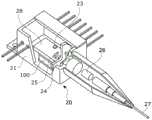
图14是示出蝶型激光二极管(LD)模块的透视图,根据本发明的实施例的热电元件被应用于该蝶型激光二极管(LD)模块。14 is a perspective view illustrating a butterfly laser diode (LD) module to which a thermoelectric element according to an embodiment of the present invention is applied.
蝶型LD模块具有控制温度的功能。Butterfly LD module has the function of controlling temperature.
如图14中所示,蝶型LD模块20包括安设在陶瓷封装21中的热电元件(TEC)100、作为温度传感器的热敏电阻23、LD芯片24和监控光电二极管(MPD)芯片25。As shown in FIG. 14 , the
LD芯片24和MPD芯片25被安设在TEC 100上。陶瓷封装21被气密密封。蝶型LD模块20有利于具有在宽范围中控制带宽和温度的功能。The
使用在陶瓷封装21外侧的透镜26收集光,并且然后将其对准到纤维27。从对准方法的角度来看,蝶型LD模块20也可以称为使用有源对准方法的装置。The light is collected using a
在蝶型LD模块20中,LD芯片24的管芯可以被结合到金属板28的上表面。In the
尽管已经主要参考示例性实施例描述了本发明,但是应该理解,本发明不限于所公开的示例性实施例,并且在不脱离本发明的主旨的情况下,本发明所属领域技术人员能够设计出各种变型和应用。例如,能够修改并且实现在示例性实施例中具体示出的每个构件。应当理解,与这些变型和应用相关的差异将落入由所附权利要求书限定的本发明的范围内。Although the present invention has been mainly described with reference to the exemplary embodiments, it is to be understood that the invention is not limited to the disclosed exemplary embodiments and can be devised by those skilled in the art to which the invention pertains without departing from the gist of the invention. Various variants and applications. For example, each component specifically shown in the exemplary embodiments can be modified and implemented. It should be understood that differences associated with such modifications and applications will fall within the scope of the invention as defined by the appended claims.
附图标记的说明Explanation of reference numerals
120:P型热电支腿 130:N型热电支腿120: P-type thermoelectric leg 130: N-type thermoelectric leg
140:下衬底 150:上衬底140: Lower substrate 150: Upper substrate
161:下电极 162:上电极161: Lower electrode 162: Upper electrode
170、270、370、370:增强件170, 270, 370, 370: Enhancements
Claims (11)
Applications Claiming Priority (3)
| Application Number | Priority Date | Filing Date | Title |
|---|---|---|---|
| KR10-2018-0007116 | 2018-01-19 | ||
| KR1020180007116AKR20190088701A (en) | 2018-01-19 | 2018-01-19 | Thermoelectric element |
| PCT/KR2019/000681WO2019143140A1 (en) | 2018-01-19 | 2019-01-17 | Thermoelectric element |
Publications (2)
| Publication Number | Publication Date |
|---|---|
| CN111615754Atrue CN111615754A (en) | 2020-09-01 |
| CN111615754B CN111615754B (en) | 2024-04-16 |
Family
ID=67302354
Family Applications (1)
| Application Number | Title | Priority Date | Filing Date |
|---|---|---|---|
| CN201980008693.XAActiveCN111615754B (en) | 2018-01-19 | 2019-01-17 | Thermoelectric elements |
Country Status (4)
| Country | Link |
|---|---|
| US (1) | US11508894B2 (en) |
| KR (1) | KR20190088701A (en) |
| CN (1) | CN111615754B (en) |
| WO (1) | WO2019143140A1 (en) |
Cited By (1)
| Publication number | Priority date | Publication date | Assignee | Title |
|---|---|---|---|---|
| CN117766015A (en)* | 2023-11-29 | 2024-03-26 | 北京国家新能源汽车技术创新中心有限公司 | Testing device for double-rate synchronous dynamic random access memory chip |
Families Citing this family (2)
| Publication number | Priority date | Publication date | Assignee | Title |
|---|---|---|---|---|
| KR102693403B1 (en)* | 2019-11-22 | 2024-08-09 | 엘지이노텍 주식회사 | Thermo electric element |
| CN111179778B (en)* | 2020-02-26 | 2022-05-17 | 昆山国显光电有限公司 | Display panel and display device |
Citations (7)
| Publication number | Priority date | Publication date | Assignee | Title |
|---|---|---|---|---|
| JPH08162680A (en)* | 1994-11-30 | 1996-06-21 | Sharp Corp | Thermoelectric converter |
| JP2003318455A (en)* | 2002-04-19 | 2003-11-07 | Da Vinch Co Ltd | Peltier device and manufacturing method thereof |
| CN1937273A (en)* | 2005-08-02 | 2007-03-28 | 株式会社东芝 | Thermoelectric device and manufacturing method thereof |
| JP2009164498A (en)* | 2008-01-10 | 2009-07-23 | Yamaha Corp | Thermoelectric module |
| KR20110036152A (en)* | 2009-10-01 | 2011-04-07 | 엘지이노텍 주식회사 | Photovoltaic device and its manufacturing method |
| CN104810466A (en)* | 2014-01-23 | 2015-07-29 | Lg伊诺特有限公司 | Thermoelectric module and heat conversion device including the same |
| CN106486592A (en)* | 2015-08-28 | 2017-03-08 | 华为技术有限公司 | Electrothermal module and thermoelectricity switch |
Family Cites Families (10)
| Publication number | Priority date | Publication date | Assignee | Title |
|---|---|---|---|---|
| US3615870A (en)* | 1968-09-04 | 1971-10-26 | Rca Corp | Thermoelement array connecting apparatus |
| JP4161572B2 (en)* | 2001-12-27 | 2008-10-08 | ヤマハ株式会社 | Thermoelectric module |
| TWI405361B (en)* | 2008-12-31 | 2013-08-11 | Ind Tech Res Inst | Thermoelectric device and process thereof and stacked structure of chips and chip package structure |
| KR20120028687A (en) | 2010-09-15 | 2012-03-23 | 삼성전기주식회사 | Asymmetry thermoelectric module and manufacturing method thereof |
| JP5638333B2 (en) | 2010-09-30 | 2014-12-10 | 京セラ株式会社 | Thermoelectric module |
| KR20130019883A (en) | 2011-08-18 | 2013-02-27 | 삼성전기주식회사 | Thermoelectric module and manufacturing method for theremoelectric module |
| DE102012102090A1 (en) | 2012-01-31 | 2013-08-01 | Curamik Electronics Gmbh | Thermoelectric generator module, metal-ceramic substrate and method for producing a metal-ceramic substrate |
| KR20160118747A (en) | 2015-04-03 | 2016-10-12 | 엘지이노텍 주식회사 | Thermoelectric device moudule and device using the same |
| JP6794732B2 (en) | 2015-09-28 | 2020-12-02 | 三菱マテリアル株式会社 | Thermoelectric conversion module and thermoelectric conversion device |
| DE112018000874B4 (en)* | 2017-02-15 | 2024-09-12 | Ferrotec Material Technologies Corporation | HOUSING WITH BUILT-IN THERMOELECTRIC ELEMENT |
- 2018
- 2018-01-19KRKR1020180007116Apatent/KR20190088701A/ennot_activeCeased
- 2019
- 2019-01-17USUS16/959,249patent/US11508894B2/enactiveActive
- 2019-01-17WOPCT/KR2019/000681patent/WO2019143140A1/ennot_activeCeased
- 2019-01-17CNCN201980008693.XApatent/CN111615754B/enactiveActive
Patent Citations (7)
| Publication number | Priority date | Publication date | Assignee | Title |
|---|---|---|---|---|
| JPH08162680A (en)* | 1994-11-30 | 1996-06-21 | Sharp Corp | Thermoelectric converter |
| JP2003318455A (en)* | 2002-04-19 | 2003-11-07 | Da Vinch Co Ltd | Peltier device and manufacturing method thereof |
| CN1937273A (en)* | 2005-08-02 | 2007-03-28 | 株式会社东芝 | Thermoelectric device and manufacturing method thereof |
| JP2009164498A (en)* | 2008-01-10 | 2009-07-23 | Yamaha Corp | Thermoelectric module |
| KR20110036152A (en)* | 2009-10-01 | 2011-04-07 | 엘지이노텍 주식회사 | Photovoltaic device and its manufacturing method |
| CN104810466A (en)* | 2014-01-23 | 2015-07-29 | Lg伊诺特有限公司 | Thermoelectric module and heat conversion device including the same |
| CN106486592A (en)* | 2015-08-28 | 2017-03-08 | 华为技术有限公司 | Electrothermal module and thermoelectricity switch |
Cited By (1)
| Publication number | Priority date | Publication date | Assignee | Title |
|---|---|---|---|---|
| CN117766015A (en)* | 2023-11-29 | 2024-03-26 | 北京国家新能源汽车技术创新中心有限公司 | Testing device for double-rate synchronous dynamic random access memory chip |
Also Published As
| Publication number | Publication date |
|---|---|
| KR20190088701A (en) | 2019-07-29 |
| US20200335681A1 (en) | 2020-10-22 |
| CN111615754B (en) | 2024-04-16 |
| US11508894B2 (en) | 2022-11-22 |
| WO2019143140A1 (en) | 2019-07-25 |
Similar Documents
| Publication | Publication Date | Title |
|---|---|---|
| US10903410B2 (en) | Thermoelectric module, and heat conversion apparatus comprising the same | |
| KR102605048B1 (en) | Thermoelectric device moudule | |
| KR102666119B1 (en) | Thermoelectric device moudule and device using the same | |
| US12274171B2 (en) | Thermoelectric element | |
| KR20160117944A (en) | Thermoelectric device moudule and device using the same | |
| CN111615754B (en) | Thermoelectric elements | |
| CN107534077B (en) | Thermoelectric element, thermoelectric module, and heat conversion device including the thermoelectric module | |
| KR20150021366A (en) | Thermoelectric element thermoelectric moudule using the same, and cooling device using thermoelectric moudule | |
| KR102441699B1 (en) | Thermoelectric element | |
| KR102139476B1 (en) | Thermoelectric moudule and device using the same | |
| KR102355281B1 (en) | Thermo electric element | |
| KR102332357B1 (en) | Thermoelectric moudule and device using the same | |
| KR102412389B1 (en) | Thermoelectric device moudule and device using the same | |
| KR20180010060A (en) | Thermo electric element |
Legal Events
| Date | Code | Title | Description |
|---|---|---|---|
| PB01 | Publication | ||
| PB01 | Publication | ||
| SE01 | Entry into force of request for substantive examination | ||
| SE01 | Entry into force of request for substantive examination | ||
| GR01 | Patent grant | ||
| GR01 | Patent grant |