CN111587491A - Semiconductor device and method of manufacturing the same - Google Patents
Semiconductor device and method of manufacturing the sameDownload PDFInfo
- Publication number
- CN111587491A CN111587491ACN201880079059.0ACN201880079059ACN111587491ACN 111587491 ACN111587491 ACN 111587491ACN 201880079059 ACN201880079059 ACN 201880079059ACN 111587491 ACN111587491 ACN 111587491A
- Authority
- CN
- China
- Prior art keywords
- insulator
- oxide
- conductor
- transistor
- film
- Prior art date
- Legal status (The legal status is an assumption and is not a legal conclusion. Google has not performed a legal analysis and makes no representation as to the accuracy of the status listed.)
- Pending
Links
- 239000004065semiconductorSubstances0.000titleclaimsabstractdescription219
- 238000004519manufacturing processMethods0.000titleclaimsdescription31
- 239000012212insulatorSubstances0.000claimsabstractdescription633
- 239000004020conductorSubstances0.000claimsabstractdescription423
- 229910052760oxygenInorganic materials0.000claimsdescription152
- 239000001301oxygenSubstances0.000claimsdescription150
- QVGXLLKOCUKJST-UHFFFAOYSA-Natomic oxygenChemical compound[O]QVGXLLKOCUKJST-UHFFFAOYSA-N0.000claimsdescription146
- 238000000034methodMethods0.000claimsdescription131
- 229910052739hydrogenInorganic materials0.000claimsdescription88
- 239000001257hydrogenSubstances0.000claimsdescription88
- 238000010438heat treatmentMethods0.000claimsdescription82
- UFHFLCQGNIYNRP-UHFFFAOYSA-NHydrogenChemical compound[H][H]UFHFLCQGNIYNRP-UHFFFAOYSA-N0.000claimsdescription80
- 229910044991metal oxideInorganic materials0.000claimsdescription79
- 150000004706metal oxidesChemical class0.000claimsdescription79
- 239000000758substrateSubstances0.000claimsdescription77
- 229910052782aluminiumInorganic materials0.000claimsdescription49
- XAGFODPZIPBFFR-UHFFFAOYSA-NaluminiumChemical compound[Al]XAGFODPZIPBFFR-UHFFFAOYSA-N0.000claimsdescription47
- 238000004544sputter depositionMethods0.000claimsdescription47
- 230000015572biosynthetic processEffects0.000claimsdescription45
- 230000002829reductive effectEffects0.000claimsdescription45
- 229910052735hafniumInorganic materials0.000claimsdescription40
- VBJZVLUMGGDVMO-UHFFFAOYSA-Nhafnium atomChemical compound[Hf]VBJZVLUMGGDVMO-UHFFFAOYSA-N0.000claimsdescription35
- 239000012298atmosphereSubstances0.000claimsdescription15
- PNEYBMLMFCGWSK-UHFFFAOYSA-Naluminium oxideInorganic materials[O-2].[O-2].[O-2].[Al+3].[Al+3]PNEYBMLMFCGWSK-UHFFFAOYSA-N0.000claimsdescription11
- 229910052733galliumInorganic materials0.000claimsdescription11
- 238000012545processingMethods0.000claimsdescription11
- 229910052727yttriumInorganic materials0.000claimsdescription9
- QJGQUHMNIGDVPM-UHFFFAOYSA-Nnitrogen groupChemical group[N]QJGQUHMNIGDVPM-UHFFFAOYSA-N0.000claimsdescription2
- 239000010408filmSubstances0.000description246
- 239000010410layerSubstances0.000description94
- 230000015654memoryEffects0.000description88
- 239000012535impuritySubstances0.000description66
- XUIMIQQOPSSXEZ-UHFFFAOYSA-NSiliconChemical compound[Si]XUIMIQQOPSSXEZ-UHFFFAOYSA-N0.000description55
- 229910052710siliconInorganic materials0.000description55
- 239000010703siliconSubstances0.000description55
- 230000006870functionEffects0.000description53
- VYPSYNLAJGMNEJ-UHFFFAOYSA-NSilicium dioxideChemical compoundO=[Si]=OVYPSYNLAJGMNEJ-UHFFFAOYSA-N0.000description50
- 229910052814silicon oxideInorganic materials0.000description45
- 239000000463materialSubstances0.000description44
- IJGRMHOSHXDMSA-UHFFFAOYSA-NAtomic nitrogenChemical compoundN#NIJGRMHOSHXDMSA-UHFFFAOYSA-N0.000description42
- 239000003990capacitorSubstances0.000description41
- XLYOFNOQVPJJNP-UHFFFAOYSA-NwaterSubstancesOXLYOFNOQVPJJNP-UHFFFAOYSA-N0.000description37
- 229910001868waterInorganic materials0.000description37
- 239000011701zincSubstances0.000description37
- 238000000231atomic layer depositionMethods0.000description36
- 229910052751metalInorganic materials0.000description35
- 238000005229chemical vapour depositionMethods0.000description30
- 238000003860storageMethods0.000description28
- 239000002184metalSubstances0.000description26
- 230000008569processEffects0.000description24
- 229910052721tungstenInorganic materials0.000description23
- 239000010937tungstenSubstances0.000description23
- PXHVJJICTQNCMI-UHFFFAOYSA-NNickelChemical compound[Ni]PXHVJJICTQNCMI-UHFFFAOYSA-N0.000description22
- 238000013473artificial intelligenceMethods0.000description22
- 238000009792diffusion processMethods0.000description22
- WFKWXMTUELFFGS-UHFFFAOYSA-NtungstenChemical compound[W]WFKWXMTUELFFGS-UHFFFAOYSA-N0.000description22
- 125000004429atomChemical group0.000description21
- 229910052757nitrogenInorganic materials0.000description21
- 238000001451molecular beam epitaxyMethods0.000description20
- 238000004549pulsed laser depositionMethods0.000description20
- RYGMFSIKBFXOCR-UHFFFAOYSA-NCopperChemical compound[Cu]RYGMFSIKBFXOCR-UHFFFAOYSA-N0.000description18
- 238000010586diagramMethods0.000description18
- 239000007789gasSubstances0.000description18
- -1hafnium aluminateChemical class0.000description17
- 229910052715tantalumInorganic materials0.000description17
- GUVRBAGPIYLISA-UHFFFAOYSA-Ntantalum atomChemical compound[Ta]GUVRBAGPIYLISA-UHFFFAOYSA-N0.000description17
- RTAQQCXQSZGOHL-UHFFFAOYSA-NTitaniumChemical compound[Ti]RTAQQCXQSZGOHL-UHFFFAOYSA-N0.000description16
- 229910052802copperInorganic materials0.000description16
- 239000010949copperSubstances0.000description16
- 239000013078crystalSubstances0.000description16
- 150000004767nitridesChemical class0.000description16
- TWNQGVIAIRXVLR-UHFFFAOYSA-Noxo(oxoalumanyloxy)alumaneChemical compoundO=[Al]O[Al]=OTWNQGVIAIRXVLR-UHFFFAOYSA-N0.000description16
- 239000010409thin filmSubstances0.000description16
- 229910052719titaniumInorganic materials0.000description16
- 239000010936titaniumSubstances0.000description16
- 229910052581Si3N4Inorganic materials0.000description15
- NRTOMJZYCJJWKI-UHFFFAOYSA-NTitanium nitrideChemical compound[Ti]#NNRTOMJZYCJJWKI-UHFFFAOYSA-N0.000description15
- HQVNEWCFYHHQES-UHFFFAOYSA-Nsilicon nitrideChemical compoundN12[Si]34N5[Si]62N3[Si]51N64HQVNEWCFYHHQES-UHFFFAOYSA-N0.000description15
- 238000005259measurementMethods0.000description14
- 238000001312dry etchingMethods0.000description13
- 230000000694effectsEffects0.000description13
- 229910052707rutheniumInorganic materials0.000description13
- MZLGASXMSKOWSE-UHFFFAOYSA-Ntantalum nitrideChemical compound[Ta]#NMZLGASXMSKOWSE-UHFFFAOYSA-N0.000description13
- OKTJSMMVPCPJKN-UHFFFAOYSA-NCarbonChemical compound[C]OKTJSMMVPCPJKN-UHFFFAOYSA-N0.000description12
- 239000000470constituentSubstances0.000description12
- 230000007547defectEffects0.000description12
- 238000005530etchingMethods0.000description12
- 229910000449hafnium oxideInorganic materials0.000description12
- WIHZLLGSGQNAGK-UHFFFAOYSA-Nhafnium(4+);oxygen(2-)Chemical compound[O-2].[O-2].[Hf+4]WIHZLLGSGQNAGK-UHFFFAOYSA-N0.000description12
- 229910052738indiumInorganic materials0.000description12
- APFVFJFRJDLVQX-UHFFFAOYSA-Nindium atomChemical compound[In]APFVFJFRJDLVQX-UHFFFAOYSA-N0.000description12
- 239000002356single layerSubstances0.000description12
- 230000004888barrier functionEffects0.000description11
- 229910052799carbonInorganic materials0.000description11
- 229910052746lanthanumInorganic materials0.000description11
- FZLIPJUXYLNCLC-UHFFFAOYSA-Nlanthanum atomChemical compound[La]FZLIPJUXYLNCLC-UHFFFAOYSA-N0.000description11
- 229910052759nickelInorganic materials0.000description11
- 239000012299nitrogen atmosphereSubstances0.000description10
- GYHNNYVSQQEPJS-UHFFFAOYSA-NGalliumChemical compound[Ga]GYHNNYVSQQEPJS-UHFFFAOYSA-N0.000description9
- FYYHWMGAXLPEAU-UHFFFAOYSA-NMagnesiumChemical compound[Mg]FYYHWMGAXLPEAU-UHFFFAOYSA-N0.000description9
- ZOKXTWBITQBERF-UHFFFAOYSA-NMolybdenumChemical compound[Mo]ZOKXTWBITQBERF-UHFFFAOYSA-N0.000description9
- KJTLSVCANCCWHF-UHFFFAOYSA-NRutheniumChemical compound[Ru]KJTLSVCANCCWHF-UHFFFAOYSA-N0.000description9
- QCWXUUIWCKQGHC-UHFFFAOYSA-NZirconiumChemical compound[Zr]QCWXUUIWCKQGHC-UHFFFAOYSA-N0.000description9
- 230000008859changeEffects0.000description9
- 239000011229interlayerSubstances0.000description9
- 229910052749magnesiumInorganic materials0.000description9
- 239000011777magnesiumSubstances0.000description9
- 229910052750molybdenumInorganic materials0.000description9
- 239000011733molybdenumSubstances0.000description9
- 230000002093peripheral effectEffects0.000description9
- 229910052726zirconiumInorganic materials0.000description9
- 150000002431hydrogenChemical class0.000description8
- 239000011148porous materialSubstances0.000description8
- 239000011347resinSubstances0.000description8
- 229920005989resinPolymers0.000description8
- XLOMVQKBTHCTTD-UHFFFAOYSA-NZinc monoxideChemical compound[Zn]=OXLOMVQKBTHCTTD-UHFFFAOYSA-N0.000description7
- 229910052796boronInorganic materials0.000description7
- AJNVQOSZGJRYEI-UHFFFAOYSA-Ndigallium;oxygen(2-)Chemical compound[O-2].[O-2].[O-2].[Ga+3].[Ga+3]AJNVQOSZGJRYEI-UHFFFAOYSA-N0.000description7
- 229910001195gallium oxideInorganic materials0.000description7
- 229910052732germaniumInorganic materials0.000description7
- GNPVGFCGXDBREM-UHFFFAOYSA-Ngermanium atomChemical compound[Ge]GNPVGFCGXDBREM-UHFFFAOYSA-N0.000description7
- 125000004430oxygen atomChemical groupO*0.000description7
- 230000035699permeabilityEffects0.000description7
- 229910052712strontiumInorganic materials0.000description7
- VWQVUPCCIRVNHF-UHFFFAOYSA-Nyttrium atomChemical compound[Y]VWQVUPCCIRVNHF-UHFFFAOYSA-N0.000description7
- ZOXJGFHDIHLPTG-UHFFFAOYSA-NBoronChemical compound[B]ZOXJGFHDIHLPTG-UHFFFAOYSA-N0.000description6
- XEEYBQQBJWHFJM-UHFFFAOYSA-NIronChemical compound[Fe]XEEYBQQBJWHFJM-UHFFFAOYSA-N0.000description6
- MWUXSHHQAYIFBG-UHFFFAOYSA-NNitric oxideChemical compoundO=[N]MWUXSHHQAYIFBG-UHFFFAOYSA-N0.000description6
- 239000000956alloySubstances0.000description6
- 238000013461designMethods0.000description6
- 230000005684electric fieldEffects0.000description6
- 230000010354integrationEffects0.000description6
- MRELNEQAGSRDBK-UHFFFAOYSA-Nlanthanum(3+);oxygen(2-)Chemical compound[O-2].[O-2].[O-2].[La+3].[La+3]MRELNEQAGSRDBK-UHFFFAOYSA-N0.000description6
- PLDDOISOJJCEMH-UHFFFAOYSA-Nneodymium(3+);oxygen(2-)Chemical compound[O-2].[O-2].[O-2].[Nd+3].[Nd+3]PLDDOISOJJCEMH-UHFFFAOYSA-N0.000description6
- RVTZCBVAJQQJTK-UHFFFAOYSA-Noxygen(2-);zirconium(4+)Chemical compound[O-2].[O-2].[Zr+4]RVTZCBVAJQQJTK-UHFFFAOYSA-N0.000description6
- 238000009832plasma treatmentMethods0.000description6
- BASFCYQUMIYNBI-UHFFFAOYSA-NplatinumChemical compound[Pt]BASFCYQUMIYNBI-UHFFFAOYSA-N0.000description6
- 229910001925ruthenium oxideInorganic materials0.000description6
- WOCIAKWEIIZHES-UHFFFAOYSA-Nruthenium(iv) oxideChemical compoundO=[Ru]=OWOCIAKWEIIZHES-UHFFFAOYSA-N0.000description6
- CIOAGBVUUVVLOB-UHFFFAOYSA-Nstrontium atomChemical compound[Sr]CIOAGBVUUVVLOB-UHFFFAOYSA-N0.000description6
- 238000002230thermal chemical vapour depositionMethods0.000description6
- 238000001039wet etchingMethods0.000description6
- 229910001928zirconium oxideInorganic materials0.000description6
- PXGOKWXKJXAPGV-UHFFFAOYSA-NFluorineChemical compoundFFPXGOKWXKJXAPGV-UHFFFAOYSA-N0.000description5
- CPLXHLVBOLITMK-UHFFFAOYSA-NMagnesium oxideChemical compound[Mg]=OCPLXHLVBOLITMK-UHFFFAOYSA-N0.000description5
- 229910052779NeodymiumInorganic materials0.000description5
- OAICVXFJPJFONN-UHFFFAOYSA-NPhosphorusChemical compound[P]OAICVXFJPJFONN-UHFFFAOYSA-N0.000description5
- HCHKCACWOHOZIP-UHFFFAOYSA-NZincChemical compound[Zn]HCHKCACWOHOZIP-UHFFFAOYSA-N0.000description5
- 229910052784alkaline earth metalInorganic materials0.000description5
- 238000004140cleaningMethods0.000description5
- 230000007423decreaseEffects0.000description5
- 238000010894electron beam technologyMethods0.000description5
- 238000005516engineering processMethods0.000description5
- 229910052731fluorineInorganic materials0.000description5
- 239000011737fluorineSubstances0.000description5
- 150000002500ionsChemical class0.000description5
- 239000000203mixtureSubstances0.000description5
- 239000002159nanocrystalSubstances0.000description5
- QEFYFXOXNSNQGX-UHFFFAOYSA-Nneodymium atomChemical compound[Nd]QEFYFXOXNSNQGX-UHFFFAOYSA-N0.000description5
- 229910052698phosphorusInorganic materials0.000description5
- 239000011574phosphorusSubstances0.000description5
- 239000000047productSubstances0.000description5
- 238000005406washingMethods0.000description5
- 229910052725zincInorganic materials0.000description5
- XKRFYHLGVUSROY-UHFFFAOYSA-NArgonChemical compound[Ar]XKRFYHLGVUSROY-UHFFFAOYSA-N0.000description4
- ATJFFYVFTNAWJD-UHFFFAOYSA-NTinChemical compound[Sn]ATJFFYVFTNAWJD-UHFFFAOYSA-N0.000description4
- 229910052783alkali metalInorganic materials0.000description4
- 150000001340alkali metalsChemical class0.000description4
- 150000001342alkaline earth metalsChemical class0.000description4
- 229910052790berylliumInorganic materials0.000description4
- ATBAMAFKBVZNFJ-UHFFFAOYSA-Nberyllium atomChemical compound[Be]ATBAMAFKBVZNFJ-UHFFFAOYSA-N0.000description4
- 238000006243chemical reactionMethods0.000description4
- 230000002349favourable effectEffects0.000description4
- YBMRDBCBODYGJE-UHFFFAOYSA-Ngermanium oxideInorganic materialsO=[Ge]=OYBMRDBCBODYGJE-UHFFFAOYSA-N0.000description4
- 239000011810insulating materialSubstances0.000description4
- SIWVEOZUMHYXCS-UHFFFAOYSA-Noxo(oxoyttriooxy)yttriumChemical compoundO=[Y]O[Y]=OSIWVEOZUMHYXCS-UHFFFAOYSA-N0.000description4
- PVADDRMAFCOOPC-UHFFFAOYSA-NoxogermaniumChemical compound[Ge]=OPVADDRMAFCOOPC-UHFFFAOYSA-N0.000description4
- 238000000206photolithographyMethods0.000description4
- 238000001004secondary ion mass spectrometryMethods0.000description4
- 229910052718tinInorganic materials0.000description4
- OGIDPMRJRNCKJF-UHFFFAOYSA-Ntitanium oxideInorganic materials[Ti]=OOGIDPMRJRNCKJF-UHFFFAOYSA-N0.000description4
- 229910052720vanadiumInorganic materials0.000description4
- GPPXJZIENCGNKB-UHFFFAOYSA-NvanadiumChemical compound[V]#[V]GPPXJZIENCGNKB-UHFFFAOYSA-N0.000description4
- 239000011787zinc oxideSubstances0.000description4
- 229910052684CeriumInorganic materials0.000description3
- ZAMOUSCENKQFHK-UHFFFAOYSA-NChlorine atomChemical compound[Cl]ZAMOUSCENKQFHK-UHFFFAOYSA-N0.000description3
- VYZAMTAEIAYCRO-UHFFFAOYSA-NChromiumChemical compound[Cr]VYZAMTAEIAYCRO-UHFFFAOYSA-N0.000description3
- MUBZPKHOEPUJKR-UHFFFAOYSA-NOxalic acidChemical compoundOC(=O)C(O)=OMUBZPKHOEPUJKR-UHFFFAOYSA-N0.000description3
- BQCADISMDOOEFD-UHFFFAOYSA-NSilverChemical compound[Ag]BQCADISMDOOEFD-UHFFFAOYSA-N0.000description3
- 238000003917TEM imageMethods0.000description3
- GWEVSGVZZGPLCZ-UHFFFAOYSA-NTitan oxideChemical compoundO=[Ti]=OGWEVSGVZZGPLCZ-UHFFFAOYSA-N0.000description3
- 238000004833X-ray photoelectron spectroscopyMethods0.000description3
- 229910045601alloyInorganic materials0.000description3
- 238000004458analytical methodMethods0.000description3
- 230000000903blocking effectEffects0.000description3
- 239000000969carrierSubstances0.000description3
- ZMIGMASIKSOYAM-UHFFFAOYSA-NceriumChemical compound[Ce][Ce][Ce][Ce][Ce][Ce][Ce][Ce][Ce][Ce][Ce][Ce][Ce][Ce][Ce][Ce][Ce][Ce][Ce][Ce][Ce][Ce][Ce][Ce][Ce][Ce][Ce][Ce][Ce][Ce][Ce][Ce][Ce][Ce][Ce][Ce][Ce][Ce]ZMIGMASIKSOYAM-UHFFFAOYSA-N0.000description3
- 229910052801chlorineInorganic materials0.000description3
- 239000000460chlorineSubstances0.000description3
- 229910052804chromiumInorganic materials0.000description3
- 239000011651chromiumSubstances0.000description3
- 238000004891communicationMethods0.000description3
- PMHQVHHXPFUNSP-UHFFFAOYSA-Mcopper(1+);methylsulfanylmethane;bromideChemical compoundBr[Cu].CSCPMHQVHHXPFUNSP-UHFFFAOYSA-M0.000description3
- 230000005669field effectEffects0.000description3
- 235000013305foodNutrition0.000description3
- PCHJSUWPFVWCPO-UHFFFAOYSA-NgoldChemical compound[Au]PCHJSUWPFVWCPO-UHFFFAOYSA-N0.000description3
- 229910052737goldInorganic materials0.000description3
- 239000010931goldSubstances0.000description3
- 125000004435hydrogen atomChemical group[H]*0.000description3
- 229910003437indium oxideInorganic materials0.000description3
- PJXISJQVUVHSOJ-UHFFFAOYSA-Nindium(iii) oxideChemical compound[O-2].[O-2].[O-2].[In+3].[In+3]PJXISJQVUVHSOJ-UHFFFAOYSA-N0.000description3
- AMGQUBHHOARCQH-UHFFFAOYSA-Nindium;oxotinChemical compound[In].[Sn]=OAMGQUBHHOARCQH-UHFFFAOYSA-N0.000description3
- 238000009616inductively coupled plasmaMethods0.000description3
- 239000011261inert gasSubstances0.000description3
- 229910052742ironInorganic materials0.000description3
- 239000007788liquidSubstances0.000description3
- 239000000395magnesium oxideSubstances0.000description3
- WPBNNNQJVZRUHP-UHFFFAOYSA-Lmanganese(2+);methyl n-[[2-(methoxycarbonylcarbamothioylamino)phenyl]carbamothioyl]carbamate;n-[2-(sulfidocarbothioylamino)ethyl]carbamodithioateChemical compound[Mn+2].[S-]C(=S)NCCNC([S-])=S.COC(=O)NC(=S)NC1=CC=CC=C1NC(=S)NC(=O)OCWPBNNNQJVZRUHP-UHFFFAOYSA-L0.000description3
- 229910052758niobiumInorganic materials0.000description3
- 239000010955niobiumSubstances0.000description3
- GUCVJGMIXFAOAE-UHFFFAOYSA-Nniobium atomChemical compound[Nb]GUCVJGMIXFAOAE-UHFFFAOYSA-N0.000description3
- QGLKJKCYBOYXKC-UHFFFAOYSA-NnonaoxidotritungstenChemical compoundO=[W]1(=O)O[W](=O)(=O)O[W](=O)(=O)O1QGLKJKCYBOYXKC-UHFFFAOYSA-N0.000description3
- 230000003647oxidationEffects0.000description3
- 238000007254oxidation reactionMethods0.000description3
- 230000001590oxidative effectEffects0.000description3
- BPUBBGLMJRNUCC-UHFFFAOYSA-Noxygen(2-);tantalum(5+)Chemical compound[O-2].[O-2].[O-2].[O-2].[O-2].[Ta+5].[Ta+5]BPUBBGLMJRNUCC-UHFFFAOYSA-N0.000description3
- 230000003071parasitic effectEffects0.000description3
- 229910052697platinumInorganic materials0.000description3
- 229910052709silverInorganic materials0.000description3
- 239000004332silverSubstances0.000description3
- 238000009751slip formingMethods0.000description3
- 239000000126substanceSubstances0.000description3
- 229910001936tantalum oxideInorganic materials0.000description3
- 238000012546transferMethods0.000description3
- 229910001930tungsten oxideInorganic materials0.000description3
- KRHYYFGTRYWZRS-UHFFFAOYSA-NFluoraneChemical compoundFKRHYYFGTRYWZRS-UHFFFAOYSA-N0.000description2
- NBIIXXVUZAFLBC-UHFFFAOYSA-NPhosphoric acidChemical compoundOP(O)(O)=ONBIIXXVUZAFLBC-UHFFFAOYSA-N0.000description2
- MCMNRKCIXSYSNV-UHFFFAOYSA-NZirconium dioxideChemical compoundO=[Zr]=OMCMNRKCIXSYSNV-UHFFFAOYSA-N0.000description2
- 230000002411adverseEffects0.000description2
- 229910052786argonInorganic materials0.000description2
- 238000013528artificial neural networkMethods0.000description2
- 230000006399behaviorEffects0.000description2
- 230000005540biological transmissionEffects0.000description2
- 229910052795boron group elementInorganic materials0.000description2
- 230000006835compressionEffects0.000description2
- 238000007906compressionMethods0.000description2
- 238000013527convolutional neural networkMethods0.000description2
- 238000005520cutting processMethods0.000description2
- 230000003247decreasing effectEffects0.000description2
- 230000002950deficientEffects0.000description2
- 238000003795desorptionMethods0.000description2
- 230000020169heat generationEffects0.000description2
- 230000006872improvementEffects0.000description2
- 238000010884ion-beam techniqueMethods0.000description2
- 229910052741iridiumInorganic materials0.000description2
- GKOZUEZYRPOHIO-UHFFFAOYSA-Niridium atomChemical compound[Ir]GKOZUEZYRPOHIO-UHFFFAOYSA-N0.000description2
- 229910052451lead zirconate titanateInorganic materials0.000description2
- 239000011159matrix materialSubstances0.000description2
- 229910001092metal group alloyInorganic materials0.000description2
- RUFLMLWJRZAWLJ-UHFFFAOYSA-Nnickel silicideChemical compound[Ni]=[Si]=[Ni]RUFLMLWJRZAWLJ-UHFFFAOYSA-N0.000description2
- 229910021334nickel silicideInorganic materials0.000description2
- 125000004433nitrogen atomChemical groupN*0.000description2
- 150000002926oxygenChemical class0.000description2
- 239000012466permeateSubstances0.000description2
- 238000005268plasma chemical vapour depositionMethods0.000description2
- 238000000623plasma-assisted chemical vapour depositionMethods0.000description2
- 229910052696pnictogenInorganic materials0.000description2
- 238000005498polishingMethods0.000description2
- 229910021420polycrystalline siliconInorganic materials0.000description2
- 229920005591polysiliconPolymers0.000description2
- 230000009467reductionEffects0.000description2
- 238000011160researchMethods0.000description2
- 229910021332silicideInorganic materials0.000description2
- 239000000377silicon dioxideSubstances0.000description2
- 239000007787solidSubstances0.000description2
- 239000000243solutionSubstances0.000description2
- 230000007704transitionEffects0.000description2
- YVTHLONGBIQYBO-UHFFFAOYSA-Nzinc indium(3+) oxygen(2-)Chemical compound[O--].[Zn++].[In+3]YVTHLONGBIQYBO-UHFFFAOYSA-N0.000description2
- JBRZTFJDHDCESZ-UHFFFAOYSA-NAsGaChemical compound[As]#[Ga]JBRZTFJDHDCESZ-UHFFFAOYSA-N0.000description1
- UGFAIRIUMAVXCW-UHFFFAOYSA-NCarbon monoxideChemical compound[O+]#[C-]UGFAIRIUMAVXCW-UHFFFAOYSA-N0.000description1
- 229910001218Gallium arsenideInorganic materials0.000description1
- DGAQECJNVWCQMB-PUAWFVPOSA-MIlexoside XXIXChemical compoundC[C@@H]1CC[C@@]2(CC[C@@]3(C(=CC[C@H]4[C@]3(CC[C@@H]5[C@@]4(CC[C@@H](C5(C)C)OS(=O)(=O)[O-])C)C)[C@@H]2[C@]1(C)O)C)C(=O)O[C@H]6[C@@H]([C@H]([C@@H]([C@H](O6)CO)O)O)O.[Na+]DGAQECJNVWCQMB-PUAWFVPOSA-M0.000description1
- GPXJNWSHGFTCBW-UHFFFAOYSA-NIndium phosphideChemical compound[In]#PGPXJNWSHGFTCBW-UHFFFAOYSA-N0.000description1
- WHXSMMKQMYFTQS-UHFFFAOYSA-NLithiumChemical compound[Li]WHXSMMKQMYFTQS-UHFFFAOYSA-N0.000description1
- 239000004677NylonSubstances0.000description1
- 240000007594Oryza sativaSpecies0.000description1
- 235000007164Oryza sativaNutrition0.000description1
- 239000004952PolyamideSubstances0.000description1
- 239000004642PolyimideSubstances0.000description1
- 229910000577Silicon-germaniumInorganic materials0.000description1
- 229910001080W alloyInorganic materials0.000description1
- LEVVHYCKPQWKOP-UHFFFAOYSA-N[Si].[Ge]Chemical compound[Si].[Ge]LEVVHYCKPQWKOP-UHFFFAOYSA-N0.000description1
- 230000001133accelerationEffects0.000description1
- NIXOWILDQLNWCW-UHFFFAOYSA-Nacrylic acid groupChemical groupC(C=C)(=O)ONIXOWILDQLNWCW-UHFFFAOYSA-N0.000description1
- UQZIWOQVLUASCR-UHFFFAOYSA-Nalumane;titaniumChemical compound[AlH3].[Ti]UQZIWOQVLUASCR-UHFFFAOYSA-N0.000description1
- 229910000147aluminium phosphateInorganic materials0.000description1
- 239000007864aqueous solutionSubstances0.000description1
- 239000004760aramidSubstances0.000description1
- 229920003235aromatic polyamidePolymers0.000description1
- 238000004380ashingMethods0.000description1
- 208000003464asthenopiaDiseases0.000description1
- 229910052788bariumInorganic materials0.000description1
- 229910000416bismuth oxideInorganic materials0.000description1
- 229910052800carbon group elementInorganic materials0.000description1
- 230000015556catabolic processEffects0.000description1
- 230000000295complement effectEffects0.000description1
- 150000001875compoundsChemical class0.000description1
- 238000001816coolingMethods0.000description1
- 230000008878couplingEffects0.000description1
- 238000010168coupling processMethods0.000description1
- 238000005859coupling reactionMethods0.000description1
- 238000000151depositionMethods0.000description1
- 230000008021depositionEffects0.000description1
- TYIXMATWDRGMPF-UHFFFAOYSA-Ndibismuth;oxygen(2-)Chemical compound[O-2].[O-2].[O-2].[Bi+3].[Bi+3]TYIXMATWDRGMPF-UHFFFAOYSA-N0.000description1
- 238000007865dilutingMethods0.000description1
- 238000007599dischargingMethods0.000description1
- 238000006073displacement reactionMethods0.000description1
- 230000005611electricityEffects0.000description1
- 238000011156evaluationMethods0.000description1
- 238000000605extractionMethods0.000description1
- 239000000446fuelSubstances0.000description1
- 239000011521glassSubstances0.000description1
- 229910002804graphiteInorganic materials0.000description1
- 239000010439graphiteSubstances0.000description1
- 238000009499grossingMethods0.000description1
- 150000002363hafnium compoundsChemical class0.000description1
- 230000012447hatchingEffects0.000description1
- 238000003384imaging methodMethods0.000description1
- 238000007654immersionMethods0.000description1
- 230000002401inhibitory effectEffects0.000description1
- 238000003475laminationMethods0.000description1
- 238000004093laser heatingMethods0.000description1
- HFGPZNIAWCZYJU-UHFFFAOYSA-Nlead zirconate titanateChemical compound[O-2].[O-2].[O-2].[O-2].[O-2].[Ti+4].[Zr+4].[Pb+2]HFGPZNIAWCZYJU-UHFFFAOYSA-N0.000description1
- 239000004973liquid crystal related substanceSubstances0.000description1
- 229910052744lithiumInorganic materials0.000description1
- AXZKOIWUVFPNLO-UHFFFAOYSA-Nmagnesium;oxygen(2-)Chemical compound[O-2].[Mg+2]AXZKOIWUVFPNLO-UHFFFAOYSA-N0.000description1
- 230000005389magnetismEffects0.000description1
- 230000014759maintenance of locationEffects0.000description1
- 238000002844meltingMethods0.000description1
- 230000008018meltingEffects0.000description1
- 239000007769metal materialSubstances0.000description1
- 238000002488metal-organic chemical vapour depositionMethods0.000description1
- 238000002156mixingMethods0.000description1
- MGRWKWACZDFZJT-UHFFFAOYSA-Nmolybdenum tungstenChemical compound[Mo].[W]MGRWKWACZDFZJT-UHFFFAOYSA-N0.000description1
- 229910000484niobium oxideInorganic materials0.000description1
- URLJKFSTXLNXLG-UHFFFAOYSA-Nniobium(5+);oxygen(2-)Chemical compound[O-2].[O-2].[O-2].[O-2].[O-2].[Nb+5].[Nb+5]URLJKFSTXLNXLG-UHFFFAOYSA-N0.000description1
- 229920001778nylonPolymers0.000description1
- 230000003287optical effectEffects0.000description1
- 230000001151other effectEffects0.000description1
- 235000006408oxalic acidNutrition0.000description1
- 239000002245particleSubstances0.000description1
- 230000000737periodic effectEffects0.000description1
- 230000000704physical effectEffects0.000description1
- 238000001020plasma etchingMethods0.000description1
- 238000007747platingMethods0.000description1
- 229920002647polyamidePolymers0.000description1
- 229920000515polycarbonatePolymers0.000description1
- 239000004417polycarbonateSubstances0.000description1
- 229920000728polyesterPolymers0.000description1
- 229920001721polyimidePolymers0.000description1
- 229920000098polyolefinPolymers0.000description1
- 229920001296polysiloxanePolymers0.000description1
- 239000002243precursorSubstances0.000description1
- 230000001915proofreading effectEffects0.000description1
- 238000011002quantificationMethods0.000description1
- 239000010453quartzSubstances0.000description1
- 230000005855radiationEffects0.000description1
- 238000011084recoveryMethods0.000description1
- 230000000306recurrent effectEffects0.000description1
- 235000009566riceNutrition0.000description1
- 229910052594sapphireInorganic materials0.000description1
- 239000010980sapphireSubstances0.000description1
- HBMJWWWQQXIZIP-UHFFFAOYSA-Nsilicon carbideChemical compound[Si+]#[C-]HBMJWWWQQXIZIP-UHFFFAOYSA-N0.000description1
- 229910010271silicon carbideInorganic materials0.000description1
- 229910052708sodiumInorganic materials0.000description1
- 239000011734sodiumSubstances0.000description1
- 238000004611spectroscopical analysisMethods0.000description1
- 229910002076stabilized zirconiaInorganic materials0.000description1
- VEALVRVVWBQVSL-UHFFFAOYSA-Nstrontium titanateChemical compound[Sr+2].[O-][Ti]([O-])=OVEALVRVVWBQVSL-UHFFFAOYSA-N0.000description1
- 238000006467substitution reactionMethods0.000description1
- 239000013589supplementSubstances0.000description1
- 229910052723transition metalInorganic materials0.000description1
- 150000003624transition metalsChemical class0.000description1
- 230000003936working memoryEffects0.000description1
- 229910001233yttria-stabilized zirconiaInorganic materials0.000description1
Images


Classifications
- C—CHEMISTRY; METALLURGY
- C23—COATING METALLIC MATERIAL; COATING MATERIAL WITH METALLIC MATERIAL; CHEMICAL SURFACE TREATMENT; DIFFUSION TREATMENT OF METALLIC MATERIAL; COATING BY VACUUM EVAPORATION, BY SPUTTERING, BY ION IMPLANTATION OR BY CHEMICAL VAPOUR DEPOSITION, IN GENERAL; INHIBITING CORROSION OF METALLIC MATERIAL OR INCRUSTATION IN GENERAL
- C23C—COATING METALLIC MATERIAL; COATING MATERIAL WITH METALLIC MATERIAL; SURFACE TREATMENT OF METALLIC MATERIAL BY DIFFUSION INTO THE SURFACE, BY CHEMICAL CONVERSION OR SUBSTITUTION; COATING BY VACUUM EVAPORATION, BY SPUTTERING, BY ION IMPLANTATION OR BY CHEMICAL VAPOUR DEPOSITION, IN GENERAL
- C23C14/00—Coating by vacuum evaporation, by sputtering or by ion implantation of the coating forming material
- C23C14/06—Coating by vacuum evaporation, by sputtering or by ion implantation of the coating forming material characterised by the coating material
- C23C14/08—Oxides
- C—CHEMISTRY; METALLURGY
- C23—COATING METALLIC MATERIAL; COATING MATERIAL WITH METALLIC MATERIAL; CHEMICAL SURFACE TREATMENT; DIFFUSION TREATMENT OF METALLIC MATERIAL; COATING BY VACUUM EVAPORATION, BY SPUTTERING, BY ION IMPLANTATION OR BY CHEMICAL VAPOUR DEPOSITION, IN GENERAL; INHIBITING CORROSION OF METALLIC MATERIAL OR INCRUSTATION IN GENERAL
- C23C—COATING METALLIC MATERIAL; COATING MATERIAL WITH METALLIC MATERIAL; SURFACE TREATMENT OF METALLIC MATERIAL BY DIFFUSION INTO THE SURFACE, BY CHEMICAL CONVERSION OR SUBSTITUTION; COATING BY VACUUM EVAPORATION, BY SPUTTERING, BY ION IMPLANTATION OR BY CHEMICAL VAPOUR DEPOSITION, IN GENERAL
- C23C16/00—Chemical coating by decomposition of gaseous compounds, without leaving reaction products of surface material in the coating, i.e. chemical vapour deposition [CVD] processes
- C23C16/22—Chemical coating by decomposition of gaseous compounds, without leaving reaction products of surface material in the coating, i.e. chemical vapour deposition [CVD] processes characterised by the deposition of inorganic material, other than metallic material
- C23C16/30—Deposition of compounds, mixtures or solid solutions, e.g. borides, carbides, nitrides
- C23C16/42—Silicides
- H—ELECTRICITY
- H01—ELECTRIC ELEMENTS
- H01L—SEMICONDUCTOR DEVICES NOT COVERED BY CLASS H10
- H01L21/00—Processes or apparatus adapted for the manufacture or treatment of semiconductor or solid state devices or of parts thereof
- H01L21/02—Manufacture or treatment of semiconductor devices or of parts thereof
- H01L21/02104—Forming layers
- H01L21/02107—Forming insulating materials on a substrate
- H01L21/02109—Forming insulating materials on a substrate characterised by the type of layer, e.g. type of material, porous/non-porous, pre-cursors, mixtures or laminates
- H01L21/02112—Forming insulating materials on a substrate characterised by the type of layer, e.g. type of material, porous/non-porous, pre-cursors, mixtures or laminates characterised by the material of the layer
- H01L21/02172—Forming insulating materials on a substrate characterised by the type of layer, e.g. type of material, porous/non-porous, pre-cursors, mixtures or laminates characterised by the material of the layer the material containing at least one metal element, e.g. metal oxides, metal nitrides, metal oxynitrides or metal carbides
- H01L21/02175—Forming insulating materials on a substrate characterised by the type of layer, e.g. type of material, porous/non-porous, pre-cursors, mixtures or laminates characterised by the material of the layer the material containing at least one metal element, e.g. metal oxides, metal nitrides, metal oxynitrides or metal carbides characterised by the metal
- H01L21/02178—Forming insulating materials on a substrate characterised by the type of layer, e.g. type of material, porous/non-porous, pre-cursors, mixtures or laminates characterised by the material of the layer the material containing at least one metal element, e.g. metal oxides, metal nitrides, metal oxynitrides or metal carbides characterised by the metal the material containing aluminium, e.g. Al2O3
- H—ELECTRICITY
- H01—ELECTRIC ELEMENTS
- H01L—SEMICONDUCTOR DEVICES NOT COVERED BY CLASS H10
- H01L21/00—Processes or apparatus adapted for the manufacture or treatment of semiconductor or solid state devices or of parts thereof
- H01L21/02—Manufacture or treatment of semiconductor devices or of parts thereof
- H01L21/02104—Forming layers
- H01L21/02107—Forming insulating materials on a substrate
- H01L21/02109—Forming insulating materials on a substrate characterised by the type of layer, e.g. type of material, porous/non-porous, pre-cursors, mixtures or laminates
- H01L21/02112—Forming insulating materials on a substrate characterised by the type of layer, e.g. type of material, porous/non-porous, pre-cursors, mixtures or laminates characterised by the material of the layer
- H01L21/02172—Forming insulating materials on a substrate characterised by the type of layer, e.g. type of material, porous/non-porous, pre-cursors, mixtures or laminates characterised by the material of the layer the material containing at least one metal element, e.g. metal oxides, metal nitrides, metal oxynitrides or metal carbides
- H01L21/02175—Forming insulating materials on a substrate characterised by the type of layer, e.g. type of material, porous/non-porous, pre-cursors, mixtures or laminates characterised by the material of the layer the material containing at least one metal element, e.g. metal oxides, metal nitrides, metal oxynitrides or metal carbides characterised by the metal
- H01L21/02181—Forming insulating materials on a substrate characterised by the type of layer, e.g. type of material, porous/non-porous, pre-cursors, mixtures or laminates characterised by the material of the layer the material containing at least one metal element, e.g. metal oxides, metal nitrides, metal oxynitrides or metal carbides characterised by the metal the material containing hafnium, e.g. HfO2
- H—ELECTRICITY
- H01—ELECTRIC ELEMENTS
- H01L—SEMICONDUCTOR DEVICES NOT COVERED BY CLASS H10
- H01L21/00—Processes or apparatus adapted for the manufacture or treatment of semiconductor or solid state devices or of parts thereof
- H01L21/02—Manufacture or treatment of semiconductor devices or of parts thereof
- H01L21/02104—Forming layers
- H01L21/02107—Forming insulating materials on a substrate
- H01L21/02225—Forming insulating materials on a substrate characterised by the process for the formation of the insulating layer
- H01L21/0226—Forming insulating materials on a substrate characterised by the process for the formation of the insulating layer formation by a deposition process
- H01L21/02263—Forming insulating materials on a substrate characterised by the process for the formation of the insulating layer formation by a deposition process deposition from the gas or vapour phase
- H01L21/02266—Forming insulating materials on a substrate characterised by the process for the formation of the insulating layer formation by a deposition process deposition from the gas or vapour phase deposition by physical ablation of a target, e.g. sputtering, reactive sputtering, physical vapour deposition or pulsed laser deposition
- H—ELECTRICITY
- H01—ELECTRIC ELEMENTS
- H01L—SEMICONDUCTOR DEVICES NOT COVERED BY CLASS H10
- H01L21/00—Processes or apparatus adapted for the manufacture or treatment of semiconductor or solid state devices or of parts thereof
- H01L21/02—Manufacture or treatment of semiconductor devices or of parts thereof
- H01L21/02104—Forming layers
- H01L21/02365—Forming inorganic semiconducting materials on a substrate
- H01L21/02518—Deposited layers
- H01L21/02521—Materials
- H01L21/02565—Oxide semiconducting materials not being Group 12/16 materials, e.g. ternary compounds
- H—ELECTRICITY
- H01—ELECTRIC ELEMENTS
- H01L—SEMICONDUCTOR DEVICES NOT COVERED BY CLASS H10
- H01L21/00—Processes or apparatus adapted for the manufacture or treatment of semiconductor or solid state devices or of parts thereof
- H01L21/02—Manufacture or treatment of semiconductor devices or of parts thereof
- H01L21/02104—Forming layers
- H01L21/02365—Forming inorganic semiconducting materials on a substrate
- H01L21/02612—Formation types
- H01L21/02617—Deposition types
- H01L21/02631—Physical deposition at reduced pressure, e.g. MBE, sputtering, evaporation
- H—ELECTRICITY
- H01—ELECTRIC ELEMENTS
- H01L—SEMICONDUCTOR DEVICES NOT COVERED BY CLASS H10
- H01L21/00—Processes or apparatus adapted for the manufacture or treatment of semiconductor or solid state devices or of parts thereof
- H01L21/02—Manufacture or treatment of semiconductor devices or of parts thereof
- H01L21/04—Manufacture or treatment of semiconductor devices or of parts thereof the devices having potential barriers, e.g. a PN junction, depletion layer or carrier concentration layer
- H01L21/18—Manufacture or treatment of semiconductor devices or of parts thereof the devices having potential barriers, e.g. a PN junction, depletion layer or carrier concentration layer the devices having semiconductor bodies comprising elements of Group IV of the Periodic Table or AIIIBV compounds with or without impurities, e.g. doping materials
- H01L21/28—Manufacture of electrodes on semiconductor bodies using processes or apparatus not provided for in groups H01L21/20 - H01L21/268
- H—ELECTRICITY
- H01—ELECTRIC ELEMENTS
- H01L—SEMICONDUCTOR DEVICES NOT COVERED BY CLASS H10
- H01L21/00—Processes or apparatus adapted for the manufacture or treatment of semiconductor or solid state devices or of parts thereof
- H01L21/02—Manufacture or treatment of semiconductor devices or of parts thereof
- H01L21/04—Manufacture or treatment of semiconductor devices or of parts thereof the devices having potential barriers, e.g. a PN junction, depletion layer or carrier concentration layer
- H01L21/34—Manufacture or treatment of semiconductor devices or of parts thereof the devices having potential barriers, e.g. a PN junction, depletion layer or carrier concentration layer the devices having semiconductor bodies not provided for in groups H01L21/18, H10D48/04 and H10D48/07, with or without impurities, e.g. doping materials
- H01L21/46—Treatment of semiconductor bodies using processes or apparatus not provided for in groups H01L21/428
- H01L21/477—Thermal treatment for modifying the properties of semiconductor bodies, e.g. annealing, sintering
- H—ELECTRICITY
- H10—SEMICONDUCTOR DEVICES; ELECTRIC SOLID-STATE DEVICES NOT OTHERWISE PROVIDED FOR
- H10B—ELECTRONIC MEMORY DEVICES
- H10B12/00—Dynamic random access memory [DRAM] devices
- H—ELECTRICITY
- H10—SEMICONDUCTOR DEVICES; ELECTRIC SOLID-STATE DEVICES NOT OTHERWISE PROVIDED FOR
- H10D—INORGANIC ELECTRIC SEMICONDUCTOR DEVICES
- H10D30/00—Field-effect transistors [FET]
- H10D30/60—Insulated-gate field-effect transistors [IGFET]
- H10D30/67—Thin-film transistors [TFT]
- H10D30/6704—Thin-film transistors [TFT] having supplementary regions or layers in the thin films or in the insulated bulk substrates for controlling properties of the device
- H—ELECTRICITY
- H10—SEMICONDUCTOR DEVICES; ELECTRIC SOLID-STATE DEVICES NOT OTHERWISE PROVIDED FOR
- H10D—INORGANIC ELECTRIC SEMICONDUCTOR DEVICES
- H10D30/00—Field-effect transistors [FET]
- H10D30/60—Insulated-gate field-effect transistors [IGFET]
- H10D30/67—Thin-film transistors [TFT]
- H10D30/6729—Thin-film transistors [TFT] characterised by the electrodes
- H10D30/673—Thin-film transistors [TFT] characterised by the electrodes characterised by the shapes, relative sizes or dispositions of the gate electrodes
- H10D30/6733—Multi-gate TFTs
- H10D30/6734—Multi-gate TFTs having gate electrodes arranged on both top and bottom sides of the channel, e.g. dual-gate TFTs
- H—ELECTRICITY
- H10—SEMICONDUCTOR DEVICES; ELECTRIC SOLID-STATE DEVICES NOT OTHERWISE PROVIDED FOR
- H10D—INORGANIC ELECTRIC SEMICONDUCTOR DEVICES
- H10D30/00—Field-effect transistors [FET]
- H10D30/60—Insulated-gate field-effect transistors [IGFET]
- H10D30/67—Thin-film transistors [TFT]
- H10D30/674—Thin-film transistors [TFT] characterised by the active materials
- H10D30/6755—Oxide semiconductors, e.g. zinc oxide, copper aluminium oxide or cadmium stannate
- H—ELECTRICITY
- H10—SEMICONDUCTOR DEVICES; ELECTRIC SOLID-STATE DEVICES NOT OTHERWISE PROVIDED FOR
- H10D—INORGANIC ELECTRIC SEMICONDUCTOR DEVICES
- H10D30/00—Field-effect transistors [FET]
- H10D30/60—Insulated-gate field-effect transistors [IGFET]
- H10D30/67—Thin-film transistors [TFT]
- H10D30/6757—Thin-film transistors [TFT] characterised by the structure of the channel, e.g. transverse or longitudinal shape or doping profile
- H—ELECTRICITY
- H10—SEMICONDUCTOR DEVICES; ELECTRIC SOLID-STATE DEVICES NOT OTHERWISE PROVIDED FOR
- H10D—INORGANIC ELECTRIC SEMICONDUCTOR DEVICES
- H10D62/00—Semiconductor bodies, or regions thereof, of devices having potential barriers
- H10D62/80—Semiconductor bodies, or regions thereof, of devices having potential barriers characterised by the materials
- H—ELECTRICITY
- H10—SEMICONDUCTOR DEVICES; ELECTRIC SOLID-STATE DEVICES NOT OTHERWISE PROVIDED FOR
- H10D—INORGANIC ELECTRIC SEMICONDUCTOR DEVICES
- H10D86/00—Integrated devices formed in or on insulating or conducting substrates, e.g. formed in silicon-on-insulator [SOI] substrates or on stainless steel or glass substrates
- H10D86/40—Integrated devices formed in or on insulating or conducting substrates, e.g. formed in silicon-on-insulator [SOI] substrates or on stainless steel or glass substrates characterised by multiple TFTs
- H10D86/421—Integrated devices formed in or on insulating or conducting substrates, e.g. formed in silicon-on-insulator [SOI] substrates or on stainless steel or glass substrates characterised by multiple TFTs having a particular composition, shape or crystalline structure of the active layer
- H10D86/423—Integrated devices formed in or on insulating or conducting substrates, e.g. formed in silicon-on-insulator [SOI] substrates or on stainless steel or glass substrates characterised by multiple TFTs having a particular composition, shape or crystalline structure of the active layer comprising semiconductor materials not belonging to the Group IV, e.g. InGaZnO
- H—ELECTRICITY
- H10—SEMICONDUCTOR DEVICES; ELECTRIC SOLID-STATE DEVICES NOT OTHERWISE PROVIDED FOR
- H10D—INORGANIC ELECTRIC SEMICONDUCTOR DEVICES
- H10D86/00—Integrated devices formed in or on insulating or conducting substrates, e.g. formed in silicon-on-insulator [SOI] substrates or on stainless steel or glass substrates
- H10D86/40—Integrated devices formed in or on insulating or conducting substrates, e.g. formed in silicon-on-insulator [SOI] substrates or on stainless steel or glass substrates characterised by multiple TFTs
- H10D86/441—Interconnections, e.g. scanning lines
- H—ELECTRICITY
- H10—SEMICONDUCTOR DEVICES; ELECTRIC SOLID-STATE DEVICES NOT OTHERWISE PROVIDED FOR
- H10D—INORGANIC ELECTRIC SEMICONDUCTOR DEVICES
- H10D86/00—Integrated devices formed in or on insulating or conducting substrates, e.g. formed in silicon-on-insulator [SOI] substrates or on stainless steel or glass substrates
- H10D86/40—Integrated devices formed in or on insulating or conducting substrates, e.g. formed in silicon-on-insulator [SOI] substrates or on stainless steel or glass substrates characterised by multiple TFTs
- H10D86/481—Integrated devices formed in or on insulating or conducting substrates, e.g. formed in silicon-on-insulator [SOI] substrates or on stainless steel or glass substrates characterised by multiple TFTs integrated with passive devices, e.g. auxiliary capacitors
- H—ELECTRICITY
- H10—SEMICONDUCTOR DEVICES; ELECTRIC SOLID-STATE DEVICES NOT OTHERWISE PROVIDED FOR
- H10D—INORGANIC ELECTRIC SEMICONDUCTOR DEVICES
- H10D86/00—Integrated devices formed in or on insulating or conducting substrates, e.g. formed in silicon-on-insulator [SOI] substrates or on stainless steel or glass substrates
- H10D86/40—Integrated devices formed in or on insulating or conducting substrates, e.g. formed in silicon-on-insulator [SOI] substrates or on stainless steel or glass substrates characterised by multiple TFTs
- H10D86/60—Integrated devices formed in or on insulating or conducting substrates, e.g. formed in silicon-on-insulator [SOI] substrates or on stainless steel or glass substrates characterised by multiple TFTs wherein the TFTs are in active matrices
- H—ELECTRICITY
- H10—SEMICONDUCTOR DEVICES; ELECTRIC SOLID-STATE DEVICES NOT OTHERWISE PROVIDED FOR
- H10D—INORGANIC ELECTRIC SEMICONDUCTOR DEVICES
- H10D87/00—Integrated devices comprising both bulk components and either SOI or SOS components on the same substrate
- H—ELECTRICITY
- H10—SEMICONDUCTOR DEVICES; ELECTRIC SOLID-STATE DEVICES NOT OTHERWISE PROVIDED FOR
- H10D—INORGANIC ELECTRIC SEMICONDUCTOR DEVICES
- H10D99/00—Subject matter not provided for in other groups of this subclass
Landscapes
- Engineering & Computer Science (AREA)
- Physics & Mathematics (AREA)
- Condensed Matter Physics & Semiconductors (AREA)
- General Physics & Mathematics (AREA)
- Manufacturing & Machinery (AREA)
- Computer Hardware Design (AREA)
- Microelectronics & Electronic Packaging (AREA)
- Power Engineering (AREA)
- Chemical & Material Sciences (AREA)
- Materials Engineering (AREA)
- Chemical Kinetics & Catalysis (AREA)
- Mechanical Engineering (AREA)
- Metallurgy (AREA)
- Organic Chemistry (AREA)
- Optics & Photonics (AREA)
- Inorganic Chemistry (AREA)
- General Chemical & Material Sciences (AREA)
- Thin Film Transistor (AREA)
- Electrodes Of Semiconductors (AREA)
- Metal-Oxide And Bipolar Metal-Oxide Semiconductor Integrated Circuits (AREA)
- Semiconductor Memories (AREA)
- Physical Vapour Deposition (AREA)
Abstract
Description
Translated fromChinese技术领域technical field
本发明的一个方式涉及一种半导体装置及半导体装置的制造方法。此外,本发明的一个方式涉及一种半导体晶片、模块以及电子设备。One embodiment of the present invention relates to a semiconductor device and a method of manufacturing the semiconductor device. Furthermore, one aspect of the present invention relates to a semiconductor wafer, a module, and an electronic device.
注意,在本说明书等中,半导体装置是指能够通过利用半导体特性而工作的所有装置。除了晶体管等的半导体元件之外,半导体电路、运算装置或存储装置也是半导体装置的一个方式。显示装置(液晶显示装置、发光显示装置等)、投影装置、照明装置、电光装置、蓄电装置、存储装置、半导体电路、成像装置及电子设备等有时包括半导体装置。Note that, in this specification and the like, a semiconductor device refers to all devices that can operate by utilizing semiconductor characteristics. In addition to semiconductor elements such as transistors, a semiconductor circuit, an arithmetic device, or a storage device is also one form of a semiconductor device. Display devices (liquid crystal display devices, light-emitting display devices, etc.), projection devices, lighting devices, electro-optical devices, power storage devices, storage devices, semiconductor circuits, imaging devices, electronic equipment, and the like may include semiconductor devices.
注意,本发明的一个方式不局限于上述技术领域。本说明书等所公开的发明的一个方式涉及一种物体、方法或制造方法。另外,本发明的一个方式涉及一种工序(process)、机器(machine)、产品(manufacture)或者组合物(composition of matter)。Note that one form of the present invention is not limited to the above-mentioned technical field. One aspect of the invention disclosed in this specification and the like relates to an object, a method, or a manufacturing method. Moreover, one form of this invention relates to a process (process), machine (machine), product (manufacture) or composition (composition of matter).
背景技术Background technique
作为可以应用于晶体管的半导体薄膜,硅类半导体材料被广泛地周知。另外,作为其他材料,氧化物半导体受到关注。作为氧化物半导体,例如,已知除了如氧化铟、氧化锌等单元金属氧化物之外还有多元金属氧化物。在多元金属氧化物中,有关In-Ga-Zn氧化物(以下也称为IGZO)的研究尤为火热。Silicon-based semiconductor materials are widely known as semiconductor thin films that can be applied to transistors. In addition, as other materials, oxide semiconductors are attracting attention. As the oxide semiconductor, for example, multi-component metal oxides are known in addition to unitary metal oxides such as indium oxide and zinc oxide. Among the multi-component metal oxides, the research on In-Ga-Zn oxide (hereinafter also referred to as IGZO) is particularly hot.
通过对IGZO的研究,在氧化物半导体中,发现了既不是单晶也不是非晶的CAAC(c-axis aligned crystalline)结构及nc(nanocrystalline)结构(参照非专利文献1至非专利文献3)。非专利文献1及非专利文献2中公开了一种使用具有CAAC结构的氧化物半导体制造晶体管的技术。再者,非专利文献4及非专利文献5中公开了一种比CAAC结构及nc结构的结晶性更低的氧化物半导体中也具有微小的结晶。Through research on IGZO, the oxide semiconductors have found a CAAC (c-axis aligned crystalline) structure and an nc (nanocrystalline) structure that are neither single crystal nor amorphous (refer to Non-Patent
将IGZO用于活性层的晶体管具有极低的关态电流(参照非专利文献6),已知有利用了该特性的LSI及显示器(参照非专利文献7及非专利文献8)。A transistor using IGZO as an active layer has an extremely low off-state current (see Non-Patent Document 6), and LSIs and displays utilizing this characteristic are known (see Non-Patent Document 7 and Non-Patent Document 8).
[先行技术文献][Prior Technology Literature]
[非专利文献][Non-patent literature]
[非专利文献1]S.Yamazaki et al.,“SID Symposium Digest of TechnicalPapers”,2012,volume 43,issue 1,p.183-186[Non-Patent Document 1] S. Yamazaki et al., "SID Symposium Digest of Technical Papers", 2012, volume 43,
[非专利文献2]S.Yamazaki et al.,“Japanese Journal of Applied Physics”,2014,volume 53,Number 4S,p.04ED18-1-04ED18-10[Non-Patent Document 2] S. Yamazaki et al., "Japanese Journal of Applied Physics", 2014, volume 53, Number 4S, p.04ED18-1-04ED18-10
[非专利文献3]S.Ito et al.,“The Proceedings of AM-FPD’13Digest ofTechnical Papers”,2013,p.151-154[Non-Patent Document 3] S.Ito et al., "The Proceedings of AM-FPD' 13 Digest of Technical Papers", 2013, p.151-154
[非专利文献4]S.Yamazaki et al.,“ECS Journal of Solid State Science andTechnology”,2014,volume 3,issue 9,p.Q3012-Q3022[Non-Patent Document 4] S. Yamazaki et al., "ECS Journal of Solid State Science and Technology", 2014,
[非专利文献5]S.Yamazaki,“ECS Transactions”,2014,volume 64,issue 10,p.155-164[Non-Patent Document 5] S. Yamazaki, "ECS Transactions", 2014, volume 64,
[非专利文献6]K.Kato et al.,“Japanese Journal of Applied Physics”,2012,volume 51,p.021201-1-021201-7[Non-Patent Document 6] K. Kato et al., "Japanese Journal of Applied Physics", 2012, volume 51, p.021201-1-021201-7
[非专利文献7]S.Matsuda et al.,“2015Symposium on VLSI Technology Digest ofTechnical Papers”,2015,p.T216-T217[Non-Patent Document 7] S. Matsuda et al., "2015 Symposium on VLSI Technology Digest of Technical Papers", 2015, p.T216-T217
[非专利文献8]S.Amano et al.,“SID Symposium Digest of Technical Papers”,2010,volume 41,issue 1,p.626-629[Non-Patent Document 8] S. Amano et al., "SID Symposium Digest of Technical Papers", 2010, volume 41,
发明内容SUMMARY OF THE INVENTION
发明所要解决的技术问题The technical problem to be solved by the invention
本发明的一个方式的目的之一是提供一种通态电流大的半导体装置。另外,本发明的一个方式的目的之一是提供一种具有高频率特性的半导体装置。另外,本发明的一个方式的目的之一是提供一种可靠性良好的半导体装置。另外,本发明的一个方式的目的之一是提供一种能够进行微型化或高集成化的半导体装置。另外,本发明的一个方式的目的之一是提供一种具有良好的电特性的半导体装置。另外,本发明的一个方式的目的之一是提供一种生産率高的半导体装置。An object of one embodiment of the present invention is to provide a semiconductor device with a large on-state current. Another object of one embodiment of the present invention is to provide a semiconductor device having high frequency characteristics. Another object of one embodiment of the present invention is to provide a highly reliable semiconductor device. Another object of one embodiment of the present invention is to provide a semiconductor device capable of miniaturization or high integration. Another object of one embodiment of the present invention is to provide a semiconductor device having favorable electrical characteristics. Another object of one aspect of the present invention is to provide a semiconductor device with high productivity.
本发明的一个方式的目的之一是提供一种能够长期间保持数据的半导体装置。本发明的一个方式的目的之一是提供一种数据的写入速度快的半导体装置。本发明的一个方式的目的之一是提供一种设计自由度高的半导体装置。本发明的一个方式的目的之一是提供一种能够抑制功耗的半导体装置。本发明的一个方式的目的之一是提供一种新颖的半导体装置。One of the objects of one embodiment of the present invention is to provide a semiconductor device capable of holding data for a long period of time. One of the objects of one embodiment of the present invention is to provide a semiconductor device with a high data writing speed. One of the objects of one embodiment of the present invention is to provide a semiconductor device with a high degree of design freedom. An object of one embodiment of the present invention is to provide a semiconductor device capable of suppressing power consumption. One of the objects of one embodiment of the present invention is to provide a novel semiconductor device.
注意,上述目的的记载不妨碍其他目的的存在。此外,本发明的一个方式并不需要实现所有上述目的。另外,这些目的之外的目的根据说明书、附图、权利要求书等的记载来看是自然明了的,可以从说明书、附图、权利要求书等的记载得出上述以外的目的。Note that the description of the above purpose does not prevent the existence of other purposes. Furthermore, one form of the present invention need not achieve all of the above-mentioned objects. In addition, objects other than the above-mentioned objects are obvious from the description of the specification, drawings, claims, and the like, and objects other than the above-mentioned objects can be derived from the description of the specification, drawings, claims, and the like.
解决技术问题的手段means of solving technical problems
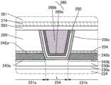
本发明的一个方式是一种半导体装置,包括:第一绝缘体;第一绝缘体上的第一氧化物;第一氧化物上的第二氧化物;第二氧化物上的第一导电体及第二导电体;第二氧化物上的第三氧化物;第三氧化物上的第二绝缘体;位于第二绝缘体上并与第三氧化物重叠的第三导电体;与第一绝缘体上、第一氧化物的侧面、第二氧化物的侧面、第一导电体的侧面、第一导电体的顶面、第二导电体的侧面、第二导电体的顶面接触的第三绝缘体;以及第三导电体、第二绝缘体、第三氧化物及第三绝缘体上的第四绝缘体,其中,第四绝缘体与第三导电体、第二绝缘体及第三氧化物的每一个的顶面接触。One aspect of the present invention is a semiconductor device including: a first insulator; a first oxide on the first insulator; a second oxide on the first oxide; a first conductor and a second oxide on the second oxide Second conductor; third oxide on second oxide; second insulator on third oxide; third conductor on second insulator and overlapping third oxide; The side of the monoxide, the side of the second oxide, the side of the first electrical conductor, the top of the first electrical conductor, the side of the second electrical conductor, the third insulator with which the top of the second electrical conductor is in contact; and Three conductors, a second insulator, a third oxide, and a fourth insulator on the third insulator, wherein the fourth insulator is in contact with a top surface of each of the third conductor, the second insulator, and the third oxide.
此外,第三绝缘体和第四绝缘体优选都比第一绝缘体难以使氧及氢中的一方或双方透过。In addition, it is preferable that both the third insulator and the fourth insulator are more difficult to transmit one or both of oxygen and hydrogen than the first insulator.
此外,第三绝缘体和第四绝缘体优选都比第二绝缘体难以使氧及氢中的一方或双方透过。In addition, it is preferable that both the third insulator and the fourth insulator are less likely to transmit one or both of oxygen and hydrogen than the second insulator.
此外,第三绝缘体和第四绝缘体优选都是包含铝及铪中的一方或双方的氧化物。In addition, it is preferable that both the third insulator and the fourth insulator contain oxides of one or both of aluminum and hafnium.
此外,第三绝缘体和第四绝缘体优选都是氧化铝。Furthermore, the third insulator and the fourth insulator are preferably both alumina.
此外,第一至第三氧化物优选具有In、元素M(M是Al、Ga、Y或Sn)及Zn。Further, the first to third oxides preferably have In, elements M (M is Al, Ga, Y, or Sn), and Zn.
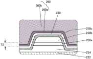
此外,本发明的一个方式是一种包括晶体管的半导体装置,其中,晶体管包括:第一绝缘体;第一绝缘体上的第一氧化物;第一氧化物上的第二氧化物;第二氧化物上的第一导电体及第二导电体;第二氧化物上的第三氧化物;第三氧化物上的第二绝缘体;以及位于第二绝缘体上并与第三氧化物重叠的第三导电体,在晶体管的沟道长度方向上的截面中,以第一绝缘体的底面的高度为标准,与第二氧化物重叠的区域中的第三导电体的底面的高度比第二导电体的顶面的高度低,并且,在晶体管的沟道宽度方向上的截面中,以第一绝缘体的底面的高度为标准,不与第二氧化物重叠的区域中的第三导电体的底面的高度比第二氧化物的底面的高度低。Furthermore, one aspect of the present invention is a semiconductor device including a transistor, wherein the transistor includes: a first insulator; a first oxide on the first insulator; a second oxide on the first oxide; a second oxide a first conductor and a second conductor on the second oxide; a third oxide on the second oxide; a second insulator on the third oxide; and a third conductor on the second insulator and overlapping the third oxide In the cross section in the channel length direction of the transistor, the height of the bottom surface of the first insulator is used as the standard, and the height of the bottom surface of the third conductor in the region overlapping with the second oxide is higher than the height of the top surface of the second conductor. The height of the surface is low, and the height of the bottom surface of the third conductor in the region that does not overlap with the second oxide is higher than the height of the bottom surface of the first insulator in the cross section in the channel width direction of the transistor. The height of the bottom surface of the second oxide is low.
此外,本发明的一个方式是一种半导体装置的制造方法,包括如下步骤:在衬底上形成第一绝缘体;在第一绝缘体上依次形成第一氧化膜及第一导电膜;对第一氧化膜及第一导电膜进行加工来形成第一氧化物及导电体层;以覆盖第一氧化物及导电体层的方式依次形成第一绝缘膜及第二绝缘膜;通过在导电体层、第一绝缘膜及第二绝缘膜中形成使第一氧化物露出的开口,形成第一导电体、第二导电体及第二绝缘体;进行第一加热处理形成第二氧化膜;进行第二加热处理形成第三绝缘膜;形成第二导电膜;通过进行平坦化处理,直到第二绝缘膜的一部分露出为止去除第二氧化膜、第三绝缘膜及第二导电膜,来形成第二氧化物、第三绝缘体及第三导电体;以覆盖第二绝缘膜、第二氧化物、第三绝缘体及第三导电体的方式形成第四绝缘膜;以及进行第三加热处理。In addition, one aspect of the present invention is a method of manufacturing a semiconductor device, comprising the steps of: forming a first insulator on a substrate; sequentially forming a first oxide film and a first conductive film on the first insulator; The film and the first conductive film are processed to form the first oxide and the conductor layer; the first insulating film and the second insulating film are sequentially formed so as to cover the first oxide and the conductor layer; An opening that exposes the first oxide is formed in an insulating film and a second insulating film to form a first conductor, a second conductor and a second insulator; a first heat treatment is performed to form a second oxide film; a second heat treatment is performed forming a third insulating film; forming a second conductive film; and removing the second oxide film, the third insulating film, and the second conductive film by performing a planarization process until a part of the second insulating film is exposed to form a second oxide, a third insulator and a third conductor; a fourth insulating film is formed so as to cover the second insulating film, the second oxide, the third insulator and the third conductor; and a third heat treatment is performed.
此外,优选在减压下依次进行第一加热处理及第二氧化膜的成膜。In addition, it is preferable to perform the first heat treatment and the film formation of the second oxide film in this order under reduced pressure.
此外,优选在减压下依次进行第二加热处理及第三绝缘膜的成膜。In addition, it is preferable to perform the second heat treatment and the film formation of the third insulating film in this order under reduced pressure.
此外,优选在含氮的气氛下进行第三加热处理。Further, it is preferable to perform the third heat treatment in a nitrogen-containing atmosphere.
此外,优选作为第四绝缘膜,通过采用溅射法形成包含铝的金属氧化物。Further, as the fourth insulating film, it is preferable to form a metal oxide containing aluminum by using a sputtering method.
发明效果Invention effect
通过本发明的一个方式,可以提供一种通态电流大的半导体装置。另外,通过本发明的一个方式,可以提供一种具有高频率特性的半导体装置。另外,通过本发明的一个方式,可以提供一种可靠性良好的半导体装置。另外,通过本发明的一个方式,可以提供一种能够实现微型化或高集成化的半导体装置。另外,通过本发明的一个方式,可以提供一种具有良好的电特性的半导体装置。另外,通过本发明的一个方式,可以提供一种生产率高的半导体装置。According to one aspect of the present invention, a semiconductor device having a large on-state current can be provided. In addition, according to one aspect of the present invention, a semiconductor device having high frequency characteristics can be provided. In addition, according to one aspect of the present invention, a semiconductor device with high reliability can be provided. In addition, according to one aspect of the present invention, a semiconductor device capable of miniaturization or high integration can be provided. In addition, according to one aspect of the present invention, a semiconductor device having favorable electrical characteristics can be provided. In addition, according to one aspect of the present invention, a semiconductor device with high productivity can be provided.
另外,可以提供一种能够长期间保持数据的半导体装置。另外,可以提供一种数据的写入速度快的半导体装置。另外,可以提供一种设计自由度高的半导体装置。另外,可以提供一种能够抑制功耗的半导体装置。另外,可以提供一种新颖的半导体装置。In addition, a semiconductor device capable of holding data for a long period of time can be provided. In addition, a semiconductor device with a high data writing speed can be provided. In addition, a semiconductor device with a high degree of design freedom can be provided. In addition, a semiconductor device capable of suppressing power consumption can be provided. In addition, a novel semiconductor device can be provided.
注意,这些效果的记载不妨碍其他效果的存在。此外,本发明的一个方式并不需要具有所有上述效果。另外,这些效果之外的效果根据说明书、附图、权利要求书等的记载来看是自然明了的,可以从说明书、附图、权利要求书等的记载得出上述以外的效果。Note that the description of these effects does not prevent the existence of other effects. Furthermore, one embodiment of the present invention does not need to have all of the above-described effects. In addition, effects other than these effects are obvious from the description of the specification, drawings, claims, and the like, and effects other than the above can be obtained from the description of the specification, drawings, claims, and the like.
附图简要说明Brief Description of Drawings
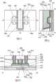
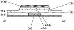
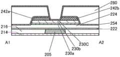
[图1]根据本发明的一个方式的半导体装置的俯视图及截面图。1 is a plan view and a cross-sectional view of a semiconductor device according to one embodiment of the present invention.
[图2]根据本发明的一个方式的半导体装置的截面图。[ Fig. 2] Fig. 2 is a cross-sectional view of a semiconductor device according to one embodiment of the present invention.
[图3]根据本发明的一个方式的半导体装置的截面图。[ Fig. 3] Fig. 3 is a cross-sectional view of a semiconductor device according to one embodiment of the present invention.
[图4]示出根据本发明的一个方式的半导体装置的制造方法的俯视图及截面图。[ Fig. 4] Fig. 4 is a plan view and a cross-sectional view showing a method of manufacturing a semiconductor device according to an embodiment of the present invention.
[图5]示出根据本发明的一个方式的半导体装置的制造方法的俯视图及截面图。[ Fig. 5] Fig. 5 is a plan view and a cross-sectional view showing a method of manufacturing a semiconductor device according to an embodiment of the present invention.
[图6]示出根据本发明的一个方式的半导体装置的制造方法的俯视图及截面图。[ Fig. 6] Fig. 6 is a plan view and a cross-sectional view showing a method of manufacturing a semiconductor device according to one embodiment of the present invention.
[图7]示出根据本发明的一个方式的半导体装置的制造方法的俯视图及截面图。[ Fig. 7] Fig. 7 is a plan view and a cross-sectional view illustrating a method of manufacturing a semiconductor device according to an embodiment of the present invention.
[图8]示出根据本发明的一个方式的半导体装置的制造方法的俯视图及截面图。[ Fig. 8] Fig. 8 is a plan view and a cross-sectional view showing a method of manufacturing a semiconductor device according to an embodiment of the present invention.
[图9]示出根据本发明的一个方式的半导体装置的制造方法的俯视图及截面图。[ Fig. 9] Fig. 9 is a plan view and a cross-sectional view showing a method of manufacturing a semiconductor device according to one embodiment of the present invention.
[图10]示出根据本发明的一个方式的半导体装置的制造方法的俯视图及截面图。10 is a plan view and a cross-sectional view illustrating a method of manufacturing a semiconductor device according to an embodiment of the present invention.
[图11]示出根据本发明的一个方式的半导体装置的制造方法的俯视图及截面图。11 is a plan view and a cross-sectional view illustrating a method of manufacturing a semiconductor device according to an embodiment of the present invention.
[图12]示出根据本发明的一个方式的存储装置的结构的截面图。[ Fig. 12 ] A cross-sectional view showing the structure of a memory device according to one embodiment of the present invention.
[图13]示出根据本发明的一个方式的存储装置的结构的截面图。[ Fig. 13 ] A cross-sectional view showing the structure of a memory device according to one embodiment of the present invention.
[图14]示出根据本发明的一个方式的存储装置的结构例子的框图。14 is a block diagram showing a configuration example of a storage device according to one embodiment of the present invention.
[图15]示出根据本发明的一个方式的存储装置的结构例子的电路图。[ Fig. 15] Fig. 15 is a circuit diagram showing a configuration example of a memory device according to an embodiment of the present invention.
[图16]根据本发明的一个方式的半导体装置的示意图。16 is a schematic diagram of a semiconductor device according to one embodiment of the present invention.
[图17]根据本发明的一个方式的存储装置的示意图。[ Fig. 17 ] A schematic diagram of a storage device according to one embodiment of the present invention.
[图18]示出根据本发明的一个方式的电子设备的图。[ Fig. 18] Fig. 18 is a diagram showing an electronic device according to one embodiment of the present invention.
[图19]示出实施例的晶体管的电特性的加热处理时间依赖性的图。[ Fig. 19] Fig. 19 is a graph showing the heat treatment time dependence of the electrical characteristics of the transistor of the example.
[图20]示出实施例的晶体管的电特性的加热处理时间依赖性的图。[ Fig. 20] Fig. 20 is a graph showing the heat treatment time dependence of the electrical characteristics of the transistor of the example.
[图21]示出实施例的氢浓度的测量结果的图。[ Fig. 21 ] A graph showing the measurement results of the hydrogen concentration of the embodiment.
[图22]示出实施例的截面TEM图像的图。[ Fig. 22 ] A diagram showing a cross-sectional TEM image of an example.
[图23]示出实施例的截面TEM图像的图。[ Fig. 23 ] A diagram showing a cross-sectional TEM image of an example.
实施发明的方式way of implementing the invention
下面,参照附图对实施方式进行说明。但是,所属技术领域的普通技术人员可以很容易地理解一个事实,就是实施方式可以以多个不同形式来实施,其方式和详细内容可以在不脱离本发明的宗旨及其范围的条件下被变换为各种各样的形式。因此,本发明不应该被解释为仅限定在下面的实施方式所记载的内容中。Hereinafter, embodiments will be described with reference to the drawings. However, those of ordinary skill in the art can easily appreciate the fact that the embodiments may be embodied in many different forms, and the manners and details may be changed without departing from the spirit and scope of the present invention for various forms. Therefore, the present invention should not be construed as being limited only to the contents described in the following embodiments.
在附图中,为便于清楚地说明,有时夸大表示大小、层的厚度或区域。因此,本发明并不一定限定于上述尺寸。此外,在附图中,示意性地示出理想的例子,因此本发明不局限于附图所示的形状或数值等。例如,在实际的制造工序中,有时由于蚀刻等处理而层或抗蚀剂掩模等非意图性地被减薄,但是为了便于理解有时不反映到附图。另外,在附图中,有时在不同的附图之间共同使用相同的附图标记来表示相同的部分或具有相同功能的部分,而省略其重复说明。此外,当表示具有相同功能的部分时有时使用相同的阴影线,而不特别附加附图标记。In the drawings, the size, thickness of layers or regions are sometimes exaggerated for clarity of description. Therefore, the present invention is not necessarily limited to the above-mentioned dimensions. In addition, since ideal examples are shown schematically in the drawings, the present invention is not limited to the shapes, numerical values, and the like shown in the drawings. For example, in an actual manufacturing process, a layer, a resist mask, etc. may be unintentionally thinned by a process such as etching, but this may not be reflected in the drawings for ease of understanding. In addition, in the drawings, the same reference numerals are used in common between different drawings to denote the same parts or parts having the same function, and repeated descriptions thereof are omitted. In addition, the same hatching is sometimes used when denoting parts having the same function, and a reference numeral is not particularly attached.
另外,尤其在俯视图(也称为平面图)或立体图等中,为了便于对发明的理解,有时省略部分构成要素的记载。另外,有时省略部分隐藏线等的记载。In addition, particularly in a plan view (also referred to as a plan view), a perspective view, or the like, in order to facilitate the understanding of the invention, the description of some constituent elements may be omitted. In addition, the description of a part of a hidden line etc. may be abbreviate|omitted.
此外,在本说明书等中,为了方便起见,附加了第一、第二等序数词,而其并不表示工序顺序或叠层顺序。因此,例如可以将“第一”适当地替换为“第二”或“第三”等来进行说明。此外,本说明书等所记载的序数词与用于指定本发明的一个方式的序数词有时不一致。In addition, in this specification etc., for the sake of convenience, ordinal numbers, such as a 1st, 2nd, etc. are attached, and they do not represent a process order or a lamination order. Therefore, for example, "first" may be appropriately replaced with "second" or "third" and the like for description. In addition, the ordinal numbers described in this specification and the like may not coincide with the ordinal numbers for specifying one embodiment of the present invention.
在本说明书等中,为方便起见,使用了“上”、“下”等表示配置的词句,以参照附图说明构成要素的位置关系。另外,构成要素的位置关系根据描述各构成要素的方向适当地改变。因此,不局限于本说明书中所说明的词句,可以根据情况适当地更换。In the present specification and the like, words and phrases such as "upper" and "lower" are used for the sake of convenience to describe the positional relationship of the constituent elements with reference to the drawings. In addition, the positional relationship of the constituent elements is appropriately changed according to the direction in which each constituent element is described. Therefore, it is not limited to the words and phrases described in this specification, and can be appropriately replaced according to the situation.
例如,在本说明书等中,当明确地记载为“X与Y连接”时,意味着如下情况:X与Y电连接;X与Y在功能上连接;X与Y直接连接。因此,不局限于规定的连接关系(例如,附图或文中所示的连接关系等),附图或文中所示的连接关系以外的连接关系也包含于附图或文中所公开的内容中。For example, in this specification and the like, when it is clearly described as "X and Y are connected", it means that X and Y are electrically connected; X and Y are functionally connected; and X and Y are directly connected. Therefore, the connection relationship other than the connection relationship shown in the drawings or the text is not limited to the specified connection relationship (eg, the connection relationship shown in the drawings or the text, etc.), and the connection relationship other than the connection relationship shown in the drawings or the text is also included in the content disclosed in the drawings or the text.
这里,X和Y为对象物(例如,装置、元件、电路、布线、电极、端子、导电膜及层等)。Here, X and Y are objects (eg, devices, elements, circuits, wirings, electrodes, terminals, conductive films and layers, etc.).
另外,在使用极性不同的晶体管的情况或电路工作中的电流方向变化的情况等下,源极及漏极的功能有时相互调换。因此,在本说明书等中,有时源极和漏极可以相互调换。In addition, when using transistors with different polarities, when the current direction changes during circuit operation, or the like, the functions of the source and the drain may be interchanged with each other. Therefore, in this specification and the like, the source electrode and the drain electrode may be interchanged with each other in some cases.
另外,在本说明书中,根据晶体管的结构,有时形成沟道的区域中的实际上的沟道宽度(以下,也称为“实效沟道宽度”)和晶体管的俯视图所示的沟道宽度(以下,也称为“外观上的沟道宽度”)不同。例如,在栅电极覆盖半导体的侧面的情况下,有时因为实效沟道宽度大于外观上的沟道宽度,所以不能忽略其影响。例如,在微型且栅电极覆盖半导体的侧面的晶体管中,有时形成在半导体的侧面的沟道形成区域的比例增高。在此情况下,实效沟道宽度大于外观上的沟道宽度。In addition, in this specification, depending on the structure of the transistor, the actual channel width in the region where the channel is formed (hereinafter, also referred to as "effective channel width") and the channel width shown in the plan view of the transistor ( Hereinafter, also referred to as "appearance channel width") are different. For example, when the gate electrode covers the side surface of the semiconductor, since the effective channel width may be larger than the apparent channel width, its influence cannot be ignored. For example, in a transistor in which the gate electrode covers the side surface of the semiconductor, the proportion of the channel formation region formed on the side surface of the semiconductor may increase. In this case, the effective channel width is larger than the apparent channel width.
在此情况下,有时难以通过实测估计实效沟道宽度。例如,要从设计值估算出实效沟道宽度,需要假定半导体的形状是已知的。因此,当半导体的形状不清楚时,难以准确地测量实效沟道宽度。In this case, it may be difficult to estimate the effective channel width by actual measurement. For example, estimating the effective channel width from design values assumes that the shape of the semiconductor is known. Therefore, when the shape of the semiconductor is unclear, it is difficult to accurately measure the effective channel width.
在本说明书中,在简单地描述为“沟道宽度”时,有时是指外观上的沟道宽度。或者,在本说明书中,在简单地描述为“沟道宽度”时,有时是指实效沟道宽度。注意,通过对截面TEM图像等进行分析等,可以决定沟道长度、沟道宽度、实效沟道宽度、外观上的沟道宽度、围绕沟道宽度等的值。In this specification, when it is simply described as "channel width", it may refer to the apparent channel width. Alternatively, in this specification, when simply described as "channel width", the effective channel width is sometimes referred to. Note that the channel length, channel width, effective channel width, apparent channel width, surrounding channel width, and the like can be determined by analyzing a cross-sectional TEM image or the like.
注意,半导体的杂质例如是指半导体的主要成分之外的元素。例如,浓度小于0.1原子%的元素可以说是杂质。有时由于包含杂质,例如造成半导体的DOS(Density ofStates:态密度)变高,结晶性降低等。当半导体是氧化物半导体时,作为改变半导体的特性的杂质,例如有第1族元素、第2族元素、第13族元素、第14族元素、第15族元素以及除氧化物半导体的主要成分外的过渡金属等。例如,有氢、锂、钠、硅、硼、磷、碳、氮等。在半导体是氧化物半导体的情况下,有时水也作为杂质起作用。另外,在半导体是氧化物半导体时,有时例如由于杂质的进入导致氧空位(也称为VO:oxygen vacancy)的产生。此外,在半导体是硅时,作为改变半导体特性的杂质,例如有氧、除氢之外的第1族元素、第2族元素、第13族元素、第15族元素等。Note that the impurity of the semiconductor refers to, for example, an element other than the main component of the semiconductor. For example, an element whose concentration is less than 0.1 atomic % can be said to be an impurity. The inclusion of impurities may increase the DOS (Density of States: density of states) of the semiconductor, or decrease the crystallinity, for example. When the semiconductor is an oxide semiconductor, as impurities that change the characteristics of the semiconductor, there are, for example,
注意,在本说明书等中,氧氮化硅是指氧含量大于氮含量的膜。另外,氮氧化硅是指氮含量大于氧含量的膜。Note that, in this specification and the like, silicon oxynitride refers to a film whose oxygen content is greater than that of nitrogen. In addition, silicon oxynitride refers to a film in which the nitrogen content is greater than the oxygen content.
另外,在本说明书等中,可以将“绝缘体”换称为“绝缘膜”或“绝缘层”。另外,可以将“导电体”换称为“导电膜”或“导电层”。另外,可以将“半导体”换称为“半导体膜”或“半导体层”。In addition, in this specification etc., an "insulator" may be replaced with an "insulating film" or an "insulating layer". In addition, a "conductor" may be interchangeably referred to as a "conductive film" or a "conductive layer". In addition, "semiconductor" may be interchangeably referred to as "semiconductor film" or "semiconductor layer".
在本说明书等中,“平行”是指两条直线形成的角度为-10°以上且10°以下的状态。因此,也包括该角度为-5°以上且5°以下的状态。“大致平行”是指两条直线形成的角度为-30°以上且30°以下的状态。另外,“垂直”是指两条直线的角度为80°以上且100°以下的状态。因此,也包括该角度为85°以上且95°以下的状态。“大致垂直”是指两条直线形成的角度为60°以上且120°以下的状态。In the present specification and the like, "parallel" refers to a state in which the angle formed by two straight lines is -10° or more and 10° or less. Therefore, the state where this angle is -5° or more and 5° or less is also included. "Substantially parallel" refers to a state where the angle formed by the two straight lines is -30° or more and 30° or less. In addition, "perpendicular" refers to a state in which the angle between two straight lines is 80° or more and 100° or less. Therefore, the state where the angle is 85° or more and 95° or less is also included. "Substantially perpendicular" refers to a state where the angle formed by two straight lines is 60° or more and 120° or less.
注意,在本说明书中,阻挡膜是指具有抑制水、氢等杂质及氧的透过的功能的膜,在该阻挡膜具有导电性的情况下,有时被称为导电阻挡膜。Note that in this specification, a barrier film refers to a film having a function of inhibiting the permeation of impurities such as water and hydrogen and oxygen, and when the barrier film has conductivity, it is sometimes referred to as a conductive barrier film.
在本说明书等中,金属氧化物(metal oxide)是指广义上的金属的氧化物。金属氧化物被分类为氧化物绝缘体、氧化物导电体(包括透明氧化物导电体)和氧化物半导体(Oxide Semiconductor,也可以简称为OS)等。例如,在将金属氧化物用于晶体管的半导体层的情况下,有时将该金属氧化物称为氧化物半导体。换言之,可以将OS FET或OS晶体管称为包含氧化物或氧化物半导体的晶体管。In this specification and the like, a metal oxide refers to a metal oxide in a broad sense. Metal oxides are classified into oxide insulators, oxide conductors (including transparent oxide conductors), oxide semiconductors (Oxide Semiconductor, also referred to as OS), and the like. For example, when a metal oxide is used for a semiconductor layer of a transistor, the metal oxide is sometimes referred to as an oxide semiconductor. In other words, an OS FET or an OS transistor may be referred to as a transistor including an oxide or an oxide semiconductor.
注意,在本说明书等中,常关闭是指:在不对栅极施加电位或者对栅极施加接地电位时流过晶体管的每沟道宽度1μm的电流在室温下为1×10-20A以下,在85℃下为1×10-18A以下,或在125℃下为1×10-16A以下。Note that in this specification and the like, normally-off means that the current flowing per channel width of 1 μm of the transistor when no potential is applied to the gate or a ground potential is applied to the gate is 1×10⁻²⁰ A or less at room temperature, 1×10⁻¹⁸ A or less at 85°C, or 1×10⁻¹⁶ A or less at 125°C.
(实施方式1)(Embodiment 1)
下面说明包括根据本发明的一个方式的晶体管200的半导体装置的一个例子。An example of a semiconductor device including the
<半导体装置的结构例子><Configuration example of semiconductor device>
图1A、图1B及图1C是根据本发明的一个方式的晶体管200及晶体管200的周围的俯视图及截面图。FIGS. 1A , 1B, and 1C are a plan view and a cross-sectional view of a
图1A是包括晶体管200的半导体装置的俯视图。图1B和图1C是该半导体装置的截面图。在此,图1B是由图1A中的点划线A1-A2示出的部分的截面图,该截面图相当于晶体管200的沟道长度方向上的截面图。图1C是由图1A中的点划线A3-A4示出的部分的截面图,该截面图相当于晶体管200的沟道宽度方向上的截面图。注意,为了明确起见,在图1A的俯视图中省略部分构成要素。FIG. 1A is a top view of a semiconductor device including a
本发明的一个方式的半导体装置包括晶体管200、被用作层间膜的绝缘体214、绝缘体274、绝缘体280及绝缘体281。另外,该半导体装置还包括与晶体管200电连接且被用作插头的导电体240(导电体240a及导电体240b)。另外,与被用作插头的导电体240的侧面接触地设置有绝缘体241(绝缘体241a及绝缘体241b)。The semiconductor device according to one embodiment of the present invention includes a
另外,以与绝缘体254、绝缘体274、绝缘体280及绝缘体281的开口的内壁接触的方式设置有绝缘体241,以与其侧面接触的方式设置有导电体240的第一导电体,其内侧设置有导电体240的第二导电体。在此,导电体240的顶面的高度与绝缘体281的顶面的高度可以大致相同。另外,示出晶体管200层叠有导电体240的第一导电体与导电体240的第二导电体的结构,但是本发明不局限于此。例如,导电体240也可以具有单层结构或者三层以上的叠层结构。另外,在结构体具有叠层结构的情况下,有时按形成顺序赋予序数以进行区別。In addition, the insulator 241 is provided in contact with the inner wall of the opening of the
[晶体管200][Transistor 200]
如图1A至图1C所示,晶体管200包括配置在衬底(未图示)上的绝缘体214上的绝缘体216、填埋于绝缘体216中地配置的导电体205、配置在绝缘体216及导电体205上的绝缘体222、配置在绝缘体222上的绝缘体224、配置在绝缘体224上的氧化物230(氧化物230a、氧化物230b及氧化物230c)、配置在氧化物230上的绝缘体250、配置在绝缘体250上的导电体260(导电体260a及导电体260b)、与氧化物230的顶面的一部分接触的导电体242a及导电体242b、与绝缘体224的顶面的一部分、氧化物230a的侧面、氧化物230b的侧面、导电体242a的侧面、导电体242a的顶面、导电体242b的侧面及导电体242b的顶面接触地配置的绝缘体254、配置在绝缘体254上的绝缘体280以及配置在绝缘体280上的绝缘体274。导电体260包括导电体260a及导电体260b,包围导电体260b的底面及侧面地配置有导电体260a。在此,如图1B所示,导电体260的顶面以与绝缘体250的顶面及氧化物230c的顶面大致一致的方式配置。此外,绝缘体274与导电体260、氧化物230c及绝缘体250的每一个的顶面接触。As shown in FIGS. 1A to 1C , the
另外,绝缘体222、绝缘体254及绝缘体274优选具有抑制氢(例如,氢原子、氢分子等中的至少一个)的扩散的功能。此外,绝缘体222、绝缘体254及绝缘体274优选具有抑制氧(例如,氧原子、氧分子等中的至少一个)的扩散的功能。例如,绝缘体222、绝缘体254及绝缘体274的氧及氢中的一方或双方的透过性优选都比绝缘体224低。绝缘体222、绝缘体254及绝缘体274的氧及氢中的一方或双方的透过性优选都比绝缘体250低。绝缘体222、绝缘体254及绝缘体274的氧及氢中的一方或双方的透过性优选都比绝缘体280低。In addition, the
如图1B、图1C所示,绝缘体254优选与导电体242a的顶面及侧面、导电体242b的顶面及侧面、氧化物230a及氧化物230b的侧面以及绝缘体224的顶面接触。由此,绝缘体280与绝缘体224及氧化物230由绝缘体254分开。As shown in FIGS. 1B and 1C , the
此外,氧化物230优选包括配置在绝缘体224上的氧化物230a、配置在氧化物230a上的氧化物230b以及配置在氧化物230b上且其至少一部分与氧化物230b的顶面接触的氧化物230c。Further,
注意,在晶体管200中,在形成沟道的区域(以下,也称为沟道形成区域)及其附近层叠有氧化物230a、氧化物230b及氧化物230c的三层,但是本发明不局限于此。例如,可以设置氧化物230b的单层、氧化物230b与氧化物230a的两层结构、氧化物230b与氧化物230c的两层结构或者四层以上的叠层结构。另外,在晶体管200中,导电体260具有两层的叠层结构,但是本发明不局限于此。例如,导电体260也可以具有单层结构或三层以上的叠层结构。Note that, in the
在此,导电体260被用作晶体管的栅电极,导电体242a及导电体242b被用作源电极或漏电极。晶体管200以被用作栅电极的导电体260填埋形成于绝缘体280、绝缘体254及导电体242的开口的方式自对准地形成。通过如此形成导电体260,可以在导电体242a和导电体242b之间的区域中无需对准并确实地配置导电体260。Here, the
另外,如图1A至图1C所示,导电体260优选包括导电体260a、配置在导电体260a上的导电体260b。In addition, as shown in FIGS. 1A to 1C , the
此外,晶体管200优选包括配置在衬底(未图示)上的绝缘体214、配置在绝缘体214上的绝缘体216、以填埋于绝缘体214及绝缘体216中的方式配置的导电体205以及配置在绝缘体216及导电体205上的绝缘体222。再者,优选在绝缘体222上配置有绝缘体224。In addition, the
另外,优选在晶体管200中将被用作氧化物半导体的金属氧化物(以下,有时称为氧化物半导体)用于包含沟道形成区域的氧化物230(氧化物230a、氧化物230b及氧化物230c)。In addition, in the
由于将氧化物半导体用于沟道形成区域的晶体管200在非导通状态下的泄漏电流(关态电流)极小,所以可以提供低功耗的半导体装置。此外,由于氧化物半导体可以利用溅射法等形成,所以可以用于构成高集成型半导体装置的晶体管200。Since the leakage current (off-state current) of the
作为氧化物230优选使用In-M-Zn氧化物(元素M为选自铝、镓、钇、锡、铜、钒、铍、硼、钛、铁、镍、锗、锆、钼、镧、铈、钕、铪、钽、钨和镁等中的一种或多种)等金属氧化物。特别是,作为元素M可以使用铝、镓、钇或锡。此外,作为氧化物230也可以使用In-Ga氧化物、In-Zn氧化物。In-M-Zn oxide is preferably used as the oxide 230 (the element M is selected from the group consisting of aluminum, gallium, yttrium, tin, copper, vanadium, beryllium, boron, titanium, iron, nickel, germanium, zirconium, molybdenum, lanthanum, cerium , one or more of neodymium, hafnium, tantalum, tungsten and magnesium) and other metal oxides. In particular, as the element M, aluminum, gallium, yttrium or tin can be used. In addition, In-Ga oxide and In-Zn oxide can also be used as the
此外,在使用氧化物半导体的晶体管中,如果氧化物半导体中的形成沟道的区域存在杂质及氧空位,电特性则容易变动,有时降低可靠性。另外,在氧化物半导体中的形成沟道的区域包含氧空位的情况下,晶体管趋于具有常开启特性。因此,优选为尽可能降低形成沟道的区域中的氧空位。例如,通过绝缘体250等对氧化物230供应氧,填充氧空位,即可。由此,抑制电特性的变动,从而可以提供具有稳定的电特性且可靠性得到提高的晶体管。In addition, in a transistor using an oxide semiconductor, if impurities and oxygen vacancies exist in the region where the channel is formed in the oxide semiconductor, electrical characteristics are likely to vary, and reliability may be lowered. In addition, in the case where the region in the oxide semiconductor where the channel is formed contains oxygen vacancies, the transistor tends to have normally-on characteristics. Therefore, it is preferable to reduce the oxygen vacancies in the region where the channel is formed as much as possible. For example, oxygen vacancies may be filled by supplying oxygen to the
另外,在包含在以与氧化物230上接触的方式设置并被用作源电极或漏电极的导电体242(导电体242a及导电体242b)中的元素(例如,第二元素)具有吸收氧化物230的氧的功能的情况下,可能在氧化物230和导电体242之间或氧化物230的表面附近部分地形成低电阻区域。在此情况下,在该低电阻区域中,进入氧空位的杂质(氢、氮、或金属元素等)被用作供体,载流子密度会增高。另外,下面有时将进入氧空位的氢称为VoH。In addition, the element (for example, the second element) contained in the conductor 242 (the
此外,图2A示出图1B所示的晶体管200的一部分的区域的放大图。如图2A所示,有时以与氧化物230b上接触的方式设置有导电体242,在氧化物230b的与导电体242的界面及其附近作为低电阻区域形成有区域243(区域243a及区域243b)。氧化物230包括被用作晶体管200的沟道形成区域的区域234、包括区域243的一部分且被用作源区域或漏区域的区域231(区域231a及区域231b)。另外,在下面的图面中,有时即使在放大图等中没有示出区域243也形成有同样的区域243。In addition, FIG. 2A shows an enlarged view of a region of a part of the
另外,虽然示出了在氧化物230b的导电体242附近,区域243a及区域243b以在深度方向上扩散的方式设置的例子,但是本发明不局限于此。区域243a及区域243b根据所需要的晶体管的电特性适当地形成,即可。在氧化物230中,有时难以明确地观察各区域的边界。在各区域中检测出的元素的浓度不仅限于按每区域分阶段地变化,也可以在各区域中逐渐地变化(也称为渐变(gradation))。In addition, although the example in which the area|
图2B是在绝缘体280和绝缘体274之间配置有绝缘体283的晶体管的一个例子,即是绝缘体274和绝缘体250不接触的结构。通过采用这种结构,有时绝缘体280等所包含的氢等杂质经过绝缘体283混入绝缘体250。有时混入绝缘体250的氢等杂质向沟道形成区域的氧化物230扩散并给晶体管的电特性及晶体管的可靠性带来负面影响。FIG. 2B is an example of a transistor in which the
此外,如图2A所示,作为本发明的一个方式的晶体管200具有绝缘体274和绝缘体250直接接触的结构。通过采用这种结构,可以抑制包含在绝缘体280等中的氢等杂质混入绝缘体250,从而可以抑制给上述电特性及可靠性带来的负面影响。Further, as shown in FIG. 2A , the
此外,在图2A中,以绝缘体224的底面为标准,与区域234重叠的区域中的导电体260的底面的高度优选比导电体242a及导电体242b的每一个的顶面的高度低。来自被用作栅电极的导电体260的电场能够作用于沟道形成区域整体而晶体管进行良好的工作,所以是优选的。在与区域243重叠的区域中的导电体260的底面的高度和导电体242a及导电体242b的每一个的顶面的高度之间的差异为T1时,T1为0nm以上且30nm以下,优选为0nm以上且15nm以下。In addition, in FIG. 2A , the height of the bottom surface of the
在此,图3示出图1C所示的晶体管200的一部分的区域的放大图。图3是晶体管200的W宽度方向上的沟道形成区域的放大图。Here, FIG. 3 shows an enlarged view of a region of a part of the
如图3所示,以绝缘体224的底面为标准,氧化物230a及氧化物230b和导电体260不重叠的区域中的导电体260的底面的高度优选比氧化物230b的底面的高度低。此外,在氧化物230b和导电体260不重叠的区域中的导电体260的底面的高度和氧化物230b的底面的高度之间的差异为T2时,T2为0nm以上且100nm以下,优选为3nm以上且50nm以下,更优选为5nm以上且20nm以下。As shown in FIG. 3 , based on the bottom surface of the
如此,采用被用作栅电极的导电体260隔着氧化物230c及绝缘体250覆盖沟道形成区域的氧化物230b的侧面及顶面的结构,该结构容易使导电体260的电场作用于沟道形成区域的氧化物230b整体。因此,可以增大晶体管200的通态电流并提高频率特性。In this way, a structure in which the
如上所述,可以提供包括通态电流大的晶体管的半导体装置。另外,可以提供包括具有高频率特性的晶体管的半导体装置。另外,可以提供抑制电特性变动而实现具有稳定的电特性并提高了可靠性的半导体装置。另外,可以提供包括关态电流小的晶体管的半导体装置。As described above, a semiconductor device including a transistor with a large on-state current can be provided. In addition, a semiconductor device including a transistor having high frequency characteristics can be provided. In addition, it is possible to provide a semiconductor device having stable electrical properties and improved reliability by suppressing fluctuations in electrical properties. In addition, a semiconductor device including a transistor with a small off-state current can be provided.
下面,说明包括本发明的一个方式的晶体管200的半导体装置的详细结构。Next, a detailed configuration of a semiconductor device including the
导电体205以与氧化物230及导电体260重叠的方式配置。另外,导电体205优选以填埋于绝缘体214及绝缘体216中的方式设置。The
在此,导电体260有时被用作第一栅(也称为顶栅极)电极。此外,导电体205有时被用作第二栅(也称为底栅极)电极。在此情况下,通过独立地改变供应到导电体205的电位而不使其与供应到导电体260的电位联动,可以控制晶体管200的Vth。尤其是,通过对导电体205供应负电位,可以使晶体管200的Vth大于0V且可以减小关态电流。因此,与不对导电体205施加负电位时相比,在对导电体205施加负电位的情况下,可以减小对导电体260供应的电位为0V时的漏极电流。Here, the
另外,如图1A所示,导电体205优选比氧化物230中的区域234大。尤其是,如图1C所示,导电体205优选延伸到与沟道宽度方向交叉的氧化物230中的区域234的端部的外侧的区域。就是说,优选在氧化物230的沟道宽度方向的侧面的外侧,导电体205和导电体260隔着绝缘体重叠。Additionally, as shown in FIG. 1A , the
通过具有上述结构,可以由被用作第一栅电极的导电体260的电场和被用作第二栅电极的导电体205的电场电围绕区域234的沟道形成区域。在本说明书中,将由第一栅电极及第二栅电极的电场电围绕沟道形成区域的晶体管的结构称为surrounded channel(S-channel:围绕沟道)结构。By having the above-described structure, the channel formation region of the
此外,作为导电体205,优选使用以钨、铜或铝为主要成分的导电材料。在附图中,以单层图示导电体205,但是导电体205也可以具有叠层结构,例如,可以采用钛、氮化钛和上述导电材料的叠层结构。Further, as the
绝缘体214优选被用作抑制水或氢等杂质从衬底一侧进入晶体管200的阻挡绝缘膜。因此,作为绝缘体214优选使用具有抑制氢原子、氢分子、水分子、氮原子、氮分子、氧化氮分子(N2O、NO、NO2等)、铜原子等杂质的扩散的功能(不容易使上述杂质透过)的绝缘材料。另外,优选使用具有抑制氧(例如,氧原子、氧分子等中的至少一个)的扩散的功能(不容易使上述氧透过)的绝缘材料。The
例如,优选的是,作为绝缘体214使用氮化硅等。由此,可以抑制水或氢等杂质从与绝缘体214相比更靠近衬底一侧扩散到晶体管200一侧。此外,可以抑制包含在绝缘体224等中的氧扩散到与绝缘体214相比更靠近衬底一侧。For example, it is preferable to use silicon nitride or the like as the
此外,绝缘体216、绝缘体280及绝缘体281的介电常数优选比绝缘体214低。通过将介电常数低的材料作为层间膜,可以减少产生在布线之间的寄生电容。例如,作为绝缘体216、绝缘体280及绝缘体281,适当地使用氧化硅、氧氮化硅、氮氧化硅、氮化硅、添加有氟的氧化硅、添加有碳的氧化硅、添加有碳及氮的氧化硅或具有空孔的氧化硅等。Further, the dielectric constants of the
绝缘体222及绝缘体224被用作栅极绝缘体。The
在此,在与氧化物230接触的绝缘体224中,优选通过加热使氧脱离。在本说明书中,有时将通过加热脱离的氧称为过剩氧。例如,作为绝缘体224适当地使用氧化硅或氧氮化硅等,即可。通过以与氧化物230接触的方式设置上述包含过剩氧的绝缘体,可以减少氧化物230中的氧空位,从而可以提高晶体管200的可靠性。Here, in the
具体而言,作为绝缘体224,优选使用通过加热使一部分的氧脱离的氧化物材料。通过加热使氧脱离的氧化物是指在TDS(Thermal Desorption Spectroscopy:热脱附谱)分析中换算为氧原子的氧的脱离量为1.0×10¹⁸atoms/cm3以上,优选为1.0×1019atoms/cm3以上,进一步优选为2.0×1019atoms/cm3以上,或者3.0×1020atoms/cm3以上的氧化物膜。另外,进行上述TDS分析时的膜的表面温度优选在100℃以上且700℃以下,或者100℃以上且400℃以下的范围内。Specifically, as the
此外,如图1C所示,有时在绝缘体224中不与绝缘体254重叠并不与氧化物230b重叠的区域的厚度比其他区域的厚度薄。在绝缘体224中,不与绝缘体254重叠并不与氧化物230b重叠的区域优选具有足够使上述氧扩散的厚度。Further, as shown in FIG. 1C , the thickness of a region of the
绝缘体222优选被用作抑制水或氢等杂质从衬底一侧混入晶体管200的阻挡绝缘膜。例如,绝缘体222的氧透过性优选比绝缘体224低。通过由绝缘体222及绝缘体254围绕绝缘体224及氧化物230等,可以抑制水或氢等杂质从外部侵入晶体管200。The
再者,绝缘体222优选具有抑制氧(例如,氧原子、氧分子等中的至少一个)的扩散的功能(不容易使上述氧透过)。例如,绝缘体222的氧透过性优选比绝缘体224低。通过使绝缘体222具有抑制氧或杂质的扩散的功能,可以减少氧化物230所具有的氧能够扩散到绝缘体220一侧,所以是优选的。此外,可以抑制导电体205与绝缘体224及氧化物230所具有的氧起反应。Furthermore, the
绝缘体222作为绝缘材料的包含铝和铪中的一方或双方的氧化物的绝缘体。作为包含铝和铪中的一方或双方的氧化物的绝缘体,优选使用氧化铝、氧化铪、包含铝及铪的氧化物(铝酸铪)等。当使用这种材料形成绝缘体222时,绝缘体222被用作抑制氧从氧化物230释放或氢等杂质从晶体管200的周围部进入氧化物230的层。The
或者,例如也可以对上述绝缘体添加氧化铝、氧化铋、氧化锗、氧化铌、氧化硅、氧化钛、氧化钨、氧化钇、氧化锆。此外,也可以对上述绝缘体进行氮化处理。还可以在上述绝缘体上层叠氧化硅、氧氮化硅或氮化硅。Alternatively, for example, aluminum oxide, bismuth oxide, germanium oxide, niobium oxide, silicon oxide, titanium oxide, tungsten oxide, yttrium oxide, and zirconium oxide may be added to the insulator. In addition, the above-mentioned insulator may be subjected to nitridation treatment. Silicon oxide, silicon oxynitride, or silicon nitride may also be stacked on the above-mentioned insulator.
此外,作为绝缘体222,例如也可以以单层或叠层使用包含氧化铝、氧化铪、氧化钽、氧化锆、锆钛酸铅(PZT)、钛酸锶(SrTiO3)或(Ba,Sr)TiO3(BST)等所谓的high-k材料的绝缘体。当进行晶体管的微型化及高集成化时,由于栅极绝缘体的薄膜化,有时发生泄漏电流等问题。通过作为被用作栅极绝缘体的绝缘体使用high-k材料,可以在保持物理厚度的同时降低晶体管工作时的栅极电位。In addition, as the
另外,绝缘体222及绝缘体224也可以具有两层以上的叠层结构。此时,不局限于使用相同材料构成的叠层结构,也可以是使用不同材料构成的叠层结构。In addition, the
氧化物230包括氧化物230a、氧化物230a上的氧化物230b及氧化物230b上的氧化物230c。当在氧化物230b下设置有氧化物230a时,可以抑制杂质从形成在氧化物230a下的结构物扩散到氧化物230b。当在氧化物230b上设置有氧化物230c时,可以抑制杂质从形成在氧化物230c的上方的结构物扩散到氧化物230b。
另外,氧化物230优选具有各金属原子的原子个数比互不相同的氧化物的叠层结构。具体而言,在用于氧化物230a的金属氧化物中,构成元素中的元素M的原子个数比优选大于用于氧化物230b的金属氧化物的构成元素中的元素M的原子个数比。另外,在用于氧化物230a的金属氧化物中,相对于In的元素M的原子个数比优选大于用于氧化物230b的金属氧化物中的相对于In的元素M的原子个数比。另外,在用于氧化物230b的金属氧化物中,相对于元素M的In的原子个数比优选大于用于氧化物230a的金属氧化物中的相对于元素M的In的原子个数比。另外,氧化物230c可以使用可用于氧化物230a或氧化物230b的金属氧化物。In addition, the
另外,氧化物230b优选具有结晶性。例如,优选使用下述CAAC-OS(c-axis alignedcrystalline oxide semiconductor)。CAAC-OS等的具有结晶性的氧化物具有杂质及缺陷(氧缺陷等)少的结晶性高且致密的结构。因此,可以抑制源电极或漏电极从氧化物230b抽出氧。因此,即使进行加热处理也可以减少从氧化物230b被抽出的氧,所以晶体管200对制造工序中的高温度(所谓热积存;thermal budget)也很稳定。In addition, the
优选的是,使氧化物230a及氧化物230c的导带底的能量高于氧化物230b的导带底的能量。换言之,氧化物230a及氧化物230c的电子亲和势优选小于氧化物230b的电子亲和势。Preferably, the energy of the conduction band bottom of the
在此,在氧化物230a、氧化物230b及氧化物230c的接合部中,导带底的能级平缓地变化。换言之,也可以将上述情况表达为氧化物230a、氧化物230b及氧化物230c的接合部的导带底的能级连续地变化或者连续地接合。为此,优选降低形成在氧化物230a与氧化物230b的界面以及氧化物230b与氧化物230c的界面的混合层的缺陷态密度。Here, in the junction of the
具体而言,作为氧化物230a使用In:Ga:Zn=1:3:4[原子个数比]或1:1:0.5[原子个数比]的金属氧化物,即可。此外,作为氧化物230b使用In:Ga:Zn=4:2:3[原子个数比]或3:1:2[原子个数比]的金属氧化物,即可。此外,作为氧化物230c使用In:Ga:Zn=1:3:4[原子个数比]、In:Ga:Zn=4:2:3[原子个数比]、Ga:Zn=2:1[原子个数比]或Ga:Zn=2:5[原子个数比]的金属氧化物,即可。此外,作为氧化物230c具有叠层结构的情况下的具体例子,可以举出In:Ga:Zn=4:2:3[原子个数比]和Ga:Zn=2:1[原子个数比]的叠层结构、In:Ga:Zn=4:2:3[原子个数比]和Ga:Zn=2:5[原子个数比]的叠层结构、In:Ga:Zn=4:2:3[原子个数比]和氧化镓的叠层结构等。Specifically, it is sufficient to use a metal oxide of In:Ga:Zn=1:3:4 [atomic ratio] or 1:1:0.5 [atomic ratio] as the
此时,载流子的主要路径为氧化物230b。通过使氧化物230a及氧化物230c具有上述结构,可以降低氧化物230a与氧化物230b的界面及氧化物230b与氧化物230c的界面的缺陷态密度。因此,界面散射对载流子传导的影响减少,从而晶体管200可以得到高通态电流及高频率特性。另外,在氧化物230c具有叠层结构时,被期待降低上述氧化物230b和氧化物230c之间的界面的缺陷态密度的效果及抑制氧化物230c所具有的构成元素扩散到绝缘体250一侧的效果。更具体而言,在氧化物230c具有叠层结构时,因为使不包含In的氧化物位于叠层结构的上方,所以可以抑制会扩散到绝缘体250一侧的In。由于绝缘体250被用作栅极绝缘体,因此在In扩散在其中的情况下导致晶体管的特性不良。由此,通过使氧化物230c具有叠层结构,可以提供可靠性高的半导体装置。At this time, the main path of the carriers is the
作为氧化物230优选使用被用作氧化物半导体的金属氧化物。例如,作为成为区域234的金属氧化物,优选使用其带隙为2eV以上,优选为2.5eV以上的金属氧化物。如此,通过使用带隙较宽的金属氧化物,可以减小晶体管的关态电流。通过采用这种晶体管,可以提供低功耗的半导体装置。As the
在氧化物230b上设置被用作源电极及漏电极的导电体242(导电体242a及导电体242b)。导电体242的厚度例如为1nm以上且50nm以下,优选为2nm以上且25nm以下,即可。Conductors 242 (
作为导电体242,优选使用选自铝、铬、铜、银、金、铂、钽、镍、钛、钼、钨、铪、钒、铌、锰、镁、锆、铍、铟、钌、铱、锶和镧中的金属元素、以上述金属元素为成分的合金或者组合上述金属元素的合金等。例如,优选使用氮化钽、氮化钛、钨、包含钛和铝的氮化物、包含钽和铝的氮化物、氧化钌、氮化钌、包含锶和钌的氧化物、包含镧和镍的氧化物等。另外,氮化钽、氮化钛、包含钛和铝的氮化物、包含钽和铝的氮化物、氧化钌、氮化钌、包含锶和钌的氧化物、包含镧和镍的氧化物是不容易氧化的导电材料或者吸收氧也维持导电性的材料,所以是优选的。As the
绝缘体254与绝缘体214等同样地优选被用作抑制水或氢等杂质从绝缘体280一侧混入晶体管200的阻挡绝缘膜。例如,绝缘体254的氢透过性优选比绝缘体224低。再者,如图1B所示,绝缘体254优选与导电体242a的顶面及侧面、导电体242b的顶面及侧面、氧化物230a及氧化物230b的侧面以及绝缘体224的顶面接触。通过采用这种结构,可以抑制绝缘体280所包含的氢从导电体242a、导电体242b、氧化物230a、氧化物230b及绝缘体224的顶面或侧面侵入氧化物230。Like the
再者,绝缘体254还具有抑制氧(例如,氧原子、氧分子等中的至少一个)的扩散的功能(不容易使上述氧透过)。例如,绝缘体254的氧透过性优选比绝缘体224低。Furthermore, the
绝缘体254优选通过溅射法形成。通过在包含氧的气氛下使用溅射法形成绝缘体254,可以对绝缘体224与绝缘体254接触的区域附近添加氧。由此,可以将氧从该区域通过绝缘体224供应到氧化物230中。在此,通过使绝缘体254具有抑制扩散到上方的氧的功能,可以防止氧从氧化物230扩散到绝缘体280。此外,通过使绝缘体222具有抑制扩散到下方的氧的功能,可以防止氧从氧化物230扩散到绝缘体216。如此,对氧化物230中的被用作沟道形成区域的区域234供应氧。由此,可以减少氧化物230的氧空位并抑制晶体管的常开启化。The
此外,绝缘体254可以具有两层以上的多层结构。例如,作为绝缘体254,可以在包含氧的气氛下使用溅射法形成第一层,然后使用ALD法形成第二层,来形成两层结构。因为ALD法是覆盖性良好的成膜方法,所以可以防止因第一层的凹凸而产生断开等。In addition, the
作为绝缘体254,例如可以形成包含铝及铪中的一个或多个的氧化物的绝缘体。注意,作为包含铝和铪中的一方或双方的氧化物的绝缘体,优选使用氧化铝、氧化铪、包含铝及铪的氧化物(铝酸铪)等。As the
绝缘体250被用作栅极绝缘体。绝缘体250优选与氧化物230c的顶面接触地配置。绝缘体250可以使用氧化硅、氧氮化硅、氮氧化硅、氮化硅、添加有氟的氧化硅、添加有碳的氧化硅、添加有碳及氮的氧化硅、具有空孔的氧化硅。尤其是,氧化硅及氧氮化硅具有热稳定性,所以是优选的。The
与绝缘体224同样地,绝缘体250优选使用通过加热释放氧的绝缘体形成。通过作为绝缘体250以与氧化物230c的顶面接触的方式设置通过加热释放氧的绝缘体,可以高效地对氧化物230b的区域234供应氧。与绝缘体224同样,优选降低绝缘体250中的水或氢等杂质的浓度。绝缘体250的厚度优选为1nm以上且20nm以下。Like the
另外,也可以在绝缘体250与导电体260之间设置绝缘体272。该金属氧化物优选抑制从绝缘体250扩散到导电体260的氧。通过设置抑制氧的扩散的金属氧化物,从绝缘体250扩散到导电体260的氧被抑制。换言之,可以抑制供应到氧化物230的氧量的减少。另外,可以抑制因绝缘体250中的氧所导致的导电体260的氧化。In addition, the insulator 272 may be provided between the
另外,该金属氧化物有时被用作栅极绝缘体的一部分。因此,在将氧化硅或氧氮化硅等用于绝缘体250的情况下,作为该金属氧化物优选使用作为相对介电常数高的high-k材料的金属氧化物。通过使栅极绝缘体具有绝缘体250与该金属氧化物的叠层结构,可以形成具有热稳定性且相对介电常数高的叠层结构。因此,可以在保持栅极绝缘体的物理厚度的同时降低在晶体管工作时施加的栅极电位。另外,可以减少被用作栅极绝缘体的绝缘体的等效氧化物厚度(EOT)。In addition, the metal oxide is sometimes used as part of the gate insulator. Therefore, when silicon oxide, silicon oxynitride, or the like is used for the
具体而言,可以使用包含选自铪、铝、镓、钇、锆、钨、钛、钽、镍、锗和镁等中的一种或两种以上的金属氧化物。特别是,优选使用作为包含铝及铪中的一方或双方的氧化物的绝缘体的氧化铝、氧化铪、包含铝及铪的氧化物(铝酸铪)等。Specifically, a metal oxide containing one or two or more selected from hafnium, aluminum, gallium, yttrium, zirconium, tungsten, titanium, tantalum, nickel, germanium, magnesium, and the like can be used. In particular, alumina, hafnium oxide, oxides containing aluminum and hafnium (hafnium aluminate), etc., which are insulators containing oxides of one or both of aluminum and hafnium, are preferably used.
虽然在图1A至图1C中,导电体260具有两层结构,但是也可以具有单层结构或三层以上的叠层结构。Although the
作为导电体260a优选使用具有抑制氢原子、氢分子、水分子、氮原子、氮分子、氧化氮分子(N2O、NO、NO2等)、铜原子等杂质的扩散的功能的导电材料。另外,优选使用具有抑制氧(例如,氧原子、氧分子等中的至少一个)的扩散的功能的导电材料。As the
此外,当导电体260a具有抑制氧的扩散的功能时,可以抑制绝缘体250所包含的氧使导电体260b氧化而导致导电率的下降。作为具有抑制氧的扩散的功能的导电材料,例如,优选使用钽、氮化钽、钌或氧化钌等。In addition, when the
此外,作为导电体260b优选使用以钨、铜或铝为主要成分的导电材料。另外,由于导电体260还被用作布线,所以优选使用导电性高的导电体。例如,可以使用以钨、铜或铝为主要成分的导电材料。另外,导电体260b可以具有叠层结构,例如可以具有钛、氮化钛与上述导电材料的叠层结构。In addition, it is preferable to use a conductive material mainly composed of tungsten, copper, or aluminum as the
像这样,通过由对氢具有阻挡性的绝缘体254覆盖绝缘体224及氧化物230,绝缘体280由绝缘体254与绝缘体224及氧化物230分开。由此,可以抑制从晶体管200的外部侵入的氢等杂质,从而可以对晶体管200赋予良好的电特性及可靠性。In this way, by covering the
绝缘体280优选隔着绝缘体254设置在绝缘体224、氧化物230及导电体242上。例如,作为绝缘体280,优选具有氧化硅、氧氮化硅、氮氧化硅、添加有氟的氧化硅、添加有碳的氧化硅、添加有碳及氮的氧化硅或具有空孔的氧化硅等。尤其是,氧化硅及氧氮化硅具有热稳定性,所以是优选的。特别是,因为氧化硅、氧氮化硅、具有空孔的氧化硅等的材料容易形成包含通过加热脱离的氧的区域,所以是优选的。The
另外,优选绝缘体280中的水或氢等杂质的浓度得到降低。此外,绝缘体280的顶面也可以被平坦化。In addition, the concentration of impurities such as water and hydrogen in the
绝缘体274优选与绝缘体214等同样地被用作抑制水或氢等杂质从上方混入到绝缘体280的阻挡绝缘膜。作为绝缘体274,例如可以使用能够用于绝缘体214、绝缘体254等的绝缘体。The
另外,优选在绝缘体274上设置被用作层间膜的绝缘体281。与绝缘体224等同样,优选绝缘体281中的水或氢等杂质的浓度得到降低。In addition, it is preferable to provide an
另外,在形成于绝缘体281、绝缘体274、绝缘体280及绝缘体254中的开口中配置导电体240a及导电体240b。导电体240a及导电体240b以中间夹着导电体260的方式设置。另外,导电体240a及导电体240b的顶面的高度与绝缘体281的顶面可以位于同一平面上。In addition, the
另外,以与绝缘体281、绝缘体274、绝缘体280及绝缘体254的开口的内壁接触的方式设置有绝缘体241a,以与其侧面接触的方式形成有导电体240a的第一导电体。导电体242a位于该开口的底部的至少一部分,导电体240a与导电体242a接触。同样,以与绝缘体281、绝缘体274、绝缘体280及绝缘体254的开口的内壁接触的方式设置有绝缘体241b,以与其侧面接触的方式形成有导电体240b的第一导电体。导电体242b位于该开口的底部的至少一部分,导电体240b与导电体242b接触。In addition, the
导电体240a及导电体240b优选使用以钨、铜或铝为主要成分的导电材料。此外,导电体240a及导电体240b也可以具有叠层结构。As the
当作为导电体240采用叠层结构时,作为与氧化物230a、氧化物230b、导电体242、绝缘体254、绝缘体280、绝缘体274及绝缘体281接触的导电体优选使用具有抑制水或氢等杂质的透过的功能的导电材料。例如,优选使用钽、氮化钽、钛、氮化钛、钌或氧化钌等。可以以单层或叠层使用具有抑制水或氢等杂质的透过的功能的导电材料。通过使用该导电材料,可以防止添加到绝缘体280的氧被吸收到导电体240a及导电体240b。此外,可以防止水或氢等杂质从绝缘体281的上方的层通过导电体240a及导电体240b进入氧化物230。When a laminated structure is used as the conductor 240 , it is preferable to use a conductor which is in contact with the
作为绝缘体241a及绝缘体241b,例如使用能够用于绝缘体254等的绝缘体,即可。因为绝缘体241a及绝缘体241b与绝缘体254接触地设置,所以可以抑制从绝缘体280等水或氢等杂质经过导电体240a及导电体240b混入氧化物230。此外,可以防止绝缘体280所包含的氧被导电体240a及导电体240b吸收。As the
虽然未图示,但是可以以与导电体240a的顶面及导电体240b的顶面接触的方式配置被用作布线的导电体。被用作布线的导电体优选使用以钨、铜或铝为主要成分的导电材料。另外,该导电体可以具有叠层结构,例如,可以具有钛、氮化钛与上述导电材料的叠层结构。另外,该导电体可以填埋于绝缘体的开口中。Although not shown, the conductors used as wirings may be arranged so as to be in contact with the top surfaces of the
<半导体装置的构成材料><Constituent material of semiconductor device>
以下,说明可用于半导体装置的构成材料。Hereinafter, constituent materials that can be used in semiconductor devices will be described.
<衬底><substrate>
作为形成晶体管200的衬底例如可以使用绝缘体衬底、半导体衬底或导电体衬底。作为绝缘体衬底,例如可以举出玻璃衬底、石英衬底、蓝宝石衬底、稳定氧化锆衬底(氧化钇稳定氧化锆衬底等)、树脂衬底等。另外,作为半导体衬底,例如可以举出由硅或锗等构成的半导体衬底、或者由碳化硅、硅锗、砷化镓、磷化铟、氧化锌或氧化镓等构成的化合物半导体衬底等。再者,还可以举出在上述半导体衬底内部具有绝缘体区域的半导体衬底,例如有SOI(Silicon On Insulator;绝缘体上硅)衬底等。作为导电体衬底,可以举出石墨衬底、金属衬底、合金衬底、导电树脂衬底等。或者,可以举出包含金属氮化物的衬底、包含金属氧化物的衬底等。再者,还可以举出设置有导电体或半导体的绝缘体衬底、设置有导电体或绝缘体的半导体衬底、设置有半导体或绝缘体的导电体衬底等。或者,也可以使用在这些衬底上设置有元件的衬底。作为设置在衬底上的元件,可以举出电容器、电阻器、开关元件、发光元件、存储元件等。As the substrate on which the
<绝缘体><Insulator>
作为绝缘体,有具有绝缘性的氧化物、氮化物、氧氮化物、氮氧化物、金属氧化物、金属氧氮化物以及金属氮氧化物等。As the insulator, there are oxides, nitrides, oxynitrides, oxynitrides, metal oxides, metal oxynitrides, metal oxynitrides, and the like having insulating properties.
例如,当进行晶体管的微型化及高集成化时,由于栅极绝缘体的薄膜化,有时发生泄漏电流等的问题。通过作为被用作栅极绝缘体的绝缘体使用high-k材料,可以在保持物理厚度的同时实现晶体管工作时的低电压化。另一方面,通过将相对介电常数较低的材料用于被用作层间膜的绝缘体,可以减少产生在布线之间的寄生电容。因此,优选根据绝缘体的功能选择材料。For example, when miniaturization and high integration of transistors are performed, problems such as leakage current may occur due to thinning of the gate insulator. By using a high-k material as the insulator used as the gate insulator, it is possible to reduce the voltage during transistor operation while maintaining the physical thickness. On the other hand, by using a material with a low relative permittivity for the insulator used as the interlayer film, the parasitic capacitance generated between the wirings can be reduced. Therefore, the material is preferably selected according to the function of the insulator.
此外,作为相对介电常数较高的绝缘体,可以举出氧化镓、氧化铪、氧化锆、含有铝及铪的氧化物、含有铝及铪的氧氮化物、含有硅及铪的氧化物、含有硅及铪的氧氮化物或者含有硅及铪的氮化物等。Further, examples of insulators with high relative permittivity include gallium oxide, hafnium oxide, zirconium oxide, oxides containing aluminum and hafnium, oxynitrides containing aluminum and hafnium, oxides containing silicon and hafnium, and oxides containing aluminum and hafnium. Oxynitrides of silicon and hafnium or nitrides containing silicon and hafnium, etc.
另外,作为相对介电常数较低的绝缘体,可以举出氧化硅、氧氮化硅、氮氧化硅、氮化硅、添加有氟的氧化硅、添加有碳的氧化硅、添加有碳及氮的氧化硅、具有空孔的氧化硅或树脂等。In addition, examples of insulators with low relative permittivity include silicon oxide, silicon oxynitride, silicon oxynitride, silicon nitride, fluorine-added silicon oxide, carbon-added silicon oxide, and carbon and nitrogen added. Silica, silica or resin with pores, etc.
此外,通过由具有抑制氢等杂质及氧的透过的功能的绝缘体(绝缘体214、绝缘体222、绝缘体254及绝缘体274等)围绕使用氧化物半导体的晶体管,可以使晶体管的电特性稳定。作为具有抑制氢等杂质及氧的透过的功能的绝缘体,例如可以以单层或叠层使用包含硼、碳、氮、氧、氟、镁、铝、硅、磷、氯、氩、镓、锗、钇、锆、镧、钕、铪或钽的绝缘体。具体而言,作为具有抑制氢等杂质及氧的透过的功能的绝缘体,可以使用氧化铝、氧化镁、氧化镓、氧化锗、氧化钇、氧化锆、氧化镧、氧化钕、氧化铪或氧化钽等金属氧化物、氮化铝、氮化铝钛、氮化钛、氮氧化硅或氮化硅等金属氮化物。In addition, by surrounding a transistor using an oxide semiconductor with an insulator (the
此外,被用作栅极绝缘体的绝缘体优选为具有包含通过加热脱离的氧的区域的绝缘体。例如,通过采用将具有包含通过加热脱离的氧的区域的氧化硅或者氧氮化硅接触于氧化物230的结构,可以填补氧化物230所包含的氧空位。Further, the insulator used as the gate insulator is preferably an insulator having a region containing oxygen desorbed by heating. For example, by adopting a structure in which silicon oxide or silicon oxynitride having a region containing oxygen desorbed by heating is brought into contact with the
<导电体><Conductor>
作为导电体,优选使用选自铝、铬、铜、银、金、铂、钽、镍、钛、钼、钨、铪、钒、铌、锰、镁、锆、铍、铟、钌、铱、锶和镧等中的金属元素、以上述金属元素为成分的合金或者组合上述金属元素的合金等。例如,优选使用氮化钽、氮化钛、钨、包含钛和铝的氮化物、包含钽和铝的氮化物、氧化钌、氮化钌、包含锶和钌的氧化物、包含镧和镍的氧化物等。另外,氮化钽、氮化钛、包含钛和铝的氮化物、包含钽和铝的氮化物、氧化钌、氮化钌、包含锶和钌的氧化物、包含镧和镍的氧化物是不容易氧化的导电材料或者吸收氧也维持导电性的材料,所以是优选的。另外,也可以使用以包含磷等杂质元素的多晶硅为代表的导电率高的半导体以及镍硅化物等硅化物。As the conductor, it is preferable to use aluminum, chromium, copper, silver, gold, platinum, tantalum, nickel, titanium, molybdenum, tungsten, hafnium, vanadium, niobium, manganese, magnesium, zirconium, beryllium, indium, ruthenium, iridium, Metal elements such as strontium and lanthanum, alloys containing the aforementioned metal elements, or alloys combining the aforementioned metal elements, and the like. For example, tantalum nitride, titanium nitride, tungsten, nitrides containing titanium and aluminum, nitrides containing tantalum and aluminum, ruthenium oxide, ruthenium nitride, oxides containing strontium and ruthenium, oxides containing lanthanum and nickel are preferably used oxides, etc. In addition, tantalum nitride, titanium nitride, nitride containing titanium and aluminum, nitride containing tantalum and aluminum, ruthenium oxide, ruthenium nitride, oxide containing strontium and ruthenium, oxide containing lanthanum and nickel are not A conductive material that is easily oxidized or a material that absorbs oxygen and maintains conductivity is preferable. In addition, semiconductors having high conductivity, typified by polysilicon containing impurity elements such as phosphorus, and silicides such as nickel silicide can also be used.
另外,也可以层叠多个由上述材料形成的导电层。例如,也可以采用组合包含上述金属元素的材料和包含氧的导电材料的叠层结构。另外,也可以采用组合包含上述金属元素的材料和包含氮的导电材料的叠层结构。另外,也可以采用组合包含上述金属元素的材料、包含氧的导电材料和包含氮的导电材料的叠层结构。In addition, a plurality of conductive layers formed of the above-mentioned materials may be stacked. For example, a laminated structure in which a material containing the above-mentioned metal element and a conductive material containing oxygen can be combined may be employed. In addition, a laminated structure in which a material containing the above-mentioned metal element and a conductive material containing nitrogen can be combined may be employed. In addition, a laminated structure in which a material containing the above-mentioned metal element, a conductive material containing oxygen, and a conductive material containing nitrogen may be used.
此外,在将氧化物用于晶体管的沟道形成区域的情况下,作为被用作栅电极的导电体优选采用组合包含上述金属元素的材料和包含氧的导电材料的叠层结构。在此情况下,优选将包含氧的导电材料设置在沟道形成区域一侧。通过将包含氧的导电材料设置在沟道形成区域一侧,从该导电材料脱离的氧容易被供应到沟道形成区域。In addition, when an oxide is used for a channel formation region of a transistor, it is preferable to employ a stacked-layer structure in which a material containing the above-mentioned metal element and a conductive material containing oxygen are combined as a conductor used as a gate electrode. In this case, the conductive material containing oxygen is preferably provided on the side of the channel formation region. By providing the conductive material containing oxygen on the channel formation region side, oxygen desorbed from the conductive material is easily supplied to the channel formation region.
尤其是,作为被用作栅电极的导电体,优选使用含有包含在形成沟道的金属氧化物中的金属元素及氧的导电材料。此外,也可以使用含有上述金属元素及氮的导电材料。例如,也可以使用氮化钛、氮化钽等包含氮的导电材料。此外,可以使用铟锡氧化物、包含氧化钨的铟氧化物、包含氧化钨的铟锌氧化物、包含氧化钛的铟氧化物、包含氧化钛的铟锡氧化物、铟锌氧化物、添加有硅的铟锡氧化物。此外,也可以使用包含氮的铟镓锌氧化物。通过使用上述材料,有时可以俘获形成沟道的金属氧化物所包含的氢。或者,有时可以俘获从外方的绝缘体等进入的氢。In particular, as a conductor used as a gate electrode, it is preferable to use a conductive material containing a metal element and oxygen contained in a metal oxide forming a channel. In addition, a conductive material containing the above-mentioned metal element and nitrogen can also be used. For example, a conductive material containing nitrogen such as titanium nitride and tantalum nitride can also be used. In addition, indium tin oxide, indium oxide containing tungsten oxide, indium zinc oxide containing tungsten oxide, indium oxide containing titanium oxide, indium tin oxide containing titanium oxide, indium zinc oxide, added with Indium tin oxide of silicon. In addition, indium gallium zinc oxide containing nitrogen can also be used. By using the above-mentioned materials, hydrogen contained in the metal oxide forming the channel can sometimes be trapped. Alternatively, hydrogen entering from an external insulator or the like may be captured in some cases.
<金属氧化物><Metal oxide>
作为氧化物230,优选使用被用作氧化物半导体的金属氧化物。以下,将说明可用于根据本发明的氧化物230的金属氧化物。As the
金属氧化物优选至少包含铟或锌。尤其优选包含铟及锌。另外,除此之外,优选还包含铝、镓、钇或锡等。或者,也可以包含硼、钛、铁、镍、锗、锆、钼、镧、铈、钕、铪、钽、钨或镁等中的一种或多种。The metal oxide preferably contains at least indium or zinc. It is especially preferable to contain indium and zinc. In addition, it is preferable to further contain aluminum, gallium, yttrium, tin, or the like. Alternatively, one or more of boron, titanium, iron, nickel, germanium, zirconium, molybdenum, lanthanum, cerium, neodymium, hafnium, tantalum, tungsten, or magnesium may be included.
在此,考虑金属氧化物是包含铟、元素M及锌的In-M-Zn氧化物的情况。注意,元素M为铝、镓、钇或锡等。作为可用作元素M的其他元素,有硼、钛、铁、镍、锗、锆、钼、镧、铈、钕、铪、钽、钨、镁等。注意,作为元素M有时也可以组合多个上述元素。Here, the case where the metal oxide is an In-M-Zn oxide containing indium, element M, and zinc is considered. Note that the element M is aluminum, gallium, yttrium, tin, or the like. As other elements that can be used as the element M, there are boron, titanium, iron, nickel, germanium, zirconium, molybdenum, lanthanum, cerium, neodymium, hafnium, tantalum, tungsten, magnesium and the like. Note that, as the element M, a plurality of the above-mentioned elements may be combined in some cases.
注意,在本说明书等中,有时将包含氮的金属氧化物也称为金属氧化物(metaloxide)。此外,也可以将包含氮的金属氧化物称为金属氧氮化物(metal oxynitride)。Note that in this specification and the like, a metal oxide containing nitrogen is sometimes also referred to as a metal oxide. In addition, the metal oxide containing nitrogen may also be referred to as a metal oxynitride.
[金属氧化物的结构][Structure of Metal Oxides]
氧化物半导体(金属氧化物)被分为单晶氧化物半导体和非单晶氧化物半导体。作为非单晶氧化物半导体例如有CAAC-OS(c-axis aligned crystalline oxidesemiconductor)、多晶氧化物半导体、nc-OS(nanocrystalline oxide semiconductor)、a-like OS(amorphous-like oxide semiconductor)及非晶氧化物半导体等。Oxide semiconductors (metal oxides) are classified into single crystal oxide semiconductors and non-single crystal oxide semiconductors. Examples of non-single crystal oxide semiconductors include CAAC-OS (c-axis aligned crystalline oxide semiconductor), polycrystalline oxide semiconductor, nc-OS (nanocrystalline oxide semiconductor), a-like OS (amorphous-like oxide semiconductor), and amorphous oxide semiconductors, etc.
CAAC-OS具有c轴取向性,其多个纳米晶在a-b面方向上连结而结晶结构具有畸变。注意,畸变是指在多个纳米晶连结的区域中晶格排列一致的区域与其他晶格排列一致的区域之间的晶格排列的方向变化的部分。CAAC-OS has a c-axis orientation, and a plurality of nanocrystals are connected in the a-b plane direction, and the crystal structure is distorted. Note that the distortion refers to a portion in which the direction of the lattice arrangement changes between a region where the lattice arrangement is aligned and another region where the lattice arrangement is aligned in the region where the plurality of nanocrystals are connected.
虽然纳米晶基本上是六角形,但是并不局限于正六角形,有不是正六角形的情况。此外,在畸变中有时具有五角形或七角形等晶格排列。另外,在CAAC-OS中,即使在畸变附近也观察不到明确的晶界(也称为grain boundary)。即,可知由于晶格排列畸变,可抑制晶界的形成。这是由于CAAC-OS因为a-b面方向上的氧原子排列的低密度或因金属元素被取代而使原子间的键合距离产生变化等而能够包容畸变。Although nanocrystals are basically hexagonal, they are not limited to regular hexagons, and there are cases where they are not regular hexagons. In addition, the distortion sometimes has a lattice arrangement such as a pentagon or a heptagon. In addition, in CAAC-OS, clear grain boundaries (also referred to as grain boundaries) are not observed even in the vicinity of the distortion. That is, it was found that the formation of grain boundaries can be suppressed due to the distortion of the lattice arrangement. This is because CAAC-OS can accommodate distortion due to the low density of the oxygen atom arrangement in the a-b plane direction or the change in the bonding distance between atoms due to the substitution of metal elements.
此外,CAAC-OS趋向于具有层叠有包含铟及氧的层(下面称为In层)和包含元素M、锌及氧的层(下面称为(M,Zn)层)的层状结晶结构(也称为层状结构)。另外,铟和元素M彼此可以取代,在用铟取代(M,Zn)层中的元素M的情况下,也可以将该层表示为(In,M,Zn)层。另外,在用元素M取代In层中的铟的情况下,也可以将该层表示为(In,M)层。In addition, CAAC-OS tends to have a layered crystal structure (hereinafter referred to as a (M,Zn) layer) in which a layer containing indium and oxygen (hereinafter referred to as an In layer) and a layer containing elements M, zinc and oxygen (hereinafter referred to as a (M,Zn) layer) are stacked. Also known as layered structure). In addition, indium and the element M may be substituted with each other, and when the element M in the (M, Zn) layer is substituted with indium, the layer may be represented as an (In, M, Zn) layer. In addition, when indium in an In layer is substituted with element M, this layer can also be represented as an (In, M) layer.
CAAC-OS是结晶性高的金属氧化物。另一方面,在CAAC-OS中不容易观察明确的晶界,因此可以说不容易发生起因于晶界的电子迁移率的下降。此外,金属氧化物的结晶性有时因杂质的进入或缺陷的生成等而降低,因此可以说CAAC-OS是杂质或缺陷(氧空位等)少的金属氧化物。因此,包含CAAC-OS的金属氧化物的物理性质稳定。因此,包含CAAC-OS的金属氧化物具有高耐热性及高可靠性。CAAC-OS is a metal oxide with high crystallinity. On the other hand, in CAAC-OS, since it is difficult to observe clear grain boundaries, it can be said that the decrease in electron mobility due to the grain boundaries does not easily occur. In addition, the crystallinity of the metal oxide may be lowered by the entry of impurities or the generation of defects. Therefore, CAAC-OS can be said to be a metal oxide with few impurities and defects (such as oxygen vacancies). Therefore, the physical properties of the metal oxide containing CAAC-OS are stable. Therefore, the metal oxide containing CAAC-OS has high heat resistance and high reliability.
在nc-OS中,微小的区域(例如1nm以上且10nm以下的区域,特别是1nm以上且3nm以下的区域)中的原子排列具有周期性。另外,nc-OS在不同的纳米晶之间观察不到结晶取向的规律性。因此,在膜整体中观察不到取向性。所以,有时nc-OS在某些分析方法中与a-likeOS或非晶氧化物半导体没有差别。In nc-OS, the atomic arrangement in a minute region (for example, a region of 1 nm or more and 10 nm or less, in particular, a region of 1 nm or more and 3 nm or less) has periodicity. In addition, no regularity of crystallographic orientation was observed between different nanocrystals in nc-OS. Therefore, no orientation was observed in the entire film. So, sometimes nc-OS is no different from a-likeOS or amorphous oxide semiconductor in some analytical methods.
另外,在包含铟、镓和锌的金属氧化物的一种的铟-镓-锌氧化物(以下,IGZO)是上述纳米晶时可能具有稳定的结构。尤其是,IGZO有在大气中不容易进行晶体生长的倾向,所以与在IGZO是大结晶(在此,几mm的结晶或者几cm的结晶)时相比在IGZO是小结晶(例如,上述纳米结晶)时可能在结构上稳定。In addition, it is possible to have a stable structure when indium-gallium-zinc oxide (hereinafter, IGZO), which is one of metal oxides of indium, gallium and zinc, is the aforementioned nanocrystal. In particular, since IGZO tends not to undergo crystal growth in the atmosphere, IGZO is a small crystal (for example, the above-mentioned nanometer) compared to when IGZO is a large crystal (here, a crystal of several mm or a crystal of several cm). crystalline) may be structurally stable.
a-like OS是具有介于nc-OS与非晶氧化物半导体之间的结构的金属氧化物。a-like OS包含空洞或低密度区域。也就是说,a-like OS的结晶性比nc-OS及CAAC-OS的结晶性低。a-like OS is a metal oxide having a structure intermediate between nc-OS and amorphous oxide semiconductor. a-like OS contains voids or low-density regions. That is, the crystallinity of a-like OS is lower than that of nc-OS and CAAC-OS.
氧化物半导体(金属氧化物)具有各种结构及各种特性。本发明的一个方式的氧化物半导体也可以包括非晶氧化物半导体、多晶氧化物半导体、a-like OS、nc-OS、CAAC-OS中的两种以上。Oxide semiconductors (metal oxides) have various structures and various properties. The oxide semiconductor of one embodiment of the present invention may include two or more of amorphous oxide semiconductors, polycrystalline oxide semiconductors, a-like OS, nc-OS, and CAAC-OS.
[杂质][impurities]
在此,说明金属氧化物中的各杂质的影响。Here, the influence of each impurity in the metal oxide will be described.
另外,当金属氧化物包含碱金属或碱土金属时,有时形成缺陷态而形成载流子。因此,作为沟道形成区域使用包含碱金属或碱土金属的金属氧化物的晶体管容易具有常开启特性。由此,优选减少金属氧化物中的碱金属或碱土金属的浓度。具体而言,使通过SIMS测得的金属氧化物中的碱金属或碱土金属的浓度(通过二次离子质谱分析法(SIMS:Secondary Ion Mass Spectrometry)测得的浓度)为1×10¹⁸atoms/cm3以下,优选为2×1016atoms/cm3以下。In addition, when the metal oxide contains an alkali metal or an alkaline earth metal, a defect state may be formed to form a carrier. Therefore, a transistor using a metal oxide containing an alkali metal or an alkaline earth metal as a channel formation region tends to have normally-on characteristics. Therefore, it is preferable to reduce the concentration of the alkali metal or alkaline earth metal in the metal oxide. Specifically, the concentration of the alkali metal or alkaline earth metal in the metal oxide measured by SIMS (concentration measured by secondary ion mass spectrometry (SIMS: Secondary Ion Mass Spectrometry)) was set to 1×10¹⁸ atoms/ cm3 or less, preferably 2×10¹⁶ atoms/cm3 or less.
包含在金属氧化物中的氢与键合于金属原子的氧起反应生成水,因此有时形成氧空位。当氢进入该氧空位时,有时产生作为载流子的电子。另外,有时由于氢的一部分与键合于金属原子的氧键合,产生作为载流子的电子。因此,使用包含氢的金属氧化物的晶体管容易具有常开启特性。Hydrogen contained in the metal oxide reacts with oxygen bonded to the metal atom to generate water, and thus an oxygen vacancy is sometimes formed. When hydrogen enters this oxygen vacancy, electrons as carriers are sometimes generated. In addition, electrons as carriers may be generated due to the bonding of a part of hydrogen to oxygen bonded to metal atoms. Therefore, transistors using metal oxides containing hydrogen tend to have normally-on characteristics.
由此,优选尽可能减少金属氧化物中的氢。具体而言,在金属氧化物中,将利用SIMS测得的氢浓度设定为低于1×10²⁰atoms/cm3,优选低于1×1019atoms/cm3,更优选低于5×1018atoms/cm3,进一步优选低于1×1018atoms/cm3。通过将杂质被充分降低的金属氧化物用于晶体管的沟道形成区域,可以使晶体管具有稳定的电特性。Therefore, it is preferable to reduce the hydrogen in the metal oxide as much as possible. Specifically, in the metal oxide, the hydrogen concentration measured by SIMS is set to be lower than 1×10²⁰ atoms/cm3 , preferably lower than 1×10¹⁹ atoms/cm3 , and more preferably lower than 5× 10¹⁸ atoms/cm3 , more preferably less than 1×10¹⁸ atoms/cm3 . By using a metal oxide whose impurities are sufficiently reduced for the channel formation region of the transistor, the transistor can have stable electrical characteristics.
作为用于晶体管的半导体的金属氧化物,优选使用结晶性高的薄膜。通过使用该薄膜可以提高晶体管的稳定性或可靠性。作为该薄膜,例如,可以举出单晶金属氧化物薄膜或多晶金属氧化物薄膜。但是,在衬底上形成单晶金属氧化物薄膜或多晶金属氧化物薄膜需要进行高温或激光加热的工序。因此,制造工序的成本变高且处理量下降。As the metal oxide used for the semiconductor of the transistor, a thin film with high crystallinity is preferably used. The stability or reliability of the transistor can be improved by using the thin film. As the thin film, for example, a single crystal metal oxide thin film or a polycrystalline metal oxide thin film can be mentioned. However, forming a single crystal metal oxide thin film or a polycrystalline metal oxide thin film on a substrate requires a process of high temperature or laser heating. Therefore, the cost of the manufacturing process increases and the throughput decreases.
非专利文献1及非专利文献2中报告了2009年发现了具有CAAC结构的In-Ga-Zn氧化物(也称为CAAC-IGZO)。在非专利文献1及非专利文献2中,报告了CAAC-IGZO具有c轴取向性、晶界不明确、可以低温形成在衬底上。另外,还报告了使用CAAC-IGZO的晶体管具有优良的电特性及可靠性。
另外,2013年发现了具有nc结构的In-Ga-Zn氧化物(称为nc-IGZO)(参照非专利文献3)。在此报告了nc-IGZO在微小的区域(例如,1nm以上且3nm以下的区域)中的原子排列具有周期性,在不同区域间观察不到结晶取向的规律性。In addition, In-Ga-Zn oxide (referred to as nc-IGZO) having an nc structure was discovered in 2013 (see Non-Patent Document 3). Here, it is reported that the atomic arrangement of nc-IGZO in a minute region (for example, a region of 1 nm to 3 nm) is periodic, and regularity of crystal orientation is not observed between different regions.
非专利文献4及非专利文献5示出分别对上述CAAC-IGZO、nc-IGZO及结晶性低的IGZO的薄膜照射电子束时的平均结晶尺寸的推移。在结晶性低的IGZO薄膜中,在对其照射电子束之前就能够观察到1nm左右的结晶性IGZO。因此,在此报告了在IGZO中没能确认到完全的非晶结构(completely amorphous structure)的存在。再者,公开了与结晶性低的IGZO薄膜相比CAAC-IGZO薄膜及nc-IGZO薄膜的相对于电子束照射的稳定性较高。因此,作为晶体管的半导体优选使用CAAC-IGZO薄膜或nc-IGZO薄膜。
非专利文献6公开了使用金属氧化物的晶体管在非导通状态下的泄漏电流极低,具体而言,晶体管的每沟道宽度1μm的关态电流为yA/μm(10-24A/μm)等级(order)。例如,已公开了一种应用了使用金属氧化物的晶体管的泄漏电流低这一特性的低功耗CPU等(参照非专利文献7)。Non-patent document 6 discloses that transistors using metal oxides have extremely low leakage currents in the non-conducting state, specifically, the off-state current per channel width of the transistors of 1 μm is yA/μm (10−24 A/μm ) order. For example, a low-power consumption CPU or the like to which the leakage current of a transistor using a metal oxide is applied has been disclosed (see Non-Patent Document 7).
另外,还有利用使用金属氧化物的晶体管的泄漏电流低这一特性将该晶体管应用于显示装置的报告(参照非专利文献8)。在显示装置中,显示图像在1秒间被切换数十次。每1秒钟的图像切换次数被称为刷新频率。另外,刷新频率有时被称为驱动频率。这样的人眼难以识别的高速画面切换被认为是导致眼睛疲劳的原因。于是,提出了降低显示装置的刷新频率以减少图像改写次数的技术。另外,刷新频率得到降低的驱动可以降低显示装置的功耗。将该驱动方法称为空转停止(IDS)驱动。In addition, there is also a report that a transistor using a metal oxide is applied to a display device by utilizing the characteristic of low leakage current (refer to Non-Patent Document 8). In the display device, the display image is switched dozens of times per second. The number of image transitions per second is called the refresh rate. In addition, the refresh frequency is sometimes referred to as the drive frequency. Such high-speed screen switching that is difficult for human eyes to recognize is considered to be a cause of eye fatigue. Therefore, a technique has been proposed to reduce the refresh rate of the display device to reduce the number of times of image rewriting. In addition, driving with a reduced refresh frequency can reduce power consumption of the display device. This driving method is called idling stop (IDS) driving.
CAAC结构及nc结构的发现有助于使用CAAC结构或具有nc结构的金属氧化物的晶体管的电特性及可靠性的提高、制造工序的成本的降低以及处理量的提高。另外,已进行利用上述晶体管的泄漏电流低这一特性将该晶体管应用于显示装置及LSI的研究。The discovery of the CAAC structure and the nc structure contributes to the improvement of the electrical characteristics and reliability of the transistor using the CAAC structure or the metal oxide having the nc structure, the reduction of the cost of the manufacturing process, and the improvement of the throughput. In addition, studies have been conducted to utilize the low leakage current of the above-mentioned transistors for use in display devices and LSIs.
<半导体装置的制造方法><Manufacturing method of semiconductor device>
接着,参照图4A至图11C说明图1A至图1C所示的包括根据本发明的晶体管200的半导体装置的制造方法。在图4A至图11C中,每个附图中的A示出俯视图。另外,每个附图中的B示出沿着A中的点划线A1-A2的部分的截面图,该截面图相当于晶体管200的沟道长度方向上的截面图。每个附图中的C示出沿着A中的点划线A3-A4的部分的截面图,该截面图相当于晶体管200的沟道宽度方向上的截面图。为了明确起见,在每个附图中的A的俯视图中省略部分构成要素。Next, a method of manufacturing the semiconductor device including the
首先,准备衬底(未图示),在该衬底上形成绝缘体214。绝缘体214可以利用溅射法、化学气相沉积(CVD:Chemical Vapor Deposition)法、分子束外延(MBE:MolecularBeam Epitaxy)法、脉冲激光沉积(PLD:Pulsed Laser Deposition)法或ALD(原子层沉积:Atomic Layer Deposition)法等形成。First, a substrate (not shown) is prepared, and the
注意,CVD法可以分为利用等离子体的等离子体CVD(PECVD:Plasma EnhancedCVD)法、利用热的热CVD(TCVD:Thermal CVD)法、利用光的光CVD(Photo CVD)法等。再者,CVD法可以根据使用的源气体分为金属CVD(MCVD:Metal CVD)法及有机金属CVD(MOCVD:Metal Organic CVD)法。Note that the CVD method can be classified into a plasma CVD (PECVD: Plasma Enhanced CVD) method using plasma, a thermal CVD (TCVD: Thermal CVD) method using heat, a photo CVD (Photo CVD) method using light, and the like. In addition, the CVD method can be classified into a metal CVD (MCVD: Metal CVD) method and an organic metal CVD (MOCVD: Metal Organic CVD) method according to the source gas used.
通过利用等离子体CVD法,可以以较低的温度得到高品质的膜。另外,因为不使用等离子体,热CVD法是能够减少对被处理物造成的等离子体损伤的成膜方法。例如,包括在半导体装置中的布线、电极、元件(晶体管、电容器等)等有时因从等离子体接收电荷而会产生电荷积聚(charge up)。此时,有时由于所累积的电荷而使包括在半导体装置中的布线、电极、元件等受损伤。另一方面,因为在不使用等离子体的热CVD法的情况下不产生上述等离子体损伤,所以能够提高半导体装置的成品率。另外,在热CVD法中,不产生成膜时的等离子体损伤,因此能够得到缺陷较少的膜。By using the plasma CVD method, a high-quality film can be obtained at a relatively low temperature. In addition, since no plasma is used, the thermal CVD method is a film formation method capable of reducing plasma damage to the object to be processed. For example, wirings, electrodes, elements (transistors, capacitors, etc.), etc. included in a semiconductor device sometimes generate charge up by receiving charges from plasma. At this time, wirings, electrodes, elements, etc. included in the semiconductor device may be damaged due to the accumulated charges. On the other hand, since the plasma damage described above does not occur in the thermal CVD method that does not use plasma, the yield of semiconductor devices can be improved. In addition, in the thermal CVD method, plasma damage at the time of film formation does not occur, so a film with few defects can be obtained.
另外,ALD法可以利用作为原子的性质的自调节性来沉积每一层的原子,从而发挥能够形成极薄的膜、能够对纵横比高的结构形成膜、能够以针孔等的缺陷少的方式形成膜、能够形成覆盖性优良的膜及能够在低温下形成膜等的效果。此外,ALD法还包括利用等离子体的成膜方法(PEALD(Plasma Enhanced ALD)法)。通过利用等离子体,可以在更低温下进行成膜,所以有时是优选的。注意,ALD法中使用的前驱物有时包含碳等杂质。因此,利用ALD法形成的膜有时与利用其他的成膜方法形成的膜相比包含更多的碳等杂质。另外,杂质的定量可以利用X射线光电子能谱(XPS:X-ray Photoelectron Spectroscopy)进行。In addition, the ALD method can deposit atoms in each layer by utilizing the self-adjustment properties of atoms, and can form an extremely thin film, form a film for a structure with a high aspect ratio, and can reduce defects such as pinholes. The effect of forming a film by the method, being able to form a film with excellent coverage, and being able to form a film at a low temperature, etc. In addition, the ALD method also includes a film-forming method using plasma (PEALD (Plasma Enhanced ALD) method). By utilizing plasma, since film formation can be performed at a lower temperature, it is sometimes preferable. Note that the precursor used in the ALD method may contain impurities such as carbon. Therefore, a film formed by the ALD method may contain more impurities such as carbon than a film formed by other film formation methods. In addition, the quantification of impurities can be performed by X-ray Photoelectron Spectroscopy (XPS: X-ray Photoelectron Spectroscopy).
不同于使从靶材等中被释放的粒子沉积的成膜方法,CVD法及ALD法是因被处理物表面的反应而形成膜的成膜方法。因此,通过CVD法及ALD法形成的膜不易受被处理物的形状的影响而具有良好的台阶覆盖性。尤其是,利用ALD法形成的膜具有良好的台阶覆盖性和厚度均匀性,所以ALD法适合用于要覆盖纵横比高的开口的表面的情况等。注意,ALD法的成膜速度比较慢,所以有时优选与CVD法等成膜速度快的其他成膜方法组合而使用。Unlike the film-forming method in which particles released from a target or the like are deposited, the CVD method and the ALD method are film-forming methods in which a film is formed by a reaction on the surface of the object to be processed. Therefore, the film formed by the CVD method and the ALD method is less affected by the shape of the object to be processed and has good step coverage. In particular, since the film formed by the ALD method has good step coverage and thickness uniformity, the ALD method is suitable for the case where the surface of an opening having a high aspect ratio is to be covered, or the like. Note that the ALD method has a relatively slow film formation rate, so it is sometimes preferable to use it in combination with other film formation methods such as the CVD method that have a high film formation rate.
CVD法及ALD法可以通过调整源气体的流量比控制所得到的膜的组成。例如,当使用CVD法或ALD法时,可以通过调整源气体的流量比形成任意组成的膜。此外,例如,当使用CVD法及ALD法时,可以通过一边形成膜一边改变源气体的流量比来形成其组成连续变化的膜。在一边改变源气体的流量比一边形成膜时,因为不需要传送及调整压力所需的时间,所以与使用多个成膜室进行成膜的情况相比可以缩短成膜时间。因此,有时可以提高半导体装置的生产率。In the CVD method and the ALD method, the composition of the obtained film can be controlled by adjusting the flow rate ratio of the source gas. For example, when the CVD method or the ALD method is used, a film of any composition can be formed by adjusting the flow rate ratio of the source gas. In addition, for example, when the CVD method and the ALD method are used, a film whose composition is continuously changed can be formed by changing the flow rate ratio of the source gas while forming the film. When a film is formed while changing the flow rate ratio of the source gas, since the time required for conveyance and pressure adjustment is not required, the film formation time can be shortened compared with the case of using a plurality of film formation chambers for film formation. Therefore, the productivity of the semiconductor device can sometimes be improved.
在本实施方式中,作为绝缘体214利用CVD法形成氮化硅。如此,通过作为绝缘体214使用氮化硅等不容易使铜透过的绝缘体,即使作为绝缘体214的下方的层(未图示)的导电体使用铜等容易扩散的金属,也可以抑制该金属扩散到绝缘体214的上方的层。In the present embodiment, silicon nitride is formed as the
接着,在绝缘体214上形成成为导电体205的导电膜。成为导电体205的导电膜的成膜使用溅射法、CVD法、MBE法、PLD法或ALD法等进行。此外,成为导电体205的导电膜可以为多层膜。在本实施方式中,作为成为导电体205的导电膜,形成钨。Next, a conductive film to be the
接着,使用光刻法对成为导电体205的导电膜进行加工来形成导电体205。Next, the conductive film to be the
另外,在光刻法中,首先通过掩模对抗蚀剂进行曝光。接着,使用显影液去除或留下所曝光的区域而形成抗蚀剂掩模。接着,隔着该抗蚀剂掩模进行蚀刻处理来将导电体、半导体或绝缘体等加工为所希望的形状。例如,使用KrF受激准分子激光、ArF受激准分子激光、EUV(Extreme Ultraviolet:极紫外)光等对抗蚀剂进行曝光来形成抗蚀剂掩模,即可。此外,也可以利用在衬底和投影透镜之间填满液体(例如,水)的状态下进行曝光的液浸技术。另外,也可以使用电子束或离子束代替上述光。注意,当使用电子束或离子束时不需要掩模。另外,在去除抗蚀剂掩模时,可以进行灰化处理等干蚀刻处理或湿蚀刻处理,也可以在进行干蚀刻处理之后进行湿蚀刻处理,又可以在进行湿蚀刻处理之后进行干蚀刻处理。In addition, in the photolithography method, a resist is exposed first through a mask. Next, a developing solution is used to remove or leave the exposed areas to form a resist mask. Next, an etching process is performed through this resist mask, and a conductor, a semiconductor, an insulator, etc. are processed into a desired shape. For example, the resist mask may be formed by exposing the resist using KrF excimer laser, ArF excimer laser, EUV (Extreme Ultraviolet) light, or the like. In addition, a liquid immersion technique in which exposure is performed in a state where a liquid (eg, water) is filled between the substrate and the projection lens can also be used. In addition, an electron beam or an ion beam may be used instead of the above-mentioned light. Note that no mask is required when using an electron beam or an ion beam. In addition, when removing the resist mask, dry etching treatment such as ashing treatment or wet etching treatment may be carried out, wet etching treatment may be carried out after dry etching treatment, or dry etching treatment may be carried out after wet etching treatment .
或者,可以使用由绝缘体或导电体构成的硬掩模代替抗蚀剂掩模。当使用硬掩模时,可以在成为导电体205的导电膜上形成成为硬掩模材料的绝缘膜或导电膜且在其上形成抗蚀剂掩模,然后对硬掩模材料进行蚀刻来形成所希望的形状的硬掩模。对成为导电体205的导电膜进行的蚀刻既可以在去除抗蚀剂掩模后进行,又可以不去除抗蚀剂掩模进行。在采用后者的情况下,进行蚀刻时有时抗蚀剂掩模消失。也可以在成为导电体205的导电膜的蚀刻之后,通过蚀刻去除硬掩模。另一方面,在硬掩模材料没有影响到后工序或者可以在后工序中使用的情况下,不一定要去除硬掩模。Alternatively, a hard mask composed of an insulator or a conductor may be used instead of the resist mask. When a hard mask is used, an insulating film or a conductive film to be a hard mask material is formed on the conductive film to be the
作为干蚀刻装置,可以使用包括平行平板型电极的电容耦合型等离子体(CCP:Capacitively Coupled Plasma)蚀刻装置。包括平行平板型电极的电容耦合型等离子体蚀刻装置也可以采用对平行平板型电极中的一个施加高频功率的结构。或者,也可以采用对平行平板型电极中的一个施加不同的多个高频功率的结构。或者,也可以采用对平行平板型电极的各个施加频率相同的高频功率的结构。或者,也可以采用对平行平板型电极的各个施加频率不同的高频功率的结构。或者,也可以利用具有高密度等离子体源的干蚀刻装置。例如,作为具有高密度等离子体源的干蚀刻装置,可以使用感应耦合等离子体(ICP:Inductively Coupled Plasma)蚀刻装置等。As a dry etching apparatus, a capacitively coupled plasma (CCP: Capacitively Coupled Plasma) etching apparatus including a parallel plate type electrode can be used. The capacitive coupling type plasma etching apparatus including the parallel plate type electrodes may also adopt a structure in which high frequency power is applied to one of the parallel plate type electrodes. Alternatively, a configuration in which a plurality of different high-frequency powers are applied to one of the parallel-plate electrodes may be employed. Alternatively, a configuration in which high-frequency power having the same frequency is applied to each of the parallel-plate electrodes may be employed. Alternatively, a configuration in which high-frequency power having a different frequency is applied to each of the parallel-plate electrodes may be employed. Alternatively, a dry etching apparatus with a high density plasma source can also be used. For example, as a dry etching apparatus having a high-density plasma source, an inductively coupled plasma (ICP: Inductively Coupled Plasma) etching apparatus or the like can be used.
接着,在绝缘体214、导电体205上形成成为绝缘体216的绝缘膜。绝缘体216可以利用溅射法、CVD法、MBE法、PLD法或ALD法等形成。在本实施方式中,作为成为绝缘体216的绝缘膜利用CVD法形成氧化硅。Next, an insulating film to be the
在此,成为绝缘体216的绝缘膜的厚度优选为导电体205的厚度以上。例如,当导电体205厚度为1时,成为绝缘体216的绝缘膜的厚度为1以上且3以下。在本实施方式中,导电体205的厚度为150nm,成为绝缘体216的绝缘膜的厚度为350nm。Here, the thickness of the insulating film serving as the
接着,通过对成为绝缘体216的绝缘膜进行CMP(Chemical MechanicalPolishing:化学机械抛光)处理去除成为绝缘体216的绝缘膜的一部分,使导电体205的表面露出。由此,可以形成其顶面平坦的导电体205及绝缘体216(参照图4A至图4C)。Next, a part of the insulating film serving as the
以下,将说明与上述内容不同的导电体205的形成方法。Hereinafter, a method of forming the
在绝缘体214上形成绝缘体216。可以利用溅射法、CVD法、MBE法、PLD法或ALD法等形成绝缘体216。
接着,在绝缘体216中形成到达绝缘体214的开口。开口例如包括槽或狭缝等。此外,有时将形成有开口的区域称为开口部。在形成该开口时,可以使用湿蚀刻法,但是对微型加工来说干蚀刻法是优选的。作为绝缘体214,优选选择在对绝缘体216进行蚀刻以形成槽时用作蚀刻停止膜的绝缘体。例如,当作为形成槽的绝缘体216使用氧化硅膜时,绝缘体214优选使用氮化硅膜、氧化铝膜、氧化铪膜。Next, openings to the
在形成开口后,形成成为导电体205的导电膜。该导电膜优选包含具有抑制氧的透过的功能的导电体。例如,可以使用氮化钽、氮化钨、氮化钛等。或者,可以使用该导电体与钽、钨、钛、钼、铝、铜或钼钨合金的叠层膜。成为导电体205的导电膜可以利用溅射法、CVD法、MBE法、PLD法或ALD法等形成。After the opening is formed, a conductive film to be the
在本实施方式中,作为成为导电体205的导电膜,采用多层结构。首先,利用溅射法进行氮化钽的成膜,在该氮化钽上层叠氮化钛。通过将这种金属氮化物用于成为导电体205的导电膜的下层,即使作为后面说明的成为导电体205的导电膜的上层的导电膜使用铜等容易扩散的金属,也可以抑制该金属从导电体205扩散到外部。In the present embodiment, a multilayer structure is employed as the conductive film serving as the
接着,形成成为导电体205的导电膜的上层的导电膜。该导电膜可以使用镀敷法、溅射法、CVD法、MBE法、PLD法或ALD法等形成。在本实施方式中,作为成为导电体205的导电膜的上层的导电膜,形成铜等低电阻导电材料。Next, a conductive film on the upper layer of the conductive film to be the
接着,通过进行CMP处理,去除成为导电体205的导电膜的上层以及成为导电体205的导电膜的下层的一部分,使绝缘体216露出。其结果是,只在开口残留成为导电体205的导电膜。由此,可以形成其顶面平坦的导电体205。注意,有时由于该CMP处理而绝缘体216的一部分被去除。以上是与上述内容不同的导电体205的形成方法。Next, by performing a CMP process, the upper layer of the conductive film serving as the
接着,在绝缘体216及导电体205上形成绝缘体222。作为绝缘体222,优选形成包含铝和铪中的一方或双方的氧化物的绝缘体。另外,作为包含铝和铪中的一方或双方的氧化物的绝缘体,优选使用氧化铝、氧化铪、包含铝及铪的氧化物(铝酸铪)等。包含铝和铪中的一方或双方的氧化物的绝缘体对氧、氢及水具有阻挡性。当绝缘体222对氢及水具有阻挡性时,可以抑制晶体管200的周围的结构体所包含的氢及水通过绝缘体222扩散到晶体管200的内侧,从而可以抑制氧化物230中的氧空位的生成。Next, the
绝缘体222可以通过溅射法、CVD法、MBE法、PLD法或ALD法等形成。The
接着,在绝缘体222上形成成为绝缘体224的绝缘膜。成为绝缘体224的绝缘膜可以通过溅射法、CVD法、MBE法、PLD法或ALD法等形成。Next, an insulating film to be the
接着,优选进行加热处理。加热处理以250℃以上且650℃以下,优选以300℃以上且500℃以下,更优选以320℃以上且450℃以下进行即可。加热处理在氮或惰性气体气氛或者包含10ppm以上、1%以上或10%以上的氧化性气体的气氛下进行。加热处理也可以在减压状态下进行。或者,加热处理也可以在氮或惰性气体气氛下进行加热处理,然后为了填补脱离了的氧在包含10ppm以上、1%以上或10%以上的氧化性气体的气氛下进行加热处理。Next, heat treatment is preferably performed. The heat treatment may be performed at 250°C or higher and 650°C or lower, preferably 300°C or higher and 500°C or lower, and more preferably 320°C or higher and 450°C or lower. The heat treatment is performed in a nitrogen or inert gas atmosphere or an atmosphere containing 10 ppm or more, 1% or more, or 10% or more of an oxidizing gas. The heat treatment can also be performed in a reduced pressure state. Alternatively, the heat treatment may be performed in a nitrogen or inert gas atmosphere, and then in an atmosphere containing an oxidizing gas of 10 ppm or more, 1% or more, or 10% or more in order to replace the desorbed oxygen.
在本实施方式中,在氮气氛下以400℃的温度进行1小时的处理,接下来连续地在氧气氛下以400℃的温度进行1小时的处理。通过进行该加热处理,可以去除绝缘体224所包含的水、氢等杂质。In the present embodiment, the treatment is performed at a temperature of 400° C. for 1 hour under a nitrogen atmosphere, and then continuously performed at a temperature of 400° C. for 1 hour under an oxygen atmosphere. By performing this heat treatment, impurities such as water and hydrogen contained in the
另外,也可以在形成绝缘体222之后进行加热处理。该加热处理可以采用上述加热处理的条件。Alternatively, the heat treatment may be performed after the
在此,为了在绝缘体224中形成过剩氧区域,也可以在减压状态下进行包含氧的等离子体处理。包含氧的等离子体处理例如优选采用包括用来产生使用微波的高密度等离子体的电源的装置。或者,也可以包括对衬底一侧施加RF(Radio Frequency:射频)的电源。通过使用高密度等离子体可以生成高密度氧自由基,且通过对衬底一侧施加RF可以将由高密度等离子体生成的氧自由基高效地导入绝缘体224中。或者,也可以在使用这种装置进行包含惰性气体的等离子体处理之后,为填补脱离的氧而进行包含氧的等离子体处理。另外,通过适当地选择该等离子体处理的条件,可以去除绝缘体224所包含的水、氢等杂质。此时,也可以不进行加热处理。Here, in order to form an excess oxygen region in the
在此,也可以在绝缘体224上例如通过溅射法进行氧化铝的成膜,并对该氧化铝进行CMP处理直到到达绝缘体224为止。通过进行该CMP,可以进行绝缘体224表面的平坦化及绝缘体224表面的平滑化。通过将该氧化铝配置于绝缘体224上进行CMP,容易检测出CMP的终点。此外,有时由于绝缘体224的一部分通过CMP被抛光而绝缘体224的厚度变薄,但是在绝缘体224的成膜时调整厚度,即可。通过进行绝缘体224表面的平坦化及平滑化,有时可以防止下面进行成膜的氧化物的覆盖率的降低并防止半导体装置的成品率的降低。此外,通过在绝缘体224上利用溅射法进行氧化铝的成膜,可以对绝缘体224添加氧,所以是优选的。Here, an aluminum oxide film may be formed on the
接着,在绝缘体224上依次形成成为氧化物230a的氧化膜230A以及成为氧化物230b的氧化膜230B(参照图4A至图4C)。优选在不暴露于大气环境的情况下连续地形成上述氧化膜。通过以不暴露于大气的方式形成氧化膜,可以防止来自大气环境的杂质或水分附着于氧化膜230A及氧化膜230B,所以可以保持氧化膜230A与氧化膜230B的界面附近的清洁。Next, an
氧化膜230A及氧化膜230B可以利用溅射法、CVD法、MBE法、PLD法或ALD法等形成。The
例如,在利用溅射法形成氧化膜230A以及氧化膜230B的情况下,作为溅射气体使用氧或者氧和稀有气体的混合气体。通过增高溅射气体所包含的氧的比率,可以增加在形成的氧化膜中的过剩氧。另外,在利用溅射法形成上述氧化膜的情况下,例如可以使用上述In-M-Zn氧化物靶材。For example, when the
尤其是,在形成氧化膜230A时,有时溅射气体所包含的氧的一部分供应给绝缘体224。因此,氧化膜230A的溅射气体所包含的氧的比率可以为70%以上,优选为80%以上,更优选为100%。In particular, when the
此外,在利用溅射法形成氧化膜230B的情况下,当在溅射气体所包含的氧的比率设定为1%以上且30%以下,优选为5%以上且20%以下的状态下进行成膜时,形成氧缺乏型氧化物半导体。将氧缺乏型氧化物半导体用于沟道形成区域的晶体管可以具有较高的场效应迁移率。In addition, in the case of forming the
在本实施方式中,利用溅射法使用In:Ga:Zn=1:1:0.5[原子个数比](2:2:1[原子个数比])或1:3:4[原子个数比]的靶材形成氧化膜230A。另外,利用溅射法使用In:Ga:Zn=4:2:4.1[原子个数比]的靶材形成氧化膜230B。上述氧化膜可以根据氧化物230所需的特性适当地选择成膜条件及原子个数比来形成。In the present embodiment, In:Ga:Zn=1:1:0.5 [atomic number ratio] (2:2:1 [atomic number ratio]) or 1:3:4 [atomic number ratio] by the sputtering method The target of the number ratio] forms the
接着,也可以进行加热处理。作为加热处理的条件,可以利用上述加热处理条件。通过进行加热处理,可以去除氧化膜230A以及氧化膜230B中的水、氢等杂质。在本实施方式中,在氮气氛下以400℃的温度进行1小时的处理,接下来连续地在氧气氛下以400℃的温度进行1小时的处理。Next, heat treatment may be performed. As the conditions of the heat treatment, the above-mentioned heat treatment conditions can be used. By performing the heat treatment, impurities such as water and hydrogen in the
接着,在氧化膜230B上形成导电膜242A。可以利用溅射法、CVD法、MBE法、PLD法或ALD法等形成导电膜242A(参照图4A至图4C)。Next, a
接着,将氧化膜230A、氧化膜230B及导电膜242A加工为岛状,来形成氧化物230a、氧化物230b及导电体层242B。另外,在该工序中,有时绝缘体224中的不与氧化物230a重叠的区域的厚度变薄(参照图5A至图5C)。Next, the
在此,氧化物230a、氧化物230b及导电体层242B以其至少一部分与导电体205重叠的方式形成。此外,氧化物230a、氧化物230b及导电体层242B的侧面优选对绝缘体222的顶面大致垂直。在氧化物230a、氧化物230b及导电体层242B的侧面对绝缘体222的顶面大致垂直时,当设置多个晶体管200时能够实现小面积化、高密度化。或者,也可以采用氧化物230a、氧化物230b及导电体层242B与绝缘体222的顶面所形成的角度较低的结构。在此情况下,氧化物230a、氧化物230b及导电体层242B的侧面与绝缘体222的顶面所形成的角度优选为60°以上且低于70°。通过采用这种形状,在下面的工序中提高绝缘体273等的覆盖性,并可以减少空洞等缺陷。Here, the
此外,在导电体层242B的侧面与导电体层242B的顶面之间具有弯曲面。就是说,侧面的端部和顶面的端部优选弯曲(以下,也称为圆形)。例如,在导电体层242B的端部,该弯曲面具有3nm以上且10nm以下,更优选为5nm以上且6nm以下的曲率半径。当端部不具有角部时,可以提高后面的成膜工序中的膜的覆盖性。Further, a curved surface is provided between the side surface of the
另外,该氧化膜及导电膜的加工可以利用光刻法进行。另外,作为该加工可以利用干蚀刻法或湿蚀刻法。利用干蚀刻法的加工适用于微型加工。In addition, the processing of the oxide film and the conductive film can be performed by photolithography. In addition, a dry etching method or a wet etching method can be utilized as this process. Processing by dry etching is suitable for microprocessing.
接着,在绝缘体224、氧化物230a、氧化物230b及导电体层242B上形成绝缘膜254A(参照图6A至图6C)。Next, an insulating
作为绝缘膜254A,优选使用具有抑制氧的透过的功能的绝缘膜。例如,优选通过溅射法形成氧化铝膜。通过采用溅射法并使用包含氧的气体形成氧化铝膜,可以对绝缘体224中引入氧。换言之,绝缘体224可以具有过剩氧。As the insulating
接着,在绝缘膜254A上形成成为绝缘体280的绝缘膜。成为绝缘体280的绝缘膜可以利用溅射法、CVD法、MBE法、PLD法或ALD法等形成。接着,对成为绝缘体280的绝缘膜进行CMP处理来形成顶面平坦的绝缘体280(参照图6A至图6C)。Next, an insulating film serving as the
接着,对绝缘体280的一部分、绝缘膜254A的一部分及导电体层242B的一部分进行加工来形成到达氧化物230b的开口。该开口优选以与导电体205重叠的方式形成。由该开口形成导电体242a、导电体242b及绝缘体254(参照图7A至图7C)。Next, a part of the
此外,也可以以不同的条件对绝缘体280的一部分、绝缘膜254A的一部分及导电体的一部分进行加工。例如,也可以通过干蚀刻法对绝缘体280的一部分进行加工,通过湿蚀刻法对绝缘膜254A的一部分进行加工,并通过干蚀刻法对导电体层242B的一部分进行加工。In addition, a part of the
通过进行上述干蚀刻等的处理,有时起因于蚀刻气体等的杂质附着于或扩散于氧化物230a及氧化物230b等的表面或内部。作为杂质,例如有氟或氯等。By performing processes such as the above-described dry etching, impurities caused by etching gas or the like may adhere or diffuse to the surface or the inside of the
为了去除上述杂质等,进行洗涤。作为洗涤方法,有使用洗涤液等的湿式洗涤、使用等离子体的等离子处理以及使用加热处理的洗涤等,也可以适当地组合上述洗涤。In order to remove the above-mentioned impurities and the like, washing is performed. As a cleaning method, there are wet cleaning using a cleaning solution or the like, plasma treatment using plasma, cleaning using heat treatment, and the like, and the above-described cleaning may be appropriately combined.
作为湿式洗涤,可以使用用碳酸水或纯水稀释草酸、磷酸或氢氟酸等而成的水溶液进行洗涤处理。或者,可以使用纯水或碳酸水进行超声波洗涤。As wet washing, washing treatment can be performed using an aqueous solution obtained by diluting oxalic acid, phosphoric acid, hydrofluoric acid, or the like with carbonated water or pure water. Alternatively, ultrasonic washing can be performed using pure water or carbonated water.
接着,也可以进行加热处理。加热处理也可以在减压下进行,并其中以不暴露于大气的方式连续地形成氧化膜230C。通过进行这种处理,可以去除附着于氧化物230b的表面等的水分及氢,而且减少氧化物230a及氧化物230b中的水分浓度及氢浓度。加热处理的温度优选为100℃以上且400℃以下。在本实施方式中,加热处理的温度为200℃(参照图8A至图8C)。Next, heat treatment may be performed. The heat treatment may also be performed under reduced pressure, and wherein the
氧化膜230C可以使用溅射法、CVD法、MBE法、PLD法或ALD法等形成。成为氧化膜230C的氧化膜可以根据氧化膜230C所需的特性利用与氧化膜230A或氧化膜230B相同的成膜方法形成。在本实施方式中,利用溅射法使用In:Ga:Zn=1:3:4[原子个数比]或4:2:4.1[原子个数比]的靶材形成氧化膜230C。The
尤其是,在形成氧化膜230C时,有时溅射气体所包含的氧的一部分供应给氧化物230a及氧化物230b。因此,氧化膜230C的溅射气体所包含的氧的比率可以为70%以上,优选为80%以上,更优选为100%。In particular, when forming the
接着,也可以进行加热处理。加热处理也可以在减压下进行,并其中以不暴露于大气的方式连续地形成绝缘膜250A。通过进行这种处理,可以去除附着于氧化膜230C的表面等的水分及氢,而且减少氧化物230a、氧化物230b及氧化膜230C中的水分浓度及氢浓度。加热处理的温度优选为100℃以上且400℃以下(参照图9A至图9C)。Next, heat treatment may be performed. The heat treatment may also be performed under reduced pressure, and wherein the insulating
绝缘膜250A可以利用溅射法、CVD法、MBE法、PLD法或ALD法等形成。作为绝缘膜250A,优选利用CVD法形成氧氮化硅。形成绝缘膜250A时的成膜温度优选为350℃以上且低于450℃,尤其优选为400℃左右。通过以400℃的温度形成绝缘膜250A,可以形成杂质少的绝缘体。The insulating
接着,形成导电膜260Aa及导电膜260Ab。可以利用溅射法、CVD法、MBE法、PLD法或ALD法等形成导电膜260Aa及导电膜260Ab。例如,优选利用CVD法。在本实施方式中,利用ALD法形成导电膜260Aa,利用CVD法形成导电膜260Ab(参照图10A至图10C)。Next, the conductive film 260Aa and the conductive film 260Ab are formed. The conductive film 260Aa and the conductive film 260Ab can be formed by a sputtering method, a CVD method, an MBE method, a PLD method, an ALD method, or the like. For example, the CVD method is preferably used. In this embodiment mode, the conductive film 260Aa is formed by the ALD method, and the conductive film 260Ab is formed by the CVD method (see FIGS. 10A to 10C ).
接着,通过利用CMP处理直到绝缘体280露出为止对氧化膜230C、绝缘膜250A、导电膜260Aa及导电膜260Ab进行抛光,形成氧化物230c、绝缘体250及导电体260(导电体260a及导电体260b)(参照图11A至图11C)。Next, the
接着,也可以进行加热处理。在本实施方式中,在氮气氛下以400℃的温度进行1小时的处理。通过该加热处理,可以减少绝缘体250及绝缘体280中的水分浓度及氢浓度。Next, heat treatment may be performed. In the present embodiment, the treatment is performed at a temperature of 400° C. for 1 hour in a nitrogen atmosphere. By this heat treatment, the moisture concentration and the hydrogen concentration in the
接着,也可以在绝缘体280上形成成为绝缘体274的绝缘膜。可以利用溅射法、CVD法、MBE法、PLD法、或ALD法等形成成为绝缘体274的绝缘膜。作为成为绝缘体274的绝缘膜,例如,优选通过溅射法形成氧化铝膜。通过利用溅射法形成氧化铝膜,有时可以抑制绝缘体280所具有的氢扩散到绝缘体250及氧化物230(参照图11A至图11C)。Next, an insulating film to be the
接着,也可以进行加热处理。在本实施方式中,在氮气氛下以400℃的温度进行1小时的处理。通过进行该加热处理,可以将通过绝缘体274的成膜添加的氧注入到绝缘体250及绝缘体280中。Next, heat treatment may be performed. In the present embodiment, the treatment is performed at a temperature of 400° C. for 1 hour in a nitrogen atmosphere. By performing this heat treatment, oxygen added by film formation of the
接着,也可以在绝缘体274上形成成为绝缘体281的绝缘体。可以通过溅射法、CVD法、MBE法、PLD法或ALD法等形成成为绝缘体281的绝缘膜(参照图11A至图11C)。Next, an insulator to be the
接着,在绝缘体254、绝缘体280、绝缘体274及绝缘体281中形成到达导电体242a及导电体242b的开口。使用光刻法形成该开口,即可。Next, openings reaching the
接着,形成成为绝缘体241的绝缘膜,并对该绝缘膜进行各向异性蚀刻来形成绝缘体241。可以利用溅射法、CVD法、MBE法、PLD法或ALD法等形成该绝缘膜。作为成为绝缘体241的绝缘膜,优选使用具有抑制氧的透过的功能的绝缘膜。例如,优选通过ALD法形成氧化铝膜。此外,作为各向异性蚀刻,例如进行干蚀刻法等,即可。通过使开口的侧壁部具有这种结构,可以抑制来自外部的氧的透过,并防止接下来要形成的导电体240a及导电体240b的氧化。此外,可以防止水、氢等杂质从导电体240a及导电体240b扩散到外部。Next, an insulating film to be the insulator 241 is formed, and the insulating film is subjected to anisotropic etching to form the insulator 241 . The insulating film can be formed by a sputtering method, a CVD method, an MBE method, a PLD method, an ALD method, or the like. As the insulating film serving as the insulator 241 , an insulating film having a function of suppressing the permeation of oxygen is preferably used. For example, the aluminum oxide film is preferably formed by the ALD method. In addition, as anisotropic etching, a dry etching method etc. may be performed, for example. By having such a structure in the side wall portion of the opening, the permeation of oxygen from the outside can be suppressed, and the oxidation of the
接着,形成成为导电体240a及导电体240b的导电膜。成为导电体240a及导电体240b的导电膜优选是包含具有抑制水、氢等杂质的透过的功能的导电体的叠层结构。例如,可以是氮化钽、氮化钛等和钨、钼、铜等的叠层。成为导电体240的导电膜可以利用溅射法、CVD法、MBE法、PLD法或ALD法等形成。Next, conductive films to be the
接着,通过进行CMP处理,去除成为导电体240a及导电体240b的导电膜的一部分,使绝缘体281露出。其结果是,只在上述开口残留该导电膜,由此可以形成其顶面平坦的导电体240a及导电体240b(参照图1A至图1C)。注意,有时由于该CMP处理而绝缘体281的一部分被去除。Next, by performing a CMP process, a part of the conductive film which becomes the
通过上述工序,可以制造包括图1A至图1C所示的晶体管200的半导体装置。如图4A至图11C所示,通过使用本实施方式所示的半导体装置的制造方法可以制造晶体管200。Through the above-described processes, a semiconductor device including the
通过本发明的一个方式,可以提供一种通态电流大的半导体装置。另外,通过本发明的一个方式,可以提供一种具有高频率特性的半导体装置。另外,通过本发明的一个方式,可以提供一种可靠性良好的半导体装置。另外,通过本发明的一个方式,可以提供一种能够实现微型化或高集成化的半导体装置。另外,通过本发明的一个方式,可以提供一种具有良好的电特性的半导体装置。另外,通过本发明的一个方式,可以提供关态电流小的半导体装置。另外,通过本发明的一个方式,可以提供功耗得到降低的半导体装置。另外,通过本发明的一个方式,可以提供一种生产率高的半导体装置。According to one aspect of the present invention, a semiconductor device having a large on-state current can be provided. In addition, according to one aspect of the present invention, a semiconductor device having high frequency characteristics can be provided. In addition, according to one aspect of the present invention, a semiconductor device with high reliability can be provided. In addition, according to one aspect of the present invention, a semiconductor device capable of miniaturization or high integration can be provided. In addition, according to one aspect of the present invention, a semiconductor device having favorable electrical characteristics can be provided. In addition, according to one aspect of the present invention, a semiconductor device with a small off-state current can be provided. In addition, according to one aspect of the present invention, a semiconductor device with reduced power consumption can be provided. In addition, according to one aspect of the present invention, a semiconductor device with high productivity can be provided.
以上,本实施方式所示的结构、方法等可以与其他实施方式所示的结构、方法等适当地组合而实施。As described above, the structures, methods, and the like shown in this embodiment can be appropriately combined and implemented with structures, methods, and the like shown in other embodiments.
(实施方式2)(Embodiment 2)
在本实施方式中,参照图12及图13说明半导体装置的一个方式。In this embodiment mode, one embodiment of a semiconductor device will be described with reference to FIGS. 12 and 13 .
[存储装置1][Storage device 1]
图12示出使用作为本发明的一个方式的电容器的半导体装置(存储装置)的一个例子。在本发明的一个方式的半导体装置中,晶体管200设置在晶体管300的上方,电容器100设置在晶体管300及晶体管200的上方。此外,作为晶体管200,可以使用上述实施方式所说明的晶体管200。FIG. 12 shows an example of a semiconductor device (memory device) using a capacitor as one embodiment of the present invention. In the semiconductor device according to one embodiment of the present invention, the
晶体管200是其沟道形成在包含氧化物半导体的半导体层中的晶体管。因为晶体管200的关态电流小,所以通过将其用于存储装置,可以长期保持存储内容。换言之,由于不需要刷新工作或刷新工作的频度极低,所以可以充分降低存储装置的功耗。The
在图12所示的半导体装置中,布线1001与晶体管300的源极电连接,布线1002与晶体管300的漏极电连接。另外,布线1003与晶体管200的源极和漏极中的一个电连接,布线1004与晶体管200的第一栅极电连接,布线1006与晶体管200的第二栅极电连接。再者,晶体管300的栅极及晶体管200的源极和漏极中的另一个与电容器100的一个电极电连接,布线1005与电容器100的另一个电极电连接。In the semiconductor device shown in FIG. 12 , the
此外,通过将图12所示的存储装置配置为矩阵状,可以构成存储单元阵列。Furthermore, by arranging the memory devices shown in FIG. 12 in a matrix, a memory cell array can be configured.
<晶体管300><
晶体管300设置在衬底311上,并包括:用作栅电极的导电体316、用作栅电极的绝缘体315、由衬底311的一部分构成的半导体区域313;以及用作源区域或漏区域的低电阻区域314a及低电阻区域314b。晶体管300可以是p沟道型或n沟道型。The
在此,在图12所示的晶体管300中,形成沟道的半导体区域313(衬底311的一部分)具有凸形状。另外,以隔着绝缘体315覆盖半导体区域313的侧面及顶面的方式设置导电体316。另外,导电体316可以使用调整功函数的材料。因为利用半导体衬底的凸部,所以这种晶体管300也被称为FIN型晶体管。另外,也可以以与凸部的上表面接触的方式具有用来形成凸部的掩模的绝缘体。此外,虽然在此示出对半导体衬底的一部分进行加工来形成凸部的情况,但是也可以对SOI衬底进行加工来形成具有凸部的半导体膜。Here, in the
注意,图12所示的晶体管300的结构只是一个例子,不局限于上述结构,根据电路结构或驱动方法使用适当的晶体管即可。Note that the structure of the
<电容器100><
在电容器100设置在晶体管200的上方。电容器100包括用作第一电极的导电体110、用作第二电极的导电体120及用作介电质的绝缘体130。The
此外,例如,也可以同时形成设置在导电体246上的导电体112及导电体110。另外,导电体112用作与电容器100、晶体管200或晶体管300电连接的插头或者布线。In addition, for example, the
在图12中,导电体112及导电体110具有单层结构,但是不局限于该结构,也可以具有两层以上的叠层结构。例如,也可以在具有阻挡性的导电体与导电性高的导电体之间形成与具有阻挡性的导电体以及导电性高的导电体之间的紧密性高的导电体。In FIG. 12, the
此外,绝缘体130例如可以使用氧化硅、氧氮化硅、氮氧化硅、氮化硅、氧化铝、氧氮化铝、氮氧化铝、氮化铝、氧化铪、氧氮化铪、氮氧化铪、氮化铪等,并以叠层或单层设置。In addition, as the
例如,绝缘体130优选使用氧氮化硅等介电强度高的材料和高介电常数(high-k)材料的叠层结构。通过采用该结构,电容器100可以包括高介电常数(high-k)的绝缘体来确保充分的电容,并可以包括介电强度高的绝缘体来提高介电强度,从而可以抑制电容器100的静电破坏。For example, the
注意,作为高介电常数(high-k)材料(相对介电常数高的材料)的绝缘体,有氧化镓、氧化铪、氧化锆、具有铝及铪的氧化物、具有铝及铪的氧氮化物、具有硅及铪的氧化物、具有硅及铪的氧氮化物或具有硅及铪的氮化物等。Note that as an insulator of a high dielectric constant (high-k) material (a material with a high relative dielectric constant), there are gallium oxide, hafnium oxide, zirconium oxide, oxide containing aluminum and hafnium, and oxynitride containing aluminum and hafnium compounds, oxides with silicon and hafnium, oxynitrides with silicon and hafnium, or nitrides with silicon and hafnium, and the like.
另一方面,作为介电强度高的材料(相对介电常数低的材料),有氧化硅、氧氮化硅、氮氧化硅、氮化硅、添加有氟的氧化硅、添加有碳的氧化硅、添加有碳及氮的氧化硅、具有空孔的氧化硅或树脂等。On the other hand, as materials with high dielectric strength (materials with low relative dielectric constant), there are silicon oxide, silicon oxynitride, silicon oxynitride, silicon nitride, fluorine-added silicon oxide, and carbon-added oxide Silicon, silicon oxide to which carbon and nitrogen are added, silicon oxide or resin having pores, and the like.
<布线层><Wiring Layer>
在各结构体之间也可以设置有包括层间膜、布线及插头等的布线层。此外,布线层可以根据设计而设置为多个层。在此,在具有插头或布线的功能的导电体中,有时使用同一附图标记表示多个结构。此外,在本说明书等中,布线、与布线电连接的插头也可以是一个构成要素。就是说,导电体的一部分有时被用作布线,并且导电体的一部分有时被用作插头。A wiring layer including an interlayer film, wiring, plugs, and the like may be provided between the structures. In addition, the wiring layer may be provided in a plurality of layers according to design. Here, in a conductor having a function of a plug or a wiring, the same reference numeral may be used to denote a plurality of structures. In addition, in this specification and the like, wiring and a plug electrically connected to the wiring may be one constituent element. That is, a part of the conductor is sometimes used as a wiring, and a part of the conductor is sometimes used as a plug.
例如,在晶体管300上,作为层间膜依次层叠地设置有绝缘体320、绝缘体322、绝缘体324及绝缘体326。此外,与电容器100或晶体管200电连接的导电体328及导电体330等填埋于绝缘体320、绝缘体322、绝缘体324及绝缘体326中。另外,导电体328及导电体330被用作插头或布线。For example, on the
此外,用作层间膜的绝缘体可以被用作覆盖其下方的凹凸形状的平坦化膜。例如,为了提高绝缘体322的顶面的平坦性,也可以通过利用化学机械抛光(CMP)法等的平坦化处理实现平坦化。In addition, the insulator used as the interlayer film can be used as the planarizing film covering the concavo-convex shape thereunder. For example, in order to improve the flatness of the top surface of the
也可以在绝缘体326及导电体330上设置布线层。例如,在图12中,依次层叠有绝缘体350、绝缘体352及绝缘体354。另外,在绝缘体350、绝缘体352及绝缘体354中形成有导电体356。导电体356用作插头或布线。A wiring layer may be provided on the
同样地,在绝缘体210、绝缘体212、绝缘体214及绝缘体216中填充有导电体218及构成晶体管200的导电体(导电体205)等。此外,导电体218用作与电容器100或晶体管300电连接的插头或布线。再者,导电体120及绝缘体130上设置有绝缘体150。Similarly, the
作为能够用作层间膜的绝缘体,有具有绝缘性的氧化物、氮化物、氧氮化物、氮氧化物、金属氧化物、金属氧氮化物、金属氮氧化物等。As an insulator that can be used as an interlayer film, there are oxides, nitrides, oxynitrides, oxynitrides, metal oxides, metal oxynitrides, metal oxynitrides, and the like having insulating properties.
例如,通过将相对介电常数低的材料用于用作层间膜的绝缘体,可以减少产生在布线之间的寄生电容。因此,优选根据绝缘体的功能选择材料。For example, by using a material with a low relative permittivity for an insulator serving as an interlayer film, parasitic capacitance generated between wirings can be reduced. Therefore, the material is preferably selected according to the function of the insulator.
例如,优选将相对介电常数低的绝缘体用于绝缘体150、绝缘体212、绝缘体352及绝缘体354等。例如,该绝缘体优选含有氧化硅、氧氮化硅、氮氧化硅、氮化硅、添加有氟的氧化硅、添加有碳的氧化硅、添加有碳及氮的氧化硅、具有空孔的氧化硅或树脂等。或者,该绝缘体优选具有氧化硅、氧氮化硅、氮氧化硅、氮化硅、添加有氟的氧化硅、添加有碳的氧化硅、添加有碳及氮的氧化硅或具有空孔的氧化硅和树脂的叠层结构。由于氧化硅及氧氮化硅具有热稳定性,因此通过将其与树脂组合,可以实现具有热稳定性且相对介电常数低的叠层结构。作为树脂,例如可以举出聚酯、聚烯烃、聚酰胺(尼龙、芳族聚酰胺等)、聚酰亚胺、聚碳酸酯或丙烯酸等。For example, insulators with low relative permittivity are preferably used for the
此外,通过由具有抑制氢等杂质及氧透过的功能的绝缘体围绕使用氧化物半导体的晶体管,可以使晶体管的电特性稳定。因此,作为绝缘体210及绝缘体350等,使用具有抑制氢等杂质及氧的透过的功能的绝缘体,即可。Further, by surrounding a transistor using an oxide semiconductor with an insulator having a function of suppressing permeation of impurities such as hydrogen and oxygen, the electrical characteristics of the transistor can be stabilized. Therefore, as the
作为具有抑制氢等杂质及氧透过的功能的绝缘体,例如可以以单层或叠层使用包含硼、碳、氮、氧、氟、镁、铝、硅、磷、氯、氩、镓、锗、钇、锆、镧、钕、铪或钽的绝缘体。具体而言,作为具有抑制氢等杂质及氧透过的功能的绝缘体,可以使用氧化铝、氧化镁、氧化镓、氧化锗、氧化钇、氧化锆、氧化镧、氧化钕、氧化铪或氧化钽等金属氧化物、氮氧化硅或氮化硅等。As an insulator having a function of suppressing the permeation of impurities such as hydrogen and oxygen, for example, boron, carbon, nitrogen, oxygen, fluorine, magnesium, aluminum, silicon, phosphorus, chlorine, argon, gallium, and germanium can be used in a single layer or in a stacked layer. , yttrium, zirconium, lanthanum, neodymium, hafnium or tantalum insulators. Specifically, alumina, magnesia, gallium oxide, germanium oxide, yttrium oxide, zirconium oxide, lanthanum oxide, neodymium oxide, hafnium oxide, or tantalum oxide can be used as an insulator having a function of suppressing permeation of impurities such as hydrogen and oxygen. Such as metal oxides, silicon oxynitride or silicon nitride, etc.
作为能够用于布线、插头的导电体优选使用包含选自铝、铬、铜、银、金、铂、钽、镍、钛、钼、钨、铪、钒、铌、锰、镁、锆、铍、铟、以及钌等的金属元素中的一种以上的材料。此外,也可以使用以包含磷等杂质元素的多晶硅为代表的导电率高的半导体以及镍硅化物等硅化物。As an electrical conductor that can be used for wiring and plugs, it is preferable to use materials selected from the group consisting of aluminum, chromium, copper, silver, gold, platinum, tantalum, nickel, titanium, molybdenum, tungsten, hafnium, vanadium, niobium, manganese, magnesium, zirconium, and beryllium. A material of one or more of metal elements such as , indium, and ruthenium. In addition, semiconductors having high conductivity, typified by polysilicon containing impurity elements such as phosphorus, and silicides such as nickel silicide can also be used.
例如,作为导电体328、导电体330、导电体356、导电体218及导电体112等,可以以单层或叠层使用由上述材料形成的金属材料、合金材料、金属氮化物材料或金属氧化物材料等的导电材料。优选使用兼具耐热性和导电性的钨或钼等高熔点材料,尤其优选使用钨。或者,优选使用铝或铜等低电阻导电材料形成。通过使用低电阻导电材料可以降低布线电阻。For example, as the
《设置有氧化物半导体的层的布线或插头》《Wiring or plug of layer provided with oxide semiconductor》
注意,在将氧化物半导体用于晶体管200时,有时在氧化物半导体附近设置具有过剩氧区域的绝缘体。在此情况下,优选在该具有过剩氧区域的绝缘体和设置于该具有过剩氧区域的绝缘体的导电体之间设置具有阻挡性的绝缘体。Note that when an oxide semiconductor is used for the
例如,在图12中,优选在具有过剩氧的绝缘体224和导电体246之间设置绝缘体276。通过使绝缘体276和绝缘体222及绝缘体274接触地设置,绝缘体224及晶体管200可以具有由具有阻挡性的绝缘体密封的结构。再者,绝缘体276优选与绝缘体280接触。在绝缘体276延伸到绝缘体280时,可以进一步抑制氧及杂质的扩散。For example, in FIG. 12 , it is preferable to provide an
也就是说,通过设置绝缘体276,可以抑制绝缘体224所具有的过剩氧被导电体246吸收。此外,通过具有绝缘体276,可以抑制作为杂质的氢经过导电体246扩散到晶体管200。That is, by providing the
另外,作为绝缘体276,优选使用具有抑制水或氢等的杂质及氧的扩散的功能的绝缘性材料。例如,优选使用氧化铝或氧化铪等。此外,例如还可以使用氧化镁、氧化镓、氧化锗、氧化钇、氧化锆、氧化镧、氧化钕或氧化钽等的金属氧化物、氮氧化硅或氮化硅等。In addition, as the
以上是对结构例子的说明。通过采用本结构,可以在使用具有包含氧化物半导体的晶体管的半导体装置中抑制电特性变动的同时提高可靠性。另外,可以提供一种包含通态电流大的氧化物半导体的晶体管。此外,可以提供一种包含关态电流小的氧化物半导体的晶体管。另外,可以提供一种功耗得到降低的半导体装置。The above is the description of the configuration example. By adopting this structure, reliability can be improved while suppressing fluctuations in electrical characteristics in a semiconductor device using a transistor including an oxide semiconductor. In addition, a transistor including an oxide semiconductor having a large on-state current can be provided. Furthermore, a transistor including an oxide semiconductor having a small off-state current can be provided. In addition, a semiconductor device with reduced power consumption can be provided.
[存储装置2][storage device 2]
图13示出使用作为本发明的一个方式的半导体装置的存储装置的一个例子。图13所示的存储装置除了包括图12所示的晶体管200、晶体管300及电容器100的半导体装置以外还包括晶体管400。FIG. 13 shows an example of a memory device using the semiconductor device as one embodiment of the present invention. The memory device shown in FIG. 13 includes the
晶体管400可以控制晶体管200的第二栅极电压。例如,采用晶体管400的第一栅极及第二栅极与源极二极管连接并且晶体管400的源极与晶体管200的第二栅极连接的结构。当在该结构中保持晶体管200的第二栅极的负电位时,晶体管400的第一栅极与源极间的电压及第二栅极与源极间的电压成为0V。在晶体管400中,由于第二栅极电压及第一栅极电压为0V时的漏极电流非常小,所以即使没有向晶体管200及晶体管400供应电源,也可以长时间保持晶体管200的第二栅极的负电位。由此,包括晶体管200及晶体管400的存储装置可以长期间保持存储内容。The
因此,在图13中,布线1001与晶体管300的源极电连接,布线1002与晶体管300的漏极电连接。另外,布线1003与晶体管200的源极和漏极中的一个电连接,布线1004与晶体管200的栅极电连接,布线1006与晶体管200的背栅极电连接。再者,晶体管300的栅极及晶体管200的源极和漏极中的另一个与电容器100的一个电极电连接,布线1005与电容器100的另一个电极电连接。布线1007与晶体管400的源极电连接,布线1008与晶体管400的第一栅极电连接,布线1009与晶体管400的背栅极电连接,布线1010与晶体管400的漏极电连接。在此,布线1006、布线1007、布线1008及布线1009电连接。Therefore, in FIG. 13 , the
此外,通过将图13所示的存储装置与图12所示的存储装置同样地配置为矩阵状,可以构成存储单元阵列。注意,一个晶体管400可以控制多个晶体管200的第二栅极电压。因此,优选使晶体管400的个数少于晶体管200。In addition, a memory cell array can be configured by arranging the memory device shown in FIG. 13 in a matrix like the memory device shown in FIG. 12 . Note that one
<晶体管400><
晶体管400形成在与晶体管200相同的层上,由此可以同时制造它们。晶体管400包括:用作第一栅电极的导电体460(导电体460a及导电体460b);用作第二栅电极的导电体405(导电体405a及导电体405b);用作栅极绝缘层的绝缘体220、绝缘体222、绝缘体224及绝缘体450;包括形成沟道的区域的氧化物430c;用作源极和漏极中的一个的导电体442a、氧化物431a及氧化物431b;用作源极和漏极中的另一个的导电体442b、氧化物432a及氧化物432b;以及导电体440(导电体440a及导电体440b)。The
在晶体管400中,导电体405与导电体205是相同的层。氧化物431a及氧化物432a与氧化物230a是相同的层,氧化物431b及氧化物432b与氧化物230b是相同的层。导电体442与导电体240是相同的层。氧化物430c与氧化物230c是相同的层。绝缘体450与绝缘体250是相同的层。导电体460与导电体260是相同的层。In
注意,形成在相同的层中的结构体可以同时形成。例如,氧化物430c可以通过对成为氧化物230c的氧化膜进行加工来形成。Note that structures formed in the same layer may be formed simultaneously. For example, the
与氧化物230等同样,在用作晶体管400的活性层的氧化物430c中,减少了氧空位和氢或水等杂质。因此,可以使晶体管400的阈值电压大于0V,减少关态电流,并使第二栅极电压及第一栅极电压为0V时的漏极电流非常小。Like the
<切割线><cutting line>
下面,对当将大面积衬底按每个半导体元件分割而得到芯片形状的多个半导体装置时设置的切割线(也称为分割线、分断线或截断线)进行说明。作为分割方法,例如,有时,首先在衬底中形成用来分断半导体元件的槽(切割线)之后,在切割线处截断,得到被分断(被分割)的多个半导体装置。Next, a dicing line (also referred to as a dicing line, a dividing line, or a cutting line) provided when a large-area substrate is divided for each semiconductor element to obtain a plurality of chip-shaped semiconductor devices will be described. As a dividing method, for example, grooves (dicing lines) for dividing semiconductor elements are first formed in a substrate, and then cut at the dividing lines to obtain divided (divided) semiconductor devices.
在此,例如,如图13所示,优选以与绝缘体254和绝缘体222接触的区域成为切割线的方式进行设计。也就是说,在设置在包括多个晶体管200的存储单元及晶体管400的边缘的成为切割线的区域附近,在绝缘体224中设置开口。此外,以覆盖绝缘体224的侧面的方式设置绝缘体254。Here, for example, as shown in FIG. 13, it is preferable to design so that the area|region which contacts the
也就是说,在设置在上述绝缘体224的开口中,绝缘体222与绝缘体254接触。例如,此时,也可以使用相同的材料及相同的方法形成绝缘体222和绝缘体254。通过使用相同的材料及相同的方法形成绝缘体222和绝缘体254,可以提高紧密性。例如,优选使用氧化铝。That is, in the opening provided in the
通过采用该结构,可以使绝缘体222及绝缘体254包围绝缘体224、晶体管200及晶体管400。绝缘体222及绝缘体254由于具有抑制氧、氢及水的扩散的功能,所以即使如本实施方式所示那样按形成有半导体元件的电路区域将衬底分割加工为多个芯片,也可以防止氢或水等杂质从截断的衬底的侧面方向混入并扩散到晶体管200或晶体管400。By adopting this structure, the
通过采用该结构,可以防止绝缘体224中的过剩氧扩散到绝缘体254及绝缘体222的外部。因此,绝缘体224中的过剩氧高效地被供应到晶体管200或晶体管400中形成沟道的氧化物中。通过该氧,可以减少晶体管200或晶体管400中的形成沟道的氧化物的氧空位。由此,可以使晶体管200或晶体管400中的形成沟道的氧化物成为缺陷态密度低且具有稳定的特性的氧化物半导体。也就是说,可以在抑制晶体管200或晶体管400的电特性变动的同时提高可靠性。By adopting this structure, excess oxygen in the
本实施方式可以与其他实施方式及实施例等所记载的结构适当地组合而实施。The present embodiment can be implemented in combination with the configurations described in other embodiments, examples, and the like as appropriate.
(实施方式3)(Embodiment 3)
在本实施方式中,参照图14A至图15H,对根据本发明的一个方式的使用将氧化物用于半导体的晶体管(以下有时称为OS晶体管)及电容器的存储装置(以下有时称为OS存储装置)进行说明。OS存储装置是至少包括电容器和控制该电容器的充放电的OS晶体管的存储装置。因OS晶体管的关态电流极小所以OS存储装置具有优良的保持特性,从而可以被用作非易失性存储器。In this embodiment mode, referring to FIGS. 14A to 15H , a memory device (hereinafter sometimes referred to as OS memory) using a transistor using an oxide as a semiconductor (hereinafter sometimes referred to as an OS transistor) and a capacitor according to an embodiment of the present invention is described with reference to FIGS. 14A to 15H . device) will be explained. The OS memory device is a memory device including at least a capacitor and an OS transistor that controls charging and discharging of the capacitor. Since the off-state current of the OS transistor is extremely small, the OS memory device has excellent retention characteristics, so that it can be used as a nonvolatile memory.
<存储装置的结构例子><Configuration example of storage device>
图14A示出OS存储装置的结构的一个例子。存储装置1400包括外围电路1411及存储单元阵列1470。外围电路1411包括行电路1420、列电路1430、输出电路1440、控制逻辑电路1460。FIG. 14A shows an example of the structure of the OS storage device. The
列电路1430例如包括列译码器、预充电电路、读出放大器及写入电路等。预充电电路具有对布线进行预充电的功能。读出放大器具有放大从存储单元读出的数据信号的功能。注意,上述布线是连接到存储单元阵列1470所包括的存储单元的布线,下面描述其详细内容。被放大的数据信号作为数据信号RDATA通过输出电路1440输出到存储装置1400的外部。此外,行电路1420例如包括行译码器、字线驱动器电路等,并可以选择要存取的行。The
对存储装置1400从外部供应作为电源电压的低电源电压(VSS)、外围电路1411用高电源电压(VDD)及存储单元阵列1470用高电源电压(VIL)。此外,对存储装置1400从外部输入控制信号(CE、WE、RE)、地址信号ADDR及数据信号WDATA。地址信号ADDR被输入到行译码器及列译码器,WDATA被输入到写入电路。A low power supply voltage (VSS) as a power supply voltage, a high power supply voltage (VDD) for the
控制逻辑电路1460对来自外部的输入信号(CE、WE、RE)进行处理来生成行译码器及列译码器的控制信号。CE是芯片使能信号,WE是写入使能信号,并且RE是读出使能信号。控制逻辑电路1460所处理的信号不局限于此,根据需要而输入其他控制信号即可。The
存储单元阵列1470包括配置为行列状的多个存储单元MC及多个布线。注意,连接存储单元阵列1470和行电路1420的布线的数量取决于存储单元MC的结构、包括在一个列中的存储单元MC的数量等。此外,连接存储单元阵列1470和列电路1430的布线的数量取决于存储单元MC的结构、包括在一个行中的存储单元MC的数量等。The
另外,虽然在图14A中示出在同一平面上形成外围电路1411和存储单元阵列1470的例子,但是本实施方式不局限于此。例如,如图14B所示,也可以以重叠于外围电路1411的一部分上的方式设置存储单元阵列1470。例如,也可以采用以重叠于存储单元阵列1470下的方式设置读出放大器的结构。In addition, although FIG. 14A shows an example in which the
在图15A至图15H中说明能够适用于上述存储单元MC的存储单元的结构例子。A configuration example of a memory cell applicable to the above-described memory cell MC will be described with reference to FIGS. 15A to 15H .
[DOSRAM][DOSRAM]
图15A至图15C示出DRAM的存储单元的电路结构例子。在本说明书等中,有时将使用1OS晶体管1电容器型存储单元的DRAM称为DOSRAM(Dynamic Oxide Semiconductor RandomAccess Memory)。图15A所示的存储单元1471包括晶体管M1及电容器CA。另外,晶体管M1包括栅极(有时称为前栅极)及背栅极。15A to 15C show circuit configuration examples of memory cells of the DRAM. In this specification and the like, a DRAM using a 1
晶体管M1的第一端子与电容器CA的第一端子连接,晶体管M1的第二端子与布线BIL连接,晶体管M1的栅极与布线WOL连接,晶体管M1的背栅极与布线BGL连接。电容器CA的第二端子与布线CAL连接。The first terminal of the transistor M1 is connected to the first terminal of the capacitor CA, the second terminal of the transistor M1 is connected to the wiring BIL, the gate of the transistor M1 is connected to the wiring WOL, and the back gate of the transistor M1 is connected to the wiring BGL. The second terminal of the capacitor CA is connected to the wiring CAL.
布线BIL被用作位线,布线WOL被用作字线。布线CAL被用作用来对电容器CA的第二端子施加指定的电位的布线。在数据的写入及读出时,优选对布线CAL施加低电平电位。布线BGL被用作用来对晶体管M1的背栅极施加电位的布线。通过对布线BGL施加任意电位,可以增加或减少晶体管M1的阈值电压。The wiring BIL is used as a bit line, and the wiring WOL is used as a word line. The wiring CAL is used as a wiring for applying a specified potential to the second terminal of the capacitor CA. When writing and reading data, it is preferable to apply a low-level potential to the wiring CAL. The wiring BGL is used as a wiring for applying a potential to the back gate of the transistor M1. The threshold voltage of the transistor M1 can be increased or decreased by applying an arbitrary potential to the wiring BGL.
此外,存储单元MC不局限于存储单元1471,而可以改变其电路结构。例如,存储单元MC也可以采用如图15B所示的存储单元1472那样的晶体管M1的背栅极不与布线BGL连接,而与布线WOL连接的结构。另外,例如,存储单元MC也可以是如图15C所示的存储单元1473那样的由单栅极结构的晶体管,即不包括背栅极的晶体管M1构成的存储单元。In addition, the memory cell MC is not limited to the
在将上述实施方式所示的半导体装置用于存储单元1471等的情况下,作为晶体管M1可以使用晶体管200,作为电容器CA可以使用电容器100。通过作为晶体管M1使用OS晶体管,可以使晶体管M1的泄漏电流为极低。换言之,因为可以由晶体管M1长时间保持写入的数据,所以可以降低存储单元的刷新频率。此外,还可以不进行存储单元的刷新工作。此外,由于泄漏电流极低,因此可以将多值数据或模拟数据保持在存储单元1471、存储单元1472、存储单元1473中。When the semiconductor device described in the above embodiment is used for the
此外,在DOSRAM中,在如上所述那样地采用以重叠于存储单元阵列1470下的方式设置读出放大器的结构时,可以缩短位线。由此,位线电容减小,从而可以减少存储单元的存储电容。In addition, in the DOSRAM, when a structure in which sense amplifiers are provided so as to overlap under the
[NOSRAM][NOSRAM]
图15D至图15H示出2晶体管1电容器的增益单元型存储单元的电路结构例子。图15D所示的存储单元1474包括晶体管M2、晶体管M3、电容器CB。另外,晶体管M2包括前栅极(有时简称为栅极)及背栅极。在本说明书等中,有时将包括将OS晶体管用于晶体管M2的增益单元型存储单元的存储装置称为NOSRAM(Nonvolatile Oxide Semiconductor RAM)。15D to 15H show circuit configuration examples of a gain cell type memory cell of 2 transistors and 1 capacitor. The
晶体管M2的第一端子与电容器CB的第一端子连接,晶体管M2的第二端子与布线WBL连接,晶体管M2的栅极与布线WOL连接,晶体管M2的背栅极与布线BGL连接。电容器CB的第二端子与布线CAL连接。晶体管M3的第一端子与布线RBL连接,晶体管M3的第二端子与布线SL连接,晶体管M3的栅极与电容器CB的第一端子连接。The first terminal of the transistor M2 is connected to the first terminal of the capacitor CB, the second terminal of the transistor M2 is connected to the wiring WBL, the gate of the transistor M2 is connected to the wiring WOL, and the back gate of the transistor M2 is connected to the wiring BGL. The second terminal of the capacitor CB is connected to the wiring CAL. The first terminal of the transistor M3 is connected to the wiring RBL, the second terminal of the transistor M3 is connected to the wiring SL, and the gate of the transistor M3 is connected to the first terminal of the capacitor CB.
布线WBL被用作写入位线,布线RBL被用作读出位线,布线WOL被用作字线。布线CAL被用作用来对电容器CB的第二端子施加指定的电位的布线。在数据的写入、保持及读出时,优选对布线CAL施加低电平电位。布线BGL被用作用来对晶体管M2的背栅极施加电位的布线。通过对布线BGL施加任意电位,可以增加或减少晶体管M2的阈值电压。The wiring WBL is used as a write bit line, the wiring RBL is used as a read bit line, and the wiring WOL is used as a word line. The wiring CAL is used as a wiring for applying a prescribed potential to the second terminal of the capacitor CB. When writing, holding, and reading data, it is preferable to apply a low-level potential to the wiring CAL. The wiring BGL is used as a wiring for applying a potential to the back gate of the transistor M2. The threshold voltage of the transistor M2 can be increased or decreased by applying an arbitrary potential to the wiring BGL.
此外,存储单元MC不局限于存储单元1474,而可以适当地改变其电路结构。例如,存储单元MC也可以采用如图15E所示的存储单元1475那样的晶体管M2的背栅极不与布线BGL连接,而与布线WOL连接的结构。另外,例如,存储单元MC也可以是如图15F所示的存储单元1476那样的由单栅极结构的晶体管,即不包括背栅极的晶体管M2构成的存储单元。此外,例如,存储单元MC也可以具有如图15G所示的存储单元1477那样的将布线WBL和布线RBL组合为一个布线BIL的结构。In addition, the memory cell MC is not limited to the
在将上述实施方式所示的半导体装置用于存储单元1474等的情况下,作为晶体管M2可以使用晶体管200,作为晶体管M3可以使用晶体管300,作为电容器CB可以使用电容器100。通过作为晶体管M2使用OS晶体管,可以使晶体管M2的泄漏电流为极低。由此,因为可以由晶体管M2长时间保持写入的数据,所以可以降低存储单元的刷新频率。此外,还可以不进行存储单元的刷新工作。此外,由于泄漏电流极低,因此可以将多值数据或模拟数据保持在存储单元1474中。存储单元1475至1477也是同样的。When the semiconductor device described in the above embodiment is used for the
另外,晶体管M3也可以是在沟道形成区域中包含硅的晶体管(以下有时称为Si晶体管)。Si晶体管的导电型可以是n沟道型或p沟道型。Si晶体管的场效应迁移率有时比OS晶体管高。因此,作为用作读出晶体管的晶体管M3,也可以使用Si晶体管。此外,通过将Si晶体管用于晶体管M3,可以层叠于晶体管M3上地设置晶体管M2,从而可以减少存储单元的占有面积,并可以实现存储装置的高集成化。In addition, the transistor M3 may be a transistor containing silicon in a channel formation region (hereinafter sometimes referred to as a Si transistor). The conductivity type of the Si transistor may be an n-channel type or a p-channel type. The field effect mobility of Si transistors is sometimes higher than that of OS transistors. Therefore, as the transistor M3 serving as the readout transistor, a Si transistor can also be used. In addition, by using a Si transistor for the transistor M3, the transistor M2 can be provided to be stacked on the transistor M3, so that the occupied area of the memory cell can be reduced, and the high integration of the memory device can be realized.
此外,晶体管M3也可以是OS晶体管。在将OS晶体管用于晶体管M2、M3时,在存储单元阵列1470中可以只使用n型晶体管构成电路。In addition, the transistor M3 may be an OS transistor. When OS transistors are used for the transistors M2 and M3, only n-type transistors can be used in the
另外,图15H示出3晶体管1电容器的增益单元型存储单元的一个例子。图15H所示的存储单元1478包括晶体管M4至M6及电容器CC。电容器CC可以适当地设置。存储单元1478与布线BIL、RWL、WWL、BGL及GNDL电连接。布线GNDL是供应低电平电位的布线。另外,也可以将存储单元1478电连接到布线RBL、WBL,而不与布线BIL电连接。In addition, FIG. 15H shows an example of a gain cell type memory cell with 3 transistors and 1 capacitor. The
晶体管M4是包括背栅极的OS晶体管,该背栅极与布线BGL电连接。另外,也可以使晶体管M4的背栅极和栅极互相电连接。或者,晶体管M4也可以不包括背栅极。The transistor M4 is an OS transistor including a back gate electrically connected to the wiring BGL. In addition, the back gate and the gate of the transistor M4 may be electrically connected to each other. Alternatively, the transistor M4 may not include a back gate.
另外,晶体管M5、M6各自可以是n沟道型Si晶体管或p沟道型Si晶体管。或者,晶体管M4至M6都是OS晶体管。在此情况下,可以在存储单元阵列1470中只使用n型晶体管构成电路。In addition, each of the transistors M5 and M6 may be an n-channel Si transistor or a p-channel Si transistor. Alternatively, the transistors M4 to M6 are all OS transistors. In this case, a circuit can be constructed using only n-type transistors in the
在将上述实施方式所示的半导体装置用于存储单元1478时,作为晶体管M4可以使用晶体管200,作为晶体管M5、M6可以使用晶体管300,作为电容器CC可以使用电容器100。通过作为晶体管M4使用OS晶体管,可以使晶体管M4的泄漏电流为极低。When the semiconductor device described in the above embodiment is used for the
注意,本实施方式所示的外围电路1411及存储单元阵列1470等的结构不局限于上述结构。也可以根据需要改变,去除或追加这些电路及连接到该电路的布线、电路元件等的配置或功能。Note that the configurations of the
本实施方式可以与其他实施方式及实施例等所记载的结构适当地组合而实施。The present embodiment can be implemented in combination with the configurations described in other embodiments, examples, and the like as appropriate.
(实施方式4)(Embodiment 4)
在本实施方式中,参照图16A和图16B说明安装有本发明的半导体装置的芯片1200的一个例子。在芯片1200上安装有多个电路(系统)。如此,在一个芯片上集成有多个电路(系统)的技术有时被称为系统芯片(System on Chip:SoC)。In the present embodiment, an example of a
如图16A所示,芯片1200包括中央处理器(CPU)1211、图形处理器(GPU)1212、一个或多个模拟运算部1213、一个或多个存储控制器1214、一个或多个接口1215、一个或多个网络电路1216等。As shown in FIG. 16A , the
在芯片1200上设置有凸块(未图示),该凸块如图16B所示那样与印刷线路板(PCB)1201的第一面连接。此外,在PCB1201的第一面的背面设置有多个凸块1202,该凸块1202与母板1203连接。A bump (not shown) is provided on the
此外,也可以在母板1203上设置有DRAM1221、闪存1222等的存储装置。例如,可以将上述实施方式所示的DOSRAM应用于DRAM1221。此外,例如,可以将上述实施方式所示的NOSRAM应用于闪存1222。In addition, storage devices such as a
CPU1211优选具有多个CPU核。此外,GPU1212优选具有多个GPU核。此外,CPU1211和GPU1212可以分别具有暂时储存数据的存储器。或者,也可以在芯片1200上设置有CPU1211和GPU1212共同使用的存储器。可以将上述NOSRAM或DOSRAM应用于该存储器。此外,GPU1212适合用于多个数据的并行计算,其可以用于图像处理或积和运算。通过作为GPU1212设置使用本发明的氧化物半导体的图像处理电路或积和运算电路,可以以低耗电量执行图像处理及积和运算。The
此外,因为在同一芯片上设置有CPU1211和GPU1212,所以可以缩短CPU1211和GPU1212之间的布线,并可以以高速进行从CPU1211到GPU1212的数据传送、CPU1211及GPU1212所具有存储器之间的数据传送以及GPU1212中的运算结束之后的从GPU1212到CPU1211的运算结果传送。In addition, since the CPU1211 and the GPU1212 are provided on the same chip, the wiring between the CPU1211 and the GPU1212 can be shortened, and the data transfer from the CPU1211 to the GPU1212, the data transfer between the memory of the CPU1211 and the GPU1212, and the GPU1212 can be performed at high speed. The operation result is transmitted from the GPU 1212 to the
模拟运算部1213具有模拟/数字(A/D)转换电路和数字/模拟(D/A)转换电路中的一方或双方。此外,也可以在模拟运算部1213中设置上述积和运算电路。The
存储控制器1214具有用作DRAM1221的控制器的电路及用作闪存1222的接口的电路。The memory controller 1214 has a circuit serving as a controller of the
接口1215具有与如显示装置、扬声器、麦克风、影像拍摄装置、控制器等外部连接设备之间的接口电路。控制器包括鼠标、键盘、游戏机用控制器等。作为上述接口,可以使用通用串行总线(USB)、高清晰度多媒体接口(HDMI)(注册商标)等。The
网络电路1216具有局域网(LAN)等网络电路。此外,还可以具有网络安全用电路。The network circuit 1216 has a network circuit such as a local area network (LAN). In addition, a circuit for network security may be provided.
上述电路(系统)可以经同一制造工序形成在芯片1200上。由此,即使芯片1200所需的电路个数增多,也不需要增加制造工序,可以以低成本制造芯片1200。The above circuit (system) can be formed on the
可以将包括设置有具有GPU1212的芯片1200的PCB1201、DRAM1221以及闪存1222的母板1203称为GPU模块1204。The
GPU模块1204因具有使用SoC技术的芯片1200而可以减少其尺寸。此外,GPU模块1204因具有高图像处理能力而适合用于智能手机、平板终端、膝上型个人计算机、便携式(可携带)游戏机等便携式电子设备。此外,通过利用使用GPU1212的积和运算电路,可以执行深度神经网络(DNN)、卷积神经网络(CNN)、递归神经网络(RNN)、自动编码器、深度玻尔兹曼机(DBM)、深度置信网络(DBN)等运算,由此可以将芯片1200用作AI芯片,或者,可以将GPU模块用作AI系统模块。The
本实施方式所示的结构可以与其他实施方式所示的结构适当地组合而实施。The configuration shown in this embodiment mode can be implemented in combination with the configuration shown in other embodiments as appropriate.
(实施方式5)(Embodiment 5)
在本实施方式中,说明使用上述实施方式所示的半导体装置的存储装置的应用例子。上述实施方式所示的半导体装置例如可以应用于各种电子设备(例如,信息终端、计算机、智能手机、电子书阅读器终端、数码相机(也包括摄像机)、录像再现装置、导航系统等)的存储装置。注意,在此,计算机包括平板电脑、笔记型计算机、台式计算机以及大型计算机诸如服务器系统。或者,上述实施方式所示的半导体装置应用于存储器卡(例如,SD卡)、USB存储器、SSD(固态硬盘)等各种可移动存储装置。图17A至图17E示意性地示出可移动存储装置的几个结构例子。例如,上述实施方式所示的半导体装置加工为被封装的存储器芯片并用于各种存储装置或可移动存储器。In this embodiment mode, an application example of a memory device using the semiconductor device described in the above-described embodiment mode will be described. The semiconductor devices described in the above-described embodiments can be applied to, for example, various electronic devices (for example, information terminals, computers, smart phones, e-book reader terminals, digital cameras (including video cameras), video playback devices, navigation systems, etc.). storage device. Note that the computer here includes tablet computers, notebook computers, desktop computers, and mainframe computers such as server systems. Alternatively, the semiconductor devices described in the above-described embodiments are applied to various removable storage devices such as memory cards (for example, SD cards), USB memories, and SSDs (Solid State Drives). 17A to 17E schematically illustrate several structural examples of removable storage devices. For example, the semiconductor devices shown in the above-described embodiments are processed into packaged memory chips and used for various storage devices or removable memories.
图17A是USB存储器的示意图。USB存储器1100包括外壳1101、盖子1102、USB连接器1103及衬底1104。衬底1104被容纳在外壳1101中。例如,衬底1104上安装有存储器芯片1105及控制器芯片1106。可以将上述实施方式所示的半导体装置组装于衬底1104上的存储器芯片1105等。FIG. 17A is a schematic diagram of a USB memory. The
图17B是SD卡的外观示意图,图17C是SD卡的内部结构的示意图。SD卡1110包括外壳1111、连接器1112及衬底1113。衬底1113被容纳在外壳1111中。例如,衬底1113上安装有存储器芯片1114及控制器芯片1115。通过在衬底1113的背面一侧也设置存储器芯片1114,可以增大SD卡1110的容量。此外,也可以将具有无线通信功能的无线芯片设置于衬底1113。由此,通过主机装置与SD卡1110之间的无线通信,可以进行存储器芯片1114的数据的读出及写入。可以将上述实施方式所示的半导体装置组装于衬底1113上的存储器芯片1114等。FIG. 17B is a schematic diagram of the appearance of the SD card, and FIG. 17C is a schematic diagram of the internal structure of the SD card. The
图17D是SSD的外观示意图,图17E是SSD的内部结构的示意图。SSD1150包括外壳1151、连接器1152及衬底1153。衬底1153被容纳在外壳1151中。例如,衬底1153上安装有存储器芯片1154、存储器芯片1155及控制器芯片1156。存储器芯片1155为控制器芯片1156的工作存储器,例如,可以使用DOSRAM芯片。通过在衬底1153的背面一侧也设置存储器芯片1154,可以增大SSD1150的容量。可以将上述实施方式所示的半导体装置组装于衬底1153上的存储器芯片1154等。FIG. 17D is a schematic diagram of the appearance of the SSD, and FIG. 17E is a schematic diagram of the internal structure of the SSD.
本实施方式可以与其他的实施方式及实施例等所记载的结构适当地组合而实施。This embodiment mode can be implemented in combination with the configurations described in other embodiments, examples, and the like as appropriate.
(实施方式6)(Embodiment 6)
根据本发明的一个方式的半导体装置可以应用于如CPU、GPU等处理器或芯片。图18A至图18D、图18E1、图18E2以及图18F示出具有根据本发明的一个方式的如CPU、GPU等处理器或芯片的电子设备的具体例子。The semiconductor device according to one embodiment of the present invention can be applied to processors or chips such as CPUs and GPUs. 18A to 18D , FIG. 18E1 , FIG. 18E2 , and FIG. 18F illustrate specific examples of electronic devices having processors or chips such as CPU, GPU, etc. according to an embodiment of the present invention.
<电子设备及系统><Electronic Equipment and Systems>
根据本发明的一个方式的GPU或芯片可以安装在各种各样的电子设备。作为电子设备的例子,例如除了电视装置、台式或笔记本型个人计算机、用于计算机等的显示器、数字标牌(Digital Signage)、弹珠机等大型游戏机等具有较大的屏幕的电子设备以外,还可以举出数码相机、数码摄像机、数码相框、移动电话机、便携式游戏机、便携式信息终端、声音再现装置等。此外,通过将根据本发明的一个方式的集成电路或芯片设置在电子设备中,可以使电子设备具备人工智能。The GPU or chip according to one embodiment of the present invention can be installed in various electronic devices. Examples of electronic equipment include, for example, televisions, desktop or notebook personal computers, monitors for computers, digital signage, and electronic equipment with large screens such as large game machines such as pachinko machines. A digital camera, a digital video camera, a digital photo frame, a mobile phone, a portable game machine, a portable information terminal, a sound reproduction apparatus, etc. are also mentioned. Furthermore, by providing the integrated circuit or chip according to one aspect of the present invention in an electronic device, the electronic device can be provided with artificial intelligence.
本发明的一个方式的电子设备也可以包括天线。通过由天线接收信号,可以在显示部上显示影像或信息等。此外,在电子设备包括天线及二次电池时,可以将天线用于非接触电力传送。The electronic device according to one embodiment of the present invention may include an antenna. By receiving signals through the antenna, images, information, and the like can be displayed on the display unit. Furthermore, when the electronic device includes an antenna and a secondary battery, the antenna can be used for non-contact power transmission.
本发明的一个方式的电子设备也可以包括传感器(该传感器具有测定如下因素的功能:力、位移、位置、速度、加速度、角速度、转速、距离、光、液、磁、温度、化学物质、声音、时间、硬度、电场、电流、电压、电力、辐射线、流量、湿度、倾斜度、振动、气味或红外线)。The electronic device of one aspect of the present invention may also include a sensor (the sensor has a function of measuring the following factors: force, displacement, position, velocity, acceleration, angular velocity, rotational speed, distance, light, liquid, magnetism, temperature, chemical substance, sound , time, hardness, electric field, current, voltage, electricity, radiation, flow, humidity, inclination, vibration, smell or infrared).
本发明的一个方式的电子设备可以具有各种功能。例如,可以具有如下功能:将各种信息(静态图像、动态图片、文字图像等)显示在显示部上的功能;触控面板的功能;显示日历、日期或时间等的功能;执行各种软件(程序)的功能;进行无线通信的功能;读出储存在存储介质中的程序或数据的功能;等。图18A至图18D、图18E1、图18E2以及图18F示出电子设备的例子。The electronic device according to one embodiment of the present invention can have various functions. For example, the following functions may be provided: a function of displaying various information (still images, moving pictures, text images, etc.) on a display unit; a function of a touch panel; a function of displaying a calendar, date, time, etc.; and execution of various software function of (program); function of performing wireless communication; function of reading out programs or data stored in a storage medium; etc. 18A to 18D , 18E1 , 18E2 , and 18F illustrate examples of electronic devices.
[移动电话机][mobile phone]
图18A示出信息终端之一的移动电话机(智能手机)。信息终端5500包括框体5510及显示部5511,作为输入界面在显示部5511中具备触控面板,并且在框体5510上设置有按钮。FIG. 18A shows a mobile phone (smartphone) which is one of the information terminals. The
通过将本发明的一个方式的芯片应用于信息终端5500,可以执行利用人工智能的应用程序。作为利用人工智能的应用程序,例如,可以举出识别会话来将该会话的内容显示在显示部5511上的应用程序、识别由使用者输入到显示部5511所具备的触控面板的文字或图形等来将该文字或该图形显示在显示部5511上的应用程序、执行指纹或声纹等的生物识别的应用程序等。By applying the chip of one embodiment of the present invention to the
[信息终端1][Information Terminal 1]
图18B示出台式信息终端5300。台式信息终端5300包括信息终端主体5301、显示器5302及键盘5303。FIG. 18B shows the
与上述信息终端5500同样,通过将本发明的一个方式的芯片应用于台式信息终端5300,可以执行利用人工智能的应用程序。作为利用人工智能的应用程序,例如,可以举出设计支援软件、文章校对软件、菜单自动生成软件等。此外,通过使用台式信息终端5300,可以研发新颖的人工智能。Similar to the above-described
注意,在上述例子中,图18A及图18B示出智能手机及台式信息终端作为电子设备的例子,但是也可以应用智能手机及台式信息终端以外的信息终端。作为智能手机及台式信息终端以外的信息终端,例如可以举出PDA(Personal Digital Assistant:个人数码助理)、笔记本式信息终端、工作站等。Note that, in the above-described example, FIGS. 18A and 18B show a smartphone and a desktop information terminal as an example of the electronic device, but information terminals other than the smartphone and the desktop information terminal may be applied. As an information terminal other than a smartphone and a desktop information terminal, a PDA (Personal Digital Assistant), a notebook type information terminal, a workstation, etc. are mentioned, for example.
[电器产品][Electrical products]
图18C示出电器产品的一个例子的电冷藏冷冻箱5800。电冷藏冷冻箱5800包括外壳5801、冷藏室门5802及冷冻室门5803等。FIG. 18C shows an electrical refrigerator-
通过将本发明的一个方式的芯片应用于电冷藏冷冻箱5800,可以实现具备人工智能的电冷藏冷冻箱5800。通过利用人工智能,可以使电冷藏冷冻箱5800具有基于储存在电冷藏冷冻箱5800中的食品或该食品的消费期限等自动生成菜单的功能、根据所储存的食品自动调整电冷藏冷冻箱5800的温度的功能。By applying the chip of one embodiment of the present invention to the electric refrigerator-
在上述例子中,作为电器产品说明了电冷藏冷冻箱,但是作为其他电器产品,例如可以举出吸尘器、微波炉、电烤箱、电饭煲、热水器、IH炊具、饮水机、包括空气调节器的冷暖空調机、洗衣机、干衣机、视听设备等。In the above example, the electric refrigerator-freezer is described as an electrical product, but as other electrical products, for example, a vacuum cleaner, a microwave oven, an electric oven, a rice cooker, a water heater, an IH cooker, a water dispenser, and a heating and cooling air conditioner including an air conditioner can be mentioned. , washing machines, dryers, audio-visual equipment, etc.
[游戏机][game console]
图18D示出游戏机的一个例子的便携式游戏机5200。便携式游戏机包括外壳5201、显示部5202及按钮5203等。FIG. 18D shows a
通过将本发明的一个方式的GPU或芯片应用于便携式游戏机5200,可以实现低功耗的便携式游戏机5200。此外,借助于低功耗,可以降低来自电路的发热,由此可以减少因发热而给电路本身、外围电路以及模块带来的负面影响。By applying the GPU or chip of one embodiment of the present invention to the
此外,通过将本发明的一个方式的GPU或芯片应用于便携式游戏机5200,可以实现具备人工智能的便携式游戏机5200。Furthermore, by applying the GPU or chip of one embodiment of the present invention to the
游戏的进展、游戏中出现的生物的言行、游戏上发生的现象等的表现本来是由该游戏所具有的程序规定的,但是通过将人工智能应用于便携式游戏机5200,可以实现不局限于游戏的程序的表现。例如,可以实现游戏玩者提问的内容、游戏的进展情况、时间、游戏上出现的人物的言行变化等的表现。The progression of the game, the behavior of the creatures appearing in the game, the behavior of the phenomenon that occurs in the game, etc. are originally defined by the program of the game, but by applying artificial intelligence to the
此外,当使用便携式游戏机5200玩需要多个人玩的游戏时,可以利用人工智能构成拟人的游戏玩者,由此可以将人工智能的游戏玩者当作对手,一个人也可以玩多个人玩的游戏。In addition, when using the
虽然图18D示出便携式游戏机作为游戏机的一个例子,但是应用本发明的一个方式的GPU或芯片的游戏机不局限于此。作为应用本发明的一个方式的GPU或芯片的游戏机,例如可以举出家用固定式游戏机、设置在娱乐设施(游戏中心,游乐园等)的街机游戏机、设置在体育设施的击球练习用投球机等。Although FIG. 18D shows a portable game machine as an example of the game machine, the game machine to which the GPU or the chip of one embodiment of the present invention is applied is not limited to this. Examples of game machines to which the GPU or chip of one embodiment of the present invention is applied include home stationary game machines, arcade game machines installed in entertainment facilities (game centers, amusement parks, etc.), and hitting practice installed in sports facilities. Use a pitching machine, etc.
[移动体][moving body]
本发明的一个方式的GPU或芯片可以应用于作为移动体的汽车及汽车的驾驶席周边。The GPU or chip of one embodiment of the present invention can be applied to an automobile as a moving body and the periphery of the driver's seat of the automobile.
图18E1是示出移动体的一个例子的汽车5700的图,图18E2是示出汽车室内的前挡风玻璃周边的图。图18E2示出安装在仪表盘的显示面板5701、显示面板5702、显示面板5703以及安装在支柱的显示面板5704。FIG. 18E1 is a diagram showing an
显示面板5701至显示面板5703可以提供速度表、转速计、行驶距离、加油量、排档状态、空调的设定以及其他各种信息。此外,使用者可以根据喜好适当地改变显示面板所显示的显示内容及布局等,可以提高设计性。显示面板5701至显示面板5703还可以用作照明装置。The
通过将由设置在汽车5700的摄像装置(未图示)拍摄的影像显示在显示面板5704上,可以补充被支柱遮挡的视野(死角)。也就是说,通过显示由设置在汽车5700外侧的摄像装置拍摄的影像,可以补充死角,从而可以提高安全性。此外,通过显示补充看不到的部分的影像,可以更自然、更舒适地确认安全。显示面板5704还可以用作照明装置。By displaying an image captured by a camera device (not shown) installed in the
因为可以将本发明的一个方式的GPU或芯片用作人工智能的构成要素,例如可以将该芯片用于汽车5700的自动驾驶系统。该芯片也可以用于进行导航、危险预测等的系统。此外,可以在显示面板5701至显示面板5704上显示导航、危险预测等信息。Because the GPU or chip of one embodiment of the present invention can be used as a component of artificial intelligence, for example, the chip can be used in an automatic driving system of a
虽然在上述例子中作为移动体的一个例子说明了汽车,但是移动体不局限于汽车。例如,作为移动体,也可以举出电车、单轨铁路、船舶、飞行物(直升机、无人驾驶飞机(无人机)、飞机、火箭)等,可以对这些移动体应用本发明的一个方式的芯片,以提供利用人工智能的系统。Although an automobile has been described as an example of a moving body in the above example, the moving body is not limited to an automobile. For example, trains, monorails, ships, flying objects (helicopter, unmanned aerial vehicle (drone), airplane, rocket), etc. may be mentioned as moving objects, and one embodiment of the present invention can be applied to these moving objects. chips to provide systems that leverage artificial intelligence.
[广播电视系统][Broadcasting and television system]
本发明的一个方式的GPU或芯片可以应用于广播电视系统。The GPU or chip of one embodiment of the present invention can be applied to a broadcast television system.
图18F示意性地示出广播电视系统中的数据传送。具体而言,图18F示出从广播电视台5680发送的电波(广播电视信号)到达每个家庭的电视接收机(TV)5600的路径。TV5600具备接收机(未图示),由此天线5650所接收的广播电视信号通过该接收机输入TV5600。Figure 18F schematically illustrates data transfer in a broadcast television system. Specifically, FIG. 18F shows the path of the electric wave (broadcast television signal) transmitted from the
虽然在图18F中示出超高频率(UHF)天线作为天线5650,但是可以使用BS及110度CS天线、CS天线等作为天线5650。Although an ultra-high frequency (UHF) antenna is shown as the
电波5675A及电波5675B为地面广播电视信号,电波塔5670放大所接收的电波5675A并发送电波5675B。各家庭通过用天线5650接收电波5675B,就可以用TV5600收看地面TV播放。此外,广播电视系统可以为利用人造卫星的卫星广播电视、利用光路线的数据广播电视等而不局限于图18F所示的地面广播电视。The
此外,也可以将本发明的一个方式的芯片应用于上述广播电视系统,以形成利用人工智能的广播电视系统。当从广播电视台5680向每个家庭的TV5600发送广播电视数据时,利用编码器进行广播电视数据的压缩;当天线5650接收该广播电视数据时,利用包括在TV5600中的接收机的解码器进行该广播电视数据的恢复。通过利用人工智能,例如可以在编码器的压缩方法之一的变动补偿预测中识别包含在显示图像中的显示模型。此外,也可以进行利用人工智能的帧内预测等。例如,当TV5600接收低分辨率的广播电视数据而进行高分辨率的显示时,可以在解码器所进行的广播电视数据的恢复中进行上转换等图像的补充处理。In addition, the chip of one embodiment of the present invention may be applied to the above-mentioned broadcast television system to form a broadcast television system utilizing artificial intelligence. When the broadcast television data is transmitted from the
上述利用人工智能的广播电视系统适合用于广播电视数据量增大的超高清晰度电视(UHDTV:4K、8K)播放。The above-mentioned radio and television system utilizing artificial intelligence is suitable for ultra-high-definition television (UHDTV: 4K, 8K) playback with an increased amount of radio and television data.
此外,作为TV5600一侧的人工智能的应用,例如,可以在TV5600内设置具备人工智能的录像装置。通过采用这种结构,可以使该具备人工智能的录像装置学习使用者的爱好,而可以自动对符合使用者的爱好的电视节目录像。In addition, as an application of artificial intelligence on the TV5600 side, for example, a video recording device equipped with artificial intelligence can be installed in the TV5600. By adopting this structure, the video recording device equipped with artificial intelligence can learn the user's hobby, and can automatically record a television program that conforms to the user's hobby.
在本实施方式中说明的电子设备、该电子设备的功能、人工智能的应用例子以及其效果等可以与其他的电子设备的记载适当地组合而实施。The electronic equipment, functions of the electronic equipment, application examples of artificial intelligence, effects thereof, and the like described in the present embodiment can be implemented in combination with descriptions of other electronic equipment as appropriate.
本实施方式可以与其他的实施方式及实施例等所记载的结构适当地组合而实施。This embodiment mode can be implemented in combination with the configurations described in other embodiments, examples, and the like as appropriate.
[实施例1][Example 1]
在本实施例中,作为样品A,制造包括作为本发明的一个方式的图1A至图1C所示的晶体管200的半导体装置。此外,作为样品B,制造包括如图2B所示的在绝缘体274和导电体260之间配置有绝缘体283的晶体管的半导体装置。作为绝缘体283,通过CVD法以40nm的厚度形成氧氮化硅膜。关于其他制造工序,样品A和样品B通过同一工序制造。In this example, as sample A, a semiconductor device including the
测量样品A及样品B的晶体管的电特性,然后进行追加的加热处理,评价加热处理时间给电特性带来的影响。注意,被进行评价的晶体管的沟道长度为0.38μm,沟道宽度为0.23μm。此外,晶体管以0.147个/μm2的密度配置。The electrical characteristics of the transistors of Sample A and Sample B were measured, and then additional heat treatment was performed to evaluate the influence of the heat treatment time on the electrical characteristics. Note that the transistor under evaluation had a channel length of 0.38 μm and a channel width of 0.23 μm. In addition, the transistors are arranged at a density of 0.147 pieces/μm2 .
<样品的制造方法><Production method of sample>
以下,说明样品A及样品B的制造方法。Hereinafter, the manufacturing methods of the sample A and the sample B will be described.
作为导电体205,使用钨膜。此外,作为被用作第二栅极绝缘体的绝缘体222及绝缘体224,分别使用氧化铝膜及氧氮化硅膜。另外,在形成绝缘体224之后进行CMP处理来对绝缘体224的表面进行平坦化及平滑化。As the
作为成为氧化物230a的第一氧化物,通过采用溅射法并使用In:Ga:Zn=1:3:4[原子个数比]的靶材来形成In-Ga-Zn氧化物。接着,作为成为氧化物230b的第二氧化物,在第一氧化物上通过采用溅射法并In:Ga:Zn=4:2:4.1[原子个数比]的靶材来形成In-Ga-Zn氧化物。另外,连续形成第一氧化物和第二氧化物。As the first oxide to be the
接着,在第二氧化物上形成成为导电体240的氮化钽膜。然后,对该氮化钽膜、第二氧化物及第一氧化物进行加工来形成氧化物230a、氧化物230b、导电体层242B。Next, a tantalum nitride film serving as the conductor 240 is formed on the second oxide. Then, the tantalum nitride film, the second oxide, and the first oxide are processed to form the
接着,作为绝缘体254形成氧化铝膜,然后作为绝缘体280形成氧氮化硅膜。接下来,进行CMP处理来对绝缘体280的顶面进行平坦化。Next, an aluminum oxide film is formed as the
接着,在导电体层242B、绝缘体254及绝缘体280中形成到达氧化物230b的开口来形成导电体242a、导电体242b。Next, openings reaching the
接着,作为成为氧化物230c的第三氧化物,通过采用溅射法并使用In:Ga:Zn=4:2:4.1[原子个数比]的靶材来形成In-Ga-Zn氧化物。Next, as the third oxide to be the
接着,形成成为绝缘体250的氧氮化硅膜。Next, a silicon oxynitride film serving as the
接着,作为成为导电体260a的导电膜,在成为绝缘体250的氧氮化硅膜上形成氮化钛膜。然后,作为成为导电体260b的导电膜,形成钨膜。另外,通过连续成膜,形成氮化钛膜及钨膜。Next, a titanium nitride film is formed on the silicon oxynitride film serving as the
接着,通过CMP处理,直到绝缘体280露出为止对成为氧化物230c的氧化膜、成为绝缘体250的绝缘膜、成为导电体260的导电膜进行抛光,在开口中形成氧化物230c、绝缘体250及导电体260。Next, the oxide film that becomes the
接着,关于样品A,在氮气氛下以400℃进行加热处理,然后作为绝缘体274形成氧化铝膜。Next, regarding the sample A, heat treatment was performed at 400° C. in a nitrogen atmosphere, and then an aluminum oxide film was formed as the
关于样品B,作为绝缘体283,通过CVD法形成氧氮化硅膜,在氮气氛下以400℃进行加热处理,然后作为绝缘体274,形成氧化铝膜。As for the sample B, as the
接着,在氮气氛下以400℃对样品A及样品B进行加热处理。Next, the sample A and the sample B were heat-treated at 400° C. in a nitrogen atmosphere.
通过上述工序制造样品A及样品B。The sample A and the sample B were produced by the above-mentioned steps.
<晶体管的电特性><Electrical Characteristics of Transistor>
接着,作为样品A及样品B的电特性,测量Id-Vg特性。Next, as the electrical properties of the samples A and B, the Id-Vg properties were measured.
注意,在Id-Vg特性的测量中,测量使施加到被用作晶体管的第一栅电极的导电体260的电位(下面也称为栅极电位(Vg))从第一值变为第二值时的被用作源电极的导电体240a和被用作漏电极的导电体240b之间的电流(下面也称为漏极电流(Id))的变化。Note that, in the measurement of the Id-Vg characteristic, the measurement changes the potential applied to the
在此,测量将施加到导电体240a的电位(下面也称为源极电位Vs)和施加到导电体240b的电位(下面也称为漏极电位Vd)之差的电压(下面也称为漏极电压)设定为+0.1V或+1.2V,并使作为源极电位和栅极电位之差的电压(下面也称为栅极电压)从-3.3V变为+3.3V时的漏极电流(Id)的变化。Here, a voltage (hereinafter also referred to as drain potential Vd) which is the difference between the potential applied to the
注意,在本测量中,将被用作第二栅电极(背栅极)的导电体205的电位(下面也称为背栅极电位(Vbg))设定为0.00V。Note that, in this measurement, the potential of the
关于样品A及样品B,评价热所引起的晶体管特性的变动。首先,在加热处理之前进行测量,在氮气氛下以400℃的温度进行加热处理。加热处理时间总共为4小时,每1小时进行晶体管特性的测量。换言之,在加热处理前、1小时的加热处理后、2小时的加热处理的后、3小时的加热处理后及4小时的加热处理后,分别进行晶体管特性的测量。图19共同示出对样品A及样品B中的每6个晶体管进行Id-Vg特性的测量的结果。另外,还示出根据Id-Vg特性、晶体管的沟道长度、沟道宽度、栅极绝缘体的厚度及栅极绝缘体的介电常数求得场效应迁移率(μFE)的结果。每个图中的左侧的纵轴表示Id,而右侧的纵轴表示μFE。With respect to Sample A and Sample B, changes in transistor characteristics due to heat were evaluated. First, the measurement was performed before the heat treatment, and the heat treatment was performed at a temperature of 400° C. in a nitrogen atmosphere. The heat treatment time was 4 hours in total, and the transistor characteristics were measured every 1 hour. In other words, the transistor characteristics were measured before heat treatment, after heat treatment for 1 hour, after heat treatment for 2 hours, after heat treatment for 3 hours, and after heat treatment for 4 hours. FIG. 19 collectively shows the results of the measurement of the Id-Vg characteristics for every six transistors in the sample A and the sample B. As shown in FIG. In addition, the results of obtaining the field effect mobility (μFE) from the Id-Vg characteristics, the channel length and channel width of the transistor, the thickness of the gate insulator, and the dielectric constant of the gate insulator are also shown. The vertical axis on the left side of each figure represents Id, and the vertical axis on the right side represents μFE.
由图19所示的结果可知,在样品A中,加热处理时间所引起的晶体管特性(Id-Vg、μFE)的变动小。在样品B中,在2小时的加热处理后Id-Vg向负方向变动,而在3小时的加热处理以上后,具有所谓的导通特性,不能得到晶体管特性。As can be seen from the results shown in FIG. 19 , in Sample A, the variation in transistor characteristics (Id-Vg, μFE) due to the heat treatment time is small. In Sample B, Id-Vg changed in the negative direction after the heat treatment for 2 hours, but after the heat treatment for 3 hours or more, so-called conduction characteristics were obtained, and transistor characteristics could not be obtained.
此外,图20A至图20D示出样品A及样品B的Ion、μFE、Vsh及S值的加热处理时间依赖性的散点图。图20A是示出Ion的加热处理时间依赖性的散点图,图20B是示出μFE的加热处理时间依赖性的散布图,图20C是示出Vsh的加热处理时间依赖性的散点图,而图20D是示出S值的加热处理时间依赖性的散点图。20A to 20D show scattergrams of the heat treatment time dependence of Ion, μFE, Vsh, and S values of Sample A and Sample B. FIG. 20A is a scatter diagram showing the time dependence of heat treatment of Ion, FIG. 20B is a scatter diagram showing the time dependence of heat treatment of μFE, and FIG. 20C is a scatter diagram showing the time dependence of heat treatment of Vsh, On the other hand, FIG. 20D is a scatter diagram showing the heat treatment time dependence of the S value.
另外,在Vd=1.2V的Id-Vg特性中,Ion是Vg=3.3V时的Id值。在Vd=1.2V的Id-Vg特性中,Vsh是Id-Vg曲线的最大倾斜度的切线与Id=1.0×10⁻¹²(A)交叉的点的Vg值。S值是在亚阈值区域中Id变化一位数时所需要的Vg值。In addition, in the Id-Vg characteristic of Vd=1.2V, Ion is the Id value when Vg=3.3V. In the Id-Vg characteristic of Vd=1.2V, Vsh is the Vg value at the point where the tangent of the maximum inclination of the Id-Vg curve intersects with Id=1.0×10⁻¹² (A). The S value is the Vg value required to change Id by one digit in the subthreshold region.
由图20A至图20D所示的结果可知,在样品A中,Ion、μFE、Vsh及S值的加热处理时间所引起的变动都小,而其加热处理时间依赖性小。另一方面,在样品B中,加热处理时间所引起的Ion、μFE、Vsh及S值的变动都大,而其加热处理时间依赖性大。特别是,加热处理2小时以上后的变动大。由上述结果可知,作为本发明的一个方式的晶体管200的结构对加热处理具有优良的耐性。As can be seen from the results shown in FIGS. 20A to 20D , in the sample A, the fluctuations due to the heat treatment time of Ion, μFE, Vsh and S values are all small, and the heat treatment time dependence is small. On the other hand, in the sample B, the fluctuations of the values of Ion, μFE, Vsh and S due to the heat treatment time were all large, and the heat treatment time dependence was large. In particular, the variation after heat treatment for 2 hours or more is large. From the above results, it was found that the structure of the
本实施例的至少一部分可以与本说明书所记载的其他实施方式适当地组合而实施。At least a part of this example can be implemented in combination with other embodiments described in this specification as appropriate.
[实施例2][Example 2]
在上述实施例所示的晶体管200及图2B所示的晶体管中,进行被用作栅极绝缘膜的绝缘体250中的氢浓度的测量。作为氢浓度的测量使用二次离子质谱分析法(SIMS:Secondary Ion Mass Spectrometry)。此外,对位于被用作沟道形成区域的区域234和被用作栅电极的导电体260之间的绝缘体250进行氢浓度的测量。此时,从区域234一侧,即衬底一侧向导电体260进行测量。In the
此外,对在形成晶体管200后不进行加热处理的样品1、在形成晶体管200后在氮气氛中以400℃进行4小时的加热处理的样品2、在形成图2B所示的晶体管后不进行加热处理的样品3及在形成图2B所示的晶体管后在氮气氛中以400℃进行4小时的加热处理的样品4进行氢浓度的测量。另外,在样品1至样品4的测量中使用没有设置被用作第二栅电极的导电体205的晶体管。In addition,
图21示出上述样品的氢浓度的测量结果。图21的横轴表示测量深度(nm),纵轴表示氢浓度(atoms/cm3)。在图21中,由虚线围绕的区域相当于被用作栅极绝缘膜的绝缘体250。不进行加热处理的样品1的绝缘体250中的氢浓度的峰值为1.13×1021atoms/cm3,而进行上述加热处理的样品2的绝缘体250中的氢浓度的峰值为1.12×1021atoms/cm3。此外,不进行加热处理的样品3的绝缘体250中的氢浓度的峰值为2.70×1021atoms/cm3,进行上述加热处理的样品4的绝缘体250中的氢浓度的峰值为2.20×1021atoms/cm3。在晶体管200(样品1及样品2)及图2B所示的晶体管(样品3及样品4)中都不观察到在绝缘体250中由于加热处理的有无产生的氢浓度的明显差异。另一方面,还可知图2B所示的晶体管(样品3及样品4)的绝缘体250中的氢浓度比晶体管200(样品1及样品2)的绝缘体250中的氢浓度高。FIG. 21 shows the measurement results of the hydrogen concentration of the above-mentioned samples. The horizontal axis of FIG. 21 represents the measurement depth (nm), and the vertical axis represents the hydrogen concentration (atoms/cm3 ). In FIG. 21, the area surrounded by the dotted line corresponds to the
作为在绝缘体283设置在导电体260、绝缘体250、氧化物230c及绝缘体280和绝缘体274之间的图2B所示的晶体管中绝缘体250的氢浓度较高的原因,可以考虑到在形成绝缘体283时氢混入绝缘体250中、绝缘体283所包含的氢扩散到绝缘体250或者绝缘体280所包含的氢经过绝缘体283扩散到绝缘体250等。As a reason why the hydrogen concentration of the
为了进一步减少向绝缘体250中混入或扩散的氢,可以认为优选以与导电体260、绝缘体250、氧化物230c及绝缘体280的顶面接触的方式设置绝缘体274。In order to further reduce the mixing or diffusion of hydrogen into the
[实施例3][Example 3]
使用透射电子显微镜(日本电子制造的JEM-ARM200F)进行在实施例1中评价电特性的晶体管200(样品A)的截面观察。Cross-sectional observation of the transistor 200 (Sample A) whose electrical characteristics were evaluated in Example 1 was performed using a transmission electron microscope (JEM-ARM200F, manufactured by JEOL Ltd.).
图22A示出样品A的沟道长度方向上的截面照片。图22B是放大在图22A中由白框围绕的部分附近的截面照片。由图22B所示的结果可知,以绝缘体224的底面为标准,氧化物230b上的导电体260的底面的高度比导电体242b的顶面的高度低,且在导电体260的底面的高度和导电体242b的顶面的高度之间的差异为T1时,T1大致为15nm。22A shows a cross-sectional photograph of the sample A in the channel length direction. FIG. 22B is an enlarged cross-sectional photograph in the vicinity of the portion surrounded by the white frame in FIG. 22A . It can be seen from the results shown in FIG. 22B that, taking the bottom surface of the
图23示出样品A的沟道宽度方向上的截面照片。由图23所示的结果可知,以绝缘体224的底面为标准,氧化物230a及氧化物230b和导电体260不重叠的区域中的导电体260的底面的高度优选比氧化物230b的底面的高度低。在氧化物230b和导电体260不重叠的区域中的导电体260的底面的高度和氧化物230b的底面的高度之间的差异为T2时,T2大致为10nm。由此确认到样品A根据作为本发明的一个方式的晶体管200的结构良好地制造。FIG. 23 shows a cross-sectional photograph of the sample A in the channel width direction. From the results shown in FIG. 23, it can be seen that the height of the bottom surface of the
本实施例的至少一部分可以与本说明书所记载的其他实施方式适当地组合而实施。At least a part of this example can be implemented in combination with other embodiments described in this specification as appropriate.
[符号说明][Symbol Description]
100:电容器、110:导电体、112:导电体、120:导电体、130:绝缘体、150:绝缘体、200:晶体管、205:导电体、210:绝缘体、212:绝缘体、214:绝缘体、216:绝缘体、218:导电体、220:绝缘体、222:绝缘体、224:绝缘体、230:氧化物、230a:氧化物、230A:氧化膜、230b:氧化物、230B:氧化膜、230c:氧化物、230C:氧化膜、231:区域、231a:区域、231b:区域、234:区域、240:导电体、240a:导电体、240b:导电体、241:绝缘体、241a:绝缘体、241b:绝缘体、242:导电体、242a:导电体、242A:导电膜、242b:导电体、242B:导电体层、243:区域、243a:区域、243b:区域、246:导电体、250:绝缘体、250A:绝缘膜、254:绝缘体、254A:绝缘膜、260:导电体、260a:导电体、260Aa:导电膜、260Ab:导电膜、260b:导电体、273:绝缘体、274:绝缘体、276:绝缘体、280:绝缘体、281:绝缘体、283:绝缘体、300:晶体管、311:衬底、313:半导体区域、314a:低电阻区域、314b:低电阻区域、315:绝缘体、316:导电体、320:绝缘体、322:绝缘体、324:绝缘体、326:绝缘体、328:导电体、330:导电体、350:绝缘体、352:绝缘体、354:绝缘体、356:导电体、400:晶体管、405:导电体、405a:导电体、405b:导电体、430c:氧化物、431a:氧化物、431b:氧化物、432a:氧化物、432b:氧化物、440:导电体、440a:导电体、440b:导电体、442:导电体、442a:导电体、442b:导电体、450:绝缘体、460:导电体、460a:导电体、460b:导电体、1001:布线、1002:布线、1003:布线、1004:布线、1005:布线、1006:布线、1007:布线、1008:布线、1009:布线、1010:布线、1100:USB存储器、1101:框体、1102:盖子、1103:USB连接器、1104:衬底、1105:存储器芯片、1106:控制器芯片、1110:SD卡、1111:框体、1112:连接器、1113:衬底、1114:存储器芯片、1115:控制器芯片、1150:SSD、1151:框体、1152:连接器、1153:衬底、1154:存储器芯片、1155:存储器芯片、1156:控制器芯片、1200:芯片、1201:PCB、1202:凸块、1203:母板、1204:GPU模块、1211:CPU、1212:GPU、1213:模拟运算部、1214:存储器控制器、1215:接口、1216:网络电路、1221:DRAM、1222:快闪存储器、1400:存储装置、1411:外围电路、1420:行电路、1430:列电路、1440:输出电路、1460:控制逻辑电路、1470:存储单元阵列、1471:存储单元、1472:存储单元、1473:存储单元、1474:存储单元、1475:存储单元、1476:存储单元、1477:存储单元、1478:存储单元、5200:便携式游戏机、5201:框体、5202:显示部、5203:按钮、5300:台式信息终端、5301:主体、5302:显示器、5303:键盘、5500:信息终端、5510:框体、5511:显示部、5600:TV、5650:天线、5670:电波塔、5675A:电波、5675B:电波、5680:广播电视台、5700:汽车、5701:显示面板、5702:显示面板、5703:显示面板、5704:显示面板、5800:电冷藏冷冻箱、5801:框体、5802:冷藏室门、5803:冷冻室门100: Capacitor, 110: Conductor, 112: Conductor, 120: Conductor, 130: Insulator, 150: Insulator, 200: Transistor, 205: Conductor, 210: Insulator, 212: Insulator, 214: Insulator, 216: Insulator, 218: Conductor, 220: Insulator, 222: Insulator, 224: Insulator, 230: Oxide, 230a: Oxide, 230A: Oxide film, 230b: Oxide, 230B: Oxide film, 230c: Oxide, 230C : oxide film, 231: region, 231a: region, 231b: region, 234: region, 240: conductor, 240a: conductor, 240b: conductor, 241: insulator, 241a: insulator, 241b: insulator, 242: conductor body, 242a: conductor, 242A: conductive film, 242b: conductor, 242B: conductor layer, 243: region, 243a: region, 243b: region, 246: conductor, 250: insulator, 250A: insulating film, 254 : insulator, 254A: insulating film, 260: conductor, 260a: conductor, 260Aa: conductor film, 260Ab: conductor film, 260b: conductor, 273: insulator, 274: insulator, 276: insulator, 280: insulator, 281 : Insulator, 283: Insulator, 300: Transistor, 311: Substrate, 313: Semiconductor region, 314a: Low resistance region, 314b: Low resistance region, 315: Insulator, 316: Conductor, 320: Insulator, 322: Insulator, 324: Insulator, 326: Insulator, 328: Conductor, 330: Conductor, 350: Insulator, 352: Insulator, 354: Insulator, 356: Conductor, 400: Transistor, 405: Conductor, 405a: Conductor, 405b : conductor, 430c: oxide, 431a: oxide, 431b: oxide, 432a: oxide, 432b: oxide, 440: conductor, 440a: conductor, 440b: conductor, 442: conductor, 442a : Conductor, 442b: Conductor, 450: Insulator, 460: Conductor, 460a: Conductor, 460b: Conductor, 1001: Wiring, 1002: Wiring, 1003: Wiring, 1004: Wiring, 1005: Wiring, 1006: Wiring, 1007: Wiring, 1008: Wiring, 1009: Wiring, 1010: Wiring, 1100: USB Memory, 1101: Frame, 1102: Cover, 1103: USB Connector, 1104: Substrate, 1105: Memory Chip, 1106: Controller chip, 1110: SD card, 1111: Frame, 1112: Connector, 1113: Substrate, 1114: Memory chip, 1115: Controller chip, 1150: SSD, 1 151: Frame, 1152: Connector, 1153: Substrate, 1154: Memory chip, 1155: Memory chip, 1156: Controller chip, 1200: Chip, 1201: PCB, 1202: Bump, 1203: Motherboard, 1204 : GPU module, 1211: CPU, 1212: GPU, 1213: Analog operation unit, 1214: Memory controller, 1215: Interface, 1216: Network circuit, 1221: DRAM, 1222: Flash memory, 1400: Storage device, 1411: Peripheral circuit, 1420: row circuit, 1430: column circuit, 1440: output circuit, 1460: control logic circuit, 1470: memory cell array, 1471: memory cell, 1472: memory cell, 1473: memory cell, 1474: memory cell, 1475: storage unit, 1476: storage unit, 1477: storage unit, 1478: storage unit, 5200: portable game machine, 5201: housing, 5202: display unit, 5203: button, 5300: desktop information terminal, 5301: main body, 5302: Display, 5303: Keyboard, 5500: Information terminal, 5510: Frame, 5511: Display, 5600: TV, 5650: Antenna, 5670: Radio tower, 5675A: Radio, 5675B: Radio, 5680: Radio and TV station, 5700 : Automobile, 5701: Display panel, 5702: Display panel, 5703: Display panel, 5704: Display panel, 5800: Electric refrigerator-freezer, 5801: Frame, 5802: Refrigerator door, 5803: Freezer door
Claims (12)
Applications Claiming Priority (5)
| Application Number | Priority Date | Filing Date | Title |
|---|---|---|---|
| JP2017235327 | 2017-12-07 | ||
| JP2017235326 | 2017-12-07 | ||
| JP2017-235326 | 2017-12-07 | ||
| JP2017-235327 | 2017-12-07 | ||
| PCT/IB2018/059320WO2019111096A1 (en) | 2017-12-07 | 2018-11-27 | Semiconductor device, and manufacturing method for semiconductor device |
Publications (1)
| Publication Number | Publication Date |
|---|---|
| CN111587491Atrue CN111587491A (en) | 2020-08-25 |
Family
ID=66750083
Family Applications (1)
| Application Number | Title | Priority Date | Filing Date |
|---|---|---|---|
| CN201880079059.0APendingCN111587491A (en) | 2017-12-07 | 2018-11-27 | Semiconductor device and method of manufacturing the same |
Country Status (5)
| Country | Link |
|---|---|
| US (1) | US11211500B2 (en) |
| JP (1) | JP7332480B2 (en) |
| CN (1) | CN111587491A (en) |
| TW (2) | TWI852333B (en) |
| WO (1) | WO2019111096A1 (en) |
Families Citing this family (11)
| Publication number | Priority date | Publication date | Assignee | Title |
|---|---|---|---|---|
| JP7246376B2 (en) | 2018-03-29 | 2023-03-27 | 株式会社半導体エネルギー研究所 | storage devices and electronics |
| US11545578B2 (en) | 2018-04-27 | 2023-01-03 | Semiconductor Energy Laboratory Co., Ltd. | Semiconductor device and method for manufacturing semiconductor device |
| WO2020208458A1 (en) | 2019-04-12 | 2020-10-15 | 株式会社半導体エネルギー研究所 | Semiconductor device and method for manufacturing semiconductor device |
| WO2020229915A1 (en) | 2019-05-10 | 2020-11-19 | 株式会社半導体エネルギー研究所 | Semiconductor device production method |
| KR102697041B1 (en)* | 2019-06-10 | 2024-08-20 | 삼성전자주식회사 | Semiconductor device |
| US11810980B2 (en)* | 2019-06-28 | 2023-11-07 | Intel Corporation | Channel formation for three dimensional transistors |
| KR102840468B1 (en)* | 2019-07-16 | 2025-07-29 | 삼성전자주식회사 | Semiconductor device |
| KR20210010333A (en)* | 2019-07-19 | 2021-01-27 | 가부시키가이샤 한도오따이 에네루기 켄큐쇼 | Semiconductor device |
| CN114616681A (en) | 2019-11-01 | 2022-06-10 | 株式会社半导体能源研究所 | Semiconductor device with a plurality of semiconductor chips |
| JP7664171B2 (en) | 2019-11-08 | 2025-04-17 | 株式会社半導体エネルギー研究所 | Semiconductor Device |
| JP7405027B2 (en)* | 2020-07-07 | 2023-12-26 | 豊田合成株式会社 | Semiconductor device and its manufacturing method |
Citations (4)
| Publication number | Priority date | Publication date | Assignee | Title |
|---|---|---|---|---|
| US20140225103A1 (en)* | 2013-02-13 | 2014-08-14 | Semiconductor Energy Laboratory Co., Ltd. | Semiconductor device and manufacturing method of semiconductor device |
| US20160233339A1 (en)* | 2015-02-06 | 2016-08-11 | Semiconductor Energy Laboratory Co., Ltd. | Semiconductor device and method for manufacturing the same |
| US20160260822A1 (en)* | 2015-03-03 | 2016-09-08 | Semiconductor Energy Laboratory Co., Ltd. | Semiconductor device and manufacturing method thereof |
| CN107210227A (en)* | 2015-02-06 | 2017-09-26 | 株式会社半导体能源研究所 | Semiconductor device and manufacturing method thereof |
Family Cites Families (20)
| Publication number | Priority date | Publication date | Assignee | Title |
|---|---|---|---|---|
| US6333229B1 (en) | 2000-03-13 | 2001-12-25 | International Business Machines Corporation | Method for manufacturing a field effect transitor (FET) having mis-aligned-gate structure |
| US6660598B2 (en) | 2002-02-26 | 2003-12-09 | International Business Machines Corporation | Method of forming a fully-depleted SOI ( silicon-on-insulator) MOSFET having a thinned channel region |
| JP2004152790A (en) | 2002-10-28 | 2004-05-27 | Toshiba Corp | Semiconductor device and method of manufacturing semiconductor device |
| US6673683B1 (en) | 2002-11-07 | 2004-01-06 | Taiwan Semiconductor Manufacturing Co., Ltd | Damascene gate electrode method for fabricating field effect transistor (FET) device with ion implanted lightly doped extension regions |
| CN107947763B (en) | 2010-08-06 | 2021-12-28 | 株式会社半导体能源研究所 | Semiconductor integrated circuit having a plurality of transistors |
| US8659015B2 (en) | 2011-03-04 | 2014-02-25 | Semiconductor Energy Laboratory Co., Ltd. | Semiconductor device |
| US8809854B2 (en) | 2011-04-22 | 2014-08-19 | Semiconductor Energy Laboratory Co., Ltd. | Semiconductor device |
| KR102113160B1 (en) | 2012-06-15 | 2020-05-20 | 가부시키가이샤 한도오따이 에네루기 켄큐쇼 | Semiconductor device |
| CN105659369B (en)* | 2013-10-22 | 2019-10-22 | 株式会社半导体能源研究所 | Semiconductor device and method of manufacturing the same |
| KR102244460B1 (en)* | 2013-10-22 | 2021-04-23 | 가부시키가이샤 한도오따이 에네루기 켄큐쇼 | Semiconductor device |
| JP2016154225A (en) | 2015-02-12 | 2016-08-25 | 株式会社半導体エネルギー研究所 | Semiconductor device and manufacturing method of the same |
| JP6736321B2 (en) | 2015-03-27 | 2020-08-05 | 株式会社半導体エネルギー研究所 | Method of manufacturing semiconductor device |
| WO2017006207A1 (en) | 2015-07-08 | 2017-01-12 | Semiconductor Energy Laboratory Co., Ltd. | Semiconductor device and manufacturing method thereof |
| US10019025B2 (en) | 2015-07-30 | 2018-07-10 | Semiconductor Energy Laboratory Co., Ltd. | Semiconductor device and electronic device |
| US20170062192A1 (en) | 2015-08-28 | 2017-03-02 | Semiconductor Energy Laboratory Co., Ltd. | Film forming apparatus |
| JP6864456B2 (en) | 2015-10-15 | 2021-04-28 | 株式会社半導体エネルギー研究所 | Semiconductor device |
| JP2017112374A (en)* | 2015-12-16 | 2017-06-22 | 株式会社半導体エネルギー研究所 | Transistor, semiconductor device, and electronic device |
| JP6839986B2 (en) | 2016-01-20 | 2021-03-10 | 株式会社半導体エネルギー研究所 | Manufacturing method of semiconductor device |
| KR20170096956A (en)* | 2016-02-17 | 2017-08-25 | 가부시키가이샤 한도오따이 에네루기 켄큐쇼 | Semiconductor device and electronic device |
| US10147681B2 (en) | 2016-12-09 | 2018-12-04 | Semiconductor Energy Laboratory Co., Ltd. | Semiconductor device and manufacturing method thereof |
- 2018
- 2018-11-22TWTW112105085Apatent/TWI852333B/enactive
- 2018-11-22TWTW107141596Apatent/TWI794340B/enactive
- 2018-11-27WOPCT/IB2018/059320patent/WO2019111096A1/ennot_activeCeased
- 2018-11-27USUS16/760,052patent/US11211500B2/enactiveActive
- 2018-11-27CNCN201880079059.0Apatent/CN111587491A/enactivePending
- 2018-11-27JPJP2019557703Apatent/JP7332480B2/enactiveActive
Patent Citations (4)
| Publication number | Priority date | Publication date | Assignee | Title |
|---|---|---|---|---|
| US20140225103A1 (en)* | 2013-02-13 | 2014-08-14 | Semiconductor Energy Laboratory Co., Ltd. | Semiconductor device and manufacturing method of semiconductor device |
| US20160233339A1 (en)* | 2015-02-06 | 2016-08-11 | Semiconductor Energy Laboratory Co., Ltd. | Semiconductor device and method for manufacturing the same |
| CN107210227A (en)* | 2015-02-06 | 2017-09-26 | 株式会社半导体能源研究所 | Semiconductor device and manufacturing method thereof |
| US20160260822A1 (en)* | 2015-03-03 | 2016-09-08 | Semiconductor Energy Laboratory Co., Ltd. | Semiconductor device and manufacturing method thereof |
Also Published As
| Publication number | Publication date |
|---|---|
| TWI794340B (en) | 2023-03-01 |
| US20200357923A1 (en) | 2020-11-12 |
| US11211500B2 (en) | 2021-12-28 |
| JP7332480B2 (en) | 2023-08-23 |
| TW201926475A (en) | 2019-07-01 |
| TW202345410A (en) | 2023-11-16 |
| JPWO2019111096A1 (en) | 2021-01-14 |
| TWI852333B (en) | 2024-08-11 |
| WO2019111096A1 (en) | 2019-06-13 |
Similar Documents
| Publication | Publication Date | Title |
|---|---|---|
| TWI794340B (en) | Semiconductor device and method for manufacturing semiconductor device | |
| JP7229669B2 (en) | SEMICONDUCTOR DEVICE AND METHOD FOR MANUFACTURING SEMICONDUCTOR DEVICE | |
| CN111788696A (en) | Semiconductor device and method of manufacturing the same | |
| JP7170671B2 (en) | semiconductor equipment | |
| CN111788698A (en) | Semiconductor device and method of manufacturing the same | |
| JP7317802B2 (en) | semiconductor equipment | |
| JP2023063351A (en) | semiconductor equipment | |
| CN111742414B (en) | Semiconductor device and method for manufacturing semiconductor device | |
| JP7736736B2 (en) | Semiconductor Devices | |
| CN111418073A (en) | Semiconductor device and method of manufacturing the same | |
| CN111316448A (en) | Semiconductor device and method for manufacturing semiconductor device | |
| JP2023063329A (en) | Semiconductor device | |
| CN111615743A (en) | Semiconductor device and method of manufacturing the same | |
| CN112005350A (en) | semiconductor device | |
| JP7254462B2 (en) | Manufacturing method of semiconductor device | |
| CN111448669A (en) | Semiconductor device and method for manufacturing semiconductor device | |
| JP2019140362A (en) | Semiconductor device and method for manufacturing semiconductor device | |
| CN111656530A (en) | Semiconductor device and method of manufacturing the same | |
| JP2019186496A (en) | Semiconductor device and manufacturing method of semiconductor device |
Legal Events
| Date | Code | Title | Description |
|---|---|---|---|
| PB01 | Publication | ||
| PB01 | Publication | ||
| SE01 | Entry into force of request for substantive examination | ||
| SE01 | Entry into force of request for substantive examination |