CN111562643A - Wire grid polarizer and its manufacturing method and display device - Google Patents
Wire grid polarizer and its manufacturing method and display deviceDownload PDFInfo
- Publication number
- CN111562643A CN111562643ACN202010541763.2ACN202010541763ACN111562643ACN 111562643 ACN111562643 ACN 111562643ACN 202010541763 ACN202010541763 ACN 202010541763ACN 111562643 ACN111562643 ACN 111562643A
- Authority
- CN
- China
- Prior art keywords
- wire grid
- grid polarizer
- metal
- lodging
- transparent anti
- Prior art date
- Legal status (The legal status is an assumption and is not a legal conclusion. Google has not performed a legal analysis and makes no representation as to the accuracy of the status listed.)
- Pending
Links
Images


Classifications
- G—PHYSICS
- G02—OPTICS
- G02B—OPTICAL ELEMENTS, SYSTEMS OR APPARATUS
- G02B5/00—Optical elements other than lenses
- G02B5/30—Polarising elements
- G02B5/3025—Polarisers, i.e. arrangements capable of producing a definite output polarisation state from an unpolarised input state
- G02B5/3058—Polarisers, i.e. arrangements capable of producing a definite output polarisation state from an unpolarised input state comprising electrically conductive elements, e.g. wire grids, conductive particles
- G—PHYSICS
- G03—PHOTOGRAPHY; CINEMATOGRAPHY; ANALOGOUS TECHNIQUES USING WAVES OTHER THAN OPTICAL WAVES; ELECTROGRAPHY; HOLOGRAPHY
- G03F—PHOTOMECHANICAL PRODUCTION OF TEXTURED OR PATTERNED SURFACES, e.g. FOR PRINTING, FOR PROCESSING OF SEMICONDUCTOR DEVICES; MATERIALS THEREFOR; ORIGINALS THEREFOR; APPARATUS SPECIALLY ADAPTED THEREFOR
- G03F7/00—Photomechanical, e.g. photolithographic, production of textured or patterned surfaces, e.g. printing surfaces; Materials therefor, e.g. comprising photoresists; Apparatus specially adapted therefor
- G03F7/0002—Lithographic processes using patterning methods other than those involving the exposure to radiation, e.g. by stamping
- G—PHYSICS
- G03—PHOTOGRAPHY; CINEMATOGRAPHY; ANALOGOUS TECHNIQUES USING WAVES OTHER THAN OPTICAL WAVES; ELECTROGRAPHY; HOLOGRAPHY
- G03F—PHOTOMECHANICAL PRODUCTION OF TEXTURED OR PATTERNED SURFACES, e.g. FOR PRINTING, FOR PROCESSING OF SEMICONDUCTOR DEVICES; MATERIALS THEREFOR; ORIGINALS THEREFOR; APPARATUS SPECIALLY ADAPTED THEREFOR
- G03F7/00—Photomechanical, e.g. photolithographic, production of textured or patterned surfaces, e.g. printing surfaces; Materials therefor, e.g. comprising photoresists; Apparatus specially adapted therefor
- G03F7/0005—Production of optical devices or components in so far as characterised by the lithographic processes or materials used therefor
Landscapes
- Physics & Mathematics (AREA)
- General Physics & Mathematics (AREA)
- Optics & Photonics (AREA)
- Polarising Elements (AREA)
Abstract
Description
Translated fromChinese技术领域technical field
本发明涉及显示技术领域,具体地,涉及金属线栅偏光片及其制作方法和显示装置。The present invention relates to the field of display technology, in particular, to a metal wire grid polarizer, a manufacturing method thereof, and a display device.
背景技术Background technique
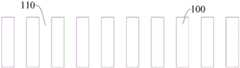
在相关技术中,使用了金属线栅偏光片的显示装置,若欲提高其透光率,通常的做法是减小金属线栅偏光片的占空比,也即减小金属线栅偏光片中金属条的宽度,但金属条的宽度减小之后,金属线栅偏光片极易出现倒伏的不良(参照图1),从而影响其正常的偏光效果。In the related art, in order to improve the light transmittance of a display device using a wire grid polarizer, the usual practice is to reduce the duty cycle of the wire grid polarizer, that is, to reduce the amount of space in the wire grid polarizer. The width of the metal strip, but after the width of the metal strip is reduced, the wire grid polarizer is prone to lodging failure (refer to Figure 1), which affects its normal polarizing effect.
因而,现有的金属线栅偏光片的相关技术仍有待改进。Therefore, the related technology of the existing metal wire grid polarizer still needs to be improved.
发明内容SUMMARY OF THE INVENTION
本发明旨在至少在一定程度上解决相关技术中的技术问题之一。为此,本发明的一个目的在于提出一种金属条不易发生倒伏、透光率高或者偏光效果好的金属线栅偏光片。The present invention aims to solve one of the technical problems in the related art at least to a certain extent. To this end, one object of the present invention is to provide a metal wire grid polarizer that is less prone to lodging of metal strips, has high light transmittance, or has a good polarizing effect.
在本发明的一个方面,本发明提供了一种金属线栅偏光片。根据本发明的实施例,该金属线栅偏光片包括相互平行设置的多个金属条,相邻的两个所述金属条之间具有间隙,还包括:透明防倒伏结构,所述透明防倒伏结构设置在至少一个所述间隙内,并用于支撑所述金属条透明防倒伏结构。该金属线栅偏光片中的金属条不易发生倒伏,且透光率高、偏光效果好。In one aspect of the present invention, the present invention provides a metal wire grid polarizer. According to an embodiment of the present invention, the wire grid polarizer includes a plurality of metal strips arranged in parallel with each other, and there is a gap between two adjacent metal strips, and further includes: a transparent anti-lodging structure, the transparent anti-lodging structure The structure is arranged in at least one of the gaps and is used to support the transparent anti-lodging structure of the metal strip. The metal strips in the metal wire grid polarizer are not prone to lodging, and have high light transmittance and good polarizing effect.
根据本发明的实施例,所述透明防倒伏结构在第一方向上的第一端面和所述金属条在所述第一方向上的第二端面齐平或者基本齐平,其中,所述第一方向为所述金属线栅偏光片的厚度方向。According to an embodiment of the present invention, the first end face of the transparent lodging prevention structure in the first direction is flush or substantially flush with the second end face of the metal strip in the first direction, wherein the first One direction is the thickness direction of the wire grid polarizer.
根据本发明的实施例,所述透明防倒伏结构满足以下条件的至少之一:在所述第一方向上的高度为所述金属条在所述第一方向上高度的三分之一至二分之一;在与所述第一方向垂直,且垂直于相邻的两个所述金属条的第二方向上的宽度为55nm~80nm;材料包括纳米压印胶。According to an embodiment of the present invention, the transparent anti-lodging structure satisfies at least one of the following conditions: the height in the first direction is one third to two times the height of the metal strip in the first direction The width in the second direction perpendicular to the first direction and perpendicular to the two adjacent metal strips is 55 nm to 80 nm; the material includes nano-imprint glue.
根据本发明的实施例,所述透明防倒伏结构设置在全部所述间隙内。According to an embodiment of the present invention, the transparent anti-lodging structure is arranged in all the gaps.
根据本发明的实施例,所述金属线栅偏光片满足以下条件的至少之一:线宽为40nm~50nm;线距为60nm~80nm;厚度为200nm~240nm;透光率不低于46%。According to an embodiment of the present invention, the metal wire grid polarizer satisfies at least one of the following conditions: the line width is 40nm-50nm; the line spacing is 60nm-80nm; the thickness is 200nm-240nm; the light transmittance is not less than 46% .
根据本发明的实施例,所述金属线栅偏光片还包括:衬底,所述透明防倒伏结构的所述第一端面与所述衬底的表面相接触。According to an embodiment of the present invention, the wire grid polarizer further includes: a substrate, and the first end surface of the transparent anti-lodging structure is in contact with a surface of the substrate.
在本发明的另一个方面,本发明提供了一种制作前面所述的金属线栅偏光片的方法。根据本发明的实施例,该方法包括:形成相互平行设置的多个金属条,其中,相邻的两个所述金属条之间具有间隙;形成透明防倒伏结构,所述透明防倒伏结构位于至少一个所述间隙内。该方法操作简单、方便,容易实现,易于工业化生产,且可以有效制作得到前面所述的金属线栅偏光片。In another aspect of the present invention, the present invention provides a method of fabricating the aforementioned wire grid polarizer. According to an embodiment of the present invention, the method includes: forming a plurality of metal strips arranged in parallel with each other, wherein there is a gap between two adjacent metal strips; forming a transparent anti-lodging structure, the transparent anti-lodging structure is located in within at least one of said gaps. The method is simple to operate, convenient, easy to implement, easy to industrialize production, and can effectively manufacture the aforementioned metal wire grid polarizer.
根据本发明的实施例,该方法进一步包括:在衬底的表面上形成多个沿第二方向间隔设置所述透明防倒伏结构;在所述衬底未被所述透明防倒伏结构覆盖的表面上和多个所述透明防倒伏结构远离所述衬底的表面上形成预制金属层;在所述预制金属层远离所述衬底的表面上形成第一刻蚀保护层,所述第一刻蚀保护层在所述衬底上的正投影与所述透明防倒伏结构在所述衬底上的正投影完全不重叠;对所述预制金属层进行刻蚀处理,得到多个所述金属条。According to an embodiment of the present invention, the method further includes: forming a plurality of the transparent anti-lodging structures on the surface of the substrate and spaced along the second direction; and on the surface of the substrate not covered by the transparent anti-lodging structures forming a prefabricated metal layer on the surface of the transparent anti-lodging structure far from the substrate; forming a first etching protection layer on the surface of the prefabricated metal layer far away from the substrate; The orthographic projection of the etching protection layer on the substrate does not overlap with the orthographic projection of the transparent anti-lodging structure on the substrate at all; the prefabricated metal layer is etched to obtain a plurality of the metal strips .
根据本发明的实施例,在形成所述预制金属层之后,形成所述第一刻蚀保护层之前,该方法还包括:在所述预制金属层远离所述衬底的表面上形成整层的第二刻蚀保护层,在形成所述第一刻蚀保护层以后,对所述预制金属层进行所述刻蚀处理时,对未被所述第一刻蚀保护层覆盖的部分所述第二刻蚀保护层也进行所述刻蚀处理。According to an embodiment of the present invention, after forming the prefabricated metal layer and before forming the first etch protection layer, the method further includes: forming a whole-layered metal layer on the surface of the prefabricated metal layer away from the substrate For the second etching protection layer, after the first etching protection layer is formed, when performing the etching process on the prefabricated metal layer, the first etching protection layer is not covered by the first etching protection layer. The second etching protection layer is also subjected to the etching process.
根据本发明的实施例,所述刻蚀处理包括干法刻蚀,在所述干法刻蚀的刻蚀气体中,甲烷的体积百分含量为20%~30%。According to an embodiment of the present invention, the etching process includes dry etching, and in the etching gas for the dry etching, the volume percentage of methane is 20% to 30%.
根据本发明的实施例,所述透明防倒伏结构是通过纳米压印形成的。According to an embodiment of the present invention, the transparent anti-lodging structure is formed by nano-imprinting.
在本发明的又一个方面,本发明提供了一种显示装置。根据本发明的实施例,该显示装置包括前面所述的金属线栅偏光片。该显示装置的显示效果好。In yet another aspect of the present invention, the present invention provides a display device. According to an embodiment of the present invention, the display device includes the aforementioned wire grid polarizer. The display device has a good display effect.
附图说明Description of drawings
图1显示了相关技术中的金属线栅偏光片出现倒伏不良时的扫描电镜照片。FIG. 1 shows a scanning electron microscope photograph of a wire grid polarizer in the related art when poor lodging occurs.
图2显示了本发明一个实施例中的金属线栅偏光片的剖面结构示意图。FIG. 2 shows a schematic cross-sectional structure diagram of a metal wire grid polarizer in an embodiment of the present invention.
图3显示了本发明另一个实施例中的金属线栅偏光片的剖面结构示意图。FIG. 3 shows a schematic cross-sectional structure diagram of a metal wire grid polarizer in another embodiment of the present invention.
图4显示了本发明又一个实施例中的金属线栅偏光片的剖面结构示意图。FIG. 4 shows a schematic cross-sectional structure diagram of a metal wire grid polarizer in another embodiment of the present invention.
图5显示了本发明再一个实施例中的金属线栅偏光片的剖面结构示意图。FIG. 5 shows a schematic cross-sectional structure diagram of a metal wire grid polarizer in still another embodiment of the present invention.
图6显示了本发明一个实施例中的制作金属线栅偏光片的方法的流程示意图。FIG. 6 shows a schematic flowchart of a method for fabricating a wire grid polarizer according to an embodiment of the present invention.
图7a和图7b显示了本发明另一个实施例中的制作金属线栅偏光片的方法的流程示意图。7a and 7b are schematic flowcharts showing a method for fabricating a wire grid polarizer according to another embodiment of the present invention.
图8显示了本发明又一个实施例中的制作金属线栅偏光片的方法的流程示意图。FIG. 8 shows a schematic flowchart of a method for fabricating a wire grid polarizer according to still another embodiment of the present invention.
图9a、图9b、图9c、图9d和图9e显示了本发明再一个实施例中的制作金属线栅偏光片的方法的流程示意图。9a, 9b, 9c, 9d and 9e are schematic flowcharts showing a method for fabricating a wire grid polarizer according to still another embodiment of the present invention.
图10显示了本发明再一个实施例中的制作金属线栅偏光片的方法的流程示意图。FIG. 10 shows a schematic flowchart of a method for fabricating a wire grid polarizer according to still another embodiment of the present invention.
图11a、图11b、图11c和图11d显示了本发明再一个实施例中的制作金属线栅偏光片的方法的流程示意图。11a , 11b , 11c and 11d are schematic flowcharts showing a method for fabricating a wire grid polarizer according to still another embodiment of the present invention.
附图标记:Reference number:
1:第一端面2:第二端面10:金属线栅偏光片51:第一刻蚀保护层52:第二刻蚀保护层53:图案化层99:预制金属层100:金属条110:间隙200:透明防倒伏结构300:衬底1: first end face 2: second end face 10: metal wire grid polarizer 51: first etching protection layer 52: second etching protection layer 53: patterned layer 99: prefabricated metal layer 100: metal strip 110: gap 200: Transparent anti-lodging structure 300: Substrate
具体实施方式Detailed ways
下面详细描述本发明的实施例。下面描述的实施例是示例性的,仅用于解释本发明,而不能理解为对本发明的限制。实施例中未注明具体技术或条件的,按照本领域内的文献所描述的技术或条件或者按照产品说明书进行。所用试剂或仪器未注明生产厂商者,均为可以通过市购获得的常规产品。Embodiments of the present invention are described in detail below. The embodiments described below are exemplary, only for explaining the present invention, and should not be construed as limiting the present invention. If no specific technique or condition is indicated in the examples, the technique or condition described in the literature in the field or the product specification is used. The reagents or instruments used without the manufacturer's indication are conventional products that can be obtained from the market.
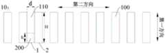
在本发明的一个方面,本发明提供了一种金属线栅偏光片。根据本发明的实施例,参照图2,该金属线栅偏光片10包括相互平行设置的多个金属条100,相邻的两个所述金属条100之间具有间隙110,还包括:透明防倒伏结构200,所述透明防倒伏结构200设置在至少一个所述间隙110内,并用于支撑所述金属条100透明防倒伏结构。由于透明防倒伏结构200对金属条100起到了支撑作用,因而该金属线栅偏光片10中的金属条100不易发生倒伏,从而可以将所述金属条100的宽度减小,同时透明防倒伏结构200本身也是透明的,进而其可以实现较高的透光率、且偏光效果好。In one aspect of the present invention, the present invention provides a metal wire grid polarizer. According to an embodiment of the present invention, referring to FIG. 2 , the
根据本发明的实施例,需要说明的是,金属线栅偏光片10、和其中的金属条100以及透明防倒伏结构200均是三维立体结构,为将术语统一,在本文中,参照图3,定义金属线栅偏光片10的厚度方向为第一方向;与所述第一方向垂直,且垂直于相邻的两个所述金属条100的方向为第二方向(也即金属线栅偏光片10的线宽和线距所在的方向)。According to an embodiment of the present invention, it should be noted that the metal
根据本发明的实施例,在本发明中,透明防倒伏结构200位于间隙110中,只要能够对金属条100起到支撑作用即可,也就是说,透明防倒伏结构200在间隙中的具体设置位置并不必须限定在某一个位置上,只要能够对金属条100起到支撑作用的位置,均应落在本发明的保护范围内。例如,在本发明的一些实施例中,参照图2,透明防倒伏结构200在第一方向上的任何一个端面均不与金属条100在第一方向上的端面齐平或者基本齐平,也就是说,透明防倒伏结构200设置在相邻的两个金属条100的间隙110的中部;当然,在本发明的另一些实施例中,参照图3,所述透明防倒伏结构200在第一方向上的第一端面1和所述金属条100在所述第一方向上的第二端面2也可以是齐平或者基本齐平的。通过此种方式设置的透明防倒伏结构200,其形成工艺较为简单、同时可以对金属条100起到较好的支撑作用。According to the embodiment of the present invention, in the present invention, the transparent
根据本发明的实施例,另外,前已述及,本发明中的透明防倒伏结构200只要能够对金属条100起到支撑作用即可,那么,其在第一方向上的高度也同样是不受特别限制的。然而,进一步地,发明人综合考虑了透明防倒伏结构200对金属条100的支撑作用和金属线栅偏光片10的透光率以及偏光效果,参照图3,当所述透明防倒伏结构200在第一方向上的高度h为所述金属条100在第一方向上高度H的三分之一至二分之一时(具体而言,该数值可以是三分之一至二分之一之间的任意数值,例如0.35、0.38、0.40、0.42、0.44、0.46或者0.48等),金属条100既不容易出现倒伏,同时金属线栅偏光片10的透光率也进一步提高,偏光效果也进一步变好。According to the embodiment of the present invention, in addition, as mentioned above, as long as the transparent
根据本发明的实施例,在本发明中,透明防倒伏结构200位于相邻的两个金属条100之间的间隙110中,而透明防倒伏结构200在第二方向上的宽度d并不一定要恰好等于金属线栅偏光片10的线距S,才能对金属条100起到支撑作用,该宽度d也是可以略小于金属线栅偏光片10的线距S的。当然,本领域技术人员也可以理解,当上述宽度d与金属线栅偏光片10的线距S恰好相等时,其所起到的支撑作用最好。例如,在本发明的一些实施例中,当所述金属线栅偏光片10的线距S为60nm~80nm时,所述透明防倒伏结构200在第二方向上的宽度d可以是55nm~80nm,具体地,其可以是55nm、60nm、65nm、70nm、75nm或者80nm等。According to an embodiment of the present invention, in the present invention, the transparent
根据本发明的实施例,前已述及,透明防倒伏结构200为透明的,其具体材料可以在相关技术中的透明材料中进行灵活选择,更进一步地,透明防倒伏结构200的材料可以包括纳米压印胶。材料包括纳米压印胶的透明防倒伏结构200,其不仅仅透明度高,可以使得金属线栅偏光片10的透光率高,进而偏光效果好;同时,其形成工艺也较为简单、易于实现产业化。当然,本领域技术人员也可以理解,除前面所述的纳米压印胶以外,透明防倒伏结构200的材料也可以是相关技术中的其他材料,在此不再过多赘述。According to the embodiment of the present invention, as mentioned above, the transparent
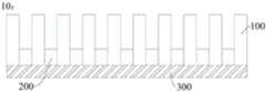
根据本发明的实施例,更进一步地,透明防倒伏结构200不仅是设置在相邻的两个金属条100之间的一个间隙110或者多个间隙110中的,参照图4,其是设置在全部所述间隙110内的。由此,金属线栅偏光片10中的每两个金属条100之间的间隙110中均具有透明防倒伏结构200,可以使得全部的金属条100不易发生倒伏,进而整个金属线栅偏光片10的透光率高、偏光效果优异。According to the embodiment of the present invention, further, the transparent
根据本发明的实施例,设置了本发明的透明防倒伏结构200的金属线栅偏光片10,当其线宽W相较于相关技术中的金属线栅偏光片更窄时,其金属条仍然可以不发生倒伏的不良,本领域技术人员可以理解,当金属线栅偏光片10的线宽W变窄时,相应地,其线距S就会相应更宽。例如,在本发明的一些实施例中,参照图4,所述金属线栅偏光片10的线宽W可以为40nm~50nm,具体地,可以是40nm、42nm、44nm、46nm、48nm或者50nm等;线距S可以为60nm~80nm,具体地,可以是60nm、64nm、68nm、72nm、76nm或者80nm等。由此,该金属线栅偏光片10中的金属条100既不会发生倒伏,且该金属线栅偏光片10的透光率也较高。According to an embodiment of the present invention, when the
根据本发明的实施例,前已述及,设置了本发明的透明防倒伏结构200的金属线栅偏光片10透光率较高,具体而言,发明人经过大量周密的考察和实验验证后发现,本发明所述的金属线栅偏光片10的透光率不低于46%,进一步地,该金属线栅偏光片10的透光率不低于48%。具体而言,该金属线栅偏光片10的透光率可以是50%、52%、54%或者56%等。According to the embodiment of the present invention, as mentioned above, the metal
根据本发明的实施例,设置了本发明所述的透明防倒伏结构200的金属线栅偏光片10可以在实现金属条100不发生倒伏,且透光率较高,偏光效果也较好的前提下,具体较薄的厚度,符合显示装置轻薄化的发展趋势。例如,在本发明的一些实施例中,所述金属线栅偏光片10的厚度可以是200nm~240nm,具体地,可以是200nm、210nm、220nm、230nm或者240nm等。当然,其也可以根据实际所需选用其他厚度,在此不再过多赘述。According to the embodiment of the present invention, the metal
根据本发明的实施例,进一步地,所述金属条100的材料不受特别限制,在本发明的一些实施例中,所述金属条100的材料可以是铝。由此,材料来源广泛、易得,成本较低,且可以较好地实现偏光效果。According to the embodiments of the present invention, further, the material of the
在本发明的另一些实施例中,参照图5,所述金属线栅偏光片10还可以包括:衬底300,所述透明防倒伏结构200的所述第一端面1与所述衬底300的表面相接触。由此,易于形成在第一方向上的第一端面1和所述金属条100在所述第一方向上的第二端面是齐平或者基本齐平的透明防倒伏结构200,工艺简单、易于产业化。In other embodiments of the present invention, referring to FIG. 5 , the
根据本发明的实施例,进一步地,所述衬底300的材料可以根据实际需要进行灵活选择,在本发明的一些实施例中,所述衬底300的材料可以是玻璃。由此,材料来源广泛、易得,成本较低,且可以适用于大多数应用领域,应用范围广泛。According to embodiments of the present invention, further, the material of the
在本发明的另一个方面,本发明提供了一种制作前面所述的金属线栅偏光片的方法。根据本发明的实施例,参照图6和图7a、图7b,该方法可以包括以下步骤:In another aspect of the present invention, the present invention provides a method of fabricating the aforementioned wire grid polarizer. According to an embodiment of the present invention, referring to Fig. 6 and Fig. 7a, Fig. 7b, the method may include the following steps:
S10:形成相互平行设置的多个金属条100,其中,相邻的两个所述金属条100之间具有间隙110(结构示意图参照图7a)。S10 : forming a plurality of
S20:形成透明防倒伏结构200,所述透明防倒伏结构200位于至少一个所述间隙110内(结构示意图参照图7b)。S20 : forming a transparent
根据本发明的实施例,上述形成多个金属条100和所述透明防倒伏结构200的具体工艺,本领域技术人员可以根据实际需要进行灵活选择,在此不再过多赘述,且需要说明的是,所述透明防倒伏结构200和所述金属条100的形成的先后顺序并不受上述描述限制,本领域技术人员可以理解,在本发明的另一些实施例中,也可以是先形成所述防倒伏结构200,再形成所述金属条100。According to the embodiment of the present invention, the above-mentioned specific process for forming the plurality of
在本发明的另一些实施例中,参照图8和图9a、图9b、图9c、图9d、图9e,该方法可以进一步包括以下步骤:In other embodiments of the present invention, referring to Fig. 8 and Fig. 9a, Fig. 9b, Fig. 9c, Fig. 9d, Fig. 9e, the method may further include the following steps:
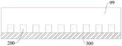
S100:在衬底300的表面上形成多个沿第二方向间隔设置所述透明防倒伏结构200(结构示意图参照图9a)。S100 : forming a plurality of the transparent
根据本发明的实施例,在衬底300的表面上形成多个沿第二方向间隔设置所述透明防倒伏结构200的具体工艺可以是通过纳米压印形成的。具体而言,可以是在所述衬底300的表面上先涂覆一层纳米压印胶,然后对其进行压印处理,从而形成所述透明防倒伏结构200。由此,工艺简单、方便,容易实现,易于工业化生产。According to an embodiment of the present invention, a specific process for forming a plurality of the transparent
S200:在所述衬底300未被所述透明防倒伏结构200覆盖的表面上和多个所述透明防倒伏结构200远离所述衬底300的表面上形成预制金属层99(结构示意图参照图9b)。S200 : forming a
根据本发明的实施例,在所述衬底300未被所述透明防倒伏结构200覆盖的表面上和多个所述透明防倒伏结构200远离所述衬底300的表面上形成预制金属层99的具体工艺可以是磁控溅射。具体而言,可以是在所述表面上直接溅射一层铝,从而形成所述预制金属层99。由此,工艺简单、方便,容易实现,易于工业化生产。According to an embodiment of the present invention, a
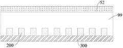
S300:在所述预制金属层99远离所述衬底300的表面上形成第一刻蚀保护层51,所述第一刻蚀保护层51在所述衬底300上的正投影与所述透明防倒伏结构200在所述衬底300上的正投影完全不重叠(结构示意图参照图9c)。S300 : forming a first
根据本发明的实施例,在所述预制金属层99远离所述衬底300的表面上形成第一刻蚀保护层51的具体工艺可以是通过纳米压印形成的。具体而言,可以是在所述表面上先涂覆一层纳米压印胶,然后对其进行压印处理,从而形成所述第一刻蚀保护层51的,也就是说,所述第一刻蚀保护层51的材料也可以是纳米压印胶。由此,工艺简单、方便,容易实现,易于工业化生产,且可以较好地保护预制金属层99上不需要被刻蚀的部分在后续的步骤中不被刻蚀掉,进而形成形貌较好的金属条100。According to an embodiment of the present invention, the specific process of forming the first
S400:对所述预制金属层99进行刻蚀处理,得到多个所述金属条100(结构示意图参照图9d)。S400 : performing etching on the
根据本发明的实施例,对所述预制金属层99进行刻蚀处理的具体工艺可以包括干法刻蚀,在所述干法刻蚀的刻蚀气体中,甲烷的体积百分含量为20%~30%,具体地,可以为20%、25%或者30%等。由于在干法刻蚀中,甲烷起到的作用在于在刻蚀气体中形成多个亚甲基的交联,形成聚合物,可降低金属条100和透明防倒伏结构200的刻蚀选择比。而具有上述体积百分含量的甲烷的刻蚀气体,其中甲烷的含量较低,进而该刻蚀气体所刻蚀的金属条100就会更多更快,从而使得本发明所述的金属线栅偏光片10的线宽W相较于相关技术中的金属线栅偏光片的线宽会更窄,进而提高其透光率。According to the embodiment of the present invention, the specific process of etching the
根据本发明的实施例,另外,本领域技术人员可以理解,在前面所述的刻蚀气体中,还可以包括其他常规的刻蚀气体,例如,氯气可以作为主刻蚀气体;三氯化硼可以是去除金属条表面的钝化层,另外也可以起到侧壁保护的作用,同时调节氯离子的浓度,并在刻蚀时提供向下方向的物理轰击;至于氮气则可以起到侧壁保护的作用,上述各个气体在前面所述的刻蚀气体中的体积百分含量,本领域技术人员可以根据需要进行灵活选择;其刻蚀机理也与相关技术中干法刻蚀的刻蚀机理相同,在此不再过多赘述。According to the embodiment of the present invention, in addition, those skilled in the art can understand that the aforementioned etching gas may also include other conventional etching gases, for example, chlorine gas may be used as the main etching gas; boron trichloride It can be to remove the passivation layer on the surface of the metal strip, and it can also play the role of sidewall protection, adjust the concentration of chloride ions, and provide physical bombardment in the downward direction during etching; as for nitrogen, it can play the role of sidewall. The role of protection, the volume percentage of the above-mentioned gases in the aforementioned etching gas, those skilled in the art can flexibly choose according to their needs; its etching mechanism is also the same as the etching mechanism of dry etching in the related art. The same is not repeated here.
根据本发明的实施例,本领域技术人员可以理解,在对所述预制金属层99进行刻蚀处理,得到多个所述金属条100以后,该方法还可以包括去除所述第一刻蚀保护层51的步骤,从而得到所述金属线栅偏光片10(结构示意图参照图9e),所述第一刻蚀保护层51的具体去除工艺和方式,本领域技术人员可以根据实际需要进行灵活选择,在此不再过多赘述。According to the embodiment of the present invention, those skilled in the art can understand that after the
在本发明的又一些实施例中,更进一步地,参照图10和图11a、图11b、图11c、图11d,在形成所述预制金属层99之后,形成所述第一刻蚀保护层51之前,该方法还可以包括以下步骤:In still other embodiments of the present invention, further, referring to FIG. 10 and FIGS. 11 a , 11 b , 11 c and 11 d , after the
S500:在所述预制金属层99远离所述衬底300的表面上形成整层的第二刻蚀保护层52(结构示意图参照图11a)。S500 : forming a whole second
根据本发明的实施例,在所述预制金属层99远离所述衬底300的表面上形成整层的第二刻蚀保护层52的具体工艺可以是物理气相沉积,其具体工艺条件、参数,本领域技术人员可以根据实际需要进行灵活选择,在此不再过多赘述。由此,工艺简单、方便,容易实现,易于工业化生产,且可以使得所述预制金属层99远离所述衬底300的表面在后续步骤中不至于由于接触刻蚀气体的时间过长而刻蚀得过多,进而导致制作得到的金属线栅偏光片10的金属条100的不同部位的宽度不均匀,从而影响偏光效果。According to an embodiment of the present invention, the specific process for forming the entire second
根据本发明的实施例,进一步地,所述第二刻蚀保护层52的材料可以是氧化硅,其厚度可以是60μm~100μm,具体地,可以是60μm、70μm、80μm、90μm或者100μm等。由此,材料来源广泛、易得,成本较低,且可以较好地实现上述防止过刻的效果。According to an embodiment of the present invention, further, the material of the second
根据本发明的实施例,更进一步地,在本实施例中,后续步骤中在形成所述第一刻蚀保护层51以后(结构示意图参照图11b),对所述预制金属层99进行所述刻蚀处理时,对未被所述第一刻蚀保护层51覆盖的部分所述第二刻蚀保护层52也进行所述刻蚀处理(结构示意图参照图11c),经过所述刻蚀处理的第二刻蚀保护层52形成图案化层53。最后,本领域技术人员可以理解,在得到多个所述金属条100以后,该方法还可以包括去除所述第一刻蚀保护层51和图案化层53的步骤,从而得到所述金属线栅偏光片10(结构示意图参照图11d),所述第一刻蚀保护层51和图案化层53的具体去除工艺和方式,本领域技术人员可以根据实际需要进行灵活选择,在此不再过多赘述。According to an embodiment of the present invention, further, in this embodiment, after the first
在本发明的又一个方面,本发明提供了一种显示装置。根据本发明的实施例,该显示装置包括前面所述的金属线栅偏光片。该显示装置的显示效果好。In yet another aspect of the present invention, the present invention provides a display device. According to an embodiment of the present invention, the display device includes the aforementioned wire grid polarizer. The display device has a good display effect.
根据本发明的实施例,该显示装置除前面所述的金属线栅偏光片以外,还包括其他必要的结构和组成,例如显示背板等,本领域技术人员可根据显示装置的具体种类和使用要求进行补充和设计,在此不再过多赘述。According to an embodiment of the present invention, in addition to the aforementioned metal wire grid polarizer, the display device also includes other necessary structures and components, such as a display backplane, etc. Those skilled in the art can use the specific type and use of the display device according to Supplements and designs are required, and will not be repeated here.
根据本发明的实施例,该显示装置的具体种类不受特别限制,例如包括但不限于手机、平板电脑、可穿戴设备、游戏机等。According to the embodiment of the present invention, the specific type of the display device is not particularly limited, for example, it includes but is not limited to a mobile phone, a tablet computer, a wearable device, a game console, and the like.
在本发明的描述中,需要理解的是,术语“第一”、“第二”仅用于描述目的,而不能理解为指示或暗示相对重要性或者隐含指明所指示的技术特征的数量。由此,限定有“第一”、“第二”的特征可以明示或者隐含地包括一个或者更多个该特征。在本发明的描述中,“多个”的含义是两个或两个以上,除非另有明确具体的限定。In the description of the present invention, it should be understood that the terms "first" and "second" are only used for description purposes, and cannot be interpreted as indicating or implying relative importance or the number of indicated technical features. Thus, a feature defined as "first" or "second" may expressly or implicitly include one or more of that feature. In the description of the present invention, "plurality" means two or more, unless otherwise expressly and specifically defined.
在本说明书的描述中,参考术语“一个实施例”、“一些实施例”、“示例”、“具体示例”、或“一些示例”等的描述意指结合该实施例或示例描述的具体特征、结构、材料或者特点包含于本发明的至少一个实施例或示例中。在本说明书中,对上述术语的示意性表述不必须针对的是相同的实施例或示例。而且,描述的具体特征、结构、材料或者特点可以在任一个或多个实施例或示例中以合适的方式结合。此外,在不相互矛盾的情况下,本领域的技术人员可以将本说明书中描述的不同实施例或示例以及不同实施例或示例的特征进行结合和组合。In the description of this specification, description with reference to the terms "one embodiment," "some embodiments," "example," "specific example," or "some examples", etc., mean specific features described in connection with the embodiment or example , structure, material or feature is included in at least one embodiment or example of the present invention. In this specification, schematic representations of the above terms are not necessarily directed to the same embodiment or example. Furthermore, the particular features, structures, materials or characteristics described may be combined in any suitable manner in any one or more embodiments or examples. Furthermore, those skilled in the art may combine and combine the different embodiments or examples described in this specification, as well as the features of the different embodiments or examples, without conflicting each other.
尽管上面已经示出和描述了本发明的实施例,可以理解的是,上述实施例是示例性的,不能理解为对本发明的限制,本领域的普通技术人员在本发明的范围内可以对上述实施例进行变化、修改、替换和变型。Although the embodiments of the present invention have been shown and described above, it should be understood that the above-mentioned embodiments are exemplary and should not be construed as limiting the present invention. Embodiments are subject to variations, modifications, substitutions and variations.
Claims (12)
Priority Applications (1)
| Application Number | Priority Date | Filing Date | Title |
|---|---|---|---|
| CN202010541763.2ACN111562643A (en) | 2020-06-15 | 2020-06-15 | Wire grid polarizer and its manufacturing method and display device |
Applications Claiming Priority (1)
| Application Number | Priority Date | Filing Date | Title |
|---|---|---|---|
| CN202010541763.2ACN111562643A (en) | 2020-06-15 | 2020-06-15 | Wire grid polarizer and its manufacturing method and display device |
Publications (1)
| Publication Number | Publication Date |
|---|---|
| CN111562643Atrue CN111562643A (en) | 2020-08-21 |
Family
ID=72070256
Family Applications (1)
| Application Number | Title | Priority Date | Filing Date |
|---|---|---|---|
| CN202010541763.2APendingCN111562643A (en) | 2020-06-15 | 2020-06-15 | Wire grid polarizer and its manufacturing method and display device |
Country Status (1)
| Country | Link |
|---|---|
| CN (1) | CN111562643A (en) |
Cited By (2)
| Publication number | Priority date | Publication date | Assignee | Title |
|---|---|---|---|---|
| CN111679356A (en)* | 2020-06-22 | 2020-09-18 | 京东方科技集团股份有限公司 | Polarizing plate and preparation method thereof |
| WO2022178769A1 (en)* | 2021-02-25 | 2022-09-01 | 京东方科技集团股份有限公司 | Polarizer and manufacturing method therefor, display panel and display apparatus |
Citations (3)
| Publication number | Priority date | Publication date | Assignee | Title |
|---|---|---|---|---|
| JPH03103802A (en)* | 1989-09-07 | 1991-04-30 | Max Planck Ges Foerderung Wissenschaft Ev | Infrared polarizer |
| CN105683816A (en)* | 2013-10-24 | 2016-06-15 | 莫克斯泰克公司 | Polarizer with wire pair over rib |
| CN106575054A (en)* | 2014-08-14 | 2017-04-19 | 应用材料公司 | Systems, apparatus and methods for optical polarizers for electromagnetic interference shielding |
- 2020
- 2020-06-15CNCN202010541763.2Apatent/CN111562643A/enactivePending
Patent Citations (3)
| Publication number | Priority date | Publication date | Assignee | Title |
|---|---|---|---|---|
| JPH03103802A (en)* | 1989-09-07 | 1991-04-30 | Max Planck Ges Foerderung Wissenschaft Ev | Infrared polarizer |
| CN105683816A (en)* | 2013-10-24 | 2016-06-15 | 莫克斯泰克公司 | Polarizer with wire pair over rib |
| CN106575054A (en)* | 2014-08-14 | 2017-04-19 | 应用材料公司 | Systems, apparatus and methods for optical polarizers for electromagnetic interference shielding |
Cited By (2)
| Publication number | Priority date | Publication date | Assignee | Title |
|---|---|---|---|---|
| CN111679356A (en)* | 2020-06-22 | 2020-09-18 | 京东方科技集团股份有限公司 | Polarizing plate and preparation method thereof |
| WO2022178769A1 (en)* | 2021-02-25 | 2022-09-01 | 京东方科技集团股份有限公司 | Polarizer and manufacturing method therefor, display panel and display apparatus |
Similar Documents
| Publication | Publication Date | Title |
|---|---|---|
| JP6454613B2 (en) | Mask blank, phase shift mask manufacturing method, phase shift mask, and semiconductor device manufacturing method | |
| US20200150524A1 (en) | Mask blank, transfer mask, method for manufacturing transfer mask, and method for manufacturing semiconductor device | |
| CN111562643A (en) | Wire grid polarizer and its manufacturing method and display device | |
| CN103839781A (en) | Method for forming fine patterns on semiconductor | |
| JP2009105252A (en) | Manufacturing method for fine pattern, and optical element | |
| TW200908093A (en) | Method for fabricating semiconductor device | |
| CN101738846A (en) | Mask plate and manufacture method thereof | |
| JP5661973B2 (en) | Method for manufacturing phase shift mask | |
| US20160202613A1 (en) | Graphene sensor and method of fabricating the same and touch-sensitive display device | |
| CN104425225A (en) | Forming method for triple graphs | |
| JP5917020B2 (en) | Manufacturing method of mask blank and multi-tone mask | |
| US20090170310A1 (en) | Method of forming a metal line of a semiconductor device | |
| CN108305881B (en) | Array substrate, manufacturing method thereof, display panel and display device | |
| CN109917503B (en) | A grating device, its manufacturing method, and a display device | |
| JP5421380B2 (en) | mold | |
| TW202303261A (en) | Mask blank, phase shift mask, and method for manufacturing semiconductor device | |
| CN104216233A (en) | Exposure method | |
| CN113835545B (en) | Optical mask and electronic device | |
| CN108062001A (en) | The patterning method of film layer, wire grating polarization structure and preparation method thereof | |
| CN108132496B (en) | Metal gate polarizer, manufacturing method thereof, liquid crystal panel and liquid crystal display | |
| CN102856190B (en) | Etching method for strip-type structure | |
| EP3112934A2 (en) | Inorganic material film, photomask blank, and method for manufacturing photomask | |
| CN207924332U (en) | Array substrate, display panel and display device | |
| TW202101580A (en) | Method of line roughness improvement by plasma selective deposition | |
| JP6206667B2 (en) | Pattern formation method |
Legal Events
| Date | Code | Title | Description |
|---|---|---|---|
| PB01 | Publication | ||
| PB01 | Publication | ||
| SE01 | Entry into force of request for substantive examination | ||
| SE01 | Entry into force of request for substantive examination | ||
| RJ01 | Rejection of invention patent application after publication | ||
| RJ01 | Rejection of invention patent application after publication | Application publication date:20200821 |