CN111527538A - Data Shift Circuits for Current Mode Displays - Google Patents
Data Shift Circuits for Current Mode DisplaysDownload PDFInfo
- Publication number
- CN111527538A CN111527538ACN201880084774.3ACN201880084774ACN111527538ACN 111527538 ACN111527538 ACN 111527538ACN 201880084774 ACN201880084774 ACN 201880084774ACN 111527538 ACN111527538 ACN 111527538A
- Authority
- CN
- China
- Prior art keywords
- data
- digital data
- emitters
- transmitter
- output
- Prior art date
- Legal status (The legal status is an assumption and is not a legal conclusion. Google has not performed a legal analysis and makes no representation as to the accuracy of the status listed.)
- Pending
Links
Images


Classifications
- G—PHYSICS
- G09—EDUCATION; CRYPTOGRAPHY; DISPLAY; ADVERTISING; SEALS
- G09G—ARRANGEMENTS OR CIRCUITS FOR CONTROL OF INDICATING DEVICES USING STATIC MEANS TO PRESENT VARIABLE INFORMATION
- G09G3/00—Control arrangements or circuits, of interest only in connection with visual indicators other than cathode-ray tubes
- G09G3/02—Control arrangements or circuits, of interest only in connection with visual indicators other than cathode-ray tubes by tracing or scanning a light beam on a screen
- G09G3/025—Control arrangements or circuits, of interest only in connection with visual indicators other than cathode-ray tubes by tracing or scanning a light beam on a screen with scanning or deflecting the beams in two directions or dimensions
- G—PHYSICS
- G11—INFORMATION STORAGE
- G11C—STATIC STORES
- G11C13/00—Digital stores characterised by the use of storage elements not covered by groups G11C11/00, G11C23/00, or G11C25/00
- G11C13/04—Digital stores characterised by the use of storage elements not covered by groups G11C11/00, G11C23/00, or G11C25/00 using optical elements ; using other beam accessed elements, e.g. electron or ion beam
- G—PHYSICS
- G11—INFORMATION STORAGE
- G11C—STATIC STORES
- G11C19/00—Digital stores in which the information is moved stepwise, e.g. shift registers
- G11C19/18—Digital stores in which the information is moved stepwise, e.g. shift registers using capacitors as main elements of the stages
- G11C19/182—Digital stores in which the information is moved stepwise, e.g. shift registers using capacitors as main elements of the stages in combination with semiconductor elements, e.g. bipolar transistors, diodes
- G11C19/184—Digital stores in which the information is moved stepwise, e.g. shift registers using capacitors as main elements of the stages in combination with semiconductor elements, e.g. bipolar transistors, diodes with field-effect transistors, e.g. MOS-FET
- G—PHYSICS
- G11—INFORMATION STORAGE
- G11C—STATIC STORES
- G11C19/00—Digital stores in which the information is moved stepwise, e.g. shift registers
- G11C19/28—Digital stores in which the information is moved stepwise, e.g. shift registers using semiconductor elements
- G—PHYSICS
- G11—INFORMATION STORAGE
- G11C—STATIC STORES
- G11C19/00—Digital stores in which the information is moved stepwise, e.g. shift registers
- G11C19/30—Digital stores in which the information is moved stepwise, e.g. shift registers using opto-electronic devices, i.e. light-emitting and photoelectric devices electrically- or optically-coupled
- G—PHYSICS
- G11—INFORMATION STORAGE
- G11C—STATIC STORES
- G11C19/00—Digital stores in which the information is moved stepwise, e.g. shift registers
- G11C19/34—Digital stores in which the information is moved stepwise, e.g. shift registers using storage elements with more than two stable states represented by steps, e.g. of voltage, current, phase, frequency
- G—PHYSICS
- G09—EDUCATION; CRYPTOGRAPHY; DISPLAY; ADVERTISING; SEALS
- G09G—ARRANGEMENTS OR CIRCUITS FOR CONTROL OF INDICATING DEVICES USING STATIC MEANS TO PRESENT VARIABLE INFORMATION
- G09G2310/00—Command of the display device
- G09G2310/02—Addressing, scanning or driving the display screen or processing steps related thereto
- G09G2310/0264—Details of driving circuits
- G09G2310/0286—Details of a shift registers arranged for use in a driving circuit
- G—PHYSICS
- G09—EDUCATION; CRYPTOGRAPHY; DISPLAY; ADVERTISING; SEALS
- G09G—ARRANGEMENTS OR CIRCUITS FOR CONTROL OF INDICATING DEVICES USING STATIC MEANS TO PRESENT VARIABLE INFORMATION
- G09G2320/00—Control of display operating conditions
- G09G2320/06—Adjustment of display parameters
- G09G2320/0693—Calibration of display systems
Landscapes
- Engineering & Computer Science (AREA)
- Microelectronics & Electronic Packaging (AREA)
- Physics & Mathematics (AREA)
- Computer Hardware Design (AREA)
- General Physics & Mathematics (AREA)
- Theoretical Computer Science (AREA)
- Power Engineering (AREA)
- Control Of Indicators Other Than Cathode Ray Tubes (AREA)
Abstract
Description
Translated fromChinese背景background
在某些类型的显示系统中,有时需要控制不同的光发射器来产生相同的输出。例如,相同的颜色和/或强度可以由不同的发射器在连续的时钟周期或图像帧中输出。如果每个发射器的输入是独立产生的,那么向发射器提供输入的数据带宽会变得非常高。在某些情况下,数据带宽可能超过显示系统所能支持的范围,因此数据不能足够快地输入到发射器,以允许显示器按预期运行。In some types of display systems, it is sometimes necessary to control different light emitters to produce the same output. For example, the same color and/or intensity may be output by different emitters in successive clock cycles or image frames. If the input to each transmitter is generated independently, the data bandwidth to provide the input to the transmitter can become very high. In some cases, the data bandwidth may exceed what the display system can support, so the data cannot be fed into the transmitter fast enough to allow the display to function as expected.
简要概述Brief overview
本公开涉及通过在光发射器之间移位输入数据来控制包括多个光发射器的显示器的技术。本文描述的技术能够结合显示器的操作有效地传输输入数据。描述了各种数据移位布置,包括模拟电路实现和数字电路实现。本文描述的实施例可以以各种组合使用。例如,数字数据移位器可以与模拟发射器电路结合使用,或者与数字发射器电路结合使用。因此,本文描述的组合应被视为说明性的。The present disclosure relates to techniques for controlling a display including multiple light emitters by shifting input data among the light emitters. The techniques described herein can efficiently transmit input data in conjunction with the operation of the display. Various data shifting arrangements are described, including analog circuit implementations and digital circuit implementations. The embodiments described herein can be used in various combinations. For example, digital data shifters may be used in conjunction with analog transmitter circuits, or in conjunction with digital transmitter circuits. Accordingly, the combinations described herein should be considered illustrative.
描述了用于操作包括排列在至少一列中的发射器阵列的显示器的技术。在某些实施例中,数据移位电路将数字数据或其模拟表示存储在第一存储元件中。数据移位电路可以例如使用多路复用器将数字数据或模拟表示多次输出到显示驱动器电路。第一存储元件可以是移位寄存器或电容器。在某些实施例中,数字数据可以在输出到显示驱动器电路之前在数据移位电路内被例如通过多个移位寄存器内部移位。在某些实施例中,模拟表示可以在没有内部移位的情况下从同一电容器存储和读取。Techniques are described for operating a display that includes an array of emitters arranged in at least one column. In some embodiments, the data shift circuit stores digital data or an analog representation thereof in the first storage element. The data shift circuit may output the digital data or analog representation multiple times to the display driver circuit, eg, using a multiplexer. The first storage element may be a shift register or a capacitor. In some embodiments, the digital data may be shifted within a data shift circuit, eg, through a plurality of shift registers, before being output to the display driver circuit. In some embodiments, the analog representation can be stored and read from the same capacitor without internal shifting.
在某些实施例中,显示系统包括发射器阵列、显示驱动器电路和数据移位电路。发射器阵列包括排列成一列的多个发射器。显示驱动器电路被配置成单独驱动多个发射器。数据移位电路包括多个存储元件和多路复用器。数据移位电路被配置为:将数字数据或数字数据的模拟表示存储到多个存储元件中的第一存储元件中;并将数字数据或模拟表示从多路复用器输出到显示驱动器电路。数字数据或模拟表示被输出多次。每次从多路复用器输出数字数据或模拟表示时,显示驱动器电路使用数字数据或模拟表示来驱动多个发射器中的不同发射器。In some embodiments, a display system includes an array of emitters, a display driver circuit, and a data shift circuit. The transmitter array includes a plurality of transmitters arranged in a column. The display driver circuit is configured to drive the plurality of transmitters individually. The data shift circuit includes a plurality of storage elements and a multiplexer. The data shift circuit is configured to: store the digital data or an analog representation of the digital data in a first storage element of the plurality of storage elements; and output the digital data or the analog representation from the multiplexer to the display driver circuit. Digital data or analog representations are output multiple times. Each time the digital data or analog representation is output from the multiplexer, the display driver circuit uses the digital data or analog representation to drive a different one of the multiple transmitters.
在某些实施例中,用于驱动显示器中多个发射器的数据移位电路包括多个存储元件和多路复用器。多个存储元件包括被配置成存储数字数据或数字数据的模拟表示的第一存储元件。多路复用器被配置为多次向显示驱动器电路输出数字数据或模拟表示。每次从多路复用器输出数字数据或模拟表示时,显示驱动器电路使用数字数据或模拟表示来驱动多个发射器中的不同发射器。In some embodiments, a data shift circuit for driving multiple transmitters in a display includes multiple storage elements and a multiplexer. The plurality of storage elements include a first storage element configured to store digital data or an analog representation of digital data. The multiplexer is configured to output digital data or an analog representation to the display driver circuit multiple times. Each time the digital data or analog representation is output from the multiplexer, the display driver circuit uses the digital data or analog representation to drive a different one of the multiple transmitters.
在某些实施例中,显示系统包括发射器阵列、显示驱动器电路、扫描组件和数据移位电路。发射器阵列包括排列成列的多个发射器,其中多个发射器具有相同的颜色。显示驱动器电路被配置成使用数字数据值或数字数据值的模拟表示来单独驱动多个发射器。扫描组件包括接收来自发射器阵列的光的反射表面,扫描组件通过与多个发射器的驱动同步地旋转反射表面来形成输出图像。数据移位电路与发射器阵列分开定位,并且包括多个存储元件,该多个存储元件共同为整个列提供存储。数据移位电路被配置为:接收数字数据或数字数据的模拟表示;将数字数据或模拟表示存储到多个存储元件的第一存储元件中;并将数字数据或模拟表示多次输出到显示驱动器电路。对于多个发射器中的每个发射器,数字数据或模拟表示被输出一次。每次输出数字数据或模拟表示时,显示驱动器电路使用数字数据或模拟表示来驱动不同的发射器,使得随着时间的推移,使用数字数据或模拟表示来驱动多个发射器中的每个发射器。In some embodiments, a display system includes an array of emitters, a display driver circuit, a scan component, and a data shift circuit. The emitter array includes a plurality of emitters arranged in a column, wherein the plurality of emitters have the same color. The display driver circuit is configured to individually drive the plurality of transmitters using the digital data values or analog representations of the digital data values. A scanning assembly includes a reflective surface that receives light from the array of emitters, and the scanning assembly forms an output image by rotating the reflective surface in synchronization with actuation of the plurality of emitters. The data shift circuit is located separately from the transmitter array and includes a plurality of storage elements that together provide storage for the entire column. The data shift circuit is configured to: receive the digital data or an analog representation of the digital data; store the digital data or the analog representation in a first storage element of the plurality of storage elements; and output the digital data or the analog representation multiple times to the display driver circuit. The digital data or analog representation is output once for each of the multiple transmitters. Each time the digital data or analog representation is output, the display driver circuit uses the digital data or analog representation to drive a different transmitter such that each of the multiple transmitters is driven with the digital data or analog representation over time device.
附图简述Brief Description of Drawings
参考以下附图描述说明性实施例。Illustrative embodiments are described with reference to the following figures.
图1示出了用于实现一个或更多个实施例的波导组件。Figure 1 illustrates a waveguide assembly for implementing one or more embodiments.
图2是用于实现一个或更多个实施例的包括扫描显示器的显示系统的简化框图。2 is a simplified block diagram of a display system including a scanning display for implementing one or more embodiments.
图3示出了图2的扫描显示器的操作。FIG. 3 illustrates the operation of the scanning display of FIG. 2 .
图4A至图4E示出了根据实施例的图像数据从扫描显示器到用户的眼睛上的移位。4A-4E illustrate the displacement of image data from a scanning display onto a user's eye, according to an embodiment.
图5是根据实施例的显示系统的高级框图。5 is a high-level block diagram of a display system according to an embodiment.
图6是根据实施例的包括数据移位元件的显示系统的简化框图。6 is a simplified block diagram of a display system including a data shift element, according to an embodiment.
图7是根据实施例的模拟发射器单元的电路图。7 is a circuit diagram of an analog transmitter unit according to an embodiment.
图8是根据实施例的数字发射器单元的电路图。8 is a circuit diagram of a digital transmitter unit according to an embodiment.
图9是根据实施例的包括数据移位部件的模拟发射器单元的电路图。9 is a circuit diagram of an analog transmitter unit including data shifting components, according to an embodiment.
图10示出了根据实施例的两个模拟发射器单元之间的数据移位。Figure 10 illustrates data shifting between two analog transmitter units according to an embodiment.
图11示出了用于实现一个或更多个实施例的具有幻像发射器(phantom emitter)的发射器布局。11 illustrates an emitter layout with phantom emitters for implementing one or more embodiments.
图12示出了根据实施例的模拟幻像单元。Figure 12 shows a simulated phantom unit according to an embodiment.
图13示出了根据实施例的两个模拟发射器单元和一个幻像单元的布置。Figure 13 shows an arrangement of two analog transmitter units and one phantom unit according to an embodiment.
图14示出了根据实施例的两个模拟发射器单元和一个幻像单元的布置。Figure 14 shows an arrangement of two analog transmitter units and one phantom unit according to an embodiment.
图15示出了根据实施例的具有数据移位部件的数字发射器单元和数字幻像单元。Figure 15 shows a digital transmitter unit and a digital phantom unit with data shifting components, according to an embodiment.
图16示出了根据实施例的基于锁存器的发射器和幻像单元。16 illustrates a latch-based transmitter and phantom unit according to an embodiment.
图17是根据实施例的双向数据移位电路的简化框图。17 is a simplified block diagram of a bidirectional data shift circuit according to an embodiment.
图18是根据实施例的包括数字数据移位部件的显示系统的简化框图。18 is a simplified block diagram of a display system including digital data shifting components, according to an embodiment.
图19是根据实施例的包括模拟数据移位部件的显示系统的简化框图。19 is a simplified block diagram of a display system including analog data shifting components, according to an embodiment.
图20是根据实施例的具有反馈收集能力的显示系统的简化框图。20 is a simplified block diagram of a display system with feedback collection capabilities, according to an embodiment.
图21是根据实施例的用于校准驱动电路的方法的流程图。21 is a flowchart of a method for calibrating a driver circuit, according to an embodiment.
附图仅出于说明的目的描绘了本公开的实施例。本领域技术人员将从以下描述中容易地认识到,在不背离本公开的原理或所推崇的优点的情况下,可以采用所示结构和方法的替代实施例。The drawings depict embodiments of the present disclosure for purposes of illustration only. Those skilled in the art will readily recognize from the following description that alternative embodiments of the structures and methods shown may be employed without departing from the principles of the present disclosure or the advantages appreciated.
在附图中,类似的部件和/或特征可以具有相同的参考标签。此外,相同类型的各种部件可以通过在参考标签之后跟随破折号和在相似部件之间进行区分的第二标签来区分。如果在说明书中仅使用第一参考标签,则该描述适用于具有相同第一参考标签的任何一个类似部件,而不管第二参考标签如何。In the drawings, similar components and/or features may have the same reference labels. Furthermore, various components of the same type may be distinguished by following the reference label with a dash and a second label that distinguishes between similar components. If only the first reference label is used in the description, the description applies to any one similar component having the same first reference label, regardless of the second reference label.
在附图中,为了方便起见,已经应用了某些命名惯例,例如字母“M”后跟数字来标识电路中的特定晶体管,或者字母“C”后跟数字来标识电路中的特定电容器。相同的文本标签可以应用于不同的部件。为了清楚起见,在适当的地方添加了参考数字。例如,一个图中的M1可以指与另一个图中的M1不同的晶体管,除非两个M1都标有相同的参考数字。In the drawings, certain naming conventions have been applied for convenience, such as the letter "M" followed by a number to identify a particular transistor in a circuit, or the letter "C" followed by a number to identify a particular capacitor in a circuit. The same text label can be applied to different widgets. Reference numerals have been added where appropriate for clarity. For example, M1 in one figure may refer to a different transistor than M1 in another figure, unless both M1s are marked with the same reference number.
本文使用的术语“行”和“列”是指发射器和/或发射器相关电路成组的物理布置,并且有时一起用于区分彼此正交的两个空间维度。行和列通常是可互换的,不应该被认为是指任何特定的维度。例如,行可以指显示设备的水平或垂直维度。The terms "row" and "column" as used herein refer to the physical arrangement of groups of transmitters and/or transmitter-related circuits, and are sometimes used together to distinguish two spatial dimensions that are orthogonal to each other. Rows and columns are generally interchangeable and should not be considered to refer to any particular dimension. For example, a row may refer to the horizontal or vertical dimension of a display device.
本文使用的术语“单元”是指形成包括单元的多个实例的更复杂电路的构建块的电路。例如,每个发射器可以与包括用于驱动发射器的电路的相应发射器单元配对。The term "cell" as used herein refers to a circuit that forms a building block of a more complex circuit comprising multiple instances of a cell. For example, each transmitter may be paired with a corresponding transmitter unit that includes circuitry for driving the transmitter.
详细描述Detailed Description
在以下描述中,出于解释的目的,阐述了具体细节,以便提供对某些发明实施例的透彻理解。然而,将明显的是,没有这些具体细节也可以实施各种实施例。附图和描述不旨在是限制性的。In the following description, for purposes of explanation, specific details are set forth in order to provide a thorough understanding of certain inventive embodiments. It will be apparent, however, that various embodiments may be practiced without these specific details. The drawings and description are not intended to be limiting.
示例实施例涉及用于通过在光发射器之间移位输入数据来控制包括多个光发射器的显示器的技术。描述了各种数据移位布置,包括模拟电路实现和数字电路实现。本文描述的实施例可以以各种组合使用。例如,数字数据移位器可以与模拟发射器电路结合使用,或者与数字发射器电路结合使用。因此,本文描述的组合应被视为说明性的。Example embodiments relate to techniques for controlling a display including multiple light emitters by shifting input data among the light emitters. Various data shifting arrangements are described, including analog circuit implementations and digital circuit implementations. The embodiments described herein can be used in various combinations. For example, digital data shifters may be used in conjunction with analog transmitter circuits, or in conjunction with digital transmitter circuits. Accordingly, the combinations described herein should be considered illustrative.
在某些实施例中,显示系统包括反馈布置,用于收集关于驱动电路、数据移位电路和/或发射器本身的操作状态或健康状况的反馈。反馈是通过可配置的反馈路径收集的,并且可以包括电压和/或电流测量。在一些实施例中,通过使测试值移位通过发射器电路的整个列以便获得指示该列的整体健康状况的测量结果来收集反馈。In some embodiments, the display system includes a feedback arrangement for collecting feedback on the operational status or health of the driver circuit, the data shift circuit and/or the transmitter itself. Feedback is collected through a configurable feedback path and can include voltage and/or current measurements. In some embodiments, feedback is collected by shifting test values through an entire column of transmitter circuits in order to obtain a measurement indicative of the overall health of the column.
本发明的实施例可以包括人工现实系统或者结合人工现实系统来实现。人工现实是一种在呈现给用户之前已经以某种方式进行了调整的现实形式,其可以包括例如虚拟现实(VR)、增强现实(AR)、混合现实(MR)、混杂现实或其某种组合和/或衍生物。人工现实内容可以包括完全生成的内容或者与捕获的(例如,真实世界的)内容相结合的生成的内容。人工现实内容可以包括视频、音频、触觉反馈或它们的某种组合,并且它们中的任何一个都可以在单个通道或多个通道中呈现(例如向观看者产生三维效果的立体视频)。此外,在一些实施例中,人工现实还可以与应用、产品、附件、服务或其某种组合相关联,这些应用、产品、附件、服务或其某种组合用于例如在人工现实中创建内容和/或在人工现实中以其他方式使用(例如在人工现实中执行活动)。提供人工现实内容的人工现实系统可以在各种平台上实现,这些平台包括连接到主计算机系统的头戴式显示器(HMD)、独立的HMD、移动设备或计算系统、或者能够向一个或更多个观看者提供人工现实内容的任何其他硬件平台。Embodiments of the present invention may include or be implemented in conjunction with an artificial reality system. Artificial reality is a form of reality that has been adjusted in some way before being presented to the user, which can include, for example, Virtual Reality (VR), Augmented Reality (AR), Mixed Reality (MR), Hybrid Reality or some of these Combinations and/or Derivatives. Artificial reality content may include fully generated content or generated content combined with captured (eg, real-world) content. Artificial reality content may include video, audio, haptic feedback, or some combination thereof, and any of these may be presented in a single channel or multiple channels (eg, stereoscopic video that produces a three-dimensional effect to the viewer). Additionally, in some embodiments, the artificial reality may also be associated with applications, products, accessories, services, or some combination thereof, which are used, for example, to create content in the artificial reality and/or otherwise used in artificial reality (eg, performing activities in artificial reality). Artificial reality systems that provide artificial reality content can be implemented on a variety of platforms, including head-mounted displays (HMDs) connected to a host computer system, stand-alone HMDs, mobile devices or computing systems, or capable of reporting to one or more Any other hardware platform that provides artificial reality content to a viewer.
示例实施例总体上涉及用于结合显示器的操作来移位数据的技术。在一些实施例中,显示器是扫描显示器,其通过使用扫描组件(例如,旋转扫描镜或某个其他反射表面)扫描显示图像来为HMD用户生成输出图像。扫描可以在一个或更多个方向上(例如,沿着显示行和/或显示列),并且可以一次覆盖一个或更多个行/列(例如,每种颜色多个行)。扫描可用于形成比物理显示器更大的输出图像和/或具有与物理显示器不同的分辨率的输出图像。如将要解释的,可以通过将相同的图像数据沿着一行或一列移位以使同一行/列中的下一个发射器产生与前一个发射器相同的光输出来操作扫描显示器。以这种方式移位图像数据的一个实际应用是使用来自多个发射器的贡献来生成输出图像的单个像素。可以使用扫描装置将不同发射器的输出映射到输出图像中的相同空间位置。如果扫描执行得足够快,用户将感知发射器的输出为单个单元,例如,通过对单独的发射器的强度进行积分。Example embodiments generally relate to techniques for shifting data in conjunction with operation of a display. In some embodiments, the display is a scanning display that generates an output image for the HMD user by scanning the display image using a scanning component (eg, a rotating scanning mirror or some other reflective surface). Scanning can be in one or more directions (eg, along display rows and/or display columns), and can cover one or more rows/columns at a time (eg, multiple rows per color). Scanning can be used to form an output image that is larger than the physical display and/or has a different resolution than the physical display. As will be explained, a scanning display can be operated by shifting the same image data along a row or column so that the next emitter in the same row/column produces the same light output as the previous emitter. One practical application for shifting image data in this way is to use contributions from multiple emitters to generate a single pixel of an output image. A scanning device can be used to map the outputs of different emitters to the same spatial location in the output image. If the scan is performed fast enough, the user will perceive the output of the transmitter as a single unit, eg, by integrating the intensities of the individual transmitters.
结合电流模式显示器(即,其中发射器使用输入电流来驱动的显示器)来描述示例实施例。然而,本文描述的数据移位技术可以容易地适用于电压控制的显示器。Example embodiments are described in conjunction with current mode displays (ie, displays in which the transmitter is driven using an input current). However, the data shifting techniques described herein can be readily adapted to voltage controlled displays.
扫描显示器中的数据移位Data shift in scan display
图1示出了用于实现一个或更多个实施例的波导组件100。在一些实施例中,波导组件100是近眼显示器(NED)(例如HMD)的部件。波导组件100包括扫描显示器110、输出波导120和控制器130。出于说明的目的,图1示出了与单眼190相关联的波导组件100,但是在一些实施例中,与波导组件100分离(或部分分离)的另一个波导组件向用户的另一只眼睛提供图像光。在部分分离的系统中,一个或更多个部件可以在每只眼睛的波导组件之间共享。FIG. 1 illustrates a
扫描显示器110产生图像光155。扫描显示器110包括光源140和光学(optics)系统145。光源140是光学部件,其使用放置在阵列中的多个发射器来产生光。
光学系统145对光源140产生的图像光执行一组光学过程,包括但不限于聚焦、组合、准直、变换、调节和扫描过程。光学系统145可以包括调节组件和扫描镜组件,其在图2和图3中示出。扫描显示器110产生图像光155并将其输出到输出波导120的一个或更多个耦合元件150,图像光155受到光源140、调节组件和扫描镜组件中的至少一个的影响。
输出波导120是向用户的眼睛190输出图像的光波导。输出波导120在一个或更多个耦合元件150处接收图像光155,并将接收的输入图像光155引导至一个或更多个去耦元件160。在一些实施例中,一个或更多个耦合元件150将来自扫描显示器110的图像光155耦合到输出波导120中。一个或更多个耦合元件150可以包括例如衍射光栅、全息光栅、将图像光155耦合到输出波导120中的某个其他元件、或者它们的某种组合。例如,在耦合元件150包括衍射光栅的实施例中,选择衍射光栅的间距,使得发生全内反射,并且图像光155在内部朝着一个或更多个去耦元件160传播。The
一个或更多个去耦元件160将来自输出波导120的全内反射的图像光去耦。一个或更多个去耦元件160可以包括例如衍射光栅、全息光栅、将来自输出波导120的图像光去耦的某个其他元件、或它们的某种组合。例如,在一个或更多个去耦元件160包括衍射光栅的实施例中,选择衍射光栅的间距以使入射图像光离开输出波导120。通过改变进入一个或更多个耦合元件150的图像光155的定向和位置来控制从输出波导120出射的光的定向和位置。One or more decoupling elements 160 decouple the image light from the total internal reflection of the
输出波导120可以由促进图像光155的全内反射的一种或更多种材料组成。输出波导120可以由例如硅、塑料、玻璃或聚合物或它们的某种组合构成。输出波导120具有相对较小的形状因子。例如,输出波导120可以沿x维度大约50mm宽,沿y维度大约30mm长,沿z维度大约0.5至1mm厚。The
控制器130控制扫描显示器110的扫描操作。控制器130至少基于一个或更多个显示指令来确定扫描显示器110的扫描指令。显示指令是呈现一个或更多个图像的指令。在一些实施例中,显示指令可以简单地是图像文件(例如,位图)。显示指令可以从例如NED系统的控制台(未示出)接收。扫描指令是由扫描显示器110用来产生图像光155的指令。扫描指令可以包括,例如,图像光源的类型(例如,单色、多色)、扫描速率、扫描装置的定向、一个或更多个照明参数(下面参考图2描述)、或者其某种组合。控制器130包括硬件、软件和/或固件的组合,这些没有在这里示出以免混淆本公开的其他方面。The
图2是用于实现一个或更多个实施例的显示系统200的简化框图。显示系统200包括扫描显示器210,其是图1的扫描显示器110的实施例,并且还包括控制器230、光源240和光学系统250。光源240是光源140的实施例;光学系统250是光学系统145的实施例;且控制器230是控制器130的实施例。FIG. 2 is a simplified block diagram of a display system 200 for implementing one or more embodiments. Display system 200 includes
扫描显示器210根据来自控制器230的扫描指令产生图像光245。扫描显示器210包括光源240和光学系统250。光源240是产生空间相干或部分空间相干的源光215的光源。光学系统250至少包括调节组件270和扫描组件280。调节组件270将源光215调节成调节光235,并且扫描组件280扫描调节光235。图像光245可以耦合到输出波导的入口(例如,图1的输出波导120的一个或更多个耦合元件150)。The
光源240根据从控制器230接收的一个或更多个照明参数来发射光。照明参数是光源240用来产生光的指令。照明参数可以包括例如源波长、脉冲速率、脉冲幅度、光束类型(连续的或脉冲的)、影响发射光的其他参数或其某种组合。可以使用模拟和/或数字信号将照明参数应用到光源240的发射器。
光源240包括多个发射器,其中每个发射器可以是例如发光二极管(LED)、激光二极管、垂直腔面发射激光器(VCSEL)、有机LED(OLED)、微LED(uLED)、可调谐激光器或发射相干光或部分相干光的某个其他光源。光源240的发射器发射可见光波段(例如,从大约390nm到700nm)的光,并且它们可以根据一个或更多个照明参数发射光。在一些实施例中,扫描显示器210包括多个光源,每个光源具有其自己的发射不同波长的光的发射器阵列,使得当扫描时,从每个光源发射的光重叠以产生光谱中的各种波长。光源240的每个发射器包括发射表面,一部分源光从该发射表面发射。对于所有发射器,发射表面可以是相同的,或者可以在发射器之间变化。发射器宽度是发射表面的区域的宽度。发射表面可以具有不同的形状(例如,圆形、六边形等)。例如,作为具有圆形发射表面的uLED的发射器可以具有25微米的发射器宽度,其被表征为圆形发射表面的直径。The
光源240的多个发射器被布置成发射器阵列。发射器可以组织成一维(1D)或二维(2D)阵列。在2D阵列中,发射器沿着第一维度和与第一维度正交的第二维度(例如,沿着行和列)形成。每列发射器对应于最终显示给用户的图像中的相应列。发射器可以具有各种颜色。例如,光源240可以包括一组红色发射器、一组绿色发射器和一组蓝色发射器,其中不同颜色的发射器一起形成单个像素。例如,单个像素可以包括至少一个红色发射器、至少一个绿色发射器和至少一个蓝色发射器。相同颜色的发射器行可以排列成单个组。例如,该阵列可以包括N行红色发射器,接着是N行绿色发射器,然后是N行蓝色发射器。The multiple emitters of the
光源240可以包括附加部件(例如,驱动电路、存储器元件、散热器等)。在一个或更多个实施例中,光源240包括电耦合到发射器阵列的多个数据移位电路和多个驱动电路。驱动电路包括用于控制发射器阵列的电路。驱动器电路应用从控制器230接收的照明参数(例如,从控制器的显示驱动器接收的数据值),以使用模拟和/或数字控制信号电控制发射器阵列中的每个发射器。
光源240可以进一步包括幻像发射器,其是位于实际用于产生光输出的发射器之间的物理或假想发射器。图11中示出了包括假想的幻像发射器的示例发射器布局。下面描述用于在实际发射器和幻像发射器之间以及在实际发射器之间移位数据的数据移位电路的示例实施例。
调节组件270调节来自光源240的源光215。调节源光215可以包括,例如,扩展、准直、聚焦、扭曲发射器间距、调整发射器的表观位置的定向、校正一个或更多个光学误差(例如,场曲率、色差)、对光的某个其他调整或其某种组合。调节组件270包括一个或更多个光学元件(例如,透镜、反射镜、孔、光栅或影响图像光的任何其他合适的光学元件)。
扫描组件280包括一个或更多个光学元件,其通过扫描组件280的一个或更多个反射部分重定向光。光被重定向的方向取决于一个或更多个反射部分的特定定向。扫描组件的一个或更多个反射部分可以形成起着反射镜的作用的平面或曲面(例如,球形、抛物线形、凹形、凸形、圆柱形等)。扫描组件280沿着2D发射器阵列的至少一个维度进行扫描。在一些实施例中,扫描组件280被配置成至少在两个维度中较小的维度上扫描。例如,如果发射器排列成2D阵列,其中行比列长得多(即,包含更多发射器),则扫描组件280可以沿列扫描(例如,逐行或一次多行扫描)。在其他实施例中,扫描组件280可以执行光栅扫描(根据扫描方向水平或垂直扫描)。扫描组件280可以包括多个扫描镜,每个扫描镜被配置成在0、1或2维进行扫描。
控制器230控制光源240和光学系统250。控制器230获取用于显示的内容,并将内容分成离散的部分。控制器230指示光源240使用与最终显示给用户的图像中的相应列相对应的单独发射器来顺序呈现离散部分。控制器230指示调节组件270和扫描组件280中的一个或两个调节和/或扫描所呈现的离散部分。控制器230控制光学系统250将图像光245的离散部分导向不同的区域,例如输出波导120的一个或更多个耦合元件150的不同部分。因此,在输出波导的视窗(eye box)处,每个离散部分呈现在不同的位置。虽然每个离散部分在不同的时间呈现,但是离散部分的呈现和扫描发生得足够快,使得用户的眼睛将不同的部分合并成单个图像或一系列图像。控制器230还为光源240提供照明参数(例如,强度或亮度值)。控制器230可以控制光源240的每个单独的发射器。The
图3示出了图2的扫描显示器210的操作。扫描显示器210根据来自控制器230的扫描指令产生光。扫描显示器210的光源240产生空间相干或部分空间相干的源光215。光学系统250接收源光215,并且利用调节组件270将源光215转换成调节光235。然后,调节光235被扫描镜组件280扫描。扫描组件280可以通过绕一个或更多个轴(例如,轴310)旋转来执行扫描,从而在一个或更多个维度上发射图像光245。FIG. 3 illustrates the operation of the
图4A至图4E示出了根据实施例的图像数据400从扫描显示器到用户的眼睛上的移位。图像数据400使用字母标记“A”到“M”来描述,其中每个字母代表一行图像数据。每条图像数据400随时间传输到N个发射器412。发射器412可以属于同一列的不同行。可替代地,发射器412可以属于同一行的不同列。图4A至图4E中描绘的移位过程可用于一次同时驱动多行/多列。例如,在一个实施例中,扫描显示器具有2560×1536个发射器,这些发射器具有3种颜色(例如,红色、绿色和蓝色),并且每种颜色N=8行。操作发射器的一种方式是每当行/列被激活时发送用于所有N个发射器的图像数据。例如,图像数据A、C和E可以分别发送到发射器412-C、412-B和412-A,随后在下一行时间发送图像数据B、D和E。图4A至图4E的过程显示了减少需要发送的数据量的替代方法。4A-4E illustrate the displacement of
图4A示出了图像数据G被加载到发射器412-A中,并被光学系统410扫描以将光发射到输出图像420上。输出图像420对应于投影到用户眼睛上的图像。如图所示,值G在输出图像420中的对应于值G在图像数据400中的位置的空间位置处被表示。为了方便起见,这些位置将被称为像素,尽管如前所述,一个像素可以包括不同颜色的多个发射器,而不是单个发射器。输出图像420中的每个像素可以在扫描周期内针对每种颜色被照亮N次。例如,图像数据G可以被输出N次,每次使用不同的一个发射器412。为了避免每次重传图像数据,可以使用存储元件414存储图像数据,并将其移位到要接收相同图像数据的下一个发射器。FIG. 4A shows that image data G is loaded into transmitter 412 -A and scanned by
图4B示出了图像数据G传送到存储元件414-A以及将新图像数据H加载到发射器412-A中。图像数据H被投影到输出图像420中的相应像素上。Figure 4B shows the transfer of image data G to storage element 414-A and the loading of new image data H into transmitter 412-A. Image data H is projected onto corresponding pixels in
图4C示出了从存储元件414-A加载到发射器412-B中的图像数据G。图像数据H被加载到存储元件414-A中,以准备在下一行时间期间加载到发射器412-B中。另外,新的图像数据I被加载到发射器412-A中,图像数据G和I被投影到输出图像420上。Figure 4C shows image data G loaded from storage element 414-A into transmitter 412-B. Image data H is loaded into storage element 414-A in preparation for loading into transmitter 412-B during the next row time. Additionally, new image data I is loaded into transmitter 412-A and image data G and I are projected onto
图4D示出了从存储元件414-A加载到发射器412-B中的图像数据H。图像数据I被加载到存储元件414-A中,以准备在下一行时间期间加载到发射器412-B中。类似地,图像数据G被加载到存储元件414-B中,以准备在下一行时间期间加载到发射器412-C中。另外,新的图像数据J被加载到发射器412-A中,图像数据H和J被投影到输出图像420上。Figure 4D shows image data H loaded from storage element 414-A into transmitter 412-B. Image data I is loaded into storage element 414-A in preparation for loading into transmitter 412-B during the next row time. Similarly, image data G is loaded into storage element 414-B in preparation for loading into transmitter 412-C during the next row time. Additionally, new image data J is loaded into transmitter 412-A and image data H and J are projected onto
图4E示出了从存储元件414-B加载到发射器412-C中的图像数据G和从存储元件414-A加载到发射器412-B中的图像数据I。图像数据H和图像数据J分别加载到存储元件414-B和412-A中。另外,新的图像数据K被加载到发射器412-A中,图像数据G、I和K被投影到输出图像420上。因此,图4A至图4E示出了新的图像数据到第一发射器(即,发射器412-A)中的顺序加载,其中使用存储元件414将图像数据移位到其他发射器(即,发射器412-B和412-C),直到到达行或列的末尾。可以看出,如果该过程继续,则每一项图像数据将总共被投影到输出图像420上N次,每次一个发射器412,每次对应于扫描组件的不同旋转位置。输出图像420的每个像素然后将被感知为N个亮度单位的总合。图4A至图4E的示例还示出了使用存储元件来实现幻像单元,用于在输出到下一个发射器时具有一个周期延迟的图像数据的临时存储。然而,如将要解释的,还可以配置存储元件,使得图像数据在下一行时间立即移位到下一个发射器中。Figure 4E shows image data G loaded into transmitter 412-C from storage element 414-B and image data I loaded into transmitter 412-B from storage element 414-A. Image data H and image data J are loaded into storage elements 414-B and 412-A, respectively. Additionally, new image data K is loaded into transmitter 412-A and image data G, I and K are projected onto
示例显示系统example display system
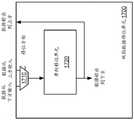
图5是根据实施例的显示系统500的高级框图。显示系统500包括光发射器(例如,uLED)的发射器阵列510。发射器阵列510可以是1D阵列(例如,每种颜色有1×N个发射器)或2D阵列(例如,每种颜色有N×M个发射器)。显示系统500还包括驱动电路512、数据移位电路520以及通信耦合到驱动电路512和数据移位电路520的显示驱动器530。5 is a high-level block diagram of a display system 500 according to an embodiment. Display system 500 includes an
驱动电路512包括一组电部件,其可操作以在显示驱动器530的控制下产生到发射器阵列510的输入。例如,驱动电路512可以包括提供控制信号的电压和/或电流发生器,该控制信号确定发射器阵列的光输出。驱动电路512可以包括用于发射器阵列510的每个发射器的单独电路。在一些实施例中,驱动电路512被组织为电子器件的有源矩阵,其中矩阵的布局与发射器阵列的布局镜像。驱动电路512可以位于发射器阵列510附近,并且可以通过一个或更多个通信总线连接到发射器阵列,该通信总线包括例如行和/或列选择线和用于向发射器阵列提供输入数据的线。驱动电路的示例构建块在下面描述,并且在本文被称为发射器单元。为了更好地解释驱动电路和发射器之间的相互作用,发射器单元在图中被示为包括发射器(被描绘为发光二极管)。然而,将理解,发射器可以远离发射器单元的其余部分定位。
数据移位电路包括多个存储元件(例如,图4A至图4E的存储元件414),用于存储数据和将数据移位到发射器阵列510中的发射器中。像驱动电路512一样,数据移位电路520可以与发射器阵列510物理分离,并且可以使用一条或更多条通信总线耦合到发射器阵列510。在一些实施例中,数据移位电路520被集成到驱动电路512或显示驱动器530中。例如,驱动电路512可以使用包括内置数据移位元件的发射器单元来形成。The data shift circuit includes a plurality of storage elements (eg,
显示驱动器530被配置成使用模拟和/或数字控制信号来控制驱动电路512向发射器提供图像数据。显示驱动器530还被配置为控制数据移位电路520的操作,特别是图像数据被加载到存储元件中和从存储元件移位出的定时(timing)。显示驱动器530可以与发射器的扫描同步地生成图像数据。例如,显示驱动器530可以控制数据被输入到列中的第一发射器的定时,以及数据被移位到该列中的剩余发射器的定时,其中该定时相对于由显示驱动器530控制的扫描镜的瞬时位置。具体地,显示驱动器530可以控制定时,使得来自同一列中的不同发射器的光输出被组合成输出图像的单个像素。
在一些实施例中,显示驱动器530通过连接到驱动电路512的反馈路径515通信耦合到发射器阵列。反馈路径515提供指示发射器阵列的操作状态或健康状况的信号传输。显示驱动器530可以处理该反馈信息,以调整发射器阵列510的操作,例如,通过增加其他发射器的输出来弥补有缺陷的发射器的缺失贡献,从而补偿有缺陷的发射器。在图20中示出了具有反馈能力的示例显示系统。In some embodiments,
图6是根据实施例的包括数据移位元件的显示系统600的简化框图。显示系统600包括显示驱动器610和多个发射器列615。特定颜色的每一列耦合到各自的数据移位寄存器。例如,第一列红色发射器耦合到数据移位寄存器620-A,以及第M列红色发射器耦合到数据移位寄存器620-M。类似地,分别为绿色和蓝色发射器提供数据移位器630和640。显示驱动器610被配置成生成使能信号652、多个扫描信号654和多个数据信号656。数据移位寄存器620、630和640中的每一个可以耦合到显示驱动器610的输出。使能信号652是使列能够被激活的全局信号。扫描信号654被顺序地生效(assert)以顺序地扫描代表每种颜色的图像数据的N行。数据信号656向多列提供图像数据,一次一行。6 is a simplified block diagram of a
如结合图4A至图4E所解释的,代替逐行编程发射器,可以通过在每行时间仅编程(针对每种颜色的)一行来增加数据吞吐量,因为数据可以被同一列中的其他发射器重用。因此,例如,数据移位寄存器620可以将图像数据从特定列的第一红色发射器移位到第N个红色发射器。类似地,数据移位寄存器630和640可以将数据从特定列的第一蓝色或绿色发射器移位到第N个蓝色或绿色发射器。As explained in conjunction with Figures 4A-4E, instead of programming the transmitter row by row, data throughput can be increased by programming only one row (for each color) at each row time, since data can be transmitted by other transmitters in the same column device reuse. Thus, for example,
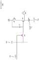
图7是根据实施例的可编程模拟发射器单元700的电路图。发射器单元700包括连接在晶体管M1和公共阴极715之间的发射器712。公共阴极715可以由相同颜色的发射器共享,包括不同列中的发射器,并且可以根据颜色设置为特定的电压电平。虽然简单的接地节点通常足以用于驱动发射器712,但是具有可控的公共阴极有助于使用移位的数据对发射器单元进行编程。发射器单元700还包括晶体管M2、M3和M4、以及存储电容器C1。M1、M2和M3可以是p沟道金属氧化物半导体场效应晶体管(p型MOSFET或PMOS)。M4可以是n型MOSFET或NMOS。FIG. 7 is a circuit diagram of a programmable
可以通过生效信号“行选择”720(例如,图6中的扫描信号654之一)来编程发射器单元700,该信号连接到M2的栅极。生效信号720导致数据信号730(例如,数据信号656之一)传递通过M2并作为电荷存储在电容器C1上,即C1被充电到代表数据信号730的电压。电容器C1连接在电源电压Vdd和M1的栅极之间。然后,电容器C1的电压可用于驱动M1,同时激活晶体管M3,从而建立从Vdd到M1的电流路径,产生与C1的电压成比例的通过M1(从而通过发射器712)的电流。通过M1的电流可以通过M4输出到另一个电路。图9中示出了支持数据移位的发射器单元700的变形。
图8是根据实施例的数字发射器单元800的电路图。发射器单元800包括三个PMOS晶体管M1、M2和M3以及一个发射器812。发射器812的阳极侧连接到晶体管M2和M3。发射器812也连接到公共阴极。M1连接在电源电压Vdd(例如+1V)和M2之间。M1的栅极由与(AND)逻辑门850的输出控制,与逻辑门850的输入是全局开/关信号和发射器开/关信号。M2的栅极连接到全局电流镜信号816,其可用于同时在多个发射器单元800的M2产生相同的驱动电流。因此,M1用作断开/闭合开关,M2设置驱动电流。M3处于二极管连接的配置中,并且接收偏置电压814(例如-1V)。M3操作来短路发射器812,以确保在发射器不应该发光的时候发射器被完全去激活(关闭)。图15中示出了支持数据移位的发射器单元800的变形。FIG. 8 is a circuit diagram of a
现在将描述用于在发射器单元之间移位数据的示例数据移位电路。本文描述的各种数据移位电路可以用于顺序地将数据移入和移出发射器单元,例如,用于实现先前关于图4A至图4E描述的移位过程。An example data shift circuit for shifting data between transmitter cells will now be described. The various data shifting circuits described herein can be used to sequentially shift data in and out of transmitter cells, eg, to implement the shifting processes previously described with respect to Figures 4A-4E.
模拟数据移位analog data shift
图9是根据实施例的包括数据移位部件的模拟发射器单元900的电路图。发射器单元900可以使用定时信号φ1和φ2以两个交替的阶段操作,并且包括电流镜块910和数据存储块920。发射器单元900包括八个晶体管M1至M8、两个存储电容器C1和C2以及发射器912(如前所述,发射器可以位于发射器单元的外部)。M1、M5、M6、M7和M8是NMOS。M2、M3和M4是PMOS,并且由于它们的源极节点连接到Vdd(基本恒定的电压),只要M2、M3和M4在饱和区工作,通过这些M2、M3和M4的电流仅取决于它们的栅极电压。在阶段1期间,φ1接通M1和M8以使输入电流“In”作为电压存储在电容器C1上。存储在C1上的电压是当作为栅极电压施加到M3上时足以再现输入电流的电压。M2在这段时间内也是导通的,以建立到Vdd的电流路径。在阶段1期间,公共阴极可以被设置为高,以确保发射器912被反向偏置,从而防止电流流过发射器912。反向偏置发射器提高了性能,尤其是对比度,因为更暗的“黑色”电平是通过防止漏电流效应实现的。反向偏置还将发射器与编程期间的闪烁噪声(flicker noise)隔离开来。在没有反向偏置的情况下,存储在C1上的电压可能在该编程阶段随时间变化,如果通过M3和发射器912的电流不恒定,则产生闪烁噪声。FIG. 9 is a circuit diagram of an
在阶段2期间,M1和M8断开,并且在阶段1期间存储在C1上的电压产生通过M3的驱动电流,以激活发射器912。在阶段2期间,公共阴极可以被设置为低,以便正向偏置发射器912(例如,通过将公共阴极接地),并允许驱动电流流过发射器912。此外,驱动电流被镜像到M4,因为M2、M3和M4的栅极被连接。镜像电流也被传递通过由φ2导通的M5和M6,作为电压存储在电容器C2上。在此期间,M7也导通,以建立到公共阴极的电流路径。由于M6开启,M7被置于二极管连接配置。因此,C2被充电到产生流经M5的电流所需的电压。如图10所示,连接M5、M6和M7的节点可以连接到发射器单元900的另一个实例的输入节点,以使得存储在C2上的电压能够在下一阶段1期间移位到另一个发射器单元。During
晶体管M2、M3、M4的尺寸可以被设定用于进行1对1电流镜像。可替代地,为了减少编程期间建立从Vdd到公共阴极的路径时引起的功耗,M3可以做得比M2和M4大。例如,如果相比于M2和M4,M3的宽度大十倍,那么C1可以用1/10的电流编程。Transistors M2, M3, M4 can be sized for 1-to-1 current mirroring. Alternatively, M3 can be made larger than M2 and M4 in order to reduce the power consumption caused by establishing the path from Vdd to the common cathode during programming. For example, if M3 is ten times wider than M2 and M4, then C1 can be programmed with 1/10 the current.
图10示出了在发射器单元900的两个实例之间的数据移位。该图的上半部分显示了在阶段1期间形成的电流路径。下半部分显示了在阶段2期间形成的电流路径。电流路径用粗线表示。在阶段1中,通过发射器单元900-A的M1、M2和M8形成电流路径。如前所述,这导致电压被存储在C1上。此外,在发射器单元900-B中同时发生相同的存储过程,其中发射器单元900-B的M1的数据输入由根据先前存储在发射器单元900-A的C2上的电压产生的电流提供。发射器单元900-A的M7被接通并充当电流吸收器(current sink),存储在C2上的电压形成M7的栅极电压。因此,发射器单元900-A的输出电流(以及发射器单元900-B的输入电流)与先前用于编程发射器单元900-A的C2的电流相同。以这种方式,先前用于驱动发射器单元900-A的数据被移位到发射器单元900-B中。FIG. 10 shows data shifting between two instances of
在阶段2中,根据在阶段1期间先前存储在发射器单元900-A的C1上的电压,使用通过M3的驱动电流来激活发射器单元900-A的发射器。如果存在通过公共阴极的电流路径(例如,如果公共阴极接地并且不保持浮动),则发射器将被激活。此外,通过将驱动电流镜像到发射器单元900-A的M4和M5,C1的电压被转移到发射器单元900-A的C2。在发射器单元900-B中同时发生相同的过程,其中根据存储在发射器单元900-B的C1上的电压(即,在阶段1期间从发射器单元900-A的C2转移的电压)来驱动发射器单元900-B的发射器。In
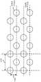
图11示出了用于实现一个或更多个实施例的具有幻像发射器(也称为虚拟(dummy)发射器)的发射器布局。该布局包括多行发射器,这些行发射器从上方和下方的相邻行偏移,使得发射器之间存在未被占据的空间。例如,一列中的发射器1112的中心到相邻列中的发射器1112的中心之间的水平距离1110可以比相邻行中的发射器中心之间的垂直距离1120长(例如,6微米对4.5微米)。这些未占用的空间对应于幻像发射器的位置。在一些实施例中,幻像发射器可以形成为保持未使用的物理发射器。虽然幻像发射器不产生光,但是当在发射器之间移位数据时,可以考虑到它们的存在。例如,如果数据要从发射器1112-A移位到发射器1112-B,则由于存在将发射器1112-A和1112-B分开的幻像发射器,所以数据可以在延迟一行时间后被移位。这种延迟的移位在前面结合图4A至图4E进行了描述。如现在将要解释的,可以使用被配置为临时存储幻像发射器的数据的数据存储电路来提供数据移位布置以适应幻像发射器的存在。这种数据存储电路在本文被称为幻像单元。11 illustrates a transmitter layout with phantom transmitters (also referred to as dummy transmitters) for implementing one or more embodiments. The layout includes rows of emitters that are offset from adjacent rows above and below such that there is unoccupied space between the emitters. For example, the
图12示出了根据实施例的模拟幻像单元1200。幻像单元1200与图9的发射器单元900相同,除了幻像单元1200不包括发射器,因此也不包括用于驱动发射器的晶体管M3。幻像单元1200可以以类似于发射器单元900的方式操作。特别地,在阶段1期间,φ1可以被生效以导通晶体管M1和M8,以使得输入电流“In”作为电压被存储到电容器C1上。然后,在阶段2期间,φ2可以被生效以导通晶体管M5和M6,同时将存储在C1上的电压作为栅极电压施加到M4上,从而使得相应的电压被存储在电容器C2上。幻像单元1200可以连接在两个发射器单元(例如,发射器单元900的两个实例,如图13所示)之间,使得幻像单元1200的电容器C2作为用于从一个发射器单元移位到另一个发射器单元的数据的临时储存器操作。FIG. 12 shows a
图13示出了电路1300,其包括连接在发射器单元900的两个实例之间的幻像单元1200。为了简单起见,省略了晶体管、电容器和发射器的标记。图13包括示出阶段1和阶段2的相对定时的示例时序图。如图所示,阶段1和阶段2是偏移的,在阶段1脉冲的结束和下一个阶段2脉冲的开始之间有轻微的延迟,反之亦然。FIG. 13 shows a
图14示出了包括连接在发射器单元1420-A和发射器单元1420-B之间的幻像单元1410的电路1400。像幻像单元1200一样,幻像单元1410可以用于在将数据从第一发射器单元(即,发射器1420-A)移位到第二发射器单元(即,发射器单元1420-B)时提供一行时间延迟。幻像单元1410包括类似的数据存储块,其中电容器C2和晶体管M5、M6和M7分别类似于幻像单元1200的C2、M5、M6和M7。然而,晶体管M1和M2使用第三定时信号φ3来控制,以实现第三阶段的操作。另外,幻像单元1410包括一对NMOS晶体管M10和M11。晶体管M10和M11在阶段1的交替部分(对应于定时信号φ1a和φ1b)被控制。Figure 14 shows a
发射器单元1420基本上与发射器单元900相同,除了省略了晶体管M1和M8。在阶段1的第一部分期间,φ1a被生效以激活M10,并将存储在发射器单元1420-A的C2上的电压传输到发射器单元1420-B的C1。在阶段2期间,φ2被生效以在每个发射器单元中将C1上的电压内部转换成C2上的相应电压,同时激活两个发射器。在阶段1的第二部分期间,φ1b被生效以激活M11,并将存储在幻像单元1410的C2上的电压传输到发射器单元1420-B的C1。在阶段3期间,φ3被生效以导通M5和M6,并将存储在发射器单元1420-A的C1上的电压传输到幻像单元1410的C2。Transmitter unit 1420 is substantially the same as
从图10、图13和图14的示例中,将理解,具有数据移位部件的模拟发射器单元可以连接在一起以形成一个链,并沿该链顺序地移位数据,其中可选的幻像单元放置在发射器单元之间。可以使用各种定时信号(例如φ1、φ2和公共阴极信号)来执行数据移位。这些定时信号可以由显示驱动器(诸如图5的显示驱动器530)产生。下面讨论具有数据移位部件的数字发射器单元和具有位于发射器单元外部的数据移位部件的电路的示例。From the examples of Figures 10, 13 and 14, it will be appreciated that analog transmitter units with data shifting components can be connected together to form a chain and sequentially shift data along the chain, with optional phantoms Units are placed between transmitter units. Data shifting can be performed using various timing signals such as φ1 , φ2 and a common cathode signal. These timing signals may be generated by a display driver, such as
数字数据移位digital data shift
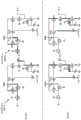
图15示出了数字发射器单元1500和数字幻像单元1550,二者都具有数据移位逻辑。发射器单元1500包括一对PMOS晶体管M1和M2以及连接在M2和公共阴极之间的发射器1510。发射器单元1500还包括数字移位寄存器1515,其包括多个1位移位级1512。每个移位级可以使用一组晶体管形成(例如,每级六个晶体管)。级数取决于要存储的值。例如,可以使用八个1位移位级来存储8位值。移位寄存器1515操作以基于时钟信号通过移位级1512一次将数据移位一位。晶体管M2由施加到M2的栅极的驱动信号控制。驱动信号确定流经M2的电流的大小,从而确定流经发射器1510的电流的大小。该驱动信号可以从电流源获得,并使用电流镜复制,以应用于发射器单元1500的附加实例。虽然通过发射器1510的电流大小由驱动信号确定,但是发射器1510的激活持续时间由时钟信号确定。如图15的底部所示,时钟信号可以被设置为不同持续时间的脉冲。脉冲持续时间对应于二进制编码的数据值(例如,从20到27)。因此,时钟信号可以用于通过脉宽调制来控制发射器1510的光输出。Figure 15 shows a digital transmitter unit 1500 and a
幻像单元1550包括数字移位寄存器1555,其包括与移位寄存器1515的移位级1512类似的1位移位级1552。通过将移位寄存器1515的输出连接到移位寄存器1555的输入,发射器单元1500可以耦合到幻像单元1550。类似地,在发射器单元1500的另一个实例中,如果不需要幻像单元,那么移位寄存器1515的输出可以连接到移位寄存器1515的输入。
图16示出了数字发射器单元1600和数字幻像单元1650。发射器单元1600和幻像单元1650是基于锁存的实现,与图15的实施例相反,它们不包括移位寄存器。发射器单元1600包括边沿触发锁存器1612,其接收时钟信号和数据信号作为输入。时钟信号和数据信号对应于图15中的时钟和数据信号,除了不是一次一位地顺序输入数据,而是同时锁存整个数据输入(例如,8位二进制值)。锁存器1612操作以临时存储数据输入,该数据输入然后基于从存储在锁存器1612中的数据中选择1位值的选择信号,由2对1多路复用器1614多路复用到PMOS晶体管1616的栅极上。选择信号可以是应用于发射器单元1600的其他实例的全局信号。幻像单元1650包括边沿触发锁存器1652,其接收与锁存器1612相同的时钟和数据输入信号。幻像单元1650不包括多路复用器,因为锁存器1652中存储的数据没有驱动发射器。FIG. 16 shows a digital transmitter unit 1600 and a digital phantom unit 1650. Transmitter unit 1600 and phantom unit 1650 are latch-based implementations that, contrary to the embodiment of FIG. 15, do not include shift registers. The transmitter unit 1600 includes an edge-triggered
附加数据移位实施例Additional Data Shift Example
图17是双向数据移位单元1700的简化框图。上述实施例提供了在一系列或一串发射器单元中数据从一个发射器单元到下一个发射器单元的单向移位。在某些情况下,可能希望允许双向数据移位。为了适应两个方向的移位,2对1多路复用器1710可以与单向移位单元1720(例如,包括数据移位能力的任何前述发射器或幻像单元)组合。可以控制多路复用器从上面(例如,前一个发射器单元)选择数据,或者从下面(例如,下一个发射器单元)选择数据,以便移入单向移位单元1720。移位方向由移位方向选择信号确定。单向移位单元1720的输出可以被提供给前一个发射器单元和下一个发射器单元,以便也为那些单元中的双向移位提供数据。FIG. 17 is a simplified block diagram of a bidirectional data shift unit 1700 . The above-described embodiments provide for unidirectional shifting of data from one transmitter unit to the next in a series or train of transmitter units. In some cases, it may be desirable to allow bidirectional data shifting. To accommodate shifting in both directions, the 2-to-1
图18是显示系统1800的简化框图,其是图5中显示系统500的实施例。显示系统1800是其中数据移位部件与发射器单元分开定位的系统的示例。显示系统1800包括数据移位电路1810、显示驱动器1820和发射器阵列1830。FIG. 18 is a simplified block diagram of
数据移位电路1810包括多个移位寄存器1812,每个移位寄存器被分配给发射器阵列1830中的发射器单元。例如,每个移位寄存器1812可以是例如使用如图15的实施例所示的八个1位级实现的8位移位寄存器。如图18所示,发射器阵列1830可以由模拟发射器单元(例如图7的发射器单元700)形成。然而,数据移位电路1810可以与任何类型的发射器单元(例如,图8的数字发射器单元)结合使用。为了说明的目的,发射器阵列1830被描绘为仅具有一行发射器单元。数据移位电路1810还包括多个移位寄存器1814,每个移位寄存器被分配给一个幻像单元。移位寄存器1812和1814以交替的方式连接。移位寄存器1812和1814中的每一个被配置为接收数据值(例如,8位值),该数据值被顺序移位通过移位寄存器的整个链。数据值可以由显示驱动器1820的处理器产生,其还包括用于驱动发射器阵列1830的电路。存储在移位寄存器1812中的值被提供给多路复用器1816,该多路复用器1816在图中被示为8对1、8位多路复用器,该多路复用器从八个移位寄存器1812之一中选择一个8位值以输出到显示驱动器1820。选择输出哪个移位寄存器值是基于选择信号(例如,包括单独的信号C0、C1和C2的3位信号),该选择信号可以由显示驱动器1820产生。
显示驱动器1820包括数模转换器(DAC)1822和用于驱动发射器阵列1830的输出缓冲器1824。DAC 1822操作来将从多路复用器1816输出的数字值转换成输入到输出缓冲器1824的模拟电压。输出缓冲器连接到整行发射器单元,从而通过生效行选择信号(例如,图7中的行选择信号),输出缓冲器1824产生的电流信号可以作为输入施加到发射器单元中的特定发射器单元。显示驱动器1820控制数据移位电路1810,使得多路复用器1816选择适当的移位寄存器1812,用于向该特定发射器单元提供输入。
使用电路1810的数据移位可以包括例如:Data shifting using
在时间段T1期间,将第一数据值存储到移位寄存器1812-A中,并通过多路复用器1816发送由移位寄存器1812-A输出的第一数据值以驱动行1发射器;During time period T1, the first data value is stored into shift register 1812-A, and the first data value output by shift register 1812-A is sent through
在时间段T2期间,将第一数据值从移位寄存器1812-A移位到移位寄存器1814-A中,将第二数据值存储到移位寄存器1812-A中,并且使用由移位寄存器1812-A输出的第二数据值来驱动行1发射器;During time period T2, the first data value is shifted from shift register 1812-A into shift register 1814-A, the second data value is stored into shift register 1812-A, and the The second data value output by the 1812-A to drive the row 1 transmitter;
在时间段T3期间,将第一数据值从移位寄存器1814-A移位到移位寄存器1812-B中,使用由移位寄存器1812-B输出的第一数据值驱动行2发射器,将第二数据值从移位寄存器1812-A移位到移位寄存器1814-A中,将第三数据值存储到移位寄存器1812-A中,并且使用由移位寄存器1812-A输出的第三数据值驱动行1发射器;以此类推。发射器阵列的每一列可以设置有其自己的数据移位电路1810的实例,以允许存储该列的发射器的数据。然而,一些部件可以由两列或更多列共享(例如,可以共享DAC 1822)。During time period T3, the first data value is shifted from shift register 1814-A into shift register 1812-B, the
图19是模拟数据移位电路1900的简化框图。类似于图18的数据移位电路1810,数据移位电路1900与发射器阵列的发射器单元分开定位。数据移位电路1900包括DAC 1910、解复用器1920、多路复用器1930、一组写门1922和一组读门1932。门1922和1932是传输门。DAC 1910被配置成接收数字输入数据(例如,来自显示驱动器的8位值),并将数字输入转换成输入到解复用器1920的模拟表示(例如,模拟电压)。19 is a simplified block diagram of an analog
解复用器1920被配置为基于选择信号(例如,C0、C1和C2)来向写门1922之一输出模拟电压。例如,解复用器1920可以是连接到八个写门1922的1对8解复用器,每个写门与特定的发射器行相关联。除了最后一个写门1922-N之外,每个写门1922可操作来将解复用器1920的输出连接到对应的1对2解复用器1942的输入。每个解复用器1942又在其输出端连接到2对1多路复用器1952。
连接在每个解复用器-多路复用器对1942、1952之间的是一对存储电容器,每个电容器可操作来存储由解复用器1942提供的模拟数据值。解复用器1942的选择输入确定该对存储电容器中的哪个电容器接收解复用器1942的输出。可以使用多路复用器1952读出存储在电容器上的值,多路复用器1952在其输出端连接到读门1932中的相应的读门。最后一个写门1922-N在其输出端直接连接到读门1932-N,其间仅连接一个存储电容器。对于八个发射器的列,总共可以使用15个数据电容器来临时存储用于移入发射器中的数据值,一个电容器用于八个发射器中的每一个,以及一个电容器用于连接在发射器之间的七个幻像发射器中的每个。Connected between each demultiplexer-
多路复用器1930被配置为读取存储在数据电容器上的电压,并(例如,基于用于解复用器1920的相同控制信号)选择存储的电压之一以输出到显示驱动器(未示出)。由于解复用器输出的电压是模拟的,因此不需要数模转换。替代地,显示驱动器可以简单地通过输出缓冲器缓冲模拟电压并将其缓冲到发射器阵列中的选定发射器中(例如,缓冲到发射器列中的特定行)。如同显示系统1800,发射器阵列的发射器单元可以是模拟发射器单元或数字发射器单元。Multiplexer 1930 is configured to read the voltages stored on the data capacitors and select one of the stored voltages (eg, based on the same control signal used for demultiplexer 1920) to output to a display driver (not shown). out). Since the voltage output by the demultiplexer is analog, no digital-to-analog conversion is required. Alternatively, the display driver may simply buffer the analog voltage through an output buffer and buffer it into a selected emitter in the emitter array (eg, into a particular row in a column of emitters). As with
此外,可以看出,与数据移位电路1810不同,数据移位电路1900内没有内部数据移位。替代地,数据只是简单地写入和读出适当的电容器。在任何给定时间,整列的数据可用于选择适当的模拟值来驱动相应的发射器。可以通过控制解复用器1920将电荷存储到选定的电容器上(例如,存储数据1),同时通过多路复用器1930将电荷从相同的选定电容器输出到选定的发射器来对数据移位电路1900编程。可以针对该列的剩余发射器重复该存储和驱动过程。Furthermore, it can be seen that, unlike
使用电路1900的数据移位可以包括例如:Data shifting using
在时间段T1期间,将数据1存储在第一电容器上,并使用数据1来驱动行1发射器;During time period T1, store data1 on the first capacitor and use data1 to drive the row 1 transmitter;
在时间段T2期间,将数据2存储在第二电容器上,使用数据1驱动行2发射器,并使用数据2驱动行1发射器(如果行2发射器是幻像发射器,则数据1可能不需要被读入多路复用器1930);During time period T2, data2 is stored on the second capacitor, data1 is used to drive the
在时间段T3期间,将数据3存储在第三电容器上,并使用数据1、数据2和数据3分别驱动行3、行2和行1发射器;以此类推。During time period T3, data3 is stored on the third capacitor, and data1 , data2 and data3 are used to drive the row 3,
在存储了最终数据值(例如,数据15)之后,可以存储新的数据1(覆盖第一电容器上的先前值),用于驱动同一列的行1发射器。与数据移位电路1810一样,发射器阵列的每一列可以被提供有其自己的数据移位电路1900的实例,但是一些部件(例如,DAC 1910)可以由两列或更多列共享。After the final data value (eg, data15 ) is stored, a new data1 (overwriting the previous value on the first capacitor) can be stored for driving the row 1 transmitter of the same column. As with
反馈电路feedback circuit
图20是具有反馈收集能力的显示系统2000的简化框图。系统2000包括显示驱动器2010和驱动电路2020。驱动电路2020可以使用先前描述的模拟或数字发射器单元中的任何一个来形成,并且如图所示,具有以阵列形式排列的一组发射器单元2012(例如,以与由发射器单元2012驱动的物理发射器相同的行和列配置排列)。由发射器单元2012驱动的发射器连接到公共阴极2015。为简单起见,仅示出了一个发射器2014。显示系统2000包括数据移位部件(未示出),如结合上述实施例所描述的,这些数据移位部件可以集成到发射器单元中或者单独位于显示系统的另一个区域中。如前所述,发射器单元可以连接成链以形成一列,使得数据从第一行的发射器单元顺序移位到最后一行的发射器单元。因此,基于由显示驱动器2010提供的用于驱动列2017的发射器的数字数据值(或其模拟表示),发射器2014可以对应于要被驱动的最后的发射器。列包括用于驱动相同颜色的发射器的发射器单元。存在用于驱动其他颜色发射器的附加列,但是从图中省略了这些附加列。20 is a simplified block diagram of a
显示驱动器2010被配置成独立地控制一对开关2025和2027,开关2025和2027可连接到列2017(例如,M个列的列1)的最后一个发射器单元2012-N。更具体地,开关2025和2027分别可连接到发射器2014的阳极和阴极2015。阴极2015可以是所有列共享的公共阴极。开关2025和2027可以实现为晶体管(例如,一对NMOS晶体管)。可以为每个剩余的列提供一对类似的开关,以便能够测试这些列。还描绘了连接在发射器2014和公共阴极2015之间的虚拟(fictitious)电流源2022。电流源2022表示偏置电流,该偏置电流是由于在整个列2017中移位测试值而产生的。因此,电流源2022基于输入到列的测试值是可控的。显示驱动器2010可以选择测试值为任何非零数据值,对于该值,反馈处理单元2019可以获得期望的反馈特性。Display driver 2010 is configured to independently control a pair of
为了执行反馈分析,显示驱动器2010可以将公共阴极2015设置为浮动电压,同时保持开关2025断开而开关2027闭合。在这种配置中,来自电流源2022的电流将流过发射器2014并进入反馈路径2050。此外,如果对剩余列的数据输入被设置为零(即,如果被移位的唯一数据是测试值,并且仅通过列2017),则通过反馈路径2050的电流将指示发射器2014是否通过以与测试值成正确的比例的电流。To perform the feedback analysis, the display driver 2010 can set the
反馈处理单元2019可以用硬件、软件或其组合来实现。反馈处理单元2019可以被配置为将反馈路径2050中的电流与同测试值相关联的预期电流进行比较。该预期电流例如可以是在列2017正常工作时测量的存储参考电流,即历史电流。可替代地,预期电流可以是基于驱动电路2020的设计规范确定的存储值。The feedback processing unit 2019 may be implemented in hardware, software, or a combination thereof. The feedback processing unit 2019 may be configured to compare the current in the feedback path 2050 with the expected current associated with the test value. The expected current may be, for example, a stored reference current measured when the
作为另一种类型的反馈分析,显示驱动器2010可以向公共阴极2015施加电压偏置,同时保持开关2025闭合和开关2027断开。在这种配置中,反馈路径2050可以用于测量跨发射器2014产生的电压。因此,反馈路径2050可以基于开关2025和2027的断开/闭合配置来定义,这取决于感兴趣哪个电特性。类似于用于测量反馈电流的配置,可以存储预期电压,用于由反馈处理单元2019与测量的电压进行比较。As another type of feedback analysis, display driver 2010 may apply a voltage bias to
反馈处理单元2019可以分析反馈以确定列2017的整体健康状况。因为列2017的发射器单元2012都是连接的,所以列中的每个发射器单元都对测量的电流或测量的电压有贡献,这因此指示了整个列的性能。反馈处理单元2019可以基于测量的电流/电压值不同于预期的电流/电压来确定列2017中的某处存在问题。与预期电流/电压的偏差可由例如制造缺陷、具有相同设计规格的部件之间的固有差异或由部件老化引起的性能退化导致。偏差的源可以是列2017的发射器单元中的任何部件,包括例如产生由电流源2022表示的电流所涉及的晶体管、存储电容器或发射器。因为测量的信号不特定于任何单个发射器单元,所以反馈处理单元2019不能确定问题的确切位置。然而,显示驱动器2010可以被调整以校正该问题,例如,如果测量的电流小于预期电流,则增加列2017的后续输入的数据值。例如,反馈处理单元2019可以通过基于测量的电流低于预期电流的量确定该列中的两个发射器单元有缺陷(例如,基于当每个发射器单元完全起作用时每个发射器单元对测量的电流或电压的贡献相等的假设)来计算该增加。显示驱动器2010然后可以通过将数据输入增加与电流差除以该列中无缺陷发射器单元的总数相对应的量来补偿电流差。Feedback processing unit 2019 may analyze the feedback to determine the overall health of
反馈分析可用于补偿制造缺陷和构成驱动电路2020的各种电部件的设备公差中的差异。反馈分析也可以在显示系统2000的整个寿命期间偶尔执行。例如,显示驱动器2010可以被配置成以规则的间隔自动执行反馈分析,以便监控驱动电路2020的健康状况。可以在扫描显示器以产生供用户观看的输出图像时收集反馈。也可以在不产生输出图像的情况下收集反馈(例如,在扫描组件保持静止的同时将测试值移位通过一列或更多列)。因此,由于驱动电路2020中的部件老化(包括物理发射器的老化)导致的性能退化可以被及时检测和补偿。Feedback analysis can be used to compensate for manufacturing defects and differences in device tolerances of the various electrical components that make up the driver circuit 2020 . Feedback analysis may also be performed occasionally throughout the life of the
在一些实施例中,一列中有多对开关。例如,每个发射器可以连接到相应的一对开关,每对开关连接到单独的反馈路径,以实现特定于驱动该特定发射器的发射器单元的测量。然而,当聚集发射器单元的贡献时,例如,根据先前描述的实施例,通过在整个列中移位数据,通常不需要获得关于哪个特定发射器单元有问题的精确信息。In some embodiments, there are multiple pairs of switches in a column. For example, each transmitter may be connected to a corresponding pair of switches, each pair of switches being connected to a separate feedback path to enable measurements specific to the transmitter unit driving that particular transmitter. However, when aggregating the contributions of transmitter cells, eg, by shifting the data throughout the column, according to the previously described embodiments, it is generally not necessary to obtain precise information about which particular transmitter cell is in question.
图21是用于校准驱动电路的方法2100的流程图。方法2100可以使用显示系统2000来执行。在步骤2110,数据值被移位通过发射器单元的单行或列。数据值可以是任何非零值。显示驱动器2010可以从存储在存储器中的一组历史或编程数据值中选择数据值。例如,数据值可以存储在将数据值映射到预期电流或电压的表中。当数据值被移位时,剩余的行或列被设置为零。21 is a flowchart of a
在步骤2120,显示驱动器2010配置从数据值在步骤2110中移位通过其的行/列的最后一个发射器开始的反馈路径。显示驱动器2010可以通过选择性地断开或闭合可连接到最后一个发射器的一对开关来配置反馈路径。如以上结合图20所解释的,开关的断开/闭合配置可用于执行特定类型的测量(例如,电流测量或电压测量)。At
在步骤2130,显示驱动器2010的反馈处理单元测量通过反馈路径接收的信号。测量过程可以包括存储测量信号的表示(例如,使用模数转换器将测量电流转换成数字值,或者将测量电流存储为电容器上的电压)。At
在步骤2140,反馈处理单元将测量信号的值与期望值进行比较。该比较可以包括执行一个或更多个计算(例如,从另一个值中减去一个值以确定两个值之间的差)。在一些实施例中,使用通用处理器(例如,计算机的中央处理单元)来执行比较。在其他实施例中,使用专用电路(例如,模拟比较器)来执行比较。At
在步骤2150,根据两个值之间的差来调整显示驱动器2010的未来数据输出。例如,如前所述,随后移位到同一行/列的数据的值可以增加一定量,该量基于测量值和期望值之间的差来计算,并且进一步基于当行/列的所有发射器单元都完全起作用时发射器单元对测量电流或电压的贡献相等的假设。反馈处理单元可以基于两个值之间的差来确定有多少发射器单元有缺陷,并且可以基于无缺陷的发射器单元的数量来设置增加量。例如,如果测量电流比期望电流小200微安,并且有五个无缺陷的发射器单元,则行/列的后续输入可以增加导致额外施加40微安的数据值。由于数据值移位通过行/列中的每个发射器单元,因此产生的总附加电流将为5×40微安或200微安。如果需要,可以类似地减小数据值。At
出于说明的目的,已经呈现了本公开的实施例的前述描述;它并不旨在穷举或将本公开限制于所公开的精确形式。相关领域的技术人员可以理解,根据上述公开,许多修改和变化是可能的。The foregoing description of the embodiments of the present disclosure has been presented for purposes of illustration; it is not intended to be exhaustive or to limit the disclosure to the precise forms disclosed. Those skilled in the relevant art will appreciate that many modifications and variations are possible in light of the above disclosure.
本说明书的一些部分根据信息操作的算法和符号表示来描述本公开的实施例。这些算法描述和表示通常被数据处理领域的技术人员用来将他们工作的实质有效地传达给本领域的其他技术人员。这些操作虽然在功能上、计算上或逻辑上被描述,但被理解为由计算机程序或等效电路、微码等来实现。此外,在不失一般性的情况下,将这些操作安排称为模块有时也被证明是方便的。所描述的操作及其相关模块可以用软件、固件和/或硬件来实现。Portions of this specification describe embodiments of the present disclosure in terms of algorithms and symbolic representations of information operations. These algorithmic descriptions and representations are commonly used by those skilled in the data processing arts to effectively convey the substance of their work to others skilled in the art. These operations, although described functionally, computationally, or logically, are understood to be implemented by a computer program or equivalent circuit, microcode, or the like. Furthermore, it has also proven convenient at times, without loss of generality, to refer to these arrangements of operations as modules. The described operations and their associated modules may be implemented in software, firmware and/or hardware.
所描述的步骤、操作或过程可以用一个或更多个硬件或软件模块单独或与其他设备结合来执行或实现。尽管步骤、操作或过程是按顺序描述的,但是将理解,在一些实施例中,顺序次序可以不同于已经描述的顺序,例如,某些步骤、操作或过程被省略或并行或并发执行。在一些实施例中,软件模块用计算机程序产品来实现,该计算机程序产品包括包含计算机程序代码的计算机可读介质,该计算机程序代码可以由一个或更多个计算机处理器来执行,用于执行所描述的任何或所有步骤、操作或过程。The steps, operations or processes described may be performed or implemented using one or more hardware or software modules alone or in combination with other devices. Although steps, operations or processes are described sequentially, it will be understood that in some embodiments the sequential order may differ from the order that has been described, eg, certain steps, operations or processes are omitted or performed in parallel or concurrently. In some embodiments, software modules are implemented in a computer program product comprising a computer-readable medium containing computer program code executable by one or more computer processors for performing any or all of the steps, operations or processes described.
本公开的实施例还可以涉及用于执行所描述的操作的装置。该装置可以为所需目的而专门构造,和/或它可以包括由存储在计算机中的计算机程序选择性激活或重新配置的通用计算设备。这样的计算机程序可以存储在非暂时性的、有形的计算机可读存储介质中,或者任何类型的适于存储电子指令的介质中,其可以耦合到计算机系统总线。此外,本说明书中提到的任何计算系统可以包括单个处理器,或者可以是采用多处理器设计以提高计算能力的体系结构。Embodiments of the present disclosure may also relate to apparatuses for performing the described operations. This apparatus may be specially constructed for the required purposes, and/or it may comprise a general-purpose computing device selectively activated or reconfigured by a computer program stored in the computer. Such a computer program may be stored in a non-transitory, tangible computer-readable storage medium, or any type of medium suitable for storage of electronic instructions, which may be coupled to a computer system bus. Furthermore, any computing system mentioned in this specification may include a single processor, or may be an architecture that employs a multi-processor design to increase computing power.
说明书中使用的语言主要是出于可读性和指导性的目的而选择的,它可能不是为了描绘或限制本发明的主题而选择的。因此,意图是本公开的范围不被该详细描述所限制,而是被基于此的申请发布的任何权利要求所限制。因此,实施例的公开旨在说明而非限制本公开的范围,本公开的范围在所附权利要求中阐述。The language used in the specification has been principally selected for readability and instructional purposes and may not have been selected to delineate or limit the subject matter of the invention. It is, therefore, intended that the scope of the present disclosure be limited not by this detailed description, but by any claims that issue applications based thereon. Accordingly, the disclosure of the embodiments is intended to illustrate, but not to limit, the scope of the disclosure, which is set forth in the appended claims.
Claims (20)
Applications Claiming Priority (5)
| Application Number | Priority Date | Filing Date | Title |
|---|---|---|---|
| GR20170100527 | 2017-11-23 | ||
| GR20170100527 | 2017-11-23 | ||
| GR20180100411 | 2018-09-07 | ||
| GR20180100411 | 2018-09-07 | ||
| PCT/US2018/058804WO2019103821A1 (en) | 2017-11-23 | 2018-11-01 | Data shifting circuit for a current mode display |
Publications (1)
| Publication Number | Publication Date |
|---|---|
| CN111527538Atrue CN111527538A (en) | 2020-08-11 |
Family
ID=66533239
Family Applications (1)
| Application Number | Title | Priority Date | Filing Date |
|---|---|---|---|
| CN201880084774.3APendingCN111527538A (en) | 2017-11-23 | 2018-11-01 | Data Shift Circuits for Current Mode Displays |
Country Status (3)
| Country | Link |
|---|---|
| US (3) | US10930188B2 (en) |
| CN (1) | CN111527538A (en) |
| WO (1) | WO2019103821A1 (en) |
Cited By (2)
| Publication number | Priority date | Publication date | Assignee | Title |
|---|---|---|---|---|
| US10971061B2 (en) | 2019-01-11 | 2021-04-06 | Facebook Technologies, Llc | Control scheme for a scanning display |
| US11151916B2 (en) | 2017-11-23 | 2021-10-19 | Facebook Technologies, Llc | Data shifting circuit for a current mode display |
Families Citing this family (7)
| Publication number | Priority date | Publication date | Assignee | Title |
|---|---|---|---|---|
| CN108874150B (en)* | 2018-07-27 | 2024-08-20 | 华南理工大学 | Virtual reality tactile feedback interaction system |
| CA3109903C (en)* | 2018-10-01 | 2022-08-30 | Leia Inc. | Multiview display and method with offset rows of multibeam emitters and multiview pixels |
| US10804333B2 (en)* | 2018-11-16 | 2020-10-13 | Osram Opto Semiconductors Gmbh | Display, circuit arrangement for a display and method of operating a display |
| TWI707328B (en)* | 2019-09-17 | 2020-10-11 | 友達光電股份有限公司 | Driving chip and display device having the same |
| US11099393B2 (en)* | 2019-11-22 | 2021-08-24 | Facebook Technologies, Llc | Surface emitting light source with lateral variant refractive index profile |
| US11749964B2 (en) | 2020-06-24 | 2023-09-05 | Meta Platforms Technologies, Llc | Monolithic light source with integrated optics based on nonlinear frequency conversion |
| TWI761087B (en)* | 2021-02-23 | 2022-04-11 | 友達光電股份有限公司 | Driving circuit |
Citations (13)
| Publication number | Priority date | Publication date | Assignee | Title |
|---|---|---|---|---|
| US6268841B1 (en)* | 1998-01-09 | 2001-07-31 | Sharp Kabushiki Kaisha | Data line driver for a matrix display and a matrix display |
| US20030151569A1 (en)* | 2002-02-12 | 2003-08-14 | Eastman Kodak Company | Flat-panel light emitting pixel with luminance feedback |
| US6771232B2 (en)* | 2000-12-12 | 2004-08-03 | Nec Corporation | Mobile terminal device, content distribution system, content distribution method, and program for executing method thereof |
| US20040251973A1 (en)* | 2003-05-30 | 2004-12-16 | Masaaki Ishida | Voltage controlled oscillator, PLL circuit, pulse modulation signal generating circuit, semiconductor laser modulation device and image forming apparatus |
| US20070080905A1 (en)* | 2003-05-07 | 2007-04-12 | Toshiba Matsushita Display Technology Co., Ltd. | El display and its driving method |
| CN1967648A (en)* | 2005-11-17 | 2007-05-23 | 统宝光电股份有限公司 | Image display system and related method for providing driving voltage |
| US20100124438A1 (en)* | 2008-11-14 | 2010-05-20 | Akira Nagumo | Light emitting element array, drive circuit, optical print head, and image forming apparatus |
| US20110043541A1 (en)* | 2009-08-20 | 2011-02-24 | Cok Ronald S | Fault detection in electroluminescent displays |
| CN104115564A (en)* | 2011-12-08 | 2014-10-22 | 先进模拟科技公司 | Serial lighting interface with embedded feedback |
| US20150186098A1 (en)* | 2013-12-31 | 2015-07-02 | Ultravision Technologies, Llc | Modular Display Panels with Different Pitches |
| US20170214907A1 (en)* | 2012-08-04 | 2017-07-27 | Paul Lapstun | Head-Mounted Light Field Display |
| US20170236463A1 (en)* | 2016-02-11 | 2017-08-17 | Oculus Vr, Llc | Scanned microled array for waveguide display |
| CN110459174A (en)* | 2018-05-08 | 2019-11-15 | 苹果公司 | memory-in-pixel display |
Family Cites Families (25)
| Publication number | Priority date | Publication date | Assignee | Title |
|---|---|---|---|---|
| JPS5910073A (en)* | 1982-07-09 | 1984-01-19 | Canon Inc | recording device |
| US4855760A (en)* | 1987-03-12 | 1989-08-08 | Fuji Photo Film Co., Ltd. | LED array with graduated quantity control |
| US5331333A (en) | 1988-12-08 | 1994-07-19 | Sharp Kabushiki Kaisha | Display apparatus |
| US10593092B2 (en) | 1990-12-07 | 2020-03-17 | Dennis J Solomon | Integrated 3D-D2 visual effects display |
| US5612728A (en)* | 1994-05-20 | 1997-03-18 | Westinghouse Electric Corporation | Full color TFEL edge emitter printing system |
| US5710506A (en)* | 1995-02-07 | 1998-01-20 | Benchmarq Microelectronics, Inc. | Lead acid charger |
| US8282221B2 (en) | 2003-11-01 | 2012-10-09 | Silicon Quest Kabushiki Kaisha | Projection apparatus using variable light source |
| JP5449641B2 (en)* | 2006-04-17 | 2014-03-19 | グローバル・オーエルイーディー・テクノロジー・リミテッド・ライアビリティ・カンパニー | Display device |
| US7355574B1 (en)* | 2007-01-24 | 2008-04-08 | Eastman Kodak Company | OLED display with aging and efficiency compensation |
| US20090040198A1 (en) | 2007-08-09 | 2009-02-12 | Silicon Touch Technology Inc. | Method for detecting pixel status of flat panel display and display driver thereof |
| JP4682231B2 (en) | 2008-08-01 | 2011-05-11 | 株式会社沖データ | Optical print head and image forming apparatus |
| KR101065418B1 (en) | 2010-02-19 | 2011-09-16 | 삼성모바일디스플레이주식회사 | Display device and driving method thereof |
| JP4988893B2 (en)* | 2010-03-26 | 2012-08-01 | 株式会社沖データ | Drive circuit, drive device, and image forming apparatus |
| JP5687880B2 (en) | 2010-11-08 | 2015-03-25 | 船井電機株式会社 | Image display device |
| EP2610846A3 (en) | 2011-12-28 | 2014-07-09 | Samsung Electronics Co., Ltd. | Device and method for displaying image, device and method for supplying power, and method for adjusting brightness of contents |
| CN105900166B (en) | 2014-01-07 | 2019-03-01 | 三菱电机株式会社 | Image projection device and method of adjustment |
| CN105321445B (en) | 2014-05-30 | 2018-05-15 | 深圳市光峰光电技术有限公司 | Display control program and display device |
| JP6520209B2 (en) | 2015-02-27 | 2019-05-29 | セイコーエプソン株式会社 | Image display device |
| JP6966942B2 (en) | 2015-06-05 | 2021-11-17 | アップル インコーポレイテッドApple Inc. | Light emission control device and method for display panel |
| US10859834B2 (en)* | 2017-07-03 | 2020-12-08 | Holovisions | Space-efficient optical structures for wide field-of-view augmented reality (AR) eyewear |
| US10303044B2 (en) | 2017-09-26 | 2019-05-28 | Microvision, Inc. | Scanning mirror control and slow scan position offset |
| US10930188B2 (en) | 2017-11-23 | 2021-02-23 | Facebook Technologies, Llc | Feedback circuit for calibrating a current mode display |
| US10861380B2 (en) | 2018-05-14 | 2020-12-08 | Facebook Technologies, Llc | Display systems with hybrid emitter circuits |
| US11004372B2 (en) | 2018-12-11 | 2021-05-11 | Microsoft Technology Licensing, Llc | Controlling a scanning mirror system |
| US10971061B2 (en) | 2019-01-11 | 2021-04-06 | Facebook Technologies, Llc | Control scheme for a scanning display |
- 2018
- 2018-11-01USUS16/178,510patent/US10930188B2/enactiveActive
- 2018-11-01WOPCT/US2018/058804patent/WO2019103821A1/ennot_activeCeased
- 2018-11-01CNCN201880084774.3Apatent/CN111527538A/enactivePending
- 2018-11-01USUS16/178,505patent/US10937348B2/enactiveActive
- 2018-11-01USUS16/761,767patent/US11151916B2/enactiveActive
Patent Citations (15)
| Publication number | Priority date | Publication date | Assignee | Title |
|---|---|---|---|---|
| US6268841B1 (en)* | 1998-01-09 | 2001-07-31 | Sharp Kabushiki Kaisha | Data line driver for a matrix display and a matrix display |
| US6771232B2 (en)* | 2000-12-12 | 2004-08-03 | Nec Corporation | Mobile terminal device, content distribution system, content distribution method, and program for executing method thereof |
| US20030151569A1 (en)* | 2002-02-12 | 2003-08-14 | Eastman Kodak Company | Flat-panel light emitting pixel with luminance feedback |
| US20070080905A1 (en)* | 2003-05-07 | 2007-04-12 | Toshiba Matsushita Display Technology Co., Ltd. | El display and its driving method |
| US20040251973A1 (en)* | 2003-05-30 | 2004-12-16 | Masaaki Ishida | Voltage controlled oscillator, PLL circuit, pulse modulation signal generating circuit, semiconductor laser modulation device and image forming apparatus |
| CN1967648A (en)* | 2005-11-17 | 2007-05-23 | 统宝光电股份有限公司 | Image display system and related method for providing driving voltage |
| US20100124438A1 (en)* | 2008-11-14 | 2010-05-20 | Akira Nagumo | Light emitting element array, drive circuit, optical print head, and image forming apparatus |
| US20110043541A1 (en)* | 2009-08-20 | 2011-02-24 | Cok Ronald S | Fault detection in electroluminescent displays |
| CN104115564A (en)* | 2011-12-08 | 2014-10-22 | 先进模拟科技公司 | Serial lighting interface with embedded feedback |
| US20160198533A1 (en)* | 2011-12-08 | 2016-07-07 | Advanced Analogic Technologies Incorporated | Serial lighting interface with embedded feedback |
| US20170214907A1 (en)* | 2012-08-04 | 2017-07-27 | Paul Lapstun | Head-Mounted Light Field Display |
| US20150186098A1 (en)* | 2013-12-31 | 2015-07-02 | Ultravision Technologies, Llc | Modular Display Panels with Different Pitches |
| US20170236463A1 (en)* | 2016-02-11 | 2017-08-17 | Oculus Vr, Llc | Scanned microled array for waveguide display |
| US20170235143A1 (en)* | 2016-02-11 | 2017-08-17 | Oculus Vr, Llc | Waveguide display with two-dimensional scanner |
| CN110459174A (en)* | 2018-05-08 | 2019-11-15 | 苹果公司 | memory-in-pixel display |
Cited By (4)
| Publication number | Priority date | Publication date | Assignee | Title |
|---|---|---|---|---|
| US11151916B2 (en) | 2017-11-23 | 2021-10-19 | Facebook Technologies, Llc | Data shifting circuit for a current mode display |
| US10971061B2 (en) | 2019-01-11 | 2021-04-06 | Facebook Technologies, Llc | Control scheme for a scanning display |
| US11430384B2 (en) | 2019-01-11 | 2022-08-30 | Meta Platforms Technologies, Llc | Control scheme for a scanning display |
| US11798471B2 (en) | 2019-01-11 | 2023-10-24 | Meta Platforms Technologies, Llc | Control scheme for a scanning display |
Also Published As
| Publication number | Publication date |
|---|---|
| US10930188B2 (en) | 2021-02-23 |
| US20190156720A1 (en) | 2019-05-23 |
| US20200372846A1 (en) | 2020-11-26 |
| US10937348B2 (en) | 2021-03-02 |
| US11151916B2 (en) | 2021-10-19 |
| US20190156721A1 (en) | 2019-05-23 |
| WO2019103821A1 (en) | 2019-05-31 |
Similar Documents
| Publication | Publication Date | Title |
|---|---|---|
| US11151916B2 (en) | Data shifting circuit for a current mode display | |
| TWI778098B (en) | Light emitter architecture for scanning display device | |
| US10861380B2 (en) | Display systems with hybrid emitter circuits | |
| JP6791840B2 (en) | light source | |
| US20210225268A1 (en) | Display driver ic (ddic) backplane for scanning microled array | |
| US6736512B2 (en) | Pixel element for a three-dimensional screen | |
| US5903323A (en) | Full color sequential image projection system incorporating time modulated illumination | |
| JP4299790B2 (en) | Method and system for generating color using a low resolution spatial color modulator and a high resolution modulator | |
| EP3064994B1 (en) | System and method for increased spatial resolution | |
| KR20210121210A (en) | Pulse width modulation to drive pixels using a comparator | |
| US20060115923A1 (en) | Micromirror-based projection system and a method of making the same | |
| US20060066540A1 (en) | Spatial light modulation display system | |
| CN104541321A (en) | Display, display control method, display control device, and electronic apparatus | |
| US20040085271A1 (en) | Display system with display element storage | |
| US11798471B2 (en) | Control scheme for a scanning display | |
| CN102016695A (en) | Color display system | |
| Beasley et al. | Dynamic infrared scene projectors based upon the DMD | |
| CN110636226A (en) | Infrared dynamic scene driving control system and method | |
| EP4124209A1 (en) | Display driver ic (ddic) backplane for scanning microled array | |
| US8432341B2 (en) | Color sequence control for video display apparatus | |
| US8184133B2 (en) | Methods for sequential color display by modulation of pulses | |
| Nabha | 100 hz 512x512 sleds system design | |
| CN103809364A (en) | True three-dimensional image display system and true three-dimensional image display method | |
| Beasley et al. | Advancements in the micromirror array projector technology | |
| Dupuis et al. | Two-band DMD-based infrared scene simulator |
Legal Events
| Date | Code | Title | Description |
|---|---|---|---|
| PB01 | Publication | ||
| PB01 | Publication | ||
| SE01 | Entry into force of request for substantive examination | ||
| SE01 | Entry into force of request for substantive examination | ||
| CB02 | Change of applicant information | Address after:California, USA Applicant after:Yuan Platform Technology Co.,Ltd. Address before:California, USA Applicant before:Facebook Technologies, LLC | |
| CB02 | Change of applicant information | ||
| WD01 | Invention patent application deemed withdrawn after publication | Application publication date:20200811 | |
| WD01 | Invention patent application deemed withdrawn after publication |