CN111527536A - Display device and related integrated circuit, method and user equipment thereof - Google Patents
Display device and related integrated circuit, method and user equipment thereofDownload PDFInfo
- Publication number
- CN111527536A CN111527536ACN201780095864.8ACN201780095864ACN111527536ACN 111527536 ACN111527536 ACN 111527536ACN 201780095864 ACN201780095864 ACN 201780095864ACN 111527536 ACN111527536 ACN 111527536A
- Authority
- CN
- China
- Prior art keywords
- dic
- display screen
- fpc
- electrical connector
- bonding step
- Prior art date
- Legal status (The legal status is an assumption and is not a legal conclusion. Google has not performed a legal analysis and makes no representation as to the accuracy of the status listed.)
- Pending
Links
Images


Classifications
- G—PHYSICS
- G06—COMPUTING OR CALCULATING; COUNTING
- G06F—ELECTRIC DIGITAL DATA PROCESSING
- G06F1/00—Details not covered by groups G06F3/00 - G06F13/00 and G06F21/00
- G06F1/16—Constructional details or arrangements
- G06F1/18—Packaging or power distribution
- G06F1/189—Power distribution
- G—PHYSICS
- G09—EDUCATION; CRYPTOGRAPHY; DISPLAY; ADVERTISING; SEALS
- G09G—ARRANGEMENTS OR CIRCUITS FOR CONTROL OF INDICATING DEVICES USING STATIC MEANS TO PRESENT VARIABLE INFORMATION
- G09G3/00—Control arrangements or circuits, of interest only in connection with visual indicators other than cathode-ray tubes
- G09G3/20—Control arrangements or circuits, of interest only in connection with visual indicators other than cathode-ray tubes for presentation of an assembly of a number of characters, e.g. a page, by composing the assembly by combination of individual elements arranged in a matrix no fixed position being assigned to or needed to be assigned to the individual characters or partial characters
- G—PHYSICS
- G06—COMPUTING OR CALCULATING; COUNTING
- G06F—ELECTRIC DIGITAL DATA PROCESSING
- G06F1/00—Details not covered by groups G06F3/00 - G06F13/00 and G06F21/00
- G06F1/16—Constructional details or arrangements
- G06F1/18—Packaging or power distribution
- G06F1/181—Enclosures
- G—PHYSICS
- G09—EDUCATION; CRYPTOGRAPHY; DISPLAY; ADVERTISING; SEALS
- G09G—ARRANGEMENTS OR CIRCUITS FOR CONTROL OF INDICATING DEVICES USING STATIC MEANS TO PRESENT VARIABLE INFORMATION
- G09G2300/00—Aspects of the constitution of display devices
- G09G2300/04—Structural and physical details of display devices
- G09G2300/0404—Matrix technologies
- G09G2300/0408—Integration of the drivers onto the display substrate
- G—PHYSICS
- G09—EDUCATION; CRYPTOGRAPHY; DISPLAY; ADVERTISING; SEALS
- G09G—ARRANGEMENTS OR CIRCUITS FOR CONTROL OF INDICATING DEVICES USING STATIC MEANS TO PRESENT VARIABLE INFORMATION
- G09G2300/00—Aspects of the constitution of display devices
- G09G2300/04—Structural and physical details of display devices
- G09G2300/0421—Structural details of the set of electrodes
- G09G2300/0426—Layout of electrodes and connections
- G—PHYSICS
- G09—EDUCATION; CRYPTOGRAPHY; DISPLAY; ADVERTISING; SEALS
- G09G—ARRANGEMENTS OR CIRCUITS FOR CONTROL OF INDICATING DEVICES USING STATIC MEANS TO PRESENT VARIABLE INFORMATION
- G09G2310/00—Command of the display device
- G09G2310/02—Addressing, scanning or driving the display screen or processing steps related thereto
- G09G2310/0264—Details of driving circuits
- G09G2310/0281—Arrangement of scan or data electrode driver circuits at the periphery of a panel not inherent to a split matrix structure
- H—ELECTRICITY
- H01—ELECTRIC ELEMENTS
- H01L—SEMICONDUCTOR DEVICES NOT COVERED BY CLASS H10
- H01L2224/00—Indexing scheme for arrangements for connecting or disconnecting semiconductor or solid-state bodies and methods related thereto as covered by H01L24/00
- H01L2224/01—Means for bonding being attached to, or being formed on, the surface to be connected, e.g. chip-to-package, die-attach, "first-level" interconnects; Manufacturing methods related thereto
- H01L2224/02—Bonding areas; Manufacturing methods related thereto
- H01L2224/04—Structure, shape, material or disposition of the bonding areas prior to the connecting process
- H01L2224/06—Structure, shape, material or disposition of the bonding areas prior to the connecting process of a plurality of bonding areas
- H01L2224/061—Disposition
- H01L2224/0618—Disposition being disposed on at least two different sides of the body, e.g. dual array
- H01L2224/06181—On opposite sides of the body
- H—ELECTRICITY
- H01—ELECTRIC ELEMENTS
- H01L—SEMICONDUCTOR DEVICES NOT COVERED BY CLASS H10
- H01L2224/00—Indexing scheme for arrangements for connecting or disconnecting semiconductor or solid-state bodies and methods related thereto as covered by H01L24/00
- H01L2224/01—Means for bonding being attached to, or being formed on, the surface to be connected, e.g. chip-to-package, die-attach, "first-level" interconnects; Manufacturing methods related thereto
- H01L2224/26—Layer connectors, e.g. plate connectors, solder or adhesive layers; Manufacturing methods related thereto
- H01L2224/31—Structure, shape, material or disposition of the layer connectors after the connecting process
- H01L2224/32—Structure, shape, material or disposition of the layer connectors after the connecting process of an individual layer connector
- H01L2224/321—Disposition
- H01L2224/32151—Disposition the layer connector connecting between a semiconductor or solid-state body and an item not being a semiconductor or solid-state body, e.g. chip-to-substrate, chip-to-passive
- H01L2224/32221—Disposition the layer connector connecting between a semiconductor or solid-state body and an item not being a semiconductor or solid-state body, e.g. chip-to-substrate, chip-to-passive the body and the item being stacked
- H01L2224/32225—Disposition the layer connector connecting between a semiconductor or solid-state body and an item not being a semiconductor or solid-state body, e.g. chip-to-substrate, chip-to-passive the body and the item being stacked the item being non-metallic, e.g. insulating substrate with or without metallisation
- H—ELECTRICITY
- H01—ELECTRIC ELEMENTS
- H01L—SEMICONDUCTOR DEVICES NOT COVERED BY CLASS H10
- H01L2224/00—Indexing scheme for arrangements for connecting or disconnecting semiconductor or solid-state bodies and methods related thereto as covered by H01L24/00
- H01L2224/01—Means for bonding being attached to, or being formed on, the surface to be connected, e.g. chip-to-package, die-attach, "first-level" interconnects; Manufacturing methods related thereto
- H01L2224/26—Layer connectors, e.g. plate connectors, solder or adhesive layers; Manufacturing methods related thereto
- H01L2224/31—Structure, shape, material or disposition of the layer connectors after the connecting process
- H01L2224/33—Structure, shape, material or disposition of the layer connectors after the connecting process of a plurality of layer connectors
- H01L2224/331—Disposition
- H01L2224/3318—Disposition being disposed on at least two different sides of the body, e.g. dual array
- H01L2224/33181—On opposite sides of the body
- H—ELECTRICITY
- H01—ELECTRIC ELEMENTS
- H01L—SEMICONDUCTOR DEVICES NOT COVERED BY CLASS H10
- H01L2224/00—Indexing scheme for arrangements for connecting or disconnecting semiconductor or solid-state bodies and methods related thereto as covered by H01L24/00
- H01L2224/80—Methods for connecting semiconductor or other solid state bodies using means for bonding being attached to, or being formed on, the surface to be connected
- H01L2224/83—Methods for connecting semiconductor or other solid state bodies using means for bonding being attached to, or being formed on, the surface to be connected using a layer connector
- H01L2224/832—Applying energy for connecting
- H01L2224/83201—Compression bonding
- H01L2224/83203—Thermocompression bonding, e.g. diffusion bonding, pressure joining, thermocompression welding or solid-state welding
- H01L2224/83204—Thermocompression bonding, e.g. diffusion bonding, pressure joining, thermocompression welding or solid-state welding with a graded temperature profile
- H—ELECTRICITY
- H01—ELECTRIC ELEMENTS
- H01L—SEMICONDUCTOR DEVICES NOT COVERED BY CLASS H10
- H01L24/00—Arrangements for connecting or disconnecting semiconductor or solid-state bodies; Methods or apparatus related thereto
- H01L24/01—Means for bonding being attached to, or being formed on, the surface to be connected, e.g. chip-to-package, die-attach, "first-level" interconnects; Manufacturing methods related thereto
- H01L24/02—Bonding areas ; Manufacturing methods related thereto
- H01L24/04—Structure, shape, material or disposition of the bonding areas prior to the connecting process
- H01L24/06—Structure, shape, material or disposition of the bonding areas prior to the connecting process of a plurality of bonding areas
- H—ELECTRICITY
- H01—ELECTRIC ELEMENTS
- H01L—SEMICONDUCTOR DEVICES NOT COVERED BY CLASS H10
- H01L24/00—Arrangements for connecting or disconnecting semiconductor or solid-state bodies; Methods or apparatus related thereto
- H01L24/01—Means for bonding being attached to, or being formed on, the surface to be connected, e.g. chip-to-package, die-attach, "first-level" interconnects; Manufacturing methods related thereto
- H01L24/26—Layer connectors, e.g. plate connectors, solder or adhesive layers; Manufacturing methods related thereto
- H01L24/31—Structure, shape, material or disposition of the layer connectors after the connecting process
- H01L24/32—Structure, shape, material or disposition of the layer connectors after the connecting process of an individual layer connector
- H—ELECTRICITY
- H01—ELECTRIC ELEMENTS
- H01L—SEMICONDUCTOR DEVICES NOT COVERED BY CLASS H10
- H01L24/00—Arrangements for connecting or disconnecting semiconductor or solid-state bodies; Methods or apparatus related thereto
- H01L24/01—Means for bonding being attached to, or being formed on, the surface to be connected, e.g. chip-to-package, die-attach, "first-level" interconnects; Manufacturing methods related thereto
- H01L24/26—Layer connectors, e.g. plate connectors, solder or adhesive layers; Manufacturing methods related thereto
- H01L24/31—Structure, shape, material or disposition of the layer connectors after the connecting process
- H01L24/33—Structure, shape, material or disposition of the layer connectors after the connecting process of a plurality of layer connectors
Landscapes
- Engineering & Computer Science (AREA)
- Theoretical Computer Science (AREA)
- Power Engineering (AREA)
- Physics & Mathematics (AREA)
- General Physics & Mathematics (AREA)
- Human Computer Interaction (AREA)
- General Engineering & Computer Science (AREA)
- Computer Hardware Design (AREA)
- Devices For Indicating Variable Information By Combining Individual Elements (AREA)
Abstract
Translated fromChinese
Description
Translated fromChinese技术领域technical field
本发明涉及一种显示装置、用于驱动显示屏的显示集成电路、用于用户设备的显示装置的制造方法以及包括该显示装置的用户设备。The present invention relates to a display device, a display integrated circuit for driving a display screen, a manufacturing method of a display device for user equipment, and a user equipment including the display device.
背景技术Background technique
移动电话、平板计算机或膝上型计算机等用户设备包括用于向用户设备的用户提供视觉信息的大显示屏。显示屏可以是所谓的触摸屏,用户设备的用户可以经由该触摸屏向用户设备提供输入以控制用户设备。User equipment such as mobile phones, tablet computers, or laptop computers includes a large display screen for providing visual information to the user of the user equipment. The display screen may be a so-called touch screen via which a user of the user equipment can provide input to the user equipment to control the user equipment.
用户设备的设计正朝着覆盖用户设备主体的一大部分的显示屏方向发展,例如移动电话。在一些移动电话中,显示屏基本上可以覆盖电话主体的整个表面。此类移动电话可以称为全屏电话。The design of user equipment is moving towards a display screen covering a large part of the body of the user equipment, such as a mobile phone. In some mobile phones, the display screen may cover substantially the entire surface of the phone body. Such mobile phones may be referred to as full-screen phones.
用户设备的显示屏连接到显示集成电路(display integrated circuit,简称DIC)。DIC驱动显示屏。DIC通过内部引线连接到显示屏。所述DIC又通过外部引线连接到用户设备的控制系统。所述控制系统尤其可以包括微处理器。所述显示屏和DIC之间以及DIC和控制系统之间的物理连接可能会引起问题,特别是当显示屏覆盖用户设备主体的一大部分表面时。The display screen of the user equipment is connected to a display integrated circuit (display integrated circuit, DIC for short). DIC drives the display. The DIC is connected to the display via internal leads. The DIC is in turn connected to the control system of the user equipment through external leads. The control system may in particular comprise a microprocessor. The physical connection between the display screen and the DIC and between the DIC and the control system can cause problems, especially when the display screen covers a large portion of the surface of the user equipment body.
所述显示屏包括导电图案,该导电图案设置成与所述显示屏的屏幕相邻,并且用于将所述显示屏电连接到组件DIC等。The display screen includes a conductive pattern disposed adjacent to a screen of the display screen and used to electrically connect the display screen to a component DIC or the like.
所述DIC可以是在玻璃上芯片(chip on glass,简称COG)方案中使用的表面安装组件。在这样的方案中,所述DIC被安装在显示屏上并且电连接到导电图案。而且,柔性线路(flexible printed circuit,简称FPC)被安装在显示屏上并且电连接到导电图案。所述FPC又电连接到用户设备的控制系统。也就是说,所述DIC通过COG方案中的显示屏的导电图案连接到FPC。因此,所述COG方案在显示屏上需要比较宽的导电图案。也就是说,导电图案的区域占据了相关用户设备表面的空间,所述空间可能不被用于在显示屏的屏幕上呈现信息。The DIC may be a surface mount component used in a chip on glass (COG for short) scheme. In such a scheme, the DIC is mounted on the display screen and is electrically connected to the conductive pattern. Also, a flexible printed circuit (FPC for short) is mounted on the display screen and electrically connected to the conductive pattern. The FPC is in turn electrically connected to the control system of the user equipment. That is, the DIC is connected to the FPC through the conductive pattern of the display screen in the COG scheme. Therefore, the COG scheme requires a relatively wide conductive pattern on the display screen. That is, the area of the conductive pattern occupies space on the surface of the associated user equipment that may not be used to present information on the screen of the display screen.
在不同的方案中,显示屏可以包括较窄的导电图案。在所谓的覆晶薄膜(chip onflex,简称COF)方案中,所述DIC安装在柔性基板上并与之电连接。所述柔性基板又在一端安装在显示屏上并电连接到导电图案,而在另一端直接或间接地(例如通过FPC)连接到用户设备的控制系统。因此,与COG方案相比,互连边界区域在相关用户设备的表面上占用的空间更少。In various arrangements, the display screen may include narrower conductive patterns. In the so-called chip on flex (COF) scheme, the DIC is mounted on and electrically connected to a flexible substrate. The flexible substrate is mounted on the display screen at one end and is electrically connected to the conductive pattern, and is connected directly or indirectly (eg, through FPC) to the control system of the user equipment at the other end. Therefore, the interconnected border area occupies less space on the surface of the associated user equipment compared to the COG scheme.
US 6738030公开了一种使用COF并且以低驱动电压操作的显示装置。所述装置包括:显示面板;具有放置显示面板的连接部分的COF;以及放置芯片的芯片部分。US 6738030 discloses a display device that uses a COF and operates at a low driving voltage. The apparatus includes: a display panel; a COF having a connecting portion on which the display panel is placed; and a chip portion on which a chip is placed.
COF方案的一个缺点是它比COG方案更昂贵。One disadvantage of the COF scheme is that it is more expensive than the COG scheme.
发明内容SUMMARY OF THE INVENTION
实现能够克服或至少减轻上述缺点中的至少一些缺点的显示装置将是有利的。It would be advantageous to implement a display device that overcomes or at least mitigates at least some of the above disadvantages.
期望能够实现一种以低成本在用户设备上提供大屏幕区域的显示装置。此外,期望提供一种制造用户设备的显示装置的方法,所述方法能够以低成本提供大的屏幕区域。此外,期望提供一种用于驱动显示屏的显示集成电路(display integrated circuit,简称DIC),所述DIC能够以低成本在显示装置上提供大屏幕区域。此外,期望提供一种低成本又具备大屏幕区域的用户设备。It is desirable to realize a display device that provides a large screen area on user equipment at low cost. Furthermore, it is desirable to provide a method of manufacturing a display device of a user equipment that can provide a large screen area at low cost. In addition, it is desirable to provide a display integrated circuit (DIC) for driving a display screen, which can provide a large screen area on a display device at low cost. In addition, it is desirable to provide a low-cost user equipment with a large screen area.
为了解决一个或多个这些问题,在各个独立权利要求中分别定义了显示装置、显示集成电路、制造显示装置的方法以及包括显示装置的用户设备。To address one or more of these problems, a display device, a display integrated circuit, a method of manufacturing a display device, and a user equipment comprising the display device are defined in the respective independent claims.
根据本发明的第一方面,提供了一种显示装置,所述显示装置包括显示屏、柔性线路(flexible printed circuit,简称FPC)和用于驱动显示屏的显示集成电路(displayintegrated circuit,简称DIC)。所述显示屏包括第一电连接器,所述DIC包括第二电连接器,所述FPC包括第三电连接器。所述DIC通过第一电连接器和第二电连接器之间的电连接设置在所述显示屏上,所述FPC通过第二电连接器和第三电连接器之间的电连接设置在所述DIC上。由于所述DIC设置在显示屏上而所述FPC设置在DIC上,因此仅需要DIC的宽度即可将DIC连接到显示屏,而FPC可用于将显示屏连接到控制系统,例如用户设备的控制系统。由于使用了FPC,因此不需要较为昂贵的COF方案。因此,以低成本提供了具有大屏幕区域的显示装置。According to a first aspect of the present invention, there is provided a display device including a display screen, a flexible printed circuit (FPC for short), and a display integrated circuit (DIC for short) for driving the display screen . The display screen includes a first electrical connector, the DIC includes a second electrical connector, and the FPC includes a third electrical connector. The DIC is arranged on the display screen through the electrical connection between the first electrical connector and the second electrical connector, and the FPC is arranged on the display screen through the electrical connection between the second electrical connector and the third electrical connector. on the DIC. Since the DIC is set on the display screen and the FPC is set on the DIC, only the width of the DIC is required to connect the DIC to the display screen, and the FPC can be used to connect the display screen to a control system, such as the control of user equipment system. Since FPC is used, the more expensive COF scheme is not required. Therefore, a display device having a large screen area is provided at low cost.
在本文中,术语显示屏涉及一种显示面板,所述显示面板包括可以在其上呈现信息的屏幕以及与该屏幕相邻的一个或多个区域。术语显示屏的屏幕或屏幕区域一词涉及设置有像素的显示屏区域,正因如此,显示屏才能够在屏幕区域中呈现信息。可以提供与屏幕相邻的一个或多个区域用于显示信息以外的其它目的,例如用于放置导体和连接器和/或用于将显示屏连接至DIC。As used herein, the term display screen refers to a display panel comprising a screen on which information can be presented and one or more areas adjacent to the screen. The term screen or screen area of a display screen refers to the area of the display screen in which the pixels are arranged, which is why the display screen is able to present information in the screen area. One or more areas adjacent to the screen may be provided for purposes other than displaying information, such as for placing conductors and connectors and/or for connecting the display screen to the DIC.
所述显示装置可以用于形成用户设备(例如手机、平板电脑、笔记本电脑或类似产品)的一部分。The display device may be used to form part of user equipment such as a cell phone, tablet, laptop or similar product.
根据第一方面的实施例,所述第二电连接器可以设置在DIC的第一外表面和DIC的第二外表面上,所述第二外表面形成与所述第一外表面相对的表面。位于所述第二外表面的DIC的第二电连接器通过硅通孔(through silicon via,简称TSV)设置在第二外表面处。通过这种方式,可以将所述第二电连接器设置在DIC的相对外表面上,以将DIC接合到位于第一外表面的显示屏和位于第二外表面的FPC。According to an embodiment of the first aspect, the second electrical connector may be provided on a first outer surface of the DIC and a second outer surface of the DIC, the second outer surface forming a surface opposite the first outer surface . A second electrical connector of the DIC located on the second outer surface is disposed at the second outer surface through a through silicon via (TSV for short). In this way, the second electrical connector can be provided on the opposite outer surface of the DIC to join the DIC to the display screen on the first outer surface and the FPC on the second outer surface.
根据第一方面的实施例,所述FPC从所述DIC围绕所述显示屏的边缘延伸到所述显示屏的侧面,所述显示屏与设置了DIC的一侧相对。通过这种方式,所述FPC可以连接到显示屏下方的用户设备控制系统。因此,当将显示装置安装在用户设备中时只占用较小的空间。According to an embodiment of the first aspect, the FPC extends from an edge of the DIC around the display screen to a side of the display screen, the display screen being opposite to the side where the DIC is provided. In this way, the FPC can be connected to the user equipment control system below the display screen. Therefore, a small space is occupied when the display device is installed in the user equipment.
根据第一方面的实施例,所述第二电连接器可以设置在DIC的第一外表面和DIC的第二外表面上,所述第二外表面形成与所述第一外表面相对的表面。设置于所述第一外表面的DIC的第二电连接器可以是第一电信号接口的第二电连接器。设置于所述第二外表面的DIC的第二电连接器可以是第二电信号接口的第二电连接器。通过这种方式,可以将两种不同的电信号接口提供给所述DIC的相对外表面。According to an embodiment of the first aspect, the second electrical connector may be provided on a first outer surface of the DIC and a second outer surface of the DIC, the second outer surface forming a surface opposite the first outer surface . The second electrical connector of the DIC disposed on the first outer surface may be the second electrical connector of the first electrical signal interface. The second electrical connector of the DIC disposed on the second outer surface may be the second electrical connector of the second electrical signal interface. In this way, two different electrical signal interfaces can be provided to the opposing outer surfaces of the DIC.
所述第一电信号接口可以包括DIC的内部引线等。因此,所述DIC的第一外表面可以用于接合到显示屏,以便内部引线电连接到显示屏。所述第二电信号接口可以包括DIC的外部引线等。因此,所述DIC的第二外表面可以用于接合到FPC,以便外部引线电连接到FPC。The first electrical signal interface may include the inner lead of the DIC and the like. Thus, the first outer surface of the DIC can be used to bond to the display screen so that the inner leads are electrically connected to the display screen. The second electrical signal interface may include an external lead of the DIC and the like. Therefore, the second outer surface of the DIC can be used for bonding to the FPC so that the external leads are electrically connected to the FPC.
根据第一方面的实施例,所述显示屏可以包括沿着显示屏的边缘延伸的第一表面部分。所述第一电连接器可以设置在第一表面部分处,所述DIC设置在第一表面部分处。通过这种方式,所述第一表面部分可以形成显示屏的电连接部分。所述第一表面部分可以设置在显示屏的屏幕区域和显示屏的所述边缘之间。所述第一表面部分可以足够宽以用于安装和电连接到所述DIC。According to an embodiment of the first aspect, the display screen may comprise a first surface portion extending along an edge of the display screen. The first electrical connector may be provided at the first surface portion, and the DIC may be provided at the first surface portion. In this way, the first surface portion may form the electrical connection portion of the display screen. The first surface portion may be disposed between a screen area of the display screen and the edge of the display screen. The first surface portion may be wide enough for mounting and electrical connection to the DIC.
根据本发明的第二方面,提供了一种用于驱动用户设备的显示屏的显示集成电路(display integrated circuit,简称DIC)。所述DIC包括主体、设置在主体内部的处理器电路以及电连接器(用于将DIC与显示屏和另一个处理器电路电连接)。所述主体包括第一外表面和与第一外表面相对的第二外表面。所述电连接器设置在所述第一外表面和所述第二外表面处。所述第二外表面上的电连接器通过硅通孔(through silicon via,简称TSV)提供。在所述第一外表面处的电连接器是第一电信号接口的电连接器。在所述第二外表面处的电连接器是第二电信号接口的电连接器。According to a second aspect of the present invention, there is provided a display integrated circuit (display integrated circuit, DIC for short) for driving a display screen of a user equipment. The DIC includes a main body, a processor circuit disposed inside the main body, and an electrical connector (for electrically connecting the DIC with the display screen and another processor circuit). The body includes a first outer surface and a second outer surface opposite the first outer surface. The electrical connector is disposed at the first outer surface and the second outer surface. The electrical connectors on the second outer surface are provided by through silicon vias (TSVs for short). The electrical connector at the first outer surface is the electrical connector of the first electrical signal interface. The electrical connector at the second outer surface is the electrical connector of the second electrical signal interface.
由于电连接器设置在第一外表面上,电连接器设置在由TSV提供的第二外表面上,第一外表面上的电连接器是第一电信号接口的电连接器,并且第二外表面上的电连接器是第二电信号接口的电连接器,所以DIC可以通过在第一外表面上的第一电信号接口连接到显示屏,并通过在第二外表面上的第二电信号接口连接到FPC。因此,所述DIC在显示装置中可连接到第一外表面处的显示屏和第二外表面处的FPC。因此,由于DIC可用于连接到显示屏和FPC,因此DIC能够以低成本在显示装置上提供大屏幕区域,因此,在用户设备中也是如此。Since the electrical connector is provided on the first outer surface, the electrical connector is provided on the second outer surface provided by the TSV, the electrical connector on the first outer surface is the electrical connector of the first electrical signal interface, and the second The electrical connector on the outer surface is the electrical connector of the second electrical signal interface, so the DIC can be connected to the display screen through the first electrical signal interface on the first outer surface, and through the second electrical signal interface on the second outer surface. The electrical signal interface is connected to the FPC. Therefore, the DIC can be connected to the display screen at the first outer surface and the FPC at the second outer surface in the display device. Therefore, since the DIC can be used to connect to the display screen and the FPC, the DIC can provide a large screen area on the display device at low cost, and thus also in the user equipment.
在第一外表面和第二外表面处的电连接器可以是第二电连接器,如以上参照显示装置所讨论的。The electrical connectors at the first and second outer surfaces may be second electrical connectors, as discussed above with reference to the display device.
根据本发明的第三方面,提供了一种制造用户设备的显示装置的方法。所述显示装置包括显示屏、用于驱动显示屏的显示集成电路(display integrated circuit,简称DIC)和柔性线路(flexible printed circuit,简称FPC)。所述方法包括:According to a third aspect of the present invention, there is provided a method of manufacturing a display device of a user equipment. The display device includes a display screen, a display integrated circuit (DIC for short) for driving the display screen, and a flexible printed circuit (FPC for short). The method includes:
-第一接合步骤,其中所述DIC接合到所述显示屏或所述FPC;- a first bonding step, wherein the DIC is bonded to the display screen or the FPC;
-第二接合步骤,其中所述DIC接合到所述显示屏和所述FPC中的另一个。由于所述DIC接合到显示屏上而所述FPC接合到DIC上,因此仅需要DIC的宽度即可将DIC连接到显示屏,而FPC可用于将显示屏连接到控制系统,例如用户设备的控制系统。由于使用了FPC,因此不需要较为昂贵的COF方案。因此,提供了一种以低成本制造具有大屏幕区域的显示装置的方法。- a second bonding step, wherein the DIC is bonded to the other of the display screen and the FPC. Since the DIC is bonded to the display screen and the FPC is bonded to the DIC, only the width of the DIC is required to connect the DIC to the display screen, and the FPC can be used to connect the display screen to a control system, such as the control of a user equipment system. Since FPC is used, the more expensive COF scheme is not required. Therefore, a method of manufacturing a display device having a large screen area at low cost is provided.
适当地,所述DIC是根据本文讨论的方面和/或实施例的DIC。因此,所述DIC可包括具有第一外表面和与第一外表面相对的第二外表面的主体。所述电连接器设置在所述第一外表面和所述第二外表面处。Suitably the DIC is a DIC according to aspects and/or embodiments discussed herein. Accordingly, the DIC may include a body having a first outer surface and a second outer surface opposite the first outer surface. The electrical connector is disposed at the first outer surface and the second outer surface.
根据第三方面的实施例,所述第一接合步骤可以包括以下步骤:According to an embodiment of the third aspect, the first bonding step may include the steps of:
-在平台上支撑所述显示屏或所述FPC;- supporting the display screen or the FPC on a platform;
-将所述DIC放置在显示屏或FPC上,所述显示屏或FPC在支撑步骤中被支撑在平台上;- placing the DIC on a display screen or FPC which is supported on a platform in the support step;
-向所述DIC施加压力;- applying pressure to the DIC;
-施加热量。通过这种方式,可以在第一接合步骤中将所述DIC接合到显示屏或FPC。- Apply heat. In this way, the DIC can be bonded to the display screen or FPC in the first bonding step.
根据第三方面的实施例,所述第二接合步骤可以包括以下步骤:According to an embodiment of the third aspect, the second bonding step may include the steps of:
-在平台上支撑所述显示屏;- supporting said display screen on a platform;
-如果在第一接合步骤中将所述DIC接合到所述FPC,则将所述DIC放置在所述显示屏上,或者- if the DIC is bonded to the FPC in the first bonding step, placing the DIC on the display screen, or
-如果在第一接合步骤中将所述DIC接合到所述显示屏,则将所述FPC放置在所述DIC上;- if the DIC is bonded to the display screen in a first bonding step, placing the FPC on the DIC;
-向所述FPC施加压力;- applying pressure to the FPC;
-施加热量。通过这种方式,可以在第二接合步骤中将所述DIC接合到显示屏或FPC。- Apply heat. In this way, the DIC can be bonded to the display screen or FPC in the second bonding step.
根据第三方面的可选实施例,所述第二接合步骤可以包括以下步骤:According to an optional embodiment of the third aspect, the second bonding step may comprise the steps of:
-在平台上支撑所述FPC;- supporting said FPC on the platform;
-如果在第一接合步骤中将所述DIC接合到所述显示屏,则将所述DIC放置在所述FPC上,或者- if the DIC is bonded to the display screen in a first bonding step, placing the DIC on the FPC, or
-如果在第一接合步骤中将所述DIC接合到所述FPC,则将所述显示屏放置在所述DIC上;- if the DIC is bonded to the FPC in a first bonding step, placing the display screen on the DIC;
-向所述显示屏施加压力;- applying pressure to said display screen;
-施加热量。通过这种方式,可以在第二接合步骤中将所述DIC接合到FPC或显示屏。- Apply heat. In this way, the DIC can be bonded to the FPC or display screen in the second bonding step.
根据第三方面的实施例,在所述第一接合步骤的施加热量的步骤中施加的温度高于在所述第二接合步骤的施加热量的步骤中施加的温度。通过这种方式,在第一接合步骤中创建的接合可以在第二接合步骤中不会解除接合。According to an embodiment of the third aspect, the temperature applied in the step of applying heat of the first bonding step is higher than the temperature applied in the step of applying heat of the second bonding step. In this way, the joint created in the first joining step may not be disengaged in the second joining step.
在第一接合步骤中使用的接合材料可以具有比在第二接合步骤中使用的接合材料更高的熔点。The bonding material used in the first bonding step may have a higher melting point than the bonding material used in the second bonding step.
根据第三方面的实施例,所述显示屏可以包括沿着显示屏的边缘延伸的第一表面部分。如果所述DIC在第一接合步骤中接合到所述显示屏,则所述DIC在第一接合步骤中接合到所述第一表面部分;如果所述DIC在第二接合步骤中接合到所述显示屏,则所述DIC在第二接合步骤中接合到所述第一表面部分。通过这种方式,所述第一表面部分可以形成显示屏的电连接部分,所述DIC与显示屏相接合。同样,所述第一表面部分可以设置在显示屏的屏幕区域和显示屏的所述边缘之间。所述第一表面部分可以足够宽以用于安装和电连接到所述DIC。According to an embodiment of the third aspect, the display screen may comprise a first surface portion extending along an edge of the display screen. If the DIC is bonded to the display screen in a first bonding step, the DIC is bonded to the first surface portion in a first bonding step; if the DIC is bonded to the display screen in a second bonding step display screen, the DIC is bonded to the first surface portion in a second bonding step. In this way, the first surface portion may form the electrical connection portion of the display screen with which the DIC engages. Likewise, the first surface portion may be arranged between a screen area of the display screen and the edge of the display screen. The first surface portion may be wide enough for mounting and electrical connection to the DIC.
根据第三方面的实施例,在所述第一接合步骤和所述第二接合步骤的至少一个中,使用各向异性导电膜(anisotropic conductive film,简称ACF)。通过这种方式,可以在显示屏的导体和DIC的导体之间和/或在DIC和FPC的导体之间提供电连接。According to an embodiment of the third aspect, in at least one of the first bonding step and the second bonding step, an anisotropic conductive film (ACF for short) is used. In this way, electrical connections can be provided between the conductors of the display screen and the conductors of the DIC and/or between the conductors of the DIC and the FPC.
根据本发明的第四方面,提供了一种用户设备,其包括根据本文所讨论的任何一个方面和/或实施例中的显示装置。通过这种方式,以低成本提供了具有大屏幕区域的用户设备。According to a fourth aspect of the present invention, there is provided a user equipment comprising a display device according to any one of the aspects and/or embodiments discussed herein. In this way, user equipment with a large screen area is provided at low cost.
根据第四方面的实施例,所述显示装置的显示屏可覆盖所述用户设备的整个表面的至少80%。通过这种方式,可以提供具有大显示屏的用户设备,例如在全屏手机中。According to an embodiment of the fourth aspect, the display screen of the display device may cover at least 80% of the entire surface of the user equipment. In this way, it is possible to provide user equipment with a large display screen, such as in a full-screen mobile phone.
特别地,可以在用户设备中提供具有大屏幕区域的显示屏。In particular, a display screen with a large screen area can be provided in the user equipment.
当研究所附权利要求和以下详细描述时,本发明的其它特征和优点将变得显而易见。Other features and advantages of the present invention will become apparent when studying the appended claims and the following detailed description.
附图说明Description of drawings
从下面的详细描述和附图中讨论的示例实施例,将容易理解本发明的各个方面和/或实施例,包括其特定的特征和优点,其中:Various aspects and/or embodiments of the present invention, including its specific features and advantages, will be readily understood from the following detailed description and the example embodiments discussed in the accompanying drawings, wherein:
图1a至图1c示出了根据实施例的显示装置以及显示装置的组件;1a to 1c illustrate a display device and components of the display device according to embodiments;
图2a至图2c示出了根据实施例的显示集成电路(display integrated circuit,简称DIC)的不同视图;2a to 2c illustrate different views of a display integrated circuit (DIC) according to an embodiment;
图3示出了根据实施例的用户设备;Figure 3 shows a user equipment according to an embodiment;
图4示出了制造用户设备的显示装置的方法的实施例;FIG. 4 illustrates an embodiment of a method of manufacturing a display device of a user equipment;
图5a至图5c和图6a至图6c示出了制造用户设备的显示装置的方法的实施例。5a to 5c and 6a to 6c illustrate an embodiment of a method of manufacturing a display device of a user equipment.
具体实施方式Detailed ways
现在将更全面地描述本发明的方面和/或实施例。在本发明中,相同的数字表示相同的元件。为了简洁和/或清楚起见,将不必详细描述众所周知的功能或构造。Aspects and/or embodiments of the invention will now be described more fully. In the present invention, the same numerals denote the same elements. Well-known functions or constructions may not be described in detail for brevity and/or clarity.
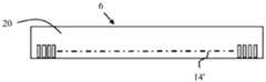
图1a至图1c示出了根据实施例的显示装置2及其组件。图1a示出了所述显示装置2的侧视图。所述显示装置2包括显示屏4、柔性线路(flexible printed circuit,简称FPC)8和显示集成电路(display integrated circuit,简称DIC)6。图1b示出了显示装置2的显示屏4的俯视图。图1c示出了FPC 8的视图。1a to 1c illustrate a
在图1a中,所述显示屏4被示出为包括第一层和第二层。然而,所述显示屏4还可仅包括一层或多于两层。所述第一层可以包括薄膜晶体管(thin-film-transistor,简称TFT)LCD玻璃面板等,所述第二层可以包括滤色镜和/或封装玻璃等。In Figure 1a, the
所述DIC 6用于驱动所述显示屏4。所述显示屏4可以包括LCD、LED或OLED等。所述DIC 6提供控制系统11和显示屏4之间的接口功能。所述DIC 6可以包括微控制器和存储器等。The
所述控制系统11可以是用户设备的控制系统11,其中的用户设备例如手机、平板电脑、笔记本电脑或类似产品。所述控制系统11可至少包括微处理器、微控制器、ASIC或类似部件。用户设备的控制系统11在图1a中用虚线示意性示出。例如,所述FPC 8可以经由一个或多个未示出的连接器连接到控制系统11。The
所述显示屏4包括第一电连接器12,参考图1b。在图1b中,仅示出了有限数量的第一电连接器12。第一电连接器12与设置在显示屏4的屏幕区域5中的电部件连接并且用于向设置在显示屏4的屏幕区域5中的电部件提供电信号。屏幕区域5中的电部件用于形成屏幕区域5的像素。像素集体地或成组地通过经由第一电连接器12发送的电信号形成在屏幕区域5中显示的信息。The
所述DIC 6包括第二电连接器,参考以下图2a至图2c。所述FPC 8包括第三电连接器16。参见图1c,图1c清楚地示出了所述FPC 8。也就是说,所述FPC 8包括柔性基板,如图1a的侧视图所示柔性基板是可弯曲的。在图1c中,仅示出了有限数量的第三电连接器16。所述第三电连接器16用于向所述DIC 6提供电信号。The
为了便于说明不同的部件及其布置,在图1a至图1c中不同部件的大小与实际的显示装置的大小有偏离。例如,在图1a的侧视图中所述DIC 6的宽度可以在1-3mm的范围内。In order to facilitate the description of the different components and their arrangement, the sizes of the different components in FIGS. 1 a to 1 c deviate from the size of the actual display device. For example, the width of the
所述DIC 6通过第一电连接器12和DIC 6的第二电连接器之间的电连接设置在所述显示屏4上,所述FPC 8通过DIC 6的第二电连接器和第三电连接器16之间的电连接设置在所述DIC 6上。The
在显示屏4上设置的DIC 6以及DIC 6上的FPC 8沿着显示屏4的边缘22为DIC 6和FPC 8提供了狭窄的连接。因此,显示屏的很大一部分可能会占用区域5。因此,可以在显示屏4的大部分表面上呈现信息。The
更具体地,所述显示屏4包括沿着显示屏4的边缘22延伸的第一表面部分10。所述第一表面部分10设置在显示屏4的屏幕区域5和边缘22之间。显示屏4的第一电连接器12设置在第一表面部分10处。因此,可以说第一表面部分10形成显示屏4的电连接部分。所述DIC6设置在第一表面部分10上。所述DIC 6安装并电连接到显示屏4的第一表面部分10。在显示屏4的第一电连接器12和DIC 6的第二电连接器之间提供电接触。More specifically, the
当安装在用户设备中时,FPC 8从DIC 6围绕显示屏4的边缘22延伸到显示屏4的第二侧9,第二侧9与显示屏4的第一侧7相对,而DIC 6设置在显示屏4上,如图1a所示。因此,所述显示装置2在用户设备中占用很小的空间。在显示屏4的第二侧9上,可以设置用户设备的控制系统11。When installed in the user equipment, the
图2a至图2c示出了显示集成电路(display integrated circuit,简称DIC)6的不同视图。所述DIC 6用于驱动用户设备的显示屏。所述DIC 6可以是形成显示装置2的一部分的DIC 6,如参考图1a至图1c所讨论的。FIGS. 2 a to 2 c show different views of a display integrated circuit (DIC) 6 . The
所述DIC 6包括主体15。所述主体15包括第一外表面18和与第一外表面18相对的第二外表面20。所述DIC 6还包括设置在主体15内部的处理器电路19和电连接器14、14'。在图2c中用虚线表示处理器电路19。所述电连接器14、14'在下文中称为第二电连接器14、14',从而可以清楚地理解它们在本文讨论的显示装置4中的功能。The
所述第二电连接器14、14'用于将DIC 6与显示屏4和另一个处理器电路电连接。所述另外的处理器电路可以形成用户设备的控制系统的一部分。The second
所述第二电连接器14、14′分别设置在第一外表面18和第二外表面20处。图2a示出了DIC 6的仰视图,其中第二电连接器14设置成两行。在第一外表面18处的第二电连接器14是第一电信号接口的第二电连接器14。图2b示出了DIC 6的俯视图,其中第二电连接器14′设置成一行。在所述第二外表面20处的第二电连接器14’是第二电信号接口的第二电连接器14’。The second
所述第二电信号接口的第二电连接器14’通过硅通孔(through silicon via,简称TSV)设置在第二外表面20上。因此,通常仅设置在集成电路一侧上的电连接器可以设置在DIC 6的两个相对侧。所述TSV是穿过DIC 6的硅片或芯片的垂直互连通道(verticalinterconnect access,简称VIA)。为了说明所述TSV,图2c示出了沿图2a中的C-C线通过DIC6的粗略示意性横截面。附图标记17表示TSV,其填充有导电材料,该导电材料从主体15内部的电子部件/电路延伸到设置在第二外表面20处的第二电信号接口的第二电连接器14’。The second electrical connector 14' of the second electrical signal interface is disposed on the second
因此,所述DIC 6用于经由位于第一外表面18的第一电信号接口的第二电连接器14连接至显示屏。此外,所述DIC 6用于经由位于第二外表面20的第二电信号接口的第二电连接器14'连接至FPC。更具体地,第一电信号接口的第二电连接器14用于连接到显示屏4的第一电连接器12,见图1a,第二电信号接口的第二电连接器14'用于连接到FPC 8的第三电连接器16,见图1c。Thus, the
图3示出了根据实施例的用户设备50。所述用户设备50可以是手机等。所述用户设备包括根据本文所讨论的任何一个方面和/或实施例中的显示装置2。例如,所述用户设备50可以包括根据结合图1a至图2c讨论的实施例的显示装置2。Figure 3 shows a
所述显示装置2的显示屏4在图3中用虚线表示。所述显示屏4的外边缘可能被用户设备50的外壳覆盖,因此,除非拆卸用户设备,否则它是不可见的。图3中示出了参考以上图1和图1b讨论的边缘22。图3中用实线示出了显示屏4的屏幕区域5,该部分在使用用户设备50时可见。The
所述显示装置2的显示屏4可以覆盖用户设备50的整个表面52的至少80%。根据一些实施例,所述显示屏4可以覆盖用户设备50的整个表面52的至少90%。The
更具体地,所述显示屏4的屏幕区域5可以覆盖用户设备50的整个表面52的至少80%。根据一些实施例,所述屏幕区域5可以覆盖用户设备50的整个表面52的至少90%。More specifically, the
图4示出了制造用户设备的显示装置的方法100。下面将参考图4以及参考图5a至图5c和图6a至图6c讨论所述方法100。FIG. 4 shows a
所述显示装置可以是根据本文所讨论的任何一个方面和/或实施例中的显示装置。例如,所述显示装置可以是根据结合图1a至图2c讨论的实施例的显示装置2。所述用户设备可以是根据本文所讨论的任何一个方面和/或实施例中的用户设备。所述用户设备可以是根据结合图3讨论的实施例的用户设备50。The display device may be a display device according to any of the aspects and/or embodiments discussed herein. For example, the display device may be the
因此,所述显示装置2包括显示屏4、用于驱动显示屏4的显示集成电路(displayintegrated circuit,简称DIC)6和柔性线路(flexible printed circuit,简称FPC)8。Therefore, the
所述方法100包括:The
-第一接合步骤102,其中所述DIC 6接合到所述显示屏4或所述FPC 8;- a first bonding step 102, wherein the
-第二接合步骤104,其中所述DIC 6接合到所述显示屏4和所述FPC 8中的另一个。- A second bonding step 104 in which the
所述第一接合步骤102和第二接合步骤104可以同时执行,也可以依次执行。The first bonding step 102 and the second bonding step 104 may be performed simultaneously or sequentially.
图5b和图6b示出了第一接合步骤102的实质。在图5b的实施例中,所述DIC 6在第一接合步骤102中接合到显示屏4。在图6b的实施例中,所述DIC 6在第一接合步骤102中接合到FPC 8。图5c和图6c示出了第二接合步骤104的实质。在图5c的实施例中,所述DIC 6在第二接合步骤104中接合到FPC 8。在图6c的实施例中,所述DIC 6在第二接合步骤104中接合到显示屏4。Figures 5b and 6b illustrate the essence of the first bonding step 102. In the embodiment of FIG. 5b , the
如果同时执行第一和第二接合步骤102、104,则可以说图5c和图6c示出了此类实施例。If the first and second joining steps 102, 104 are performed simultaneously, it can be said that Figures 5c and 6c show such an embodiment.
所述第一接合步骤102可以包括以下步骤:The first joining step 102 may include the following steps:
-步骤106:在平台60上支撑所述显示屏4或所述FPC 8。图5a和图6a示出了支撑步骤106的实施例。在图5a的实施例中,所述显示屏4被支撑在平台60上。在图6a的实施例中,所述FPC 8被支撑在平台60上。- Step 106 : supporting the
-步骤108:将所述DIC 6放置在显示屏4或FPC 8上,所述显示屏或FPC在步骤106中被支撑在所述平台60上。- Step 108 : placing the
-步骤110:向所述DIC 6施加压力。- Step 110 : Apply pressure to the
-步骤112:施加热量。- Step 112: Apply heat.
在步骤110的施加压力的步骤和步骤112的施加热量的步骤中,可以利用顶部62。步骤110的施加压力的步骤和步骤112的的施加热量的步骤可以至少部分同时进行。图5b和图6b中示出了步骤110的施加压力的步骤和步骤112的施加热量的步骤。In the step of applying pressure of step 110 and the step of applying heat of step 112, the
适当地,在第一接合步骤102中,在步骤112的施加热量的步骤中熔化的接合材料66分别设置在DIC 6和显示屏4之间,或者在DIC 6和FPC 8之间。Suitably, in the first bonding step 102, the
根据图5c所示的实施例,所述第二接合步骤104可以包括以下步骤:According to the embodiment shown in Fig. 5c, the second bonding step 104 may include the following steps:
-步骤114:在平台60上支撑所述显示屏。- Step 114 : supporting the display screen on the
-步骤116:如果在第一接合步骤102中将所述DIC 6接合到所述FPC 8,则将所述DIC 6放置在所述显示屏4上,或者- Step 116: If the
-步骤118:如果在第一接合步骤102中将所述DIC 6接合到所述显示屏4,则将所述FPC8放置在所述DIC 6上。- Step 118 : If the
-步骤120:向所述FPC 8施加压力。- Step 120: Apply pressure to the
-步骤122:施加热量。- Step 122: Apply heat.
在步骤120的施加压力的步骤和步骤122的施加热量的步骤中,可以利用顶部62。施加压力和施加热量的步骤可以至少部分同时进行。在图5c中,示出了在DIC 6和FPC 8之间的在施加热量步骤期间熔化的接合材料68。这在步骤118中将FPC 8放置在DIC 6上的步骤中适用。当然,如果改为执行步骤116中放置DIC 6的步骤,则在显示屏4和DIC 6之间设置在施加热量步骤期间熔化的接合材料。In the step of applying pressure of step 120 and the step of applying heat of step 122, the
根据图6c所示的实施例,所述第二接合步骤104可以包括以下步骤:According to the embodiment shown in FIG. 6c, the second bonding step 104 may include the following steps:
-步骤124:在平台60上支撑所述FPC 8;- Step 124: supporting the
-步骤126:如果在第一接合步骤102中将所述DIC 6接合到所述显示屏4,则将所述DIC6放置在所述FPC 8上,或者- Step 126: If the
-步骤128:如果在第一接合步骤102中将所述DIC 6接合到所述FPC 8,则将所述显示屏4放置在所述DIC 6上;- Step 128: if the
-步骤130:向所述显示屏4施加压力;- Step 130: applying pressure to the
-步骤132:施加热量。- Step 132: Applying heat.
在步骤130的施加压力的步骤和步骤132的施加热量的步骤中,可以利用顶部62。施加压力和施加热量的步骤可以至少部分同时进行。在图6c中,示出了在显示屏4和DIC 6之间的在施加热量步骤期间熔化的接合材料70。这在步骤128中将显示屏4放置在DIC 6上的步骤中适用。当然,如果改为执行步骤126中的在FPC 8上放置DIC 6的步骤,则在DIC 6和FPC 8之间设置在施加热量步骤期间熔化的接合材料。In the step of applying pressure of step 130 and the step of applying heat of step 132, the
所述平台60在施加压力和施加热量的步骤中形成支撑。在施加热量的步骤中,可以从平台60施加热量,或者通过平台60施加热量。可以在施加压力和施加热量的不同步骤中使用同一平台60。或者,可以在施加压力和施加热量的不同步骤中使用不同平台60。The
所述顶部62在施加压力和施加热量的步骤中形成可移动装置。因此,为了将相关部件放置在平台60上,所述顶部62远离平台60移动。为了施加压力,所述顶部62按照图5b、5c、6b、6c中的箭头指示朝着相关部件移动。在施加热量的步骤中,可以从顶部62施加热量,或者通过顶部62施加热量。可以在施加压力和施加热量的不同步骤中使用同一顶部62。或者,可以在施加压力和施加热量的不同步骤中使用不同顶部62。The top 62 forms a movable device during the steps of applying pressure and applying heat. Therefore, in order to place the relevant components on the
在第一接合步骤102中使用的接合材料66可以具有比在第二接合步骤104中使用的接合材料68、70更高的熔点。The
因此,在所述第一接合步骤102的施加热量的步骤112中施加的温度高于在所述第二接合步骤104的施加热量的步骤122、132中施加的温度。通过这种方式,在所述第一接合步骤102中创建的接合在第二接合步骤104中不会解除接合。Therefore, the temperature applied in the heat applying step 112 of the first bonding step 102 is higher than the temperature applied in the heat applying steps 122 , 132 of the second bonding step 104 . In this way, the bond created in the first bonding step 102 is not disengaged in the second bonding step 104 .
在所述第一接合步骤102和所述第二接合步骤104的至少一个中,可以使用各向异性导电膜(anisotropic conductive film,简称ACF)。因此,接合材料66、68、70中的一种或两种可以包括ACF。当接合时,ACF在第一、第二和第三电导体12、14、16之间提供电连接。ACF可以具有不同的熔点。因此,接合材料66、68、70可以具有不同的熔点。In at least one of the first bonding step 102 and the second bonding step 104 , an anisotropic conductive film (ACF for short) may be used. Thus, one or both of the
在图5a中示出了参考以上图1a和图1b讨论的沿着显示屏4的边缘22延伸的第一表面部分10。如果所述DIC 6在第一接合步骤102中接合到所述显示屏4,则所述DIC 6在第一接合步骤102中接合到所述第一表面部分10;如果所述DIC 6在第二接合步骤104中接合到所述显示屏4,则所述DIC 6在第二接合步骤104中接合到所述第一表面部分10。The
应当理解,前述内容是各种示例实施例的说明,并且保护范围仅由所附权利要求限定。本领域技术人员将意识到,示例实施例可以被修改,并且示例实施例的不同特征可以被组合以创建不同于本文所述实施例的实施例。It is to be understood that the foregoing is an illustration of various example embodiments, and that the scope of protection is limited only by the appended claims. Those skilled in the art will appreciate that example embodiments may be modified and different features of example embodiments may be combined to create embodiments other than those described herein.
Claims (15)
Translated fromChineseApplications Claiming Priority (1)
| Application Number | Priority Date | Filing Date | Title |
|---|---|---|---|
| PCT/EP2017/080338WO2019101329A1 (en) | 2017-11-24 | 2017-11-24 | Display arrangement and thereto related integrated circuit and method and user equipment |
Publications (1)
| Publication Number | Publication Date |
|---|---|
| CN111527536Atrue CN111527536A (en) | 2020-08-11 |
Family
ID=60629667
Family Applications (1)
| Application Number | Title | Priority Date | Filing Date |
|---|---|---|---|
| CN201780095864.8APendingCN111527536A (en) | 2017-11-24 | 2017-11-24 | Display device and related integrated circuit, method and user equipment thereof |
Country Status (4)
| Country | Link |
|---|---|
| US (1) | US20200363845A1 (en) |
| EP (1) | EP3692518A1 (en) |
| CN (1) | CN111527536A (en) |
| WO (1) | WO2019101329A1 (en) |
Citations (9)
| Publication number | Priority date | Publication date | Assignee | Title |
|---|---|---|---|---|
| CN101211043A (en)* | 2006-12-27 | 2008-07-02 | Lg.菲利浦Lcd株式会社 | Liquid crystal display device and manufacturing method thereof |
| CN102800797A (en)* | 2011-05-24 | 2012-11-28 | 台湾积体电路制造股份有限公司 | Batwing led with remote phosphor configuration |
| CN103842898A (en)* | 2011-10-05 | 2014-06-04 | 苹果公司 | Interconnection schemes for displays with minimized border regions |
| CN103887314A (en)* | 2012-12-21 | 2014-06-25 | 乐金显示有限公司 | Flexible Display And Method For Manufacturing The Same |
| CN105869558A (en)* | 2015-02-05 | 2016-08-17 | 三星显示有限公司 | Display device |
| US20160351586A1 (en)* | 2015-05-28 | 2016-12-01 | Samsung Display Co., Ltd. | Display device |
| US20170025399A1 (en)* | 2015-07-23 | 2017-01-26 | Seoul Semiconductor Co., Ltd. | Display apparatus and manufacturing method thereof |
| CN107004774A (en)* | 2014-12-11 | 2017-08-01 | 乐金显示有限公司 | Flexible display device with corrosion-resistant printed circuit film |
| CN107247372A (en)* | 2017-07-24 | 2017-10-13 | 武汉华星光电技术有限公司 | A kind of display device and Intelligent mobile equipment |
Family Cites Families (8)
| Publication number | Priority date | Publication date | Assignee | Title |
|---|---|---|---|---|
| US6292248B1 (en)* | 1997-08-09 | 2001-09-18 | Lg. Philips Lcd Co., Ltd. | COG type liquid crystal panel and fabrication method thereof having first and second conductive bumps in different planes |
| JP3371873B2 (en)* | 1999-12-22 | 2003-01-27 | 日本電気株式会社 | Liquid crystal display device and adjustment method thereof |
| KR20020027958A (en) | 2000-10-06 | 2002-04-15 | 구자홍 | COF structure of display device |
| JP6448391B2 (en)* | 2015-01-28 | 2019-01-09 | 株式会社ジャパンディスプレイ | Display module |
| JP2016188976A (en)* | 2015-03-30 | 2016-11-04 | 株式会社ジャパンディスプレイ | Display device |
| JP6531033B2 (en)* | 2015-11-24 | 2019-06-12 | 株式会社ジャパンディスプレイ | Display device |
| WO2017191957A1 (en)* | 2016-05-02 | 2017-11-09 | 삼성전자 주식회사 | Screen display method and electronic device supporting same |
| CN107329335B (en)* | 2017-06-21 | 2020-02-28 | 武汉华星光电技术有限公司 | Array substrate and display panel |
- 2017
- 2017-11-24CNCN201780095864.8Apatent/CN111527536A/enactivePending
- 2017-11-24WOPCT/EP2017/080338patent/WO2019101329A1/ennot_activeCeased
- 2017-11-24EPEP17811502.8Apatent/EP3692518A1/ennot_activeCeased
- 2017-11-24USUS16/766,579patent/US20200363845A1/ennot_activeAbandoned
Patent Citations (9)
| Publication number | Priority date | Publication date | Assignee | Title |
|---|---|---|---|---|
| CN101211043A (en)* | 2006-12-27 | 2008-07-02 | Lg.菲利浦Lcd株式会社 | Liquid crystal display device and manufacturing method thereof |
| CN102800797A (en)* | 2011-05-24 | 2012-11-28 | 台湾积体电路制造股份有限公司 | Batwing led with remote phosphor configuration |
| CN103842898A (en)* | 2011-10-05 | 2014-06-04 | 苹果公司 | Interconnection schemes for displays with minimized border regions |
| CN103887314A (en)* | 2012-12-21 | 2014-06-25 | 乐金显示有限公司 | Flexible Display And Method For Manufacturing The Same |
| CN107004774A (en)* | 2014-12-11 | 2017-08-01 | 乐金显示有限公司 | Flexible display device with corrosion-resistant printed circuit film |
| CN105869558A (en)* | 2015-02-05 | 2016-08-17 | 三星显示有限公司 | Display device |
| US20160351586A1 (en)* | 2015-05-28 | 2016-12-01 | Samsung Display Co., Ltd. | Display device |
| US20170025399A1 (en)* | 2015-07-23 | 2017-01-26 | Seoul Semiconductor Co., Ltd. | Display apparatus and manufacturing method thereof |
| CN107247372A (en)* | 2017-07-24 | 2017-10-13 | 武汉华星光电技术有限公司 | A kind of display device and Intelligent mobile equipment |
Also Published As
| Publication number | Publication date |
|---|---|
| EP3692518A1 (en) | 2020-08-12 |
| US20200363845A1 (en) | 2020-11-19 |
| WO2019101329A1 (en) | 2019-05-31 |
Similar Documents
| Publication | Publication Date | Title |
|---|---|---|
| CN109616480B (en) | Display panel and display device | |
| US12313944B2 (en) | Display device and method for manufacturing same | |
| CN202887620U (en) | Flexible display panel and display device including the same | |
| US9836161B2 (en) | Touch sensor built-in display device structure | |
| TW201735616A (en) | Display device | |
| CN102855822A (en) | Flexible display panel and display apparatus including the flexible display panel | |
| US10431141B2 (en) | Display device | |
| KR102600528B1 (en) | Display device | |
| KR102517911B1 (en) | Display device | |
| KR102810501B1 (en) | Display device | |
| CN111724707A (en) | display device | |
| KR20140121178A (en) | Chip-on-film package and device assembly including the same | |
| CN111430421A (en) | Display device and method of manufacturing the same | |
| CN111403934B (en) | Display device | |
| KR20180035270A (en) | Tape carrier package and display device having the same | |
| CN107526221B (en) | Display device for preventing static electricity flow | |
| CN111722745B (en) | Display device | |
| KR102417789B1 (en) | Flexible display device | |
| US11409335B2 (en) | Display device | |
| CN111527536A (en) | Display device and related integrated circuit, method and user equipment thereof | |
| CN114677987B (en) | Display panel and display device | |
| KR20190085196A (en) | Display device | |
| CN108364996A (en) | O L ED display device | |
| TWI857791B (en) | Circuit substrate | |
| CN109857270B (en) | Touch control display device |
Legal Events
| Date | Code | Title | Description |
|---|---|---|---|
| PB01 | Publication | ||
| PB01 | Publication | ||
| SE01 | Entry into force of request for substantive examination | ||
| SE01 | Entry into force of request for substantive examination | ||
| RJ01 | Rejection of invention patent application after publication | Application publication date:20200811 | |
| RJ01 | Rejection of invention patent application after publication |