CN111524974B - Semiconductor device and manufacturing method thereof - Google Patents
Semiconductor device and manufacturing method thereofDownload PDFInfo
- Publication number
- CN111524974B CN111524974BCN202010054768.2ACN202010054768ACN111524974BCN 111524974 BCN111524974 BCN 111524974BCN 202010054768 ACN202010054768 ACN 202010054768ACN 111524974 BCN111524974 BCN 111524974B
- Authority
- CN
- China
- Prior art keywords
- layer
- gate
- dielectric
- metal
- semiconductor device
- Prior art date
- Legal status (The legal status is an assumption and is not a legal conclusion. Google has not performed a legal analysis and makes no representation as to the accuracy of the status listed.)
- Active
Links
Images


Classifications
- H—ELECTRICITY
- H10—SEMICONDUCTOR DEVICES; ELECTRIC SOLID-STATE DEVICES NOT OTHERWISE PROVIDED FOR
- H10D—INORGANIC ELECTRIC SEMICONDUCTOR DEVICES
- H10D64/00—Electrodes of devices having potential barriers
- H10D64/20—Electrodes characterised by their shapes, relative sizes or dispositions
- H10D64/27—Electrodes not carrying the current to be rectified, amplified, oscillated or switched, e.g. gates
- H10D64/311—Gate electrodes for field-effect devices
- H10D64/411—Gate electrodes for field-effect devices for FETs
- H10D64/511—Gate electrodes for field-effect devices for FETs for IGFETs
- H10D64/517—Gate electrodes for field-effect devices for FETs for IGFETs characterised by the conducting layers
- H10D64/518—Gate electrodes for field-effect devices for FETs for IGFETs characterised by the conducting layers characterised by their lengths or sectional shapes
- H—ELECTRICITY
- H10—SEMICONDUCTOR DEVICES; ELECTRIC SOLID-STATE DEVICES NOT OTHERWISE PROVIDED FOR
- H10D—INORGANIC ELECTRIC SEMICONDUCTOR DEVICES
- H10D62/00—Semiconductor bodies, or regions thereof, of devices having potential barriers
- H10D62/80—Semiconductor bodies, or regions thereof, of devices having potential barriers characterised by the materials
- H10D62/83—Semiconductor bodies, or regions thereof, of devices having potential barriers characterised by the materials being Group IV materials, e.g. B-doped Si or undoped Ge
- H—ELECTRICITY
- H10—SEMICONDUCTOR DEVICES; ELECTRIC SOLID-STATE DEVICES NOT OTHERWISE PROVIDED FOR
- H10D—INORGANIC ELECTRIC SEMICONDUCTOR DEVICES
- H10D30/00—Field-effect transistors [FET]
- H10D30/01—Manufacture or treatment
- H10D30/021—Manufacture or treatment of FETs having insulated gates [IGFET]
- H10D30/027—Manufacture or treatment of FETs having insulated gates [IGFET] of lateral single-gate IGFETs
- H—ELECTRICITY
- H10—SEMICONDUCTOR DEVICES; ELECTRIC SOLID-STATE DEVICES NOT OTHERWISE PROVIDED FOR
- H10D—INORGANIC ELECTRIC SEMICONDUCTOR DEVICES
- H10D30/00—Field-effect transistors [FET]
- H10D30/01—Manufacture or treatment
- H10D30/021—Manufacture or treatment of FETs having insulated gates [IGFET]
- H10D30/031—Manufacture or treatment of FETs having insulated gates [IGFET] of thin-film transistors [TFT]
- H10D30/0321—Manufacture or treatment of FETs having insulated gates [IGFET] of thin-film transistors [TFT] comprising silicon, e.g. amorphous silicon or polysilicon
- H10D30/0323—Manufacture or treatment of FETs having insulated gates [IGFET] of thin-film transistors [TFT] comprising silicon, e.g. amorphous silicon or polysilicon comprising monocrystalline silicon
- H—ELECTRICITY
- H10—SEMICONDUCTOR DEVICES; ELECTRIC SOLID-STATE DEVICES NOT OTHERWISE PROVIDED FOR
- H10D—INORGANIC ELECTRIC SEMICONDUCTOR DEVICES
- H10D30/00—Field-effect transistors [FET]
- H10D30/60—Insulated-gate field-effect transistors [IGFET]
- H—ELECTRICITY
- H10—SEMICONDUCTOR DEVICES; ELECTRIC SOLID-STATE DEVICES NOT OTHERWISE PROVIDED FOR
- H10D—INORGANIC ELECTRIC SEMICONDUCTOR DEVICES
- H10D30/00—Field-effect transistors [FET]
- H10D30/60—Insulated-gate field-effect transistors [IGFET]
- H10D30/67—Thin-film transistors [TFT]
- H10D30/6729—Thin-film transistors [TFT] characterised by the electrodes
- H10D30/6737—Thin-film transistors [TFT] characterised by the electrodes characterised by the electrode materials
- H10D30/6739—Conductor-insulator-semiconductor electrodes
- H—ELECTRICITY
- H10—SEMICONDUCTOR DEVICES; ELECTRIC SOLID-STATE DEVICES NOT OTHERWISE PROVIDED FOR
- H10D—INORGANIC ELECTRIC SEMICONDUCTOR DEVICES
- H10D30/00—Field-effect transistors [FET]
- H10D30/60—Insulated-gate field-effect transistors [IGFET]
- H10D30/67—Thin-film transistors [TFT]
- H10D30/674—Thin-film transistors [TFT] characterised by the active materials
- H10D30/6741—Group IV materials, e.g. germanium or silicon carbide
- H10D30/6743—Silicon
- H10D30/6744—Monocrystalline silicon
- H—ELECTRICITY
- H10—SEMICONDUCTOR DEVICES; ELECTRIC SOLID-STATE DEVICES NOT OTHERWISE PROVIDED FOR
- H10D—INORGANIC ELECTRIC SEMICONDUCTOR DEVICES
- H10D64/00—Electrodes of devices having potential barriers
- H10D64/01—Manufacture or treatment
- H10D64/017—Manufacture or treatment using dummy gates in processes wherein at least parts of the final gates are self-aligned to the dummy gates, i.e. replacement gate processes
- H—ELECTRICITY
- H10—SEMICONDUCTOR DEVICES; ELECTRIC SOLID-STATE DEVICES NOT OTHERWISE PROVIDED FOR
- H10D—INORGANIC ELECTRIC SEMICONDUCTOR DEVICES
- H10D64/00—Electrodes of devices having potential barriers
- H10D64/01—Manufacture or treatment
- H10D64/018—Spacers formed inside holes at the prospective gate locations, e.g. holes left by removing dummy gates
- H—ELECTRICITY
- H10—SEMICONDUCTOR DEVICES; ELECTRIC SOLID-STATE DEVICES NOT OTHERWISE PROVIDED FOR
- H10D—INORGANIC ELECTRIC SEMICONDUCTOR DEVICES
- H10D64/00—Electrodes of devices having potential barriers
- H10D64/01—Manufacture or treatment
- H10D64/021—Manufacture or treatment using multiple gate spacer layers, e.g. bilayered sidewall spacers
- H—ELECTRICITY
- H10—SEMICONDUCTOR DEVICES; ELECTRIC SOLID-STATE DEVICES NOT OTHERWISE PROVIDED FOR
- H10D—INORGANIC ELECTRIC SEMICONDUCTOR DEVICES
- H10D64/00—Electrodes of devices having potential barriers
- H10D64/60—Electrodes characterised by their materials
- H10D64/62—Electrodes ohmically coupled to a semiconductor
- H—ELECTRICITY
- H10—SEMICONDUCTOR DEVICES; ELECTRIC SOLID-STATE DEVICES NOT OTHERWISE PROVIDED FOR
- H10D—INORGANIC ELECTRIC SEMICONDUCTOR DEVICES
- H10D64/00—Electrodes of devices having potential barriers
- H10D64/60—Electrodes characterised by their materials
- H10D64/66—Electrodes having a conductor capacitively coupled to a semiconductor by an insulator, e.g. MIS electrodes
- H10D64/665—Electrodes having a conductor capacitively coupled to a semiconductor by an insulator, e.g. MIS electrodes the conductor comprising a layer of elemental metal contacting the insulator, e.g. tungsten or molybdenum
- H10D64/666—Electrodes having a conductor capacitively coupled to a semiconductor by an insulator, e.g. MIS electrodes the conductor comprising a layer of elemental metal contacting the insulator, e.g. tungsten or molybdenum the conductor further comprising additional layers
- H—ELECTRICITY
- H10—SEMICONDUCTOR DEVICES; ELECTRIC SOLID-STATE DEVICES NOT OTHERWISE PROVIDED FOR
- H10D—INORGANIC ELECTRIC SEMICONDUCTOR DEVICES
- H10D64/00—Electrodes of devices having potential barriers
- H10D64/60—Electrodes characterised by their materials
- H10D64/66—Electrodes having a conductor capacitively coupled to a semiconductor by an insulator, e.g. MIS electrodes
- H10D64/667—Electrodes having a conductor capacitively coupled to a semiconductor by an insulator, e.g. MIS electrodes the conductor comprising a layer of alloy material, compound material or organic material contacting the insulator, e.g. TiN workfunction layers
- H—ELECTRICITY
- H10—SEMICONDUCTOR DEVICES; ELECTRIC SOLID-STATE DEVICES NOT OTHERWISE PROVIDED FOR
- H10D—INORGANIC ELECTRIC SEMICONDUCTOR DEVICES
- H10D64/00—Electrodes of devices having potential barriers
- H10D64/60—Electrodes characterised by their materials
- H10D64/66—Electrodes having a conductor capacitively coupled to a semiconductor by an insulator, e.g. MIS electrodes
- H10D64/68—Electrodes having a conductor capacitively coupled to a semiconductor by an insulator, e.g. MIS electrodes characterised by the insulator, e.g. by the gate insulator
- H10D64/681—Electrodes having a conductor capacitively coupled to a semiconductor by an insulator, e.g. MIS electrodes characterised by the insulator, e.g. by the gate insulator having a compositional variation, e.g. multilayered
- H10D64/685—Electrodes having a conductor capacitively coupled to a semiconductor by an insulator, e.g. MIS electrodes characterised by the insulator, e.g. by the gate insulator having a compositional variation, e.g. multilayered being perpendicular to the channel plane
- H—ELECTRICITY
- H10—SEMICONDUCTOR DEVICES; ELECTRIC SOLID-STATE DEVICES NOT OTHERWISE PROVIDED FOR
- H10D—INORGANIC ELECTRIC SEMICONDUCTOR DEVICES
- H10D64/00—Electrodes of devices having potential barriers
- H10D64/60—Electrodes characterised by their materials
- H10D64/66—Electrodes having a conductor capacitively coupled to a semiconductor by an insulator, e.g. MIS electrodes
- H10D64/68—Electrodes having a conductor capacitively coupled to a semiconductor by an insulator, e.g. MIS electrodes characterised by the insulator, e.g. by the gate insulator
- H10D64/691—Electrodes having a conductor capacitively coupled to a semiconductor by an insulator, e.g. MIS electrodes characterised by the insulator, e.g. by the gate insulator comprising metallic compounds, e.g. metal oxides or metal silicates
Landscapes
- Insulated Gate Type Field-Effect Transistor (AREA)
- Electrodes Of Semiconductors (AREA)
- Thin Film Transistor (AREA)
Abstract
Description
Translated fromChinese技术领域technical field
本发明的实施例是有关于半导体器件及其制造方法。Embodiments of the present invention relate to semiconductor devices and methods of manufacturing the same.
背景技术Background technique
许多现代电子器件含有金属氧化物半导体场效应晶体管(metal-oxide-semiconductor field-effect transistor,MOSFET)。MOSFET具有布置在源极区与漏极区之间的衬底之上的栅极结构。施加到栅极结构的栅极电极的电压决定MOSFET的导电性。高介电常数金属栅极(high-κmetal gate,HKMG)技术由于具有按比例缩放(scaling)的优势而有望成为下一代MOSFET器件的候选项。Many modern electronic devices contain metal-oxide-semiconductor field-effect transistors (MOSFETs). A MOSFET has a gate structure disposed over a substrate between a source region and a drain region. The voltage applied to the gate electrode of the gate structure determines the conductivity of the MOSFET. High-k metal gate (HKMG) technology is expected to be a candidate for next-generation MOSFET devices due to its scaling advantages.
发明内容Contents of the invention
在一些实施例中,本申请提供一种半导体器件,所述半导体器件包括:一对间隔件段,位于半导体衬底上;高介电常数栅极介电结构,上覆在所述半导体衬底上,其中所述高介电常数栅极介电结构在横向上位于所述间隔件段之间且与所述间隔件段相邻;以及栅极结构,位于所述高介电常数栅极介电结构之上且具有与所述间隔件段的顶表面大约齐平的顶表面,其中所述栅极结构包括金属结构及栅极本体层,其中所述栅极本体层具有相对于所述金属结构的顶表面在垂直方向上偏置的顶表面且还具有被所述金属结构以杯状包围的下部部分。In some embodiments, the present application provides a semiconductor device comprising: a pair of spacer segments on a semiconductor substrate; a high-k gate dielectric structure overlying the semiconductor substrate wherein the high-k gate dielectric structure is laterally located between and adjacent to the spacer segments; and a gate structure located between the high-k gate dielectric structures and having a top surface approximately flush with the top surface of the spacer segment, wherein the gate structure includes a metal structure and a gate body layer, wherein the gate body layer has a The top surface is vertically offset and also has a lower portion cupped by the metal structure.
在一些实施例中,本申请提供一种半导体器件,所述半导体器件包括:一对源极/漏极区,位于半导体衬底中;高介电常数栅极介电结构,上覆在所述半导体衬底上,其中所述高介电常数栅极介电结构在横向上位于所述源极/漏极区之间且与所述源极/漏极区相邻;以及栅极结构,上覆在所述高介电常数栅极介电结构上,其中所述栅极结构包括堆叠在一起的栅极本体层与硅化物层,其中所述栅极结构还包括功函数结构,所述功函数结构包绕在所述栅极本体层的底部周围且沿着所述栅极本体层的侧壁及所述硅化物层的侧壁延伸到所述功函数结构的顶表面,且其中所述功函数结构的所述顶表面与所述硅化物层的顶表面大约齐平。In some embodiments, the present application provides a semiconductor device, which includes: a pair of source/drain regions located in a semiconductor substrate; a high dielectric constant gate dielectric structure overlying the On a semiconductor substrate, wherein the high-k gate dielectric structure is laterally located between and adjacent to the source/drain regions; and a gate structure, on overlying on the high dielectric constant gate dielectric structure, wherein the gate structure includes a gate body layer and a silicide layer stacked together, wherein the gate structure further includes a work function structure, and the work function The function structure is wrapped around the bottom of the gate body layer and extends along the sidewalls of the gate body layer and the sidewalls of the silicide layer to the top surface of the work function structure, and wherein the The top surface of the work function structure is approximately level with the top surface of the suicide layer.
在一些实施例中,本申请提供一种制造半导体器件的方法,所述方法包括:在半导体衬底之上形成虚设栅极结构,其中所述虚设栅极结构包括上覆在所述半导体衬底上的高介电常数栅极介电结构且还包括上覆在所述高介电常数栅极介电结构上的虚设栅极电极,且其中侧壁间隔件环绕所述虚设栅极结构;使用栅极电极层堆叠置换所述虚设栅极电极,其中所述栅极电极层堆叠包括金属层及上覆在所述金属层上的多晶硅层;将所述多晶硅层的上部部分转换成硅化物层;以及对所述栅极电极层堆叠及所述硅化物层执行平坦化工艺直到暴露出所述侧壁间隔件的上表面,从而界定栅极电极结构,其中所述平坦化工艺局部地移除所述硅化物层。In some embodiments, the present application provides a method of manufacturing a semiconductor device, the method comprising: forming a dummy gate structure over a semiconductor substrate, wherein the dummy gate structure includes and further comprising a dummy gate electrode overlying the high-k gate dielectric structure, and wherein sidewall spacers surround the dummy gate structure; using a gate electrode layer stack replacing the dummy gate electrode, wherein the gate electrode layer stack includes a metal layer and a polysilicon layer overlying the metal layer; converting an upper portion of the polysilicon layer into a silicide layer and performing a planarization process on the gate electrode layer stack and the silicide layer until upper surfaces of the sidewall spacers are exposed, thereby defining a gate electrode structure, wherein the planarization process locally removes The silicide layer.
附图说明Description of drawings
结合附图阅读以下详细说明,会最好地理解本公开的各个方面。应注意,根据本行业中的标准惯例,各种特征并非按比例绘制。事实上,为使论述清晰起见,可任意增大或减小各种特征的尺寸。Aspects of the present disclosure are best understood from the following detailed description when read with the accompanying figures. It should be noted that, in accordance with the standard practice in the industry, various features are not drawn to scale. In fact, the dimensions of the various features may be arbitrarily increased or reduced for clarity of discussion.
图1示出半导体器件的一些实施例的剖视图,所述半导体器件包括环绕硅化物层且上覆在高介电常数栅极介电结构上的功函数结构。1 illustrates a cross-sectional view of some embodiments of a semiconductor device including a work function structure surrounding a suicide layer and overlying a high-k gate dielectric structure.
图2示出图1所示半导体器件的一些更详细实施例的剖视图,其中功函数结构包括金属层堆叠,且高介电常数栅极介电结构包括介电层堆叠。2 illustrates cross-sectional views of some more detailed embodiments of the semiconductor device shown in FIG. 1 , wherein the work function structure includes a metal layer stack, and the high-k gate dielectric structure includes a dielectric layer stack.
图3A到图3C示出图2所示半导体器件的一些替代实施例的各个剖视图。3A to 3C illustrate various cross-sectional views of some alternative embodiments of the semiconductor device shown in FIG. 2 .
图4到图9示出形成半导体器件的第一方法的各种实施例的剖视图,所述半导体器件包括环绕硅化物层且上覆在高介电常数栅极介电结构上的功函数结构。4-9 illustrate cross-sectional views of various embodiments of a first method of forming a semiconductor device including a work function structure surrounding a suicide layer and overlying a high-k gate dielectric structure.
图10以流程图格式示出一种方法,所述流程图格式示出形成半导体器件的第一方法的一些实施例,所述半导体器件包括环绕硅化物层且上覆在高介电常数栅极介电结构上的功函数结构。FIG. 10 illustrates a method in flow chart format illustrating some embodiments of a first method of forming a semiconductor device including a surrounding suicide layer overlying a high-permittivity gate Work function structures on dielectric structures.
图11到图18示出形成半导体器件的第二方法的各种实施例的剖视图,所述半导体器件包括上覆在高介电常数栅极介电结构上的栅极结构。11-18 illustrate cross-sectional views of various embodiments of a second method of forming a semiconductor device including a gate structure overlying a high-k gate dielectric structure.
图19以流程图格式示出一种方法,所述流程图格式示出形成半导体器件的第二方法的一些实施例,所述半导体器件包括上覆在高介电常数栅极介电结构上的栅极结构。FIG. 19 illustrates a method in flowchart format illustrating some embodiments of a second method of forming a semiconductor device including an overlying high-k gate dielectric structure. grid structure.
具体实施方式Detailed ways
本公开提供用于实施本公开的不同特征的许多不同实施例或实例。以下阐述组件及布置的具体实例以简化本公开。当然,这些仅为实例且不旨在进行限制。举例来说,以下说明中将第一特征形成在第二特征“之上”或第二特征“上”可包括其中第一特征与第二特征被形成为直接接触的实施例,且也可包括其中第一特征与第二特征之间可形成有附加特征以使得所述第一特征与所述第二特征可不直接接触的实施例。另外,本公开可在各种实例中重复使用参考编号和/或字母。这种重复使用是出于简洁及清晰的目的,而不是自身表示所论述的各种实施例和/或配置之间的关系。The present disclosure provides many different embodiments, or examples, for implementing different features of the disclosure. Specific examples of components and arrangements are set forth below to simplify the present disclosure. Of course, these are examples only and are not intended to be limiting. For example, the description below that a first feature is formed "on" a second feature or "on" a second feature may include embodiments in which the first and second features are formed in direct contact, and may also include Embodiments wherein an additional feature may be formed between a first feature and a second feature such that the first feature and the second feature may not be in direct contact. Additionally, this disclosure may repeat reference numbers and/or letters in various instances. Such re-use is for brevity and clarity and does not in itself indicate a relationship between the various embodiments and/or configurations discussed.
此外,为易于说明,本文中可能使用例如“在…之下(beneath)”、“在…下方(below)”、“下部的(lower)”、“在…上方(above)”、“上部的(upper)”等空间相对性用语来阐述图中所示的一个元件或特征与另一(其他)元件或特征的关系。所述空间相对性用语旨在除图中所绘示的取向外还囊括器件在使用或操作中的不同取向。装置可具有其他取向(旋转90度或处于其他取向),且本文中所使用的空间相对性描述语可同样相应地进行解释。In addition, for ease of description, for example, "beneath", "below", "lower", "above", "upper" may be used herein (upper)" and other spatially relative terms are used to describe the relationship between one element or feature and another (other) element or feature shown in the figure. The spatially relative terms are intended to encompass different orientations of the device in use or operation in addition to the orientation depicted in the figures. The device may be at other orientations (rotated 90 degrees or at other orientations) and the spatially relative descriptors used herein interpreted accordingly.
在过去二十年里,MOSFET通常使用包含多晶硅的栅极结构。近年来,高介电常数金属栅极(HKMG)金属氧化物半导体场效应晶体管(MOSFET)由于性能改善及按比例缩放而开始得到广泛使用。在一些实施例中,在HKMG晶体管的栅极电极制作期间,在衬底上形成虚设栅极结构,且分别沿着虚设栅极结构的相对的侧壁形成源极及漏极区。虚设栅极结构包括虚设栅极电极,且还包括位于虚设栅极电极之下的高介电常数栅极介电层。形成覆盖虚设栅极结构的层间介电(inter-level dielectric,ILD)结构,且对ILD结构执行第一平坦化工艺(例如,化学机械平坦化(chemical mechanical planarization,CMP)工艺)直到暴露出虚设栅极结构。移除虚设栅极电极,从而暴露出高介电常数栅极介电层,且形成覆盖ILD结构且对通过移除所得的开口进行衬垫的金属层堆叠。执行第二平坦化工艺以移除金属层堆叠的位于开口外部的一部分。执行刻蚀工艺以对金属层堆叠的顶表面进行回蚀并局部地清除开口。形成在金属层堆叠之上填充开口的多晶硅层。执行第三平坦化工艺以移除多晶硅层的位于开口外部的一部分,且使多晶硅层的剩余部分硅化,从而在金属层堆叠之上形成硅化物层。这部分地界定了HKMG晶体管的栅极电极。在硅化物层之上且也在源极及漏极区之上设置导电接触件。随后在导电接触件之上的内连介电结构内形成上覆的金属线。For the past two decades, MOSFETs have typically used gate structures comprising polysilicon. In recent years, high-k metal-gate (HKMG) metal-oxide-semiconductor field-effect transistors (MOSFETs) have come into widespread use due to improved performance and scaling. In some embodiments, during fabrication of the gate electrode of the HKMG transistor, a dummy gate structure is formed on the substrate, and source and drain regions are formed along opposite sidewalls of the dummy gate structure, respectively. The dummy gate structure includes a dummy gate electrode, and further includes a high-k gate dielectric layer under the dummy gate electrode. forming an inter-level dielectric (inter-level dielectric, ILD) structure covering the dummy gate structure, and performing a first planarization process (for example, a chemical mechanical planarization (CMP) process) on the ILD structure until exposed dummy gate structure. The dummy gate electrode is removed, exposing the high-k gate dielectric layer, and forming a metal layer stack covering the ILD structure and lining the opening resulting from the removal. A second planarization process is performed to remove a portion of the metal layer stack outside the opening. An etch process is performed to etch back the top surface of the metal layer stack and partially remove the openings. A polysilicon layer filling the opening is formed over the metal layer stack. A third planarization process is performed to remove a portion of the polysilicon layer outside the opening and silicide the remaining portion of the polysilicon layer to form a silicide layer over the metal layer stack. This partially defines the gate electrode of the HKMG transistor. Conductive contacts are disposed over the silicide layer and also over the source and drain regions. Overlying metal lines are then formed within the interconnect dielectric structure over the conductive contacts.
上述方法的挑战在于所述方法的复杂性,所述方法包括至少三个平坦化工艺以及用于形成栅极电极的刻蚀工艺。此外,应理解,上述结构可存在许多实际困难。举例来说,硅化物层的厚度及形状可使HKMG晶体管的栅极电阻增大,从而降低HKMG晶体管的性能。另外,在又一实例中,金属层堆叠可限制栅极电极的按比例缩放,以使HKMG晶体管的按比例缩放可被阻止(例如,不能将栅极电极的长度按比例缩放到小于约26纳米)。A challenge of the above method lies in the complexity of the method, which includes at least three planarization processes and an etching process for forming the gate electrode. Furthermore, it should be understood that there may be a number of practical difficulties with the above described structures. For example, the thickness and shape of the silicide layer can increase the gate resistance of the HKMG transistor, thereby degrading the performance of the HKMG transistor. Additionally, in yet another example, the metal layer stack can limit the scaling of the gate electrode such that scaling of HKMG transistors can be prevented (e.g., cannot scale the length of the gate electrode to less than about 26 nanometers ).
在一些实施例中,本公开涉及一种通过减少制作期间使用的平坦化工艺及刻蚀工艺的数目来简化HKMG晶体管的栅极电极的制作的方法。举例来说,在移除虚设栅极电极并界定开口之后,可通过在开口中沉积金属层堆叠及多晶硅层来制作HKMG晶体管的栅极电极。虚设栅极电极的移除包括执行第一平坦化工艺(例如,CMP工艺)。开口界定在高介电常数栅极介电层之上以及侧壁间隔件的内侧壁之间。多晶硅层覆盖金属层堆叠,且具有延伸到开口中并被金属层堆叠以杯状包围的向下突起部。执行硅化物工艺以局部地消耗多晶硅层并形成硅化物层,所述硅化物层具有被金属层堆叠环绕的向下突起部。对硅化物层及金属层堆叠执行第二平坦化工艺(例如,CMP工艺)以移除硅化物层的位于开口外部的一部分及金属层堆叠的位于开口外部的一部分,从而界定栅极电极。因此,所公开的方法使用两个平坦化工艺来形成栅极电极,从而降低HKMG晶体管的制作成本。In some embodiments, the present disclosure relates to a method of simplifying the fabrication of gate electrodes of HKMG transistors by reducing the number of planarization and etch processes used during fabrication. For example, after removing the dummy gate electrode and defining the opening, the gate electrode of the HKMG transistor can be fabricated by depositing a metal layer stack and a polysilicon layer in the opening. The removal of the dummy gate electrode includes performing a first planarization process (eg, a CMP process). Openings are defined over the high-k gate dielectric layer and between inner sidewalls of the sidewall spacers. The polysilicon layer overlies the metal layer stack and has a downward protrusion extending into the opening and cupped by the metal layer stack. A silicide process is performed to locally consume the polysilicon layer and form a silicide layer having a downward protrusion surrounded by a metal layer stack. A second planarization process (eg, a CMP process) is performed on the silicide layer and the metal layer stack to remove a portion of the silicide layer outside the opening and a portion of the metal layer stack outside the opening to define the gate electrode. Therefore, the disclosed method uses two planarization processes to form the gate electrode, thereby reducing the fabrication cost of HKMG transistors.
在另一些实施例中,本公开涉及一种降低栅极电阻的HKMG晶体管的栅极电极的改善结构。举例来说,T形电极结构上覆在U形金属层堆叠上,以使T形电极结构的下部部分被U形金属层堆叠环绕。另外,T形电极结构的上部部分的厚度大以降低栅极电阻并提高HKMG晶体管的性能。此外,T形电极结构的上部部分的厚度大有利于使栅极电极缩减(例如,使栅极电极的长度缩减到小于约26纳米)。这部分地提高了使HKMG晶体管按比例缩放的能力和/或增加了设置在单个硅晶片上的HKMG晶体管的数目。In other embodiments, the present disclosure relates to an improved structure of a gate electrode of an HKMG transistor with reduced gate resistance. For example, the T-shaped electrode structure overlies the U-shaped metal layer stack such that the lower portion of the T-shaped electrode structure is surrounded by the U-shaped metal layer stack. In addition, the thickness of the upper portion of the T-shaped electrode structure is large to reduce gate resistance and improve the performance of the HKMG transistor. In addition, the large thickness of the upper portion of the T-shaped electrode structure facilitates gate electrode reduction (eg, reduces the gate electrode length to less than about 26 nanometers). This, in part, improves the ability to scale HKMG transistors and/or increases the number of HKMG transistors disposed on a single silicon wafer.
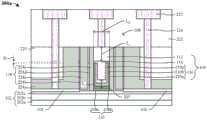
参照图1,包括具有栅极结构109的晶体管108的半导体器件100的一些实施例的剖视图。Referring to FIG. 1 , a cross-sectional view of some embodiments of a
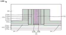
晶体管108上覆在衬底102上且包括栅极结构109、高介电常数栅极介电结构120、侧壁间隔件118以及源极/漏极区104。栅极结构109上覆在高介电常数栅极介电结构120上。侧壁间隔件118环绕栅极结构109及高介电常数栅极介电结构120。源极/漏极区104设置在晶体管108的相对侧上的衬底102内。选择性导电沟道106位于衬底102中、在横向上位于源极/漏极区104之间。在一些实施例中,源极/漏极区104及选择性导电沟道106是具有相反的掺杂类型的衬底102的掺杂区。举例来说,选择性导电沟道106可为p型且源极/漏极区104可为n型,或者选择性导电沟道106可为n型且源极/漏极区104可为p型。在一些实施例中,晶体管108可被配置成高介电常数金属栅极(HKMG)金属氧化物半导体场效应晶体管(MOSFET)。
层间介电(ILD)结构122上覆在晶体管108上。多个导通孔124延伸穿过ILD结构122。导通孔124上覆在栅极结构109及源极/漏极区104上。高介电常数栅极介电结构120包括具有一种或多种高介电常数介电材料的一个或多个介电层。本文所述的高介电常数介电材料是介电常数大于3.9的介电材料。栅极结构109包括硅化物层112、位于硅化物层112之下的栅极本体层114以及包绕在硅化物层112及栅极本体层114周围的功函数结构116(在一些实施例中,被称为金属层堆叠)。在一些实施例中,栅极本体层114是多晶硅层。功函数结构116可例如包括一个或多个金属层。An interlayer dielectric (ILD)
在一些实施例中,硅化物层112的外侧壁与栅极本体层114的外侧壁对齐。另外,硅化物层112的外侧壁及栅极本体层114的外侧壁直接接触功函数结构116的内侧壁。硅化物层112的顶表面与功函数结构116的顶表面实质上对齐。In some embodiments, outer sidewalls of the
通过在硅化物层112的外侧壁周围包绕功函数结构116且使硅化物层112的顶表面与功函数结构116的顶表面对齐,可简化晶体管108的制作。举例来说,硅化物层112的形成及功函数结构116的形成可包括单个平坦化工艺(例如,单个化学机械平坦化(CMP)工艺)。通过简化晶体管108的制作,可减少与半导体器件100的形成相关联的成本及时间。By wrapping the
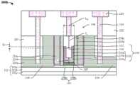
参照图2,提供根据图1所示半导体器件100的一些替代实施例的半导体器件200的剖视图。高介电常数栅极介电结构120包括介电层堆叠208a到208b,且功函数结构116包括金属层堆叠210a到210c。Referring to FIG. 2 , a cross-sectional view of a
在一些实施例中,衬底102可例如具有第一掺杂类型(例如,p型)。在一些实施例中,衬底102可例如为块状衬底(例如,块状硅衬底)、绝缘体上硅(silicon-on-insulator,SOI)衬底或一些其他合适的衬底。举例来说,衬底102可包括器件层202c、位于器件层202c之下的绝缘体层202b以及位于绝缘体层202b之下的处置衬底202a。在前述实例中,衬底102被配置成SOI衬底。器件层202c可例如为或可包含硅(例如(举例来说)单晶硅、非晶硅、块状硅等)。此外,器件层202c可例如具有第一掺杂类型。绝缘体层202b可例如为氧化物(例如氧化硅)。处置衬底202a可例如为或可包含硅(例如单晶硅、非晶硅、块状硅等)。In some embodiments,
源极/漏极区104是上覆在衬底102上的外延层。源极/漏极区104具有与第一掺杂类型相反的第二掺杂类型(例如,n型)。源极/漏极区104具有设置在衬底102的顶表面上方的顶表面,且具有设置在衬底102的顶表面下方的底表面。在一些实施例中,源极/漏极区104可为包括第二掺杂类型的器件层202c的离子注入区。在另一些实施例中,硅化物层(未示出)可设置在源极/漏极区104与上覆的导通孔124之间。在又一些实施例中,轻掺杂区(例如,掺杂浓度小于源极/漏极区)(未示出)在横向上设置在高介电常数栅极介电结构120与相应源极/漏极区104之间。轻掺杂区可例如为外延层和/或包括第二掺杂类型的器件层202c的分立掺杂区。在一些实施例中,隔离结构可在源极/漏极区104的最外区处设置在衬底102中以将晶体管108与衬底102上的相邻器件(未示出)电隔离。The source/
高介电常数栅极介电结构120包括介电层堆叠208a到208b。介电层堆叠208a到208b可分别例如为或可包含高介电常数介电材料(例如氮氧化硅、氧化铪、氮氧化铪、氧化铪铝、氧化锆等)。本文所述的高介电常数介电材料是介电常数大于3.9的介电材料。在一些实施例中,介电层堆叠208a到208b可分别为或可包含彼此不同的介电材料。在一些实施例中,第一栅极介电层208a上覆在衬底102上,且第二栅极介电层208b上覆在第一栅极介电层208a上。The high-k gate
功函数结构116包括金属层堆叠210a到210c。金属层堆叠210a到210c可分别例如为或可包含金属材料(例如钛、氮化钛、钛铝等)。在一些实施例中,金属层堆叠210a到210c可分别为或可包含彼此不同的金属材料。举例来说,第一金属层210a可为或可包含钛,第二金属层210b可为或可包含氮化钛,和/或第三金属层210c可为或可包含钛铝。功函数结构116具有在高介电常数栅极介电结构120的顶表面与栅极本体层114的底表面之间界定的垂直厚度Tv。在一些实施例中,垂直厚度Tv可处于近似4纳米到40纳米范围内。在一些实施例中,如果垂直厚度Tv大于4纳米,则可降低栅极结构109的电阻,同时维持栅极结构109的结构完整性。在另一些实施例中,如果垂直厚度Tv小于40纳米,则可降低栅极结构109的电阻,同时降低与功函数结构116的形成相关联的成本。在另一些实施例中,在功函数结构116与高介电常数栅极介电结构120之间设置有中间金属层207。在一些实施例中,中间金属层207是功函数结构116的一部分。在这种实施例中,中间金属层207可例如为或可包含金属材料(例如钛、氮化钛、钛铝等),和/或具有处于1纳米到10纳米范围内的厚度。在一些实施例中,栅极结构109的电阻降低可例如降低衬底和/或射频(radio frequency,RF)损耗。
在其中源极/漏极区104是n型的一些实施例中,栅极本体层114是n型多晶硅,功函数结构116包含具有n型功函数的金属或者具有n型功函数的一些其他合适的导电材料。本文所述具有n型功函数的金属可为或可包含例如铪、锆、钛、钽、铝、一些其他合适的n型功函数金属或前述金属的任意组合。在其中源极/漏极区104是p型的一些实施例中,栅极本体层114是p型多晶硅,功函数结构116包含具有p型功函数的金属或者具有p型功函数的一些其他合适的导电材料。本文所述具有p型功函数的金属可为例如钌、钯、铂、钴、镍、氮化钛铝、氮化钨碳、一些其他合适的p型功函数金属或前述金属的任意组合。In some embodiments in which the source/
在一些实施例中,金属层堆叠210a到210c分别可具有彼此不同的厚度。举例来说,第一金属层210a可具有比第二金属层210b的厚度小的厚度。第三金属层210c可具有比第二金属层210b的厚度小且比第一金属层210a的厚度大的厚度。金属层堆叠210a到210c中的每一金属层可分别具有处于约1纳米到10纳米范围内的厚度。功函数结构116具有U形,以使每一金属层210a到210c分别具有U形。在又一些实施例中,中间金属层207可具有比第三金属层210c小的厚度。In some embodiments, the metal layer stacks 210 a - 210 c may have different thicknesses from each other. For example, the
栅极本体层114设置在U形功函数结构116的中心内。因此,功函数结构116包绕在栅极本体层114的侧壁周围且以杯状包围栅极本体层114的下侧。栅极本体层114可例如为或可包含多晶硅。在前述实例中,可对多晶硅进行掺杂以使栅极本体层114与功函数结构116及硅化物层112形成欧姆接触(ohmic contact)。举例来说,栅极本体层114可包括掺杂浓度大于1*1019原子/cm3的第二掺杂类型(例如,n型)。掺杂多晶硅可例如降低栅极结构109的栅极电阻,从而降低晶体管108的功耗。在另一些实施例中,栅极本体层114可例如为或可包含本征(即,未掺杂)多晶硅。硅化物层112可例如为或可包含硅化镍、硅化钴、硅化钛、硅化铜等。在一些实施例中,栅极本体层114的厚度可为硅化物层112的厚度的四倍或更多倍。硅化物层112被配置成将上覆的导通孔124电耦合到功函数结构116。在一些实施例中,硅化物层112的外侧壁与栅极本体层114的外侧壁对齐。在一些实施例中,硅化物层112的厚度比垂直厚度Tv小。The
侧壁间隔件118包括多个间隔件介电层224b到224e。接触刻蚀停止层(contactetch stop layer,CESL)224a环绕第一间隔件介电间隔件层224b。在一些实施例中,CESL224a、第二间隔件介电层224c与第四间隔件介电层224e可分别为或可包含相同的介电材料。所述相同的介电材料可例如为或可包含氮化硅、碳化硅等。CESL 224a具有处于约10纳米到20纳米范围内的第一介电厚度T1d。第二间隔件介电层224c具有处于约10纳米到30纳米范围内的第三介电厚度T3d。第四间隔件介电层224e具有处于约3纳米到5纳米范围内的第五介电厚度T5d。在一些实施例中,第一间隔件介电层224b与第三间隔件介电层224d可分别为或可包含另一种相同的介电材料。所述另一种相同的介电材料可例如为或可包含氧化物(例如氧化硅等)。在另一些实施例中,第一间隔件介电层224b及第三间隔件介电层224d是具有U形的单个连续介电层。所述单个连续介电层可包绕在第二间隔件介电层224c的侧壁周围且以杯状包围第二间隔件介电层224c的下侧。The sidewall spacers 118 include a plurality of spacer
第一ILD层220上覆在CESL 224a上。第二ILD层222上覆在晶体管108及第一ILD层220上。导通孔124从导电线223延伸穿过第二ILD层222以将硅化物层112及源极/漏极区104电耦合到上覆的金属层(例如,上覆的内连结构中的导电层)和/或其他半导体器件(例如,存储单元)(未示出)。在一些实施例中,第一ILD层220及第二ILD层222可例如分别为或可包含低介电常数介电材料、氧化硅等。本文所述低介电常数介电材料是介电常数小于3.9的介电材料。导通孔124可例如分别为或可包含铝、铜等。导电线223可例如分别为或可包含铝铜等。The
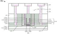
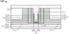
参照图3A,提供根据图2所示半导体器件200的一些替代实施例的半导体器件300a的剖视图,其中栅极本体层114具有T形。Referring to FIG. 3A , there is provided a cross-sectional view of a
栅极本体层114具有T形以使栅极本体层114的顶表面在垂直方向上位于功函数结构116的顶表面上方距离d1。在一些实施例中,距离d1可处于约1纳米到10纳米范围内。因此,功函数结构116包绕在栅极本体层114的外侧壁周围且以杯状包围栅极本体层114的下侧。栅极本体层114的上部部分悬垂于功函数结构116上。硅化物层112的外侧壁与功函数结构116的外侧壁对齐。硅化物层112的厚度Ts大于功函数结构116的厚度Tv。The
在一些实施例中,硅化物层112的厚度Ts处于约5纳米到30纳米范围内。在一些实施例中,如果厚度Ts大于5纳米,则栅极结构109的栅极电阻减小。在另一些实施例中,如果厚度Ts小于30纳米,则栅极结构109的栅极电阻减小,同时减轻在用于形成硅化物层112的硅化物工艺期间对半导体器件300a的结构的损坏。使硅化物层112的外侧壁与功函数结构116的外侧壁对齐有利于减小栅极结构109的长度Lg。由于硅化物层112的轮廓,长度Lg可减小到小于26纳米,从而提高使晶体管108按比例缩放的能力和/或增加设置在单个硅晶片上的晶体管108的数目。In some embodiments, the thickness Ts of the
参照图3B,提供根据图2所示半导体器件200的一些替代实施例的半导体器件300b的剖视图。硅化物层112的底表面比功函数结构116的顶表面低距离d2。在一些实施例中,距离d2可处于约1纳米到10纳米范围内。硅化物层112具有T形。因此,功函数结构116包绕在硅化物层112的突起部的外侧壁周围。Referring to FIG. 3B , a cross-sectional view of a
参照图3C,提供根据图2所示半导体器件200的一些替代实施例的半导体器件300c的剖视图。栅极本体层114从侧壁间隔件118的上表面延伸到功函数结构116的上表面。栅极本体层114具有相对于功函数结构116的顶表面在垂直方向上偏置的顶表面,且还具有被功函数结构116以杯状包围的向下突起部。在一些实施例中,栅极本体层114是单种材料。所述单种材料可例如为或可包含铝或一些其他合适的材料。Referring to FIG. 3C , a cross-sectional view of a
图4到图9示出根据本公开各个方面的形成包括具有硅化物层的高介电常数金属栅极(HKMG)结构的半导体器件的第一方法的一些实施例的剖视图400到900。尽管参照一种方法阐述图4到图9中所示剖视图400到900,然而应理解,图4到图9中所示的结构不限于所述方法,而是可独立于所述方法。此外,尽管图4到图9被阐述为一系列动作,然而应理解,这些动作不是限制性的,所述动作的次序可在其他实施例中进行更改,且所公开的方法也适用于其他结构。在其他实施例中,可整体地或部分地省略所示和/或所阐述的一些动作。在一些实施例中,可例如采用图4到图9以形成图2所示半导体器件200。4-9 illustrate cross-sectional views 400-900 of some embodiments of a first method of forming a semiconductor device including a high-k metal gate (HKMG) structure having a silicide layer according to various aspects of the present disclosure. Although the cross-sectional views 400-900 shown in FIGS. 4-9 are described with reference to a method, it should be understood that the structures shown in FIGS. 4-9 are not limited to the method but may be independent of the method. Additionally, while FIGS. 4-9 are illustrated as a series of acts, it should be understood that these acts are not limiting, that the order of the acts may be altered in other embodiments, and that the disclosed methods are applicable to other structures as well. . In other embodiments, some actions shown and/or described may be omitted in whole or in part. In some embodiments, the
如图4所示剖视图400所示,提供上覆在衬底102上的虚设栅极电极结构402。在一些实施例中,用于形成图4所示结构的方法可包括在衬底102之上形成高介电常数栅极介电结构120。虚设栅极电极结构402形成在高介电常数栅极介电结构120之上。在形成虚设栅极电极结构402之后,可在衬底102之上外延形成源极/漏极区104。在替代实施例中,源极/漏极区104可通过掺杂工艺形成在衬底102中。可在虚设栅极电极结构402及高介电常数栅极介电结构120周围形成侧壁间隔件118。可在侧壁间隔件118周围形成接触刻蚀停止层(CESL)224a。在侧壁间隔件118、虚设栅极电极结构402及CESL 224a之上形成第一层间介电(ILD)层220。As shown in the
如图5所示剖视图500所示,移除虚设栅极电极结构(图4所示402),从而在高介电常数栅极介电结构120上方界定开口502。在一些实施例中,在移除虚设栅极电极结构(图4所示402)之前,对第一ILD层220执行平坦化工艺(例如,化学机械平坦化(CMP)工艺)。执行平坦化工艺直到暴露出侧壁间隔件118的上表面及虚设栅极电极结构(图4所示402)的上表面。虚设栅极电极结构(图4所示402)可通过以下步骤移除:在图4所示结构之上形成掩蔽层(未示出);根据掩蔽层执行刻蚀工艺,从而界定开口502;以及随后移除掩蔽层。As shown in the
如图6所示剖视图600所示,在图5所示结构之上形成功函数结构116、中间金属层207及栅极本体层114。功函数结构116对开口(图5所示502)进行衬垫。栅极本体层114包括突出到开口(图5所示502)中且被功函数结构116以杯状包围的突起部。功函数结构116及中间金属层207具有界定在高介电常数栅极介电结构120的顶表面与栅极本体层114的底表面之间的垂直厚度Tv。在一些实施例中,垂直厚度Tv可处于近似4纳米到40纳米范围内。在一些实施例中,栅极本体层114可例如为或可包含单种材料(例如多晶硅)。在前述实施例中,多晶硅可掺杂有第二掺杂类型(例如,n型)。在一些实施例中,可对栅极本体层114执行离子注入工艺以将第二掺杂类型注入到多晶硅中。As shown in the
如图7所示剖视图700所示,执行硅化物工艺以将栅极本体层114的一部分转换成硅化物层112。在一些实施例中,硅化物工艺包括在图6所示结构之上形成导电层(未示出)以及随后执行退火工艺(annealing process)以将导电层及栅极本体层114的所述部分转换成硅化物层112。硅化物层112的底表面在侧壁间隔件118的顶表面下方延伸。As shown in the
如图8所示剖视图800所示,对图7所示结构执行平坦化工艺(例如,CMP工艺)直到达到侧壁间隔件118的上表面。这在高介电常数栅极介电结构120之上部分地界定栅极结构109,且进一步部分地界定了包括栅极结构109的晶体管108。因此,在一些实施例中,晶体管108可通过使用两个平坦化工艺来形成。这部分地减少了与形成晶体管108相关联的制作成本及时间。As shown in the
如图9所示剖视图900所示,在第一ILD层220之上形成第二ILD层222。在源极/漏极区104及硅化物层112之上形成导通孔124及导电线223。As shown in the
图10示出根据本公开的形成包括具有硅化物层的高介电常数金属栅极(HKMG)结构的半导体器件的方法1000。尽管方法1000被示出和/或阐述为一系列动作或事件,然而应理解,所述方法不限于所示次序或动作。因此,在一些实施例中,可以与所示次序不同的次序施行所述动作和/或可同时施行所述动作。此外,在一些实施例中,可将所示动作或事件细分成多个动作或事件,所述多个动作或事件可分次单独施行或与其他动作或子动作同时施行。在一些实施例中,可省略一些所示动作或事件,且可包括其他未示出的动作或事件。在一些实施例中,方法1000涉及图4到图9所示第一方法。FIG. 10 illustrates a
在动作1002处,在衬底之上形成高介电常数栅极介电结构且在高介电常数栅极介电结构之上形成虚设栅极电极结构。图4示出与动作1002的一些实施例对应的剖视图400。At
在动作1004处,在虚设栅极电极结构及高介电常数栅极介电结构周围形成侧壁间隔件。图4示出与动作1004的一些实施例对应的剖视图400。At
在动作1006处,移除虚设栅极电极结构,从而在侧壁间隔件的上表面与高介电常数栅极介电结构的上表面之间形成开口。图5示出与动作1006的一些实施例对应的剖视图500。At
在动作1008处,在开口中以及侧壁间隔件之上形成功函数结构及栅极本体层。图6示出与动作1008的一些实施例对应的剖视图600。At
在动作1010处,将栅极本体层的上部部分转换成硅化物层。图7示出与动作1010的一些实施例对应的剖视图700。At
在动作1012处,对功函数结构及硅化物层执行平坦化工艺直到暴露出侧壁间隔件的上表面,从而界定栅极电极结构。图8示出与动作1012的一些实施例对应的剖视图800。At
图11到图18示出根据本公开各个方面的形成包括高介电常数金属栅极(HKMG)结构的半导体器件的第二方法的一些实施例的剖视图1100到1800。尽管参照一种方法阐述了图11到图18中所示剖视图1100到1800,然而应理解,图11到图18中所示的结构不限于所述方法,而是可独立于所述方法。此外,尽管图11到图18被阐述为一系列动作,然而应理解,这些动作不是限制性的,所述动作的次序可在其他实施例中进行更改,且所公开的方法也适用于其他结构。在其他实施例中,可整体地或部分地省略所示和/或所阐述的一些动作。在一些实施例中,可例如采用图11到图18以形成图3A所示半导体器件300a。11 to 18 illustrate
如图11所示剖视图1100所示,提供上覆在衬底102上的虚设栅极电极结构1102。在一些实施例中,用于形成图11所示结构的方法可包括在衬底102之上形成高介电常数栅极介电结构120。虚设栅极电极结构1102形成在高介电常数栅极介电结构120之上。在形成虚设栅极电极结构1102之后,可在衬底102之上外延形成源极/漏极区104。在替代实施例中,源极/漏极区104可通过掺杂工艺形成在衬底102中。可在虚设栅极电极结构1102及高介电常数栅极介电结构120周围形成侧壁间隔件118。可在侧壁间隔件118周围形成接触刻蚀停止层(CESL)224a。在侧壁间隔件118、虚设栅极电极结构1102及CESL 224a之上形成第一层间介电(ILD)层220。As shown in the
如图12所示剖视图1200所示,移除虚设栅极电极结构(图11所示1102),从而在高介电常数栅极介电结构120上方界定第一开口1202。在一些实施例中,在移除虚设栅极电极结构(图11所示1102)之前,对第一ILD层220执行平坦化工艺(例如,CMP工艺)。执行平坦化工艺直到暴露出侧壁间隔件118的上表面及虚设栅极电极结构(图11所示1102)的上表面。虚设栅极电极结构(图11所示1102)可通过以下步骤移除:在图11所示结构之上形成掩蔽层(未示出);根据掩蔽层执行刻蚀工艺,从而界定第一开口1202;以及随后移除掩蔽层。As shown in the
如图13所示剖视图1300所示,在图12所示结构之上形成功函数结构116及中间金属层207。功函数结构116对第一开口1202的一部分进行衬垫并直接接触侧壁间隔件118的内侧壁。功函数结构116及中间金属层207具有界定在高介电常数栅极介电结构120的顶表面与功函数结构116的上表面之间的垂直厚度Tv。在一些实施例中,垂直厚度Tv可处于近似4纳米到40纳米范围内。As shown in the
如图14所示剖视图1400所示,对功函数结构116执行刻蚀工艺,从而暴露出侧壁间隔件118的内侧壁的一部分。功函数结构116的顶表面被设置成低于侧壁间隔件118的上表面。As shown in the
如图15所示剖视图1500所示,在侧壁间隔件118及功函数结构116之上形成栅极本体层114,从而填充第一开口(图12所示1202)。在一些实施例中,栅极本体层114可例如为或可包含单种材料(例如多晶硅)。在前述实施例中,多晶硅可掺杂有第二掺杂类型(例如,n型)。在一些实施例中,可对栅极本体层114执行离子注入工艺以将第二掺杂类型注入到多晶硅中。As shown in the
如图16所示剖视图1600所示,对图15所示结构执行平坦化工艺(例如,CMP工艺)。在一些实施例中,对栅极本体层114执行平坦化工艺直到暴露出侧壁间隔件118的上表面。As shown in
如图17所示剖视图1700所示,对图16所示结构执行硅化物工艺以将栅极本体层114的一部分转换成硅化物层112,从而界定栅极结构109。在一些实施例中,硅化物工艺包括在图16所示结构之上形成导电层(未示出)以及随后执行退火工艺以将导电层及栅极本体层114的所述部分转换成硅化物层112。栅极本体层114具有T形以使栅极本体层114的顶表面在垂直方向上位于功函数结构116的顶表面上方距离d1。在一些实施例中,距离d1可处于约1纳米到10纳米范围内。在替代实施例中,栅极本体层114的顶表面在垂直方向上位于功函数结构116(参见例如图3B)的顶表面下方。硅化物层112的厚度Ts比功函数结构116的厚度Tv大。在一些实施例中,执行硅化物工艺以使硅化物层112的厚度Ts处于约5纳米到30纳米范围内。As shown in the
如图18所示剖视图1800所示,在第一ILD层220之上形成第二ILD层222。在源极/漏极区104及硅化物层112之上形成导通孔124及导电线223。As shown in the
在一些实施例中,可更改图11到图18所示第二方法以形成图3C所示半导体器件300c。举例来说,在图15处,可形成栅极本体层114以使栅极本体层114是单种材料且为或包含铝或一些其他合适的金属。在前述实例中,可省略在图17处执行的硅化物工艺,以使在执行图16所示平坦化工艺之后界定栅极结构109。通过简化栅极结构109的制作,可减少与图3C所示半导体器件300c的形成相关联的成本及时间。在一些实施例中,以使栅极本体层114的外侧壁与功函数结构116的外侧壁对齐的方式形成栅极本体层114。这部分地有利于在功函数结构116的内侧壁周围以及功函数结构116的顶表面之上形成栅极本体层114。由于栅极本体层的轮廓,栅极结构109的长度Lg可减小到例如小于26纳米。In some embodiments, the second method shown in FIGS. 11 to 18 may be modified to form the
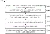
图19示出根据本公开的形成包括高介电常数金属栅极(HKMG)结构的半导体器件的方法1900。尽管方法1900被示出和/或阐述为一系列动作或事件,然而应理解,所述方法不限于所示次序或动作。因此,在一些实施例中,可以与所示次序不同的次序施行所述动作和/或可同时施行所述动作。此外,在一些实施例中,可将所示动作或事件细分成多个动作或事件,所述多个动作或事件可分次单独施行或与其他动作或子动作同时施行。在一些实施例中,可省略一些所示动作或事件,且可包括其他未示出的动作或事件。在一些实施例中,方法1900涉及图11到图18所示第二方法。FIG. 19 illustrates a
在动作1902处,在衬底之上形成高介电常数栅极介电结构,且在高介电常数栅极介电结构之上形成虚设栅极电极结构。图11示出与动作1902的一些实施例对应的剖视图1100。At
在动作1904处,在虚设栅极电极结构及高介电常数栅极介电结构周围形成侧壁间隔件。图11示出与动作1904的一些实施例对应的剖视图1100。At
在动作1906处,移除虚设栅极电极结构,从而在侧壁间隔件的上表面与高介电常数栅极介电结构的上表面之间形成开口。图12示出与动作1906的一些实施例对应的剖视图1200。At
在动作1908处,在开口中以及侧壁间隔件之上形成功函数结构。图13示出与动作1908的一些实施例对应的剖视图1300。At
在动作1910处,执行刻蚀工艺以移除功函数结构的一部分以使功函数结构的顶表面低于侧壁间隔件的顶表面。图14示出与动作1910的一些实施例对应的剖视图1400。At
在动作1912处,在功函数结构及侧壁间隔件之上形成栅极本体层以使功函数结构以杯状包围栅极本体层的下部部分的下侧。图15示出与动作1912的一些实施例对应的剖视图1500。At
在动作1914处,对栅极本体层执行平坦化工艺直到暴露出侧壁间隔件的上表面。图16示出与动作1914的一些实施例对应的剖视图1600。At
在动作1916处,将栅极本体层的上部部分转换成硅化物层。图17示出与动作1916的一些实施例对应的剖视图1700。At
因此,在一些实施例中,本申请提供一种用于使用两个平坦化工艺形成晶体管的方法,所述晶体管包括栅极结构,所述栅极结构包括硅化物层及被功函数结构环绕的栅极本体层。在另一些实施例中,本申请提供一种晶体管,所述晶体管包括栅极结构,所述栅极结构包括栅极本体层及功函数结构。栅极本体层具有相对于功函数结构的顶表面在垂直方向上偏置的顶表面且还具有被功函数结构以杯状包围的下部部分。Accordingly, in some embodiments, the present application provides a method for forming a transistor using two planarization processes, the transistor including a gate structure including a silicide layer and a gate structure surrounded by a work function structure. Gate body layer. In some other embodiments, the present application provides a transistor, the transistor includes a gate structure, and the gate structure includes a gate body layer and a work function structure. The gate body layer has a top surface that is offset in a vertical direction with respect to the top surface of the work function structure and also has a lower portion surrounded by the work function structure in a cup shape.
在一些实施例中,本申请提供一种半导体器件,所述半导体器件包括:一对间隔件段,位于半导体衬底上;高介电常数栅极介电结构,上覆在所述半导体衬底上,其中所述高介电常数栅极介电结构在横向上位于所述间隔件段之间且与所述间隔件段相邻;以及栅极结构,位于所述高介电常数栅极介电结构之上且具有与所述间隔件段的顶表面大约齐平的顶表面,其中所述栅极结构包括金属结构及栅极本体层,其中所述栅极本体层具有相对于所述金属结构的顶表面在垂直方向上偏置的顶表面且还具有被所述金属结构以杯状包围的下部部分。In some embodiments, the present application provides a semiconductor device comprising: a pair of spacer segments on a semiconductor substrate; a high-k gate dielectric structure overlying the semiconductor substrate wherein the high-k gate dielectric structure is laterally located between and adjacent to the spacer segments; and a gate structure located between the high-k gate dielectric structures and having a top surface approximately flush with the top surface of the spacer segment, wherein the gate structure includes a metal structure and a gate body layer, wherein the gate body layer has a The top surface is vertically offset and also has a lower portion cupped by the metal structure.
在一些实施例中,所述栅极本体层是T形的且所述金属结构是U形的。在一些实施例中,所述栅极结构还包括:硅化物层,上覆在所述栅极本体层上,其中所述硅化物层界定所述栅极结构的所述顶表面;其中所述栅极本体层包含多晶硅。在一些实施例中,所述硅化物层具有T形轮廓且从所述栅极结构的所述顶表面连续地延伸到位于所述金属结构的所述顶表面下方的点。在一些实施例中,所述硅化物层的底表面位于所述金属结构的所述顶表面上方且通过所述栅极本体层而与所述金属结构隔开。在一些实施例中,所述多晶硅是本征多晶硅。在一些实施例中,所述栅极本体层包含单种材料,且其中所述单种材料是铝。在一些实施例中,所述栅极本体层的最外侧壁与所述金属结构的最外侧壁对齐,且所述栅极本体层的所述下部部分的侧壁直接接触所述金属结构的内侧壁。In some embodiments, the gate body layer is T-shaped and the metal structure is U-shaped. In some embodiments, the gate structure further includes: a silicide layer overlying the gate body layer, wherein the silicide layer defines the top surface of the gate structure; wherein the The gate body layer includes polysilicon. In some embodiments, the silicide layer has a T-shaped profile and extends continuously from the top surface of the gate structure to a point below the top surface of the metal structure. In some embodiments, a bottom surface of the silicide layer is above the top surface of the metal structure and is separated from the metal structure by the gate body layer. In some embodiments, the polysilicon is intrinsic polysilicon. In some embodiments, the gate body layer includes a single material, and wherein the single material is aluminum. In some embodiments, the outermost sidewall of the gate body layer is aligned with the outermost sidewall of the metal structure, and the sidewall of the lower portion of the gate body layer directly contacts the inner side of the metal structure. wall.
在一些实施例中,本申请提供一种半导体器件,所述半导体器件包括:一对源极/漏极区,位于半导体衬底中;高介电常数栅极介电结构,上覆在所述半导体衬底上,其中所述高介电常数栅极介电结构在横向上位于所述源极/漏极区之间且与所述源极/漏极区相邻;以及栅极结构,上覆在所述高介电常数栅极介电结构上,其中所述栅极结构包括堆叠在一起的栅极本体层与硅化物层,其中所述栅极结构还包括功函数结构,所述功函数结构包绕在所述栅极本体层的底部周围且沿着所述栅极本体层的侧壁及所述硅化物层的侧壁延伸到所述功函数结构的顶表面,且其中所述功函数结构的所述顶表面与所述硅化物层的顶表面大约齐平。In some embodiments, the present application provides a semiconductor device, which includes: a pair of source/drain regions located in a semiconductor substrate; a high dielectric constant gate dielectric structure overlying the On a semiconductor substrate, wherein the high-k gate dielectric structure is laterally located between and adjacent to the source/drain regions; and a gate structure, on overlying on the high dielectric constant gate dielectric structure, wherein the gate structure includes a gate body layer and a silicide layer stacked together, wherein the gate structure further includes a work function structure, and the work function The function structure is wrapped around the bottom of the gate body layer and extends along the sidewalls of the gate body layer and the sidewalls of the silicide layer to the top surface of the work function structure, and wherein the The top surface of the work function structure is approximately level with the top surface of the suicide layer.
在一些实施例中,所述栅极本体层的最外侧壁与所述硅化物层的最外侧壁对齐。在一些实施例中,所述栅极本体层的所述最外侧壁及所述硅化物层的所述最外侧壁直接接触所述功函数结构的内侧壁。在一些实施例中,所述栅极本体层的厚度比所述硅化物层的厚度大三倍或更多倍。在一些实施例中,所述功函数结构是U形的。在一些实施例中,半导体器件还包括:侧壁间隔件,环绕所述高介电常数栅极介电结构的侧壁及所述栅极结构的侧壁,其中所述侧壁间隔件的顶表面与所述硅化物层的顶表面实质上对齐。在一些实施例中,所述栅极本体层包含本征多晶硅。在一些实施例中,所述功函数结构包括三个U形金属层。在一些实施例中,所述三个U形金属层各自包含彼此不同的金属材料。In some embodiments, the outermost sidewall of the gate body layer is aligned with the outermost sidewall of the silicide layer. In some embodiments, the outermost sidewall of the gate body layer and the outermost sidewall of the silicide layer directly contact the inner sidewall of the work function structure. In some embodiments, the thickness of the gate body layer is three or more times greater than the thickness of the silicide layer. In some embodiments, the work function structure is U-shaped. In some embodiments, the semiconductor device further includes: a sidewall spacer surrounding the sidewall of the high-k gate dielectric structure and the sidewall of the gate structure, wherein the top of the sidewall spacer A surface is substantially aligned with a top surface of the suicide layer. In some embodiments, the gate body layer includes intrinsic polysilicon. In some embodiments, the work function structure includes three U-shaped metal layers. In some embodiments, the three U-shaped metal layers each comprise different metal materials from each other.
在一些实施例中,本申请提供一种制造半导体器件的方法,所述方法包括:在半导体衬底之上形成虚设栅极结构,其中所述虚设栅极结构包括上覆在所述半导体衬底上的高介电常数栅极介电结构且还包括上覆在所述高介电常数栅极介电结构上的虚设栅极电极,且其中侧壁间隔件环绕所述虚设栅极结构;使用栅极电极层堆叠置换所述虚设栅极电极,其中所述栅极电极层堆叠包括金属层及上覆在所述金属层上的多晶硅层;将所述多晶硅层的上部部分转换成硅化物层;以及对所述栅极电极层堆叠及所述硅化物层执行平坦化工艺直到暴露出所述侧壁间隔件的上表面,从而界定栅极电极结构,其中所述平坦化工艺局部地移除所述硅化物层。In some embodiments, the present application provides a method of manufacturing a semiconductor device, the method comprising: forming a dummy gate structure over a semiconductor substrate, wherein the dummy gate structure includes and further comprising a dummy gate electrode overlying the high-k gate dielectric structure, and wherein sidewall spacers surround the dummy gate structure; using a gate electrode layer stack replacing the dummy gate electrode, wherein the gate electrode layer stack includes a metal layer and a polysilicon layer overlying the metal layer; converting an upper portion of the polysilicon layer into a silicide layer and performing a planarization process on the gate electrode layer stack and the silicide layer until upper surfaces of the sidewall spacers are exposed, thereby defining a gate electrode structure, wherein the planarization process locally removes The silicide layer.
在一些实施例中,所述平坦化工艺包括对所述硅化物层及所述金属层执行化学机械平坦化工艺直到暴露出所述侧壁间隔件的所述上表面,且其中所述化学机械平坦化工艺不到达所述多晶硅层。在一些实施例中,将所述多晶硅层的所述上部部分转换成硅化物层包括:在形成所述栅极电极层堆叠之后,在所述多晶硅层之上形成导电层;以及对所述导电层及所述多晶硅层执行退火工艺,从而界定所述硅化物层,其中所述硅化物层具有在所述金属层的顶表面下方延伸的向下突起部。In some embodiments, the planarization process includes performing a chemical mechanical planarization process on the silicide layer and the metal layer until the upper surface of the sidewall spacer is exposed, and wherein the chemical mechanical The planarization process does not reach the polysilicon layer. In some embodiments, converting the upper portion of the polysilicon layer into a silicide layer includes: forming a conductive layer over the polysilicon layer after forming the gate electrode layer stack; layer and the polysilicon layer are annealed to define the silicide layer, wherein the silicide layer has a downward protrusion extending below the top surface of the metal layer.
在一些实施例中,本申请提供一种制造半导体器件的方法,所述方法包括:在半导体衬底之上形成虚设栅极结构,其中所述虚设栅极结构包括上覆在所述半导体衬底上的高介电常数栅极介电结构且还包括位于所述高介电常数栅极介电结构之上的虚设栅极电极,且其中侧壁间隔件环绕所述虚设栅极结构;使用金属层堆叠置换所述虚设栅极电极,以使所述金属层堆叠上覆在所述高介电常数栅极介电结构及所述侧壁间隔件上;执行刻蚀工艺以移除上覆在所述侧壁间隔件上的所述金属层堆叠的一部分且使所述金属层堆叠的顶表面凹陷到低于所述侧壁间隔件的顶表面;以及在所述金属层堆叠之上形成栅极本体,其中所述栅极本体的下部部分被所述金属层堆叠环绕且所述栅极本体的上部部分悬垂于所述金属层堆叠上。在一些实施例中,其中所述形成所述栅极本体包括:在所述金属层堆叠及所述侧壁间隔件之上形成多晶硅层,其中所述多晶硅层具有被所述金属层堆叠环绕的下部部分;对所述多晶硅层执行平坦化工艺直到暴露出所述侧壁间隔件的所述顶表面;在所述多晶硅层之上形成导电层;以及对所述多晶硅层及所述导电层执行退火工艺,从而将所述多晶硅层的上部部分转换成硅化物层,其中所述硅化物层的外侧壁与所述金属层堆叠的外侧壁对齐。在一些实施例中,所述硅化物层从所述侧壁间隔件的所述顶表面连续地延伸到位于所述金属层堆叠的所述顶表面下方的点。在一些实施例中,所述硅化物层的底表面位于所述金属层堆叠的顶表面上方且所述硅化物层通过所述多晶硅层而与所述金属层堆叠隔开。在一些实施例中,所述形成所述栅极本体包括:在所述金属层堆叠及所述侧壁间隔件之上形成导电层,其中所述导电层包含单种材料;以及对所述导电层执行平坦化工艺直到暴露出所述侧壁间隔件的顶表面。在一些实施例中,所述单种材料是铝。In some embodiments, the present application provides a method of manufacturing a semiconductor device, the method comprising: forming a dummy gate structure over a semiconductor substrate, wherein the dummy gate structure includes and further comprising a dummy gate electrode over the high-k gate dielectric structure, and wherein sidewall spacers surround the dummy gate structure; using a metal layer stack displacing the dummy gate electrode such that the metal layer stack overlies the high-k gate dielectric structure and the sidewall spacers; an etch process is performed to remove the overlying a portion of the metal layer stack on the sidewall spacer and recess the top surface of the metal layer stack below the top surface of the sidewall spacer; and forming a gate over the metal layer stack A pole body, wherein a lower portion of the gate body is surrounded by the metal layer stack and an upper portion of the gate body overhangs the metal layer stack. In some embodiments, the forming the gate body includes: forming a polysilicon layer over the metal layer stack and the sidewall spacers, wherein the polysilicon layer has a metal layer surrounded by the metal layer stack. lower portion; performing a planarization process on the polysilicon layer until the top surfaces of the sidewall spacers are exposed; forming a conductive layer over the polysilicon layer; and performing a process on the polysilicon layer and the conductive layer an annealing process to convert the upper portion of the polysilicon layer into a silicide layer, wherein the outer sidewalls of the silicide layer are aligned with the outer sidewalls of the metal layer stack. In some embodiments, the silicide layer extends continuously from the top surface of the sidewall spacer to a point below the top surface of the metal layer stack. In some embodiments, the bottom surface of the silicide layer is above the top surface of the metal layer stack and the silicide layer is separated from the metal layer stack by the polysilicon layer. In some embodiments, the forming the gate body includes: forming a conductive layer over the metal layer stack and the sidewall spacers, wherein the conductive layer includes a single material; A planarization process is performed until the top surfaces of the sidewall spacers are exposed. In some embodiments, the single material is aluminum.
以上概述了若干实施例的特征,以使所属领域中的技术人员可更好地理解本公开的各个方面。所属领域中的技术人员应理解,他们可容易地使用本公开作为设计或修改其他工艺及结构的基础来施行与本文中所介绍的实施例相同的目的和/或实现与本文中所介绍的实施例相同的优点。所属领域中的技术人员还应认识到,这些等效构造并不背离本公开的精神及范围,而且他们可在不背离本公开的精神及范围的条件下对本文作出各种改变、代替及变更。The foregoing outlines features of several embodiments so that those skilled in the art may better understand the various aspects of the present disclosure. Those skilled in the art should appreciate that they may readily use this disclosure as a basis for designing or modifying other processes and structures to carry out the same purposes and/or implement the embodiments described herein. example with the same advantages. Those skilled in the art should also realize that such equivalent constructions do not depart from the spirit and scope of the present disclosure, and that they may make various changes, substitutions and alterations herein without departing from the spirit and scope of the present disclosure. .
[符号的说明][explanation of the symbol]
100、200、300a、300b、300c:半导体器件100, 200, 300a, 300b, 300c: Semiconductor devices
102:衬底102: Substrate
104:源极/漏极区104: source/drain region
106:选择性导电沟道106: Selective conduction channel
108:晶体管108: Transistor
109:栅极结构109: Gate structure
112:硅化物层112: Silicide layer
114:栅极本体层114: gate body layer
116:功函数结构116: Work function structure
118:侧壁间隔件118: Side wall spacer
120:高介电常数栅极介电结构120: High dielectric constant gate dielectric structure
122:层间介电(ILD)结构122: Interlayer Dielectric (ILD) Structure
124:导通孔124: via hole
202a:处置衬底202a: Disposing of the substrate
202b:绝缘体层202b: Insulator layer
202c:器件层202c: device layer
207:中间金属层207: middle metal layer
208a:介电层堆叠/第一栅极介电层208a: Dielectric layer stack/first gate dielectric layer
208b:介电层堆叠/第二栅极介电层208b: Dielectric layer stack/second gate dielectric layer
210a:金属层堆叠/第一金属层/金属层210a: Metal layer stack/first metal layer/metal layer
210b:金属层堆叠/第二金属层/金属层210b: metal layer stack/second metal layer/metal layer
210c:金属层堆叠/第三金属层/金属层210c: Metal Layer Stack/Third Metal Layer/Metal Layer
220:第一层间介电(ILD)层220: first interlayer dielectric (ILD) layer
222:第二层间介电(ILD)层222: Second interlayer dielectric (ILD) layer
223:导电线223: Conductive thread
224a:接触刻蚀停止层(CESL)224a: contact etch stop layer (CESL)
224b:间隔件介电层/第一间隔件介电间隔件层/第一间隔件介电层224b: spacer dielectric layer/first spacer dielectric spacer layer/first spacer dielectric layer
224c:间隔件介电层/第二间隔件介电层224c: spacer dielectric layer/second spacer dielectric layer
224d:间隔件介电层/第三间隔件介电层224d: spacer dielectric layer/third spacer dielectric layer
224e:间隔件介电层/第四间隔件介电层224e: spacer dielectric layer/fourth spacer dielectric layer
400、500、600、700、800、900、1100、1200、1300、1400、1500、1600、1700、1800:剖视图400, 500, 600, 700, 800, 900, 1100, 1200, 1300, 1400, 1500, 1600, 1700, 1800: cutaway view
402、1102:虚设栅极电极结构402, 1102: dummy gate electrode structure
502:开口502: opening
1000、1900:方法1000, 1900: method
1002、1004、1006、1008、1010、1012、1902、1904、1906、1908、1910、1912、1914、1916:动作1002, 1004, 1006, 1008, 1010, 1012, 1902, 1904, 1906, 1908, 1910, 1912, 1914, 1916: action
1202:第一开口1202: First opening
d1、d2:距离d1 , d2 : distance
Lg:长度Lg : length
T1d:第一介电厚度T1d : first dielectric thickness
T3d:第三介电厚度T3d : third dielectric thickness
T5d:第五介电厚度T5d : fifth dielectric thickness
Ts:厚度Ts : Thickness
Tv:垂直厚度/厚度。Tv : vertical thickness/thickness.
Claims (20)
Applications Claiming Priority (4)
| Application Number | Priority Date | Filing Date | Title |
|---|---|---|---|
| US201962799939P | 2019-02-01 | 2019-02-01 | |
| US62/799,939 | 2019-02-01 | ||
| US16/580,296 | 2019-09-24 | ||
| US16/580,296US11335786B2 (en) | 2019-02-01 | 2019-09-24 | Gate structure in high-κ metal gate technology |
Publications (2)
| Publication Number | Publication Date |
|---|---|
| CN111524974A CN111524974A (en) | 2020-08-11 |
| CN111524974Btrue CN111524974B (en) | 2023-06-02 |
Family
ID=71837958
Family Applications (1)
| Application Number | Title | Priority Date | Filing Date |
|---|---|---|---|
| CN202010054768.2AActiveCN111524974B (en) | 2019-02-01 | 2020-01-17 | Semiconductor device and manufacturing method thereof |
Country Status (3)
| Country | Link |
|---|---|
| US (3) | US11335786B2 (en) |
| CN (1) | CN111524974B (en) |
| TW (1) | TWI744774B (en) |
Families Citing this family (2)
| Publication number | Priority date | Publication date | Assignee | Title |
|---|---|---|---|---|
| US11362030B2 (en)* | 2020-05-29 | 2022-06-14 | Taiwan Semiconductor Manufacturing Company, Ltd. | Sidewall spacer structure enclosing conductive wire sidewalls to increase reliability |
| TWI809742B (en)* | 2021-12-03 | 2023-07-21 | 南亞科技股份有限公司 | Semiconductor device |
Citations (4)
| Publication number | Priority date | Publication date | Assignee | Title |
|---|---|---|---|---|
| CN102104061A (en)* | 2009-12-21 | 2011-06-22 | 台湾积体电路制造股份有限公司 | Gate electrodes for field effect transistors and field effect transistors |
| CN104377169A (en)* | 2013-08-13 | 2015-02-25 | 格罗方德半导体公司 | Fully silicided gate formed according to the gate-first hkmg approach |
| CN106935589A (en)* | 2015-12-30 | 2017-07-07 | 台湾积体电路制造股份有限公司 | Manufacturing process processed after the dielectric layer high of the in-line memory with MONOS memory cell |
| CN108288604A (en)* | 2017-01-09 | 2018-07-17 | 台湾积体电路制造股份有限公司 | Contact plunger and its manufacturing method |
Family Cites Families (10)
| Publication number | Priority date | Publication date | Assignee | Title |
|---|---|---|---|---|
| JP2008124393A (en)* | 2006-11-15 | 2008-05-29 | Renesas Technology Corp | Manufacturing method of semiconductor device |
| US8367563B2 (en)* | 2009-10-07 | 2013-02-05 | Taiwan Semiconductor Manufacturing Company, Ltd. | Methods for a gate replacement process |
| KR101634748B1 (en)* | 2009-12-08 | 2016-07-11 | 삼성전자주식회사 | method for manufacturing MOS transistor and forming method of integrated circuit using the sime |
| US8552490B2 (en)* | 2010-06-18 | 2013-10-08 | United Microelectronics Corp. | Nonvolatile memory device with a high-K charge storage layer having a U-shaped,cross-sectional structure |
| US9214349B2 (en)* | 2012-10-12 | 2015-12-15 | Samsung Electronics Co., Ltd. | Method for manufacturing semiconductor device |
| US9231045B2 (en)* | 2013-04-30 | 2016-01-05 | GlobalFoundries, Inc. | Methods for fabricating integrated circuits with polycrystalline silicon resistor structures using a replacment gate process flow, and the integrated circuits fabricated thereby |
| US9548372B2 (en) | 2015-01-29 | 2017-01-17 | Taiwan Semiconductor Manufacturing Co., Ltd. | Semiconductor device with tunable work function |
| US9490255B1 (en)* | 2015-12-01 | 2016-11-08 | International Business Machines Corporation | Complementary metal oxide semiconductor replacement gate high-k metal gate devices with work function adjustments |
| US9847347B1 (en)* | 2016-11-07 | 2017-12-19 | Globalfoundries Inc. | Semiconductor structure including a first transistor at a semiconductor-on-insulator region and a second transistor at a bulk region and method for the formation thereof |
| US10490452B2 (en)* | 2017-06-30 | 2019-11-26 | Taiwan Semiconductor Manufacturing Co., Ltd. | Method for fabricating a semiconductor device |
- 2019
- 2019-09-24USUS16/580,296patent/US11335786B2/enactiveActive
- 2020
- 2020-01-17TWTW109101710Apatent/TWI744774B/enactive
- 2020-01-17CNCN202010054768.2Apatent/CN111524974B/enactiveActive
- 2022
- 2022-05-03USUS17/735,349patent/US12009402B2/enactiveActive
- 2024
- 2024-05-06USUS18/655,397patent/US20240290859A1/enactivePending
Patent Citations (4)
| Publication number | Priority date | Publication date | Assignee | Title |
|---|---|---|---|---|
| CN102104061A (en)* | 2009-12-21 | 2011-06-22 | 台湾积体电路制造股份有限公司 | Gate electrodes for field effect transistors and field effect transistors |
| CN104377169A (en)* | 2013-08-13 | 2015-02-25 | 格罗方德半导体公司 | Fully silicided gate formed according to the gate-first hkmg approach |
| CN106935589A (en)* | 2015-12-30 | 2017-07-07 | 台湾积体电路制造股份有限公司 | Manufacturing process processed after the dielectric layer high of the in-line memory with MONOS memory cell |
| CN108288604A (en)* | 2017-01-09 | 2018-07-17 | 台湾积体电路制造股份有限公司 | Contact plunger and its manufacturing method |
Also Published As
| Publication number | Publication date |
|---|---|
| US20220262914A1 (en) | 2022-08-18 |
| TWI744774B (en) | 2021-11-01 |
| TW202044590A (en) | 2020-12-01 |
| US20200251566A1 (en) | 2020-08-06 |
| US20240290859A1 (en) | 2024-08-29 |
| CN111524974A (en) | 2020-08-11 |
| US11335786B2 (en) | 2022-05-17 |
| US12009402B2 (en) | 2024-06-11 |
Similar Documents
| Publication | Publication Date | Title |
|---|---|---|
| US9865694B2 (en) | Split-gate trench power mosfet with protected shield oxide | |
| US9543534B1 (en) | Self-aligned carbon nanotube transistor including source/drain extensions and top gate | |
| CN111987148A (en) | Integrated chip, high-voltage device and method for forming high-voltage transistor device | |
| US11948938B2 (en) | Recessed gate for an MV device | |
| CN111092123A (en) | Lateral double diffused transistor and method of making the same | |
| CN104025298A (en) | Method and Structure For Forming ETSOI Capacitors, Diodes, Resistors and Back Gate Contacts | |
| US6160288A (en) | Vertical type misfet having improved pressure resistance | |
| US12132106B2 (en) | Semiconductor device and method of fabricating the same | |
| US20100163988A1 (en) | High voltage (>100v) lateral trench power mosfet with low specific-on-resistance | |
| KR102387752B1 (en) | Embedded ferroelectric finfet memory device | |
| US20240290859A1 (en) | Gate structure in high-k metal gate technology | |
| US20230378166A1 (en) | Semiconductor device and method for fabricating the same | |
| CN115832019A (en) | Field plate arrangement for trench gate field effect transistor | |
| US20220271146A1 (en) | Method and related apparatus for reducing gate-induced drain leakage in semiconductor devices | |
| EP4421872A1 (en) | Semiconductor structure with device including at least one in-well porous region | |
| US20230268432A1 (en) | Manufacturing method of a semiconductor device | |
| CN110690116B (en) | Semiconductor structure and manufacturing method thereof | |
| US11949010B2 (en) | Metal oxide semiconductor device and method for manufacturing the same | |
| US20240243124A1 (en) | Semiconductor device and method for fabricating the same | |
| CN103985753A (en) | Semiconductor device and method for manufacturing the same |
Legal Events
| Date | Code | Title | Description |
|---|---|---|---|
| PB01 | Publication | ||
| PB01 | Publication | ||
| SE01 | Entry into force of request for substantive examination | ||
| SE01 | Entry into force of request for substantive examination | ||
| GR01 | Patent grant | ||
| GR01 | Patent grant |