CN111524967A - Semiconductor film, transistor, semiconductor device, display device, and electronic equipment - Google Patents
Semiconductor film, transistor, semiconductor device, display device, and electronic equipmentDownload PDFInfo
- Publication number
- CN111524967A CN111524967ACN202010201041.2ACN202010201041ACN111524967ACN 111524967 ACN111524967 ACN 111524967ACN 202010201041 ACN202010201041 ACN 202010201041ACN 111524967 ACN111524967 ACN 111524967A
- Authority
- CN
- China
- Prior art keywords
- semiconductor layer
- oxide semiconductor
- film
- coordinate
- transistor
- Prior art date
- Legal status (The legal status is an assumption and is not a legal conclusion. Google has not performed a legal analysis and makes no representation as to the accuracy of the status listed.)
- Granted
Links
- 239000004065semiconductorSubstances0.000titleclaimsabstractdescription1141
- 238000002524electron diffraction dataMethods0.000claimsabstractdescription67
- 238000010894electron beam technologyMethods0.000claimsabstractdescription23
- 239000013078crystalSubstances0.000claimsdescription134
- 229910052725zincInorganic materials0.000claimsdescription111
- 229910052738indiumInorganic materials0.000claimsdescription96
- 238000010586diagramMethods0.000claimsdescription62
- 229910052733galliumInorganic materials0.000claimsdescription60
- GYHNNYVSQQEPJS-UHFFFAOYSA-NGalliumChemical compound[Ga]GYHNNYVSQQEPJS-UHFFFAOYSA-N0.000claimsdescription48
- 238000004544sputter depositionMethods0.000claimsdescription46
- 229910052782aluminiumInorganic materials0.000claimsdescription37
- XAGFODPZIPBFFR-UHFFFAOYSA-NaluminiumChemical compound[Al]XAGFODPZIPBFFR-UHFFFAOYSA-N0.000claimsdescription37
- 229910052727yttriumInorganic materials0.000claimsdescription15
- VWQVUPCCIRVNHF-UHFFFAOYSA-Nyttrium atomChemical compound[Y]VWQVUPCCIRVNHF-UHFFFAOYSA-N0.000claimsdescription15
- ATJFFYVFTNAWJD-UHFFFAOYSA-NTinChemical compound[Sn]ATJFFYVFTNAWJD-UHFFFAOYSA-N0.000claimsdescription14
- 239000013077target materialSubstances0.000claimsdescription14
- 229910052718tinInorganic materials0.000claimsdescription14
- 239000002159nanocrystalSubstances0.000claimsdescription5
- 238000009413insulationMethods0.000claims4
- 230000001678irradiating effectEffects0.000abstractdescription2
- 239000010408filmSubstances0.000description1325
- 239000010410layerSubstances0.000description885
- 239000011701zincSubstances0.000description205
- 229910052760oxygenInorganic materials0.000description188
- 239000001301oxygenSubstances0.000description188
- 239000000758substrateSubstances0.000description182
- 238000000034methodMethods0.000description180
- QVGXLLKOCUKJST-UHFFFAOYSA-Natomic oxygenChemical compound[O]QVGXLLKOCUKJST-UHFFFAOYSA-N0.000description177
- 239000000463materialSubstances0.000description102
- 238000005530etchingMethods0.000description100
- HCHKCACWOHOZIP-UHFFFAOYSA-NZincChemical compound[Zn]HCHKCACWOHOZIP-UHFFFAOYSA-N0.000description96
- XUIMIQQOPSSXEZ-UHFFFAOYSA-NSiliconChemical compound[Si]XUIMIQQOPSSXEZ-UHFFFAOYSA-N0.000description92
- 238000010438heat treatmentMethods0.000description92
- 229910052710siliconInorganic materials0.000description92
- 239000010703siliconSubstances0.000description92
- VUFNLQXQSDUXKB-DOFZRALJSA-N2-[4-[4-[bis(2-chloroethyl)amino]phenyl]butanoyloxy]ethyl (5z,8z,11z,14z)-icosa-5,8,11,14-tetraenoateChemical compoundCCCCC\C=C/C\C=C/C\C=C/C\C=C/CCCC(=O)OCCOC(=O)CCCC1=CC=C(N(CCCl)CCCl)C=C1VUFNLQXQSDUXKB-DOFZRALJSA-N0.000description87
- APFVFJFRJDLVQX-UHFFFAOYSA-Nindium atomChemical compound[In]APFVFJFRJDLVQX-UHFFFAOYSA-N0.000description82
- 229910052739hydrogenInorganic materials0.000description75
- 239000001257hydrogenSubstances0.000description74
- 239000007789gasSubstances0.000description70
- 230000004888barrier functionEffects0.000description63
- UFHFLCQGNIYNRP-UHFFFAOYSA-NHydrogenChemical compound[H][H]UFHFLCQGNIYNRP-UHFFFAOYSA-N0.000description61
- XKRFYHLGVUSROY-UHFFFAOYSA-NArgonChemical compound[Ar]XKRFYHLGVUSROY-UHFFFAOYSA-N0.000description59
- 230000002829reductive effectEffects0.000description57
- 229910052721tungstenInorganic materials0.000description54
- 239000010937tungstenSubstances0.000description54
- WFKWXMTUELFFGS-UHFFFAOYSA-NtungstenChemical compound[W]WFKWXMTUELFFGS-UHFFFAOYSA-N0.000description52
- 230000015572biosynthetic processEffects0.000description49
- 239000012298atmosphereSubstances0.000description45
- -1transistorSubstances0.000description44
- VYPSYNLAJGMNEJ-UHFFFAOYSA-Nsilicon dioxideInorganic materialsO=[Si]=OVYPSYNLAJGMNEJ-UHFFFAOYSA-N0.000description43
- 125000004429atomChemical group0.000description42
- 239000012535impuritySubstances0.000description42
- 229910052814silicon oxideInorganic materials0.000description39
- XLYOFNOQVPJJNP-UHFFFAOYSA-NwaterSubstancesOXLYOFNOQVPJJNP-UHFFFAOYSA-N0.000description39
- 238000011156evaluationMethods0.000description38
- 230000006870functionEffects0.000description38
- 229910052751metalInorganic materials0.000description36
- 230000015654memoryEffects0.000description34
- 239000002184metalSubstances0.000description34
- 238000004458analytical methodMethods0.000description30
- 238000005259measurementMethods0.000description30
- 229910052786argonInorganic materials0.000description29
- 238000003860storageMethods0.000description29
- 238000004519manufacturing processMethods0.000description27
- 230000007547defectEffects0.000description26
- 238000012545processingMethods0.000description26
- 229910052719titaniumInorganic materials0.000description26
- 239000010936titaniumSubstances0.000description26
- RTAQQCXQSZGOHL-UHFFFAOYSA-NTitaniumChemical compound[Ti]RTAQQCXQSZGOHL-UHFFFAOYSA-N0.000description25
- 238000003917TEM imageMethods0.000description24
- 239000000203mixtureSubstances0.000description24
- IJGRMHOSHXDMSA-UHFFFAOYSA-NAtomic nitrogenChemical compoundN#NIJGRMHOSHXDMSA-UHFFFAOYSA-N0.000description23
- 238000005229chemical vapour depositionMethods0.000description23
- 230000008569processEffects0.000description23
- 238000000231atomic layer depositionMethods0.000description22
- 238000002173high-resolution transmission electron microscopyMethods0.000description22
- 239000004973liquid crystal related substanceSubstances0.000description22
- 238000002003electron diffractionMethods0.000description21
- 239000000460chlorineSubstances0.000description20
- TWNQGVIAIRXVLR-UHFFFAOYSA-Noxo(oxoalumanyloxy)alumaneChemical compoundO=[Al]O[Al]=OTWNQGVIAIRXVLR-UHFFFAOYSA-N0.000description20
- 230000005540biological transmissionEffects0.000description19
- 238000000623plasma-assisted chemical vapour depositionMethods0.000description19
- 238000002230thermal chemical vapour depositionMethods0.000description19
- 230000007423decreaseEffects0.000description18
- 230000001681protective effectEffects0.000description18
- 230000005669field effectEffects0.000description17
- GQPLMRYTRLFLPF-UHFFFAOYSA-NNitrous OxideChemical compound[O-][N+]#NGQPLMRYTRLFLPF-UHFFFAOYSA-N0.000description16
- 238000009616inductively coupled plasmaMethods0.000description16
- XLOMVQKBTHCTTD-UHFFFAOYSA-NZinc monoxideChemical compound[Zn]=OXLOMVQKBTHCTTD-UHFFFAOYSA-N0.000description15
- 238000010521absorption reactionMethods0.000description15
- 238000004364calculation methodMethods0.000description15
- 210000004027cellAnatomy0.000description15
- 238000000576coating methodMethods0.000description15
- 230000000694effectsEffects0.000description15
- 238000010893electron trapMethods0.000description15
- 229910052750molybdenumInorganic materials0.000description15
- 239000011733molybdenumSubstances0.000description15
- 238000004549pulsed laser depositionMethods0.000description15
- CURLTUGMZLYLDI-UHFFFAOYSA-NCarbon dioxideChemical compoundO=C=OCURLTUGMZLYLDI-UHFFFAOYSA-N0.000description14
- ZOKXTWBITQBERF-UHFFFAOYSA-NMolybdenumChemical compound[Mo]ZOKXTWBITQBERF-UHFFFAOYSA-N0.000description14
- 229910052581Si3N4Inorganic materials0.000description14
- 238000001451molecular beam epitaxyMethods0.000description14
- HQVNEWCFYHHQES-UHFFFAOYSA-Nsilicon nitrideChemical compoundN12[Si]34N5[Si]62N3[Si]51N64HQVNEWCFYHHQES-UHFFFAOYSA-N0.000description14
- 239000002356single layerSubstances0.000description14
- 239000000126substanceSubstances0.000description14
- 229910052732germaniumInorganic materials0.000description13
- GNPVGFCGXDBREM-UHFFFAOYSA-Ngermanium atomChemical compound[Ge]GNPVGFCGXDBREM-UHFFFAOYSA-N0.000description13
- 150000002431hydrogenChemical class0.000description13
- 239000012299nitrogen atmosphereSubstances0.000description13
- ZOXJGFHDIHLPTG-UHFFFAOYSA-NBoronChemical compound[B]ZOXJGFHDIHLPTG-UHFFFAOYSA-N0.000description12
- PXHVJJICTQNCMI-UHFFFAOYSA-NNickelChemical compound[Ni]PXHVJJICTQNCMI-UHFFFAOYSA-N0.000description12
- 229910052796boronInorganic materials0.000description12
- 239000004020conductorSubstances0.000description12
- 238000009792diffusion processMethods0.000description12
- RYGMFSIKBFXOCR-UHFFFAOYSA-NCopperChemical compound[Cu]RYGMFSIKBFXOCR-UHFFFAOYSA-N0.000description11
- 229910052802copperInorganic materials0.000description11
- 239000010949copperSubstances0.000description11
- 230000005684electric fieldEffects0.000description11
- 238000005468ion implantationMethods0.000description11
- 230000005012migrationEffects0.000description11
- 238000013508migrationMethods0.000description11
- ZAMOUSCENKQFHK-UHFFFAOYSA-NChlorine atomChemical compound[Cl]ZAMOUSCENKQFHK-UHFFFAOYSA-N0.000description10
- XEEYBQQBJWHFJM-UHFFFAOYSA-NIronChemical compound[Fe]XEEYBQQBJWHFJM-UHFFFAOYSA-N0.000description10
- 239000000956alloySubstances0.000description10
- 229910052801chlorineInorganic materials0.000description10
- 239000011248coating agentSubstances0.000description10
- 150000001875compoundsChemical class0.000description10
- PMHQVHHXPFUNSP-UHFFFAOYSA-Mcopper(1+);methylsulfanylmethane;bromideChemical compoundBr[Cu].CSCPMHQVHHXPFUNSP-UHFFFAOYSA-M0.000description10
- 238000003795desorptionMethods0.000description10
- FFUAGWLWBBFQJT-UHFFFAOYSA-NhexamethyldisilazaneChemical compoundC[Si](C)(C)N[Si](C)(C)CFFUAGWLWBBFQJT-UHFFFAOYSA-N0.000description10
- 238000001095inductively coupled plasma mass spectrometryMethods0.000description10
- 229910044991metal oxideInorganic materials0.000description10
- 150000004706metal oxidesChemical class0.000description10
- 229910052757nitrogenInorganic materials0.000description10
- 239000011347resinSubstances0.000description10
- 229920005989resinPolymers0.000description10
- 239000006104solid solutionSubstances0.000description10
- OAICVXFJPJFONN-UHFFFAOYSA-NPhosphorusChemical compound[P]OAICVXFJPJFONN-UHFFFAOYSA-N0.000description9
- NRTOMJZYCJJWKI-UHFFFAOYSA-NTitanium nitrideChemical compound[Ti]#NNRTOMJZYCJJWKI-UHFFFAOYSA-N0.000description9
- 150000004767nitridesChemical class0.000description9
- 230000003647oxidationEffects0.000description9
- 238000007254oxidation reactionMethods0.000description9
- 229910052715tantalumInorganic materials0.000description9
- GUVRBAGPIYLISA-UHFFFAOYSA-Ntantalum atomChemical compound[Ta]GUVRBAGPIYLISA-UHFFFAOYSA-N0.000description9
- TXEYQDLBPFQVAA-UHFFFAOYSA-NtetrafluoromethaneChemical compoundFC(F)(F)FTXEYQDLBPFQVAA-UHFFFAOYSA-N0.000description9
- JBRZTFJDHDCESZ-UHFFFAOYSA-NAsGaChemical compound[As]#[Ga]JBRZTFJDHDCESZ-UHFFFAOYSA-N0.000description8
- XPDWGBQVDMORPB-UHFFFAOYSA-NFluoroformChemical compoundFC(F)FXPDWGBQVDMORPB-UHFFFAOYSA-N0.000description8
- QRSFFHRCBYCWBS-UHFFFAOYSA-N[O].[O]Chemical compound[O].[O]QRSFFHRCBYCWBS-UHFFFAOYSA-N0.000description8
- 229910052735hafniumInorganic materials0.000description8
- 229910000449hafnium oxideInorganic materials0.000description8
- WIHZLLGSGQNAGK-UHFFFAOYSA-Nhafnium(4+);oxygen(2-)Chemical compound[O-2].[O-2].[Hf+4]WIHZLLGSGQNAGK-UHFFFAOYSA-N0.000description8
- 239000012212insulatorSubstances0.000description8
- 239000001272nitrous oxideSubstances0.000description8
- 239000012466permeateSubstances0.000description8
- 229910052698phosphorusInorganic materials0.000description8
- 239000011574phosphorusSubstances0.000description8
- 238000005268plasma chemical vapour depositionMethods0.000description8
- 238000012916structural analysisMethods0.000description8
- 239000011787zinc oxideSubstances0.000description8
- 229910001218Gallium arsenideInorganic materials0.000description7
- 229910002092carbon dioxideInorganic materials0.000description7
- 239000001569carbon dioxideSubstances0.000description7
- VBJZVLUMGGDVMO-UHFFFAOYSA-Nhafnium atomChemical compound[Hf]VBJZVLUMGGDVMO-UHFFFAOYSA-N0.000description7
- 150000002500ionsChemical class0.000description7
- 229910021421monocrystalline siliconInorganic materials0.000description7
- VYZAMTAEIAYCRO-UHFFFAOYSA-NChromiumChemical compound[Cr]VYZAMTAEIAYCRO-UHFFFAOYSA-N0.000description6
- 229910000577Silicon-germaniumInorganic materials0.000description6
- QCWXUUIWCKQGHC-UHFFFAOYSA-NZirconiumChemical compound[Zr]QCWXUUIWCKQGHC-UHFFFAOYSA-N0.000description6
- 239000000969carrierSubstances0.000description6
- 230000015556catabolic processEffects0.000description6
- 230000008859changeEffects0.000description6
- 229910052804chromiumInorganic materials0.000description6
- 239000011651chromiumSubstances0.000description6
- AJNVQOSZGJRYEI-UHFFFAOYSA-Ndigallium;oxygen(2-)Chemical compound[O-2].[O-2].[O-2].[Ga+3].[Ga+3]AJNVQOSZGJRYEI-UHFFFAOYSA-N0.000description6
- 229910001195gallium oxideInorganic materials0.000description6
- 239000011521glassSubstances0.000description6
- 238000002955isolationMethods0.000description6
- 150000002739metalsChemical class0.000description6
- 229910052759nickelInorganic materials0.000description6
- 230000003287optical effectEffects0.000description6
- 239000000123paperSubstances0.000description6
- 238000000206photolithographyMethods0.000description6
- 239000010409thin filmSubstances0.000description6
- OGIDPMRJRNCKJF-UHFFFAOYSA-Ntitanium oxideInorganic materials[Ti]=OOGIDPMRJRNCKJF-UHFFFAOYSA-N0.000description6
- 229910052726zirconiumInorganic materials0.000description6
- UGFAIRIUMAVXCW-UHFFFAOYSA-NCarbon monoxideChemical compound[O+]#[C-]UGFAIRIUMAVXCW-UHFFFAOYSA-N0.000description5
- 229910052779NeodymiumInorganic materials0.000description5
- BLRPTPMANUNPDV-UHFFFAOYSA-NSilaneChemical compound[SiH4]BLRPTPMANUNPDV-UHFFFAOYSA-N0.000description5
- GWEVSGVZZGPLCZ-UHFFFAOYSA-NTitan oxideChemical compoundO=[Ti]=OGWEVSGVZZGPLCZ-UHFFFAOYSA-N0.000description5
- 229910045601alloyInorganic materials0.000description5
- 229910052785arsenicInorganic materials0.000description5
- RQNWIZPPADIBDY-UHFFFAOYSA-Narsenic atomChemical compound[As]RQNWIZPPADIBDY-UHFFFAOYSA-N0.000description5
- 238000004891communicationMethods0.000description5
- 238000007654immersionMethods0.000description5
- 229910052742ironInorganic materials0.000description5
- 230000014759maintenance of locationEffects0.000description5
- 239000012528membraneSubstances0.000description5
- QEFYFXOXNSNQGX-UHFFFAOYSA-Nneodymium atomChemical compound[Nd]QEFYFXOXNSNQGX-UHFFFAOYSA-N0.000description5
- 125000004430oxygen atomChemical groupO*0.000description5
- 230000035699permeabilityEffects0.000description5
- 229920001721polyimidePolymers0.000description5
- 229910000077silaneInorganic materials0.000description5
- FAQYAMRNWDIXMY-UHFFFAOYSA-NtrichloroboraneChemical compoundClB(Cl)ClFAQYAMRNWDIXMY-UHFFFAOYSA-N0.000description5
- OKTJSMMVPCPJKN-UHFFFAOYSA-NCarbonChemical compound[C]OKTJSMMVPCPJKN-UHFFFAOYSA-N0.000description4
- 229910052684CeriumInorganic materials0.000description4
- 208000005156DehydrationDiseases0.000description4
- 239000003990capacitorSubstances0.000description4
- ZMIGMASIKSOYAM-UHFFFAOYSA-NceriumChemical compound[Ce][Ce][Ce][Ce][Ce][Ce][Ce][Ce][Ce][Ce][Ce][Ce][Ce][Ce][Ce][Ce][Ce][Ce][Ce][Ce][Ce][Ce][Ce][Ce][Ce][Ce][Ce][Ce][Ce][Ce][Ce][Ce][Ce][Ce][Ce][Ce][Ce][Ce]ZMIGMASIKSOYAM-UHFFFAOYSA-N0.000description4
- 238000002425crystallisationMethods0.000description4
- 230000008025crystallizationEffects0.000description4
- 238000006731degradation reactionMethods0.000description4
- 230000018044dehydrationEffects0.000description4
- 238000006297dehydration reactionMethods0.000description4
- 238000006356dehydrogenation reactionMethods0.000description4
- 239000001307heliumSubstances0.000description4
- 229910052734heliumInorganic materials0.000description4
- SWQJXJOGLNCZEY-UHFFFAOYSA-Nhelium atomChemical compound[He]SWQJXJOGLNCZEY-UHFFFAOYSA-N0.000description4
- 239000011261inert gasSubstances0.000description4
- 230000010354integrationEffects0.000description4
- 229910052746lanthanumInorganic materials0.000description4
- FZLIPJUXYLNCLC-UHFFFAOYSA-Nlanthanum atomChemical compound[La]FZLIPJUXYLNCLC-UHFFFAOYSA-N0.000description4
- MRELNEQAGSRDBK-UHFFFAOYSA-Nlanthanum(3+);oxygen(2-)Chemical compound[O-2].[O-2].[O-2].[La+3].[La+3]MRELNEQAGSRDBK-UHFFFAOYSA-N0.000description4
- 239000011159matrix materialSubstances0.000description4
- 238000002844meltingMethods0.000description4
- 230000008018meltingEffects0.000description4
- 239000007769metal materialSubstances0.000description4
- VNWKTOKETHGBQD-UHFFFAOYSA-NmethaneChemical compoundCVNWKTOKETHGBQD-UHFFFAOYSA-N0.000description4
- 238000002156mixingMethods0.000description4
- SIWVEOZUMHYXCS-UHFFFAOYSA-Noxo(oxoyttriooxy)yttriumChemical compoundO=[Y]O[Y]=OSIWVEOZUMHYXCS-UHFFFAOYSA-N0.000description4
- BPUBBGLMJRNUCC-UHFFFAOYSA-Noxygen(2-);tantalum(5+)Chemical compound[O-2].[O-2].[O-2].[O-2].[O-2].[Ta+5].[Ta+5]BPUBBGLMJRNUCC-UHFFFAOYSA-N0.000description4
- RVTZCBVAJQQJTK-UHFFFAOYSA-Noxygen(2-);zirconium(4+)Chemical compound[O-2].[O-2].[Zr+4]RVTZCBVAJQQJTK-UHFFFAOYSA-N0.000description4
- 238000009832plasma treatmentMethods0.000description4
- 239000010453quartzSubstances0.000description4
- 230000009467reductionEffects0.000description4
- 235000012239silicon dioxideNutrition0.000description4
- 230000003068static effectEffects0.000description4
- 229910001936tantalum oxideInorganic materials0.000description4
- XCZXGTMEAKBVPV-UHFFFAOYSA-NtrimethylgalliumChemical compoundC[Ga](C)CXCZXGTMEAKBVPV-UHFFFAOYSA-N0.000description4
- IBEFSUTVZWZJEL-UHFFFAOYSA-NtrimethylindiumChemical compoundC[In](C)CIBEFSUTVZWZJEL-UHFFFAOYSA-N0.000description4
- 229910001928zirconium oxideInorganic materials0.000description4
- MGWGWNFMUOTEHG-UHFFFAOYSA-N4-(3,5-dimethylphenyl)-1,3-thiazol-2-amineChemical compoundCC1=CC(C)=CC(C=2N=C(N)SC=2)=C1MGWGWNFMUOTEHG-UHFFFAOYSA-N0.000description3
- BPQQTUXANYXVAA-UHFFFAOYSA-NOrthosilicateChemical compound[O-][Si]([O-])([O-])[O-]BPQQTUXANYXVAA-UHFFFAOYSA-N0.000description3
- BOTDANWDWHJENH-UHFFFAOYSA-NTetraethyl orthosilicateChemical compoundCCO[Si](OCC)(OCC)OCCBOTDANWDWHJENH-UHFFFAOYSA-N0.000description3
- 238000000560X-ray reflectometryMethods0.000description3
- LEVVHYCKPQWKOP-UHFFFAOYSA-N[Si].[Ge]Chemical compound[Si].[Ge]LEVVHYCKPQWKOP-UHFFFAOYSA-N0.000description3
- 230000009471actionEffects0.000description3
- 238000004380ashingMethods0.000description3
- GPBUGPUPKAGMDK-UHFFFAOYSA-NazanylidynemolybdenumChemical compound[Mo]#NGPBUGPUPKAGMDK-UHFFFAOYSA-N0.000description3
- 229910052799carbonInorganic materials0.000description3
- 229910002091carbon monoxideInorganic materials0.000description3
- 239000000470constituentSubstances0.000description3
- 238000011161developmentMethods0.000description3
- 230000018109developmental processEffects0.000description3
- AXAZMDOAUQTMOW-UHFFFAOYSA-NdimethylzincChemical compoundC[Zn]CAXAZMDOAUQTMOW-UHFFFAOYSA-N0.000description3
- 229910001873dinitrogenInorganic materials0.000description3
- 238000009826distributionMethods0.000description3
- 238000002149energy-dispersive X-ray emission spectroscopyMethods0.000description3
- 238000007667floatingMethods0.000description3
- 125000005843halogen groupChemical group0.000description3
- 238000002513implantationMethods0.000description3
- 229910003437indium oxideInorganic materials0.000description3
- PJXISJQVUVHSOJ-UHFFFAOYSA-Nindium(iii) oxideChemical compound[O-2].[O-2].[O-2].[In+3].[In+3]PJXISJQVUVHSOJ-UHFFFAOYSA-N0.000description3
- AMGQUBHHOARCQH-UHFFFAOYSA-Nindium;oxotinChemical compound[In].[Sn]=OAMGQUBHHOARCQH-UHFFFAOYSA-N0.000description3
- 238000012905input functionMethods0.000description3
- 239000011810insulating materialSubstances0.000description3
- 229910052758niobiumInorganic materials0.000description3
- 239000010955niobiumSubstances0.000description3
- GUCVJGMIXFAOAE-UHFFFAOYSA-Nniobium atomChemical compound[Nb]GUCVJGMIXFAOAE-UHFFFAOYSA-N0.000description3
- JCXJVPUVTGWSNB-UHFFFAOYSA-Nnitrogen dioxideInorganic materialsO=[N]=OJCXJVPUVTGWSNB-UHFFFAOYSA-N0.000description3
- QGLKJKCYBOYXKC-UHFFFAOYSA-NnonaoxidotritungstenChemical compoundO=[W]1(=O)O[W](=O)(=O)O[W](=O)(=O)O1QGLKJKCYBOYXKC-UHFFFAOYSA-N0.000description3
- 238000004806packaging method and processMethods0.000description3
- 238000010587phase diagramMethods0.000description3
- 238000005498polishingMethods0.000description3
- 229920000728polyesterPolymers0.000description3
- 239000000047productSubstances0.000description3
- 239000011029spinelSubstances0.000description3
- 229910052596spinelInorganic materials0.000description3
- MZLGASXMSKOWSE-UHFFFAOYSA-Ntantalum nitrideChemical compound[Ta]#NMZLGASXMSKOWSE-UHFFFAOYSA-N0.000description3
- 238000012546transferMethods0.000description3
- 229910001930tungsten oxideInorganic materials0.000description3
- 238000005406washingMethods0.000description3
- 102100040844Dual specificity protein kinase CLK2Human genes0.000description2
- PXGOKWXKJXAPGV-UHFFFAOYSA-NFluorineChemical compoundFFPXGOKWXKJXAPGV-UHFFFAOYSA-N0.000description2
- 101000749291Homo sapiens Dual specificity protein kinase CLK2Proteins0.000description2
- 239000004642PolyimideSubstances0.000description2
- 229910004298SiO 2Inorganic materials0.000description2
- 208000032005Spinocerebellar ataxia with axonal neuropathy type 2Diseases0.000description2
- 238000002441X-ray diffractionMethods0.000description2
- 229910007541Zn OInorganic materials0.000description2
- 230000001133accelerationEffects0.000description2
- 230000003213activating effectEffects0.000description2
- 230000004075alterationEffects0.000description2
- MDPILPRLPQYEEN-UHFFFAOYSA-Naluminium arsenideChemical compound[As]#[Al]MDPILPRLPQYEEN-UHFFFAOYSA-N0.000description2
- 239000004760aramidSubstances0.000description2
- 229920003235aromatic polyamidePolymers0.000description2
- 238000001505atmospheric-pressure chemical vapour depositionMethods0.000description2
- 208000033361autosomal recessive with axonal neuropathy 2 spinocerebellar ataxiaDiseases0.000description2
- 229910052788bariumInorganic materials0.000description2
- 238000006243chemical reactionMethods0.000description2
- 230000000052comparative effectEffects0.000description2
- 239000002131composite materialSubstances0.000description2
- 238000012937correctionMethods0.000description2
- 229910021419crystalline siliconInorganic materials0.000description2
- 230000003247decreasing effectEffects0.000description2
- HQWPLXHWEZZGKY-UHFFFAOYSA-NdiethylzincChemical compoundCC[Zn]CCHQWPLXHWEZZGKY-UHFFFAOYSA-N0.000description2
- 239000003814drugSubstances0.000description2
- 238000005401electroluminescenceMethods0.000description2
- 230000005281excited stateEffects0.000description2
- 239000000835fiberSubstances0.000description2
- 229910052731fluorineInorganic materials0.000description2
- 239000011737fluorineSubstances0.000description2
- 239000011888foilSubstances0.000description2
- 235000013305foodNutrition0.000description2
- YBMRDBCBODYGJE-UHFFFAOYSA-Ngermanium oxideInorganic materialsO=[Ge]=OYBMRDBCBODYGJE-UHFFFAOYSA-N0.000description2
- 229910001385heavy metalInorganic materials0.000description2
- 238000005984hydrogenation reactionMethods0.000description2
- 238000003384imaging methodMethods0.000description2
- 239000000976inkSubstances0.000description2
- 229910010272inorganic materialInorganic materials0.000description2
- 239000011147inorganic materialSubstances0.000description2
- 238000003475laminationMethods0.000description2
- 229910052451lead zirconate titanateInorganic materials0.000description2
- 230000031700light absorptionEffects0.000description2
- PLDDOISOJJCEMH-UHFFFAOYSA-Nneodymium(3+);oxygen(2-)Chemical compound[O-2].[O-2].[O-2].[Nd+3].[Nd+3]PLDDOISOJJCEMH-UHFFFAOYSA-N0.000description2
- 150000002894organic compoundsChemical class0.000description2
- 239000011368organic materialSubstances0.000description2
- 230000001590oxidative effectEffects0.000description2
- PVADDRMAFCOOPC-UHFFFAOYSA-NoxogermaniumChemical compound[Ge]=OPVADDRMAFCOOPC-UHFFFAOYSA-N0.000description2
- 230000003071parasitic effectEffects0.000description2
- 239000004033plasticSubstances0.000description2
- 229920003023plasticPolymers0.000description2
- 229920003209poly(hydridosilsesquioxane)Polymers0.000description2
- 229910021420polycrystalline siliconInorganic materials0.000description2
- 229920000139polyethylene terephthalatePolymers0.000description2
- 239000005020polyethylene terephthalateSubstances0.000description2
- 239000000843powderSubstances0.000description2
- 230000002441reversible effectEffects0.000description2
- 229910052706scandiumInorganic materials0.000description2
- SIXSYDAISGFNSX-UHFFFAOYSA-Nscandium atomChemical compound[Sc]SIXSYDAISGFNSX-UHFFFAOYSA-N0.000description2
- HBMJWWWQQXIZIP-UHFFFAOYSA-Nsilicon carbideChemical compound[Si+]#[C-]HBMJWWWQQXIZIP-UHFFFAOYSA-N0.000description2
- 229910010271silicon carbideInorganic materials0.000description2
- 229910052709silverInorganic materials0.000description2
- 239000004332silverSubstances0.000description2
- 239000000243solutionSubstances0.000description2
- 239000002904solventSubstances0.000description2
- 238000001179sorption measurementMethods0.000description2
- 238000004611spectroscopical analysisMethods0.000description2
- 238000010183spectrum analysisMethods0.000description2
- 238000004528spin coatingMethods0.000description2
- 239000010935stainless steelSubstances0.000description2
- 229910001220stainless steelInorganic materials0.000description2
- RGGPNXQUMRMPRA-UHFFFAOYSA-NtriethylgalliumChemical compoundCC[Ga](CC)CCRGGPNXQUMRMPRA-UHFFFAOYSA-N0.000description2
- OTRPZROOJRIMKW-UHFFFAOYSA-NtriethylindiganeChemical compoundCC[In](CC)CCOTRPZROOJRIMKW-UHFFFAOYSA-N0.000description2
- 229910052720vanadiumInorganic materials0.000description2
- 238000007740vapor depositionMethods0.000description2
- 239000011800void materialSubstances0.000description2
- 239000013585weight reducing agentSubstances0.000description2
- YVTHLONGBIQYBO-UHFFFAOYSA-Nzinc indium(3+) oxygen(2-)Chemical compound[O--].[Zn++].[In+3]YVTHLONGBIQYBO-UHFFFAOYSA-N0.000description2
- QTBSBXVTEAMEQO-UHFFFAOYSA-MAcetateChemical compoundCC([O-])=OQTBSBXVTEAMEQO-UHFFFAOYSA-M0.000description1
- 239000004925Acrylic resinSubstances0.000description1
- 229920000178Acrylic resinPolymers0.000description1
- 229910000838Al alloyInorganic materials0.000description1
- 229910000980Aluminium gallium arsenideInorganic materials0.000description1
- 229910000967As alloyInorganic materials0.000description1
- OYPRJOBELJOOCE-UHFFFAOYSA-NCalciumChemical compound[Ca]OYPRJOBELJOOCE-UHFFFAOYSA-N0.000description1
- 244000025254Cannabis sativaSpecies0.000description1
- 235000012766Cannabis sativa ssp. sativa var. sativaNutrition0.000description1
- 235000012765Cannabis sativa ssp. sativa var. spontaneaNutrition0.000description1
- 229920000298CellophanePolymers0.000description1
- 229920000742CottonPolymers0.000description1
- 238000003775Density Functional TheoryMethods0.000description1
- 102100040862Dual specificity protein kinase CLK1Human genes0.000description1
- 241000196324EmbryophytaSpecies0.000description1
- 229910005191Ga 2 O 3Inorganic materials0.000description1
- 229910002601GaNInorganic materials0.000description1
- JMASRVWKEDWRBT-UHFFFAOYSA-NGallium nitrideChemical compound[Ga]#NJMASRVWKEDWRBT-UHFFFAOYSA-N0.000description1
- 241000282414Homo sapiensSpecies0.000description1
- 101000749294Homo sapiens Dual specificity protein kinase CLK1Proteins0.000description1
- KFZMGEQAYNKOFK-UHFFFAOYSA-NIsopropanolChemical compoundCC(C)OKFZMGEQAYNKOFK-UHFFFAOYSA-N0.000description1
- FYYHWMGAXLPEAU-UHFFFAOYSA-NMagnesiumChemical compound[Mg]FYYHWMGAXLPEAU-UHFFFAOYSA-N0.000description1
- PWHULOQIROXLJO-UHFFFAOYSA-NManganeseChemical compound[Mn]PWHULOQIROXLJO-UHFFFAOYSA-N0.000description1
- 241001465754MetazoaSpecies0.000description1
- 239000004677NylonSubstances0.000description1
- 229920012266Poly(ether sulfone) PESPolymers0.000description1
- 239000004952PolyamideSubstances0.000description1
- 239000004743PolypropyleneSubstances0.000description1
- 229920000297RayonPolymers0.000description1
- BQCADISMDOOEFD-UHFFFAOYSA-NSilverChemical compound[Ag]BQCADISMDOOEFD-UHFFFAOYSA-N0.000description1
- 229910006404SnO 2Inorganic materials0.000description1
- 229910007486ZnGa2O4Inorganic materials0.000description1
- GDFCWFBWQUEQIJ-UHFFFAOYSA-N[B].[P]Chemical compound[B].[P]GDFCWFBWQUEQIJ-UHFFFAOYSA-N0.000description1
- 238000000862absorption spectrumMethods0.000description1
- PNEYBMLMFCGWSK-UHFFFAOYSA-Naluminium oxideInorganic materials[O-2].[O-2].[O-2].[Al+3].[Al+3]PNEYBMLMFCGWSK-UHFFFAOYSA-N0.000description1
- 239000005407aluminoborosilicate glassSubstances0.000description1
- 229910052787antimonyInorganic materials0.000description1
- WATWJIUSRGPENY-UHFFFAOYSA-Nantimony atomChemical compound[Sb]WATWJIUSRGPENY-UHFFFAOYSA-N0.000description1
- 230000003190augmentative effectEffects0.000description1
- DSAJWYNOEDNPEQ-UHFFFAOYSA-Nbarium atomChemical compound[Ba]DSAJWYNOEDNPEQ-UHFFFAOYSA-N0.000description1
- 230000008901benefitEffects0.000description1
- 229910000416bismuth oxideInorganic materials0.000description1
- 230000000903blocking effectEffects0.000description1
- 239000005388borosilicate glassSubstances0.000description1
- 238000001354calcinationMethods0.000description1
- 229910052791calciumInorganic materials0.000description1
- 239000011575calciumSubstances0.000description1
- 235000009120camoNutrition0.000description1
- 239000002041carbon nanotubeSubstances0.000description1
- 229910021393carbon nanotubeInorganic materials0.000description1
- 239000000919ceramicSubstances0.000description1
- 235000005607chanvre indienNutrition0.000description1
- 229910017052cobaltInorganic materials0.000description1
- 239000010941cobaltSubstances0.000description1
- GUTLYIVDDKVIGB-UHFFFAOYSA-Ncobalt atomChemical compound[Co]GUTLYIVDDKVIGB-UHFFFAOYSA-N0.000description1
- 238000010168coupling processMethods0.000description1
- 230000001186cumulative effectEffects0.000description1
- 238000005520cutting processMethods0.000description1
- 230000002950deficientEffects0.000description1
- 238000013461designMethods0.000description1
- 238000001514detection methodMethods0.000description1
- 230000006866deteriorationEffects0.000description1
- TYIXMATWDRGMPF-UHFFFAOYSA-Ndibismuth;oxygen(2-)Chemical compound[O-2].[O-2].[O-2].[Bi+3].[Bi+3]TYIXMATWDRGMPF-UHFFFAOYSA-N0.000description1
- 230000008034disappearanceEffects0.000description1
- 229940079593drugDrugs0.000description1
- 238000001312dry etchingMethods0.000description1
- 229920001971elastomerPolymers0.000description1
- 230000005674electromagnetic inductionEffects0.000description1
- 238000005516engineering processMethods0.000description1
- 239000003822epoxy resinSubstances0.000description1
- 238000007687exposure techniqueMethods0.000description1
- 239000000284extractSubstances0.000description1
- 239000004744fabricSubstances0.000description1
- 230000002349favourable effectEffects0.000description1
- 239000002657fibrous materialSubstances0.000description1
- 239000012530fluidSubstances0.000description1
- 230000007274generation of a signal involved in cell-cell signalingEffects0.000description1
- 230000005283ground stateEffects0.000description1
- 230000012447hatchingEffects0.000description1
- 239000011487hempSubstances0.000description1
- 230000006872improvementEffects0.000description1
- 230000006698inductionEffects0.000description1
- 238000007689inspectionMethods0.000description1
- 238000005305interferometryMethods0.000description1
- 238000011835investigationMethods0.000description1
- 230000001788irregularEffects0.000description1
- HFGPZNIAWCZYJU-UHFFFAOYSA-Nlead zirconate titanateChemical compound[O-2].[O-2].[O-2].[O-2].[O-2].[Ti+4].[Zr+4].[Pb+2]HFGPZNIAWCZYJU-UHFFFAOYSA-N0.000description1
- 239000010985leatherSubstances0.000description1
- 239000007788liquidSubstances0.000description1
- 229910052749magnesiumInorganic materials0.000description1
- 239000011777magnesiumSubstances0.000description1
- CPLXHLVBOLITMK-UHFFFAOYSA-Nmagnesium oxideInorganic materials[Mg]=OCPLXHLVBOLITMK-UHFFFAOYSA-N0.000description1
- 239000000395magnesium oxideSubstances0.000description1
- AXZKOIWUVFPNLO-UHFFFAOYSA-Nmagnesium;oxygen(2-)Chemical compound[O-2].[Mg+2]AXZKOIWUVFPNLO-UHFFFAOYSA-N0.000description1
- 230000007257malfunctionEffects0.000description1
- 229910052748manganeseInorganic materials0.000description1
- 239000011572manganeseSubstances0.000description1
- WPBNNNQJVZRUHP-UHFFFAOYSA-Lmanganese(2+);methyl n-[[2-(methoxycarbonylcarbamothioylamino)phenyl]carbamothioyl]carbamate;n-[2-(sulfidocarbothioylamino)ethyl]carbamodithioateChemical compound[Mn+2].[S-]C(=S)NCCNC([S-])=S.COC(=O)NC(=S)NC1=CC=CC=C1NC(=S)NC(=O)OCWPBNNNQJVZRUHP-UHFFFAOYSA-L0.000description1
- 238000000691measurement methodMethods0.000description1
- 230000007246mechanismEffects0.000description1
- 229940127554medical productDrugs0.000description1
- 239000013081microcrystalSubstances0.000description1
- 230000004048modificationEffects0.000description1
- 238000012986modificationMethods0.000description1
- 150000002751molybdenumChemical class0.000description1
- RUFLMLWJRZAWLJ-UHFFFAOYSA-Nnickel silicideChemical compound[Ni]=[Si]=[Ni]RUFLMLWJRZAWLJ-UHFFFAOYSA-N0.000description1
- 229910021334nickel silicideInorganic materials0.000description1
- 229910000484niobium oxideInorganic materials0.000description1
- URLJKFSTXLNXLG-UHFFFAOYSA-Nniobium(5+);oxygen(2-)Chemical compound[O-2].[O-2].[O-2].[O-2].[O-2].[Nb+5].[Nb+5]URLJKFSTXLNXLG-UHFFFAOYSA-N0.000description1
- 238000005121nitridingMethods0.000description1
- 229920001778nylonPolymers0.000description1
- 230000001151other effectEffects0.000description1
- 230000036961partial effectEffects0.000description1
- 230000035515penetrationEffects0.000description1
- 230000002093peripheral effectEffects0.000description1
- 238000005502peroxidationMethods0.000description1
- 229920002120photoresistant polymerPolymers0.000description1
- 230000000704physical effectEffects0.000description1
- 229920002647polyamidePolymers0.000description1
- 229920000647polyepoxidePolymers0.000description1
- 239000011112polyethylene naphthalateSubstances0.000description1
- 229920001155polypropylenePolymers0.000description1
- 229920005591polysiliconPolymers0.000description1
- 229920002635polyurethanePolymers0.000description1
- 239000004814polyurethaneSubstances0.000description1
- 239000004800polyvinyl chlorideSubstances0.000description1
- 229920000915polyvinyl chloridePolymers0.000description1
- 229920002620polyvinyl fluoridePolymers0.000description1
- 238000005036potential barrierMethods0.000description1
- 238000010248power generationMethods0.000description1
- 238000003672processing methodMethods0.000description1
- 238000000746purificationMethods0.000description1
- 229910001404rare earth metal oxideInorganic materials0.000description1
- 239000002964rayonSubstances0.000description1
- 238000002310reflectometryMethods0.000description1
- 230000000717retained effectEffects0.000description1
- 229920006395saturated elastomerPolymers0.000description1
- 238000004098selected area electron diffractionMethods0.000description1
- 239000005368silicate glassSubstances0.000description1
- 229910021332silicideInorganic materials0.000description1
- 238000004088simulationMethods0.000description1
- 238000009751slip formingMethods0.000description1
- 239000005361soda-lime glassSubstances0.000description1
- 239000007787solidSubstances0.000description1
- 239000004575stoneSubstances0.000description1
- 229910052712strontiumInorganic materials0.000description1
- VEALVRVVWBQVSL-UHFFFAOYSA-Nstrontium titanateChemical compound[Sr+2].[O-][Ti]([O-])=OVEALVRVVWBQVSL-UHFFFAOYSA-N0.000description1
- 229920002994synthetic fiberPolymers0.000description1
- 239000012209synthetic fiberSubstances0.000description1
- 229920003002synthetic resinPolymers0.000description1
- 239000000057synthetic resinSubstances0.000description1
- 238000012360testing methodMethods0.000description1
- WGTYBPLFGIVFAS-UHFFFAOYSA-Mtetramethylammonium hydroxideChemical compound[OH-].C[N+](C)(C)CWGTYBPLFGIVFAS-UHFFFAOYSA-M0.000description1
- XOLBLPGZBRYERU-UHFFFAOYSA-Ntin dioxideChemical compoundO=[Sn]=OXOLBLPGZBRYERU-UHFFFAOYSA-N0.000description1
- 229910001887tin oxideInorganic materials0.000description1
- 150000003608titaniumChemical class0.000description1
- 229910052723transition metalInorganic materials0.000description1
- 238000002834transmittanceMethods0.000description1
- GPPXJZIENCGNKB-UHFFFAOYSA-NvanadiumChemical compound[V]#[V]GPPXJZIENCGNKB-UHFFFAOYSA-N0.000description1
- 239000002023woodSubstances0.000description1
Images


Classifications
- H—ELECTRICITY
- H10—SEMICONDUCTOR DEVICES; ELECTRIC SOLID-STATE DEVICES NOT OTHERWISE PROVIDED FOR
- H10D—INORGANIC ELECTRIC SEMICONDUCTOR DEVICES
- H10D30/00—Field-effect transistors [FET]
- H10D30/60—Insulated-gate field-effect transistors [IGFET]
- H10D30/67—Thin-film transistors [TFT]
- H10D30/674—Thin-film transistors [TFT] characterised by the active materials
- H10D30/6755—Oxide semiconductors, e.g. zinc oxide, copper aluminium oxide or cadmium stannate
- C—CHEMISTRY; METALLURGY
- C01—INORGANIC CHEMISTRY
- C01G—COMPOUNDS CONTAINING METALS NOT COVERED BY SUBCLASSES C01D OR C01F
- C01G15/00—Compounds of gallium, indium or thallium
- C01G15/006—Compounds containing gallium, indium or thallium, with or without oxygen or hydrogen, and containing two or more other elements
- H—ELECTRICITY
- H01—ELECTRIC ELEMENTS
- H01L—SEMICONDUCTOR DEVICES NOT COVERED BY CLASS H10
- H01L21/00—Processes or apparatus adapted for the manufacture or treatment of semiconductor or solid state devices or of parts thereof
- H01L21/02—Manufacture or treatment of semiconductor devices or of parts thereof
- H01L21/02104—Forming layers
- H01L21/02107—Forming insulating materials on a substrate
- H01L21/02225—Forming insulating materials on a substrate characterised by the process for the formation of the insulating layer
- H01L21/0226—Forming insulating materials on a substrate characterised by the process for the formation of the insulating layer formation by a deposition process
- H01L21/02263—Forming insulating materials on a substrate characterised by the process for the formation of the insulating layer formation by a deposition process deposition from the gas or vapour phase
- H01L21/02266—Forming insulating materials on a substrate characterised by the process for the formation of the insulating layer formation by a deposition process deposition from the gas or vapour phase deposition by physical ablation of a target, e.g. sputtering, reactive sputtering, physical vapour deposition or pulsed laser deposition
- H—ELECTRICITY
- H01—ELECTRIC ELEMENTS
- H01L—SEMICONDUCTOR DEVICES NOT COVERED BY CLASS H10
- H01L22/00—Testing or measuring during manufacture or treatment; Reliability measurements, i.e. testing of parts without further processing to modify the parts as such; Structural arrangements therefor
- H01L22/20—Sequence of activities consisting of a plurality of measurements, corrections, marking or sorting steps
- H—ELECTRICITY
- H10—SEMICONDUCTOR DEVICES; ELECTRIC SOLID-STATE DEVICES NOT OTHERWISE PROVIDED FOR
- H10D—INORGANIC ELECTRIC SEMICONDUCTOR DEVICES
- H10D30/00—Field-effect transistors [FET]
- H10D30/60—Insulated-gate field-effect transistors [IGFET]
- H10D30/67—Thin-film transistors [TFT]
- H10D30/6757—Thin-film transistors [TFT] characterised by the structure of the channel, e.g. transverse or longitudinal shape or doping profile
- H—ELECTRICITY
- H10—SEMICONDUCTOR DEVICES; ELECTRIC SOLID-STATE DEVICES NOT OTHERWISE PROVIDED FOR
- H10D—INORGANIC ELECTRIC SEMICONDUCTOR DEVICES
- H10D62/00—Semiconductor bodies, or regions thereof, of devices having potential barriers
- H10D62/40—Crystalline structures
- H10D62/405—Orientations of crystalline planes
- H—ELECTRICITY
- H10—SEMICONDUCTOR DEVICES; ELECTRIC SOLID-STATE DEVICES NOT OTHERWISE PROVIDED FOR
- H10D—INORGANIC ELECTRIC SEMICONDUCTOR DEVICES
- H10D62/00—Semiconductor bodies, or regions thereof, of devices having potential barriers
- H10D62/80—Semiconductor bodies, or regions thereof, of devices having potential barriers characterised by the materials
- H—ELECTRICITY
- H10—SEMICONDUCTOR DEVICES; ELECTRIC SOLID-STATE DEVICES NOT OTHERWISE PROVIDED FOR
- H10D—INORGANIC ELECTRIC SEMICONDUCTOR DEVICES
- H10D86/00—Integrated devices formed in or on insulating or conducting substrates, e.g. formed in silicon-on-insulator [SOI] substrates or on stainless steel or glass substrates
- H10D86/40—Integrated devices formed in or on insulating or conducting substrates, e.g. formed in silicon-on-insulator [SOI] substrates or on stainless steel or glass substrates characterised by multiple TFTs
- H10D86/421—Integrated devices formed in or on insulating or conducting substrates, e.g. formed in silicon-on-insulator [SOI] substrates or on stainless steel or glass substrates characterised by multiple TFTs having a particular composition, shape or crystalline structure of the active layer
- H10D86/423—Integrated devices formed in or on insulating or conducting substrates, e.g. formed in silicon-on-insulator [SOI] substrates or on stainless steel or glass substrates characterised by multiple TFTs having a particular composition, shape or crystalline structure of the active layer comprising semiconductor materials not belonging to the Group IV, e.g. InGaZnO
- H—ELECTRICITY
- H10—SEMICONDUCTOR DEVICES; ELECTRIC SOLID-STATE DEVICES NOT OTHERWISE PROVIDED FOR
- H10D—INORGANIC ELECTRIC SEMICONDUCTOR DEVICES
- H10D86/00—Integrated devices formed in or on insulating or conducting substrates, e.g. formed in silicon-on-insulator [SOI] substrates or on stainless steel or glass substrates
- H10D86/40—Integrated devices formed in or on insulating or conducting substrates, e.g. formed in silicon-on-insulator [SOI] substrates or on stainless steel or glass substrates characterised by multiple TFTs
- H10D86/60—Integrated devices formed in or on insulating or conducting substrates, e.g. formed in silicon-on-insulator [SOI] substrates or on stainless steel or glass substrates characterised by multiple TFTs wherein the TFTs are in active matrices
- C—CHEMISTRY; METALLURGY
- C01—INORGANIC CHEMISTRY
- C01P—INDEXING SCHEME RELATING TO STRUCTURAL AND PHYSICAL ASPECTS OF SOLID INORGANIC COMPOUNDS
- C01P2002/00—Crystal-structural characteristics
- C01P2002/70—Crystal-structural characteristics defined by measured X-ray, neutron or electron diffraction data
- C01P2002/72—Crystal-structural characteristics defined by measured X-ray, neutron or electron diffraction data by d-values or two theta-values, e.g. as X-ray diagram
- C—CHEMISTRY; METALLURGY
- C01—INORGANIC CHEMISTRY
- C01P—INDEXING SCHEME RELATING TO STRUCTURAL AND PHYSICAL ASPECTS OF SOLID INORGANIC COMPOUNDS
- C01P2002/00—Crystal-structural characteristics
- C01P2002/80—Crystal-structural characteristics defined by measured data other than those specified in group C01P2002/70
- C01P2002/89—Crystal-structural characteristics defined by measured data other than those specified in group C01P2002/70 by mass-spectroscopy
- C—CHEMISTRY; METALLURGY
- C01—INORGANIC CHEMISTRY
- C01P—INDEXING SCHEME RELATING TO STRUCTURAL AND PHYSICAL ASPECTS OF SOLID INORGANIC COMPOUNDS
- C01P2004/00—Particle morphology
- C01P2004/01—Particle morphology depicted by an image
- C01P2004/04—Particle morphology depicted by an image obtained by TEM, STEM, STM or AFM
- C—CHEMISTRY; METALLURGY
- C01—INORGANIC CHEMISTRY
- C01P—INDEXING SCHEME RELATING TO STRUCTURAL AND PHYSICAL ASPECTS OF SOLID INORGANIC COMPOUNDS
- C01P2006/00—Physical properties of inorganic compounds
- C01P2006/40—Electric properties
Landscapes
- Chemical & Material Sciences (AREA)
- Organic Chemistry (AREA)
- Engineering & Computer Science (AREA)
- Inorganic Chemistry (AREA)
- Manufacturing & Machinery (AREA)
- Computer Hardware Design (AREA)
- Microelectronics & Electronic Packaging (AREA)
- Power Engineering (AREA)
- Physics & Mathematics (AREA)
- Condensed Matter Physics & Semiconductors (AREA)
- Optics & Photonics (AREA)
- General Physics & Mathematics (AREA)
- Thin Film Transistor (AREA)
- Metal-Oxide And Bipolar Metal-Oxide Semiconductor Integrated Circuits (AREA)
- Electroluminescent Light Sources (AREA)
- Physical Vapour Deposition (AREA)
- Semiconductor Memories (AREA)
- Crystals, And After-Treatments Of Crystals (AREA)
- Recrystallisation Techniques (AREA)
- Electrodes Of Semiconductors (AREA)
- Liquid Crystal (AREA)
- Physical Deposition Of Substances That Are Components Of Semiconductor Devices (AREA)
Abstract
Description
Translated fromChinese本申请是分案申请,其母案申请号为201510086792.3,申请日是2015年2月17日,发明名称是“半导体膜、晶体管、半导体装置、显示装置以及电子设备”。This application is a divisional application, the parent application number is 201510086792.3, the filing date is February 17, 2015, and the name of the invention is "semiconductor film, transistor, semiconductor device, display device and electronic equipment".
技术领域technical field
本发明涉及一种物体、方法或制造方法。或者,本发明涉及一种工序(process)、机器(machine)、产品(manufacture)或组成物(composition of matter)。尤其是,本发明涉及一种半导体装置、显示装置、发光装置、蓄电装置、存储装置、它们的驱动方法或它们的制造方法。The present invention relates to an object, method or method of manufacture. Alternatively, the invention relates to a process, machine, manufacture or composition of matter. In particular, the present invention relates to a semiconductor device, a display device, a light-emitting device, a power storage device, a storage device, a driving method thereof, or a manufacturing method thereof.
注意,在本说明书等中,半导体装置是指能够通过利用半导体特性而工作的所有装置。晶体管、半导体电路是半导体装置的一个方式。另外,运算装置、存储装置、摄像装置、电光装置、发电装置(包括薄膜太阳能电池、有机薄膜太阳能电池等)及电子设备有时包括半导体装置。Note that, in this specification and the like, a semiconductor device refers to all devices that can operate by utilizing semiconductor characteristics. A transistor and a semiconductor circuit are one form of a semiconductor device. In addition, computing devices, storage devices, imaging devices, electro-optical devices, power generation devices (including thin-film solar cells, organic thin-film solar cells, etc.) and electronic equipment may include semiconductor devices.
背景技术Background technique
在非专利文献1中,描述以In1-xGa1+xO3(ZnO)m(x满足-1≤x≤1,m为自然数)表示的同系物(homologous phase)的存在。此外,描述同系物的固溶区域(solid solutionrange)。例如,描述m=1的情况下的同系物的固溶区域在x为-0.33至0.08的范围内,并且m=2的情况下的同系物的固溶区域在x为-0.68至0.32的范围内。In
作为具有尖晶石型的结晶结构的化合物,已知有以AB2O4(A及B为金属元素)表示的化合物。在非专利文献1中示出InxZnyGazOw的例子,并且记载有在x、y及z具有ZnGa2O4附近的组成,即x、y及z具有(x,y,z)=(0,1,2)附近的值的情况下,容易形成或混合尖晶石型的结晶结构。As a compound having a spinel-type crystal structure, a compound represented by AB2 O4 (A and B are metal elements) is known. An example ofInxZnyGazOw is shown in Non-Patent Document1 , and it is described that x,y , andz have a composition nearZnGa2O4 , that is, x,y , and z have (x, y, z) ) = (0, 1, 2) near values, it is easy to form or mix a spinel-type crystal structure.
使用半导体材料构成晶体管的技术受到关注。该晶体管被广泛地应用于集成电路(IC)、图像显示装置(简单地记载为显示装置)等电子器件。作为可以用于晶体管的半导体材料,硅类半导体材料被广泛地周知,而作为其他材料,氧化物半导体受到关注。A technique of constructing a transistor using a semiconductor material is attracting attention. This transistor is widely used in electronic devices such as integrated circuits (ICs) and image display devices (referred to simply as display devices). Silicon-based semiconductor materials are widely known as semiconductor materials that can be used in transistors, and oxide semiconductors are attracting attention as other materials.
例如,公开了作为氧化物半导体使用氧化锌或In-Ga-Zn氧化物半导体来制造晶体管的技术(参照专利文献1及专利文献2)。For example, a technique for manufacturing a transistor using zinc oxide or an In-Ga-Zn oxide semiconductor as an oxide semiconductor is disclosed (refer to
近年来,随着电子设备的高功能化、小型化或轻量化,对高密度地集成有被微型化的晶体管等半导体元件的集成电路的要求提高。In recent years, with the increase in functionality, miniaturization, and weight reduction of electronic devices, there has been an increasing demand for integrated circuits in which semiconductor elements such as miniaturized transistors are densely integrated.
[专利文献1]日本专利申请公开2007-123861号公报[Patent Document 1] Japanese Patent Application Laid-Open No. 2007-123861
[专利文献2]日本专利申请公开2007-96055号公报。[Patent Document 2] Japanese Patent Application Laid-Open No. 2007-96055.
[非专利文献1]M. Nakamura, N. Kimizuka, and T. Mohri, "The PhaseRelations in the In2O3-Ga2ZnO4-ZnO System at 1350 ℃",J. Solid State Chem.,1991, Vol.93, pp.298-315。[Non-Patent Document 1] M. Nakamura, N. Kimizuka, and T. Mohri, "The PhaseRelations in the In2 O3 -Ga2 ZnO4 -ZnO System at 1350 ℃",J. Solid State Chem. , 1991, Vol.93, pp.298-315.
发明内容SUMMARY OF THE INVENTION
本发明的一个方式的目的之一是使半导体装置具有良好的电特性。或者,本发明的一个方式的目的之一是提供一种可靠性高的半导体装置。One of the objects of one embodiment of the present invention is to provide a semiconductor device with good electrical characteristics. Alternatively, an object of one embodiment of the present invention is to provide a highly reliable semiconductor device.
或者,本发明的一个方式的目的之一是提供一种特性偏差少的良好的晶体管。或者,本发明的一个方式的目的之一是提供一种包括具有良好的保持特性的存储元件的半导体装置。或者,本发明的一个方式的目的之一是提供一种适合于微型化的半导体装置。或者,本发明的一个方式的目的之一是提供一种缩小电路面积的半导体装置。或者,本发明的一个方式的目的之一是提供一种具有新颖结构的半导体装置。Alternatively, one of the objects of one embodiment of the present invention is to provide a good transistor with little variation in characteristics. Alternatively, an object of one embodiment of the present invention is to provide a semiconductor device including a memory element having good retention characteristics. Alternatively, an object of one embodiment of the present invention is to provide a semiconductor device suitable for miniaturization. Alternatively, an object of one embodiment of the present invention is to provide a semiconductor device with a reduced circuit area. Alternatively, an object of one embodiment of the present invention is to provide a semiconductor device having a novel structure.
注意,这些目的的记载不妨碍其他目的的存在。本发明的一个方式并不需要实现所有上述目的。另外,说明书、附图以及权利要求书等的记载中显然存在上述目的以外的目的,可以从说明书、附图以及权利要求书等的记载中获得上述目的以外的目的。Note that the description of these purposes does not prevent the existence of other purposes. One form of the present invention need not achieve all of the above objectives. In addition, it is obvious that the description of the specification, the drawings, the claims, etc. have objectives other than the above-mentioned objectives, and the objectives other than the above-mentioned objectives can be obtained from the description of the specification, the drawings, the claims, and the like.
本发明的一个方式是一种氧化物半导体膜,其中,使用束径的半宽度为1nm的电子线在使氧化物半导体膜的位置与电子线的位置相对地移动的同时对氧化物半导体膜的被形成面进行照射,由此观察到氧化物半导体膜具有的多个电子衍射图案,多个电子衍射图案具有在彼此不同的观察地点观察的50个以上的电子衍射图案,多个电子衍射图案的方向不同,第一电子衍射图案所占的比率为90%以上,并且,第一电子衍射图案包括表示c轴朝向大致垂直于氧化物半导体膜的被形成面的方向的观察点。One aspect of the present invention is an oxide semiconductor film in which the position of the oxide semiconductor film and the position of the electron beam are relatively moved using electron beams having a beam diameter of 1 nm at half width. By irradiating the surface to be formed, a plurality of electron diffraction patterns of the oxide semiconductor film were observed, and the plurality of electron diffraction patterns had 50 or more electron diffraction patterns observed at different observation points from each other. The directions are different, and the ratio of the first electron diffraction pattern is 90% or more, and the first electron diffraction pattern includes an observation point indicating that the c-axis is oriented in a direction substantially perpendicular to the surface on which the oxide semiconductor film is formed.
或者,本发明的一个方式是一种氧化物半导体膜,其中,使用束径的半宽度为1nm的电子线在使氧化物半导体膜的位置与电子线的位置相对地移动的同时对氧化物半导体膜的被形成面进行照射,由此观察到氧化物半导体膜具有的多个电子衍射图案,多个电子衍射图案具有在彼此不同的观察地点观察的50个以上的电子衍射图案,多个电子衍射图案的方向不同,在50个以上的电子衍射图案中第一电子衍射图案所占的比率与第二电子衍射图案所占的比率之和为100%,第一电子衍射图案所占的比率为90%以上,第一电子衍射图案包括表示c轴朝向大致垂直于氧化物半导体膜的被形成面的方向的观察点,并且,第二电子衍射图案包括不具有对称性的观察点或配置为如圆圈那样的(环状的)观察区域。Alternatively, one embodiment of the present invention is an oxide semiconductor film in which an electron beam having a half width of a beam diameter of 1 nm is used for the oxide semiconductor film while relatively moving the position of the oxide semiconductor film and the position of the electron beam. The surface on which the film is to be formed is irradiated to observe a plurality of electron diffraction patterns that the oxide semiconductor film has. The plurality of electron diffraction patterns have 50 or more electron diffraction patterns observed at different observation points from each other. The directions of the patterns are different. Among the more than 50 electron diffraction patterns, the sum of the ratio of the first electron diffraction pattern and the ratio of the second electron diffraction pattern is 100%, and the ratio of the first electron diffraction pattern is 90%. % or more, the first electron diffraction pattern includes observation points indicating that the c-axis is oriented in a direction substantially perpendicular to the surface on which the oxide semiconductor film is formed, and the second electron diffraction pattern includes observation points without symmetry or is configured such as a circle Such a (ring-shaped) viewing area.
或者,本发明的一个方式是一种氧化物半导体膜,其中,使用束径的半宽度为1nm的电子线在使氧化物半导体膜的位置与电子线的位置相对地移动的同时对氧化物半导体膜的被形成面进行照射,由此观察到氧化物半导体膜具有的多个电子衍射图案,在多个电子衍射图案中,彼此不同的观察地点观察的50个以上的电子衍射图中的第一电子衍射图案所占的比率为100%,第一电子衍射图案包括表示c轴朝向大致垂直于氧化物半导体膜的被形成面的方向的观察点,并且,多个电子衍射图案的方向不同。Alternatively, one embodiment of the present invention is an oxide semiconductor film in which an electron beam having a half width of a beam diameter of 1 nm is used for the oxide semiconductor film while relatively moving the position of the oxide semiconductor film and the position of the electron beam. The surface on which the film is to be formed is irradiated to observe a plurality of electron diffraction patterns that the oxide semiconductor film has. Among the plurality of electron diffraction patterns, the first electron diffraction pattern of 50 or more observed at different observation points is the first. The electron diffraction pattern occupies a ratio of 100%, and the first electron diffraction pattern includes an observation point indicating the c-axis is in a direction substantially perpendicular to the surface on which the oxide semiconductor film is formed, and the directions of the plurality of electron diffraction patterns are different.
在上述结构中,观察到第二电子衍射图案的区域优选为包含纳米晶的氧化物半导体膜。In the above structure, the region where the second electron diffraction pattern is observed is preferably an oxide semiconductor film containing nanocrystals.
或者,本发明的一个方式是一种包含In、以M表示的元素及Zn的氧化物半导体膜,其中,以M表示的元素选自铝、镓、钇和锡中的至少一个,In、M及Zn的原子个数比满足In:M:Zn=x:y:z,并且,x、y及z在以In、元素M及Zn的三个元素为顶点的平衡状态图中具有由依次连接第一坐标(x:y:z=2:2:1)、第二坐标(x:y:z=23:27:25)、第三坐标(x:y:z=8:12:35)、第四坐标(x:y:z=4:0:7)、第五坐标(x:y:z=2:0:3)、第六坐标(x:y:z=7:1:8)、第七坐标(x:y:z=15:5:8)以及上述第一坐标的线段围绕的范围内的原子个数比。Alternatively, one embodiment of the present invention is an oxide semiconductor film containing In, an element represented by M, and Zn, wherein the element represented by M is selected from at least one of aluminum, gallium, yttrium, and tin, and In, M The atomic number ratio of Zn and Zn satisfies In:M:Zn=x:y:z, and x, y, and z have a sequence of connections in the equilibrium state diagram with three elements of In, element M, and Zn as vertices. The first coordinate (x:y:z=2:2:1), the second coordinate (x:y:z=23:27:25), the third coordinate (x:y:z=8:12:35) , the fourth coordinate (x:y:z=4:0:7), the fifth coordinate (x:y:z=2:0:3), the sixth coordinate (x:y:z=7:1:8 ), the seventh coordinate (x:y:z=15:5:8), and the ratio of the number of atoms in the range surrounded by the line segment of the first coordinate.
在上述结构中,优选的是,氧化物半导体膜通过溅射法并使用包含In、以M表示的元素及Zn的靶材而形成,以M表示的元素选自铝、镓、钇和锡中的至少一个,靶材所包含的In、M及Zn的原子个数比满足In:M:Zn=a:b:c,并且,a、b及c在以In、元素M及Zn的三个元素为顶点的平衡状态图中具有由依次连接第一坐标(a:b:c=2:2:1)、第二坐标(a:b:c=23:27:25)、第三坐标(a:b:c=1:2:9)、第四坐标(a:b:c=1:0:3)、第五坐标(a:b:c=2:0:3)、第六坐标(a:b:c=7:1:8)、第七坐标(a:b:c=10:4:7)以及上述第一坐标的线段围绕的范围内的原子个数比。In the above structure, it is preferable that the oxide semiconductor film is formed by a sputtering method using a target material containing In, an element represented by M, and Zn, and the element represented by M is selected from aluminum, gallium, yttrium, and tin At least one of the atomic ratios of In, M and Zn contained in the target material satisfies In:M:Zn=a:b:c, and a, b, and c are based on the three elements of In, M and Zn. The equilibrium state diagram with elements as vertices has the first coordinate (a:b:c=2:2:1), the second coordinate (a:b:c=23:27:25), the third coordinate ( a:b:c=1:2:9), fourth coordinate (a:b:c=1:0:3), fifth coordinate (a:b:c=2:0:3), sixth coordinate (a:b:c=7:1:8), the seventh coordinate (a:b:c=10:4:7), and the ratio of the number of atoms in the range surrounded by the line segment of the first coordinate.
或者,本发明的一个方式是一种包含In、Ga及Zn的氧化物半导体膜,其中,In、Ga及Zn的原子个数比满足In:Ga:Zn=x:y:z,并且,x、y及z在以In、Ga及Zn的三个元素为顶点的平衡状态图中具有由依次连接第一坐标(x:y:z=2:2:1)、第二坐标(x:y:z=23:27:25)、第三坐标(x:y:z=8:12:35)、第四坐标(x:y:z=4:0:7)、第五坐标(x:y:z=2:0:3)、第六坐标(x:y:z=7:1:8)、第七坐标(x:y:z=15:5:8)以及上述第一坐标的线段围绕的范围内的原子个数比。Alternatively, one aspect of the present invention is an oxide semiconductor film containing In, Ga, and Zn, wherein the atomic ratio of In, Ga, and Zn satisfies In:Ga:Zn=x:y:z, and x , y and z in the equilibrium state diagram with the three elements of In, Ga and Zn as the vertices have the first coordinate (x:y:z=2:2:1), the second coordinate (x:y :z=23:27:25), the third coordinate (x:y:z=8:12:35), the fourth coordinate (x:y:z=4:0:7), the fifth coordinate (x:y:z=4:0:7) y:z=2:0:3), sixth coordinate (x:y:z=7:1:8), seventh coordinate (x:y:z=15:5:8), and the above first coordinate The ratio of the number of atoms in the range surrounded by the line segment.
或者,本发明的一个方式是一种包括如上所记载的氧化物半导体膜的半导体装置。Alternatively, one embodiment of the present invention is a semiconductor device including the oxide semiconductor film as described above.
或者,本发明的一个方式是一种在沟道区域中包括如上所记载的氧化物半导体膜的晶体管。Alternatively, one embodiment of the present invention is a transistor including the oxide semiconductor film as described above in a channel region.
在上述结构中,优选的是,半导体装置还包括第二氧化物膜及第三氧化物膜,其中,氧化物半导体膜接触于第二氧化物膜的顶面,并且,第三氧化物膜接触于氧化物半导体膜的顶面。另外,在上述结构中,第三氧化物膜优选接触于第二氧化物膜的侧面、氧化物半导体膜的侧面及顶面。此外,在上述结构中,氧化物半导体膜所包含的氧化物的电子亲和势优选大于第二氧化物膜所包含的氧化物及第三氧化物膜所包含的氧化物的电子亲和势。In the above structure, preferably, the semiconductor device further includes a second oxide film and a third oxide film, wherein the oxide semiconductor film is in contact with the top surface of the second oxide film, and the third oxide film is in contact with the top surface on the top surface of the oxide semiconductor film. In addition, in the above structure, the third oxide film is preferably in contact with the side surfaces of the second oxide film, the side surfaces and the top surface of the oxide semiconductor film. Further, in the above structure, the electron affinity of the oxide included in the oxide semiconductor film is preferably larger than the electron affinity of the oxide included in the second oxide film and the oxide included in the third oxide film.
或者,本发明的一个方式是一种包括第一氧化物膜及接触于第一氧化物膜的第二氧化物膜的半导体装置,其中,第一氧化物膜包含铟、元素M及锌,第一氧化物膜所包含的铟、元素M及锌的原子个数比满足铟:元素M:锌=xa:ya:za,并且,xa、ya、za及α满足xa:ya:za=(1-α):(1+α):1且-0.33≤α≤+0.08、xa:ya:za=(1-α):(1+α):2且-0.68≤α≤+0.32、xa:ya:za=(1-α):(1+α):3且-1≤α≤+0.46、xa:ya:za=(1-α):(1+α):4且-1≤α≤+0.54以及xa:ya:za=(1-α):(1+α):5且-1≤α≤+0.72中的任一个。Alternatively, one embodiment of the present invention is a semiconductor device including a first oxide film and a second oxide film in contact with the first oxide film, wherein the first oxide film includes indium, element M and zinc, The atomic ratio of indium, element M, and zinc contained in the monoxide film satisfies indium:element M:zinc=xa :ya : za , and xa ,ya , za andα satisfyxa :ya :za =(1-α):(1+α):1 and -0.33≤α≤+0.08, xa :ya :za =(1-α):(1+α): 2 and -0.68≤α≤+0.32, xa :ya :za =(1-α):(1+α):3 and -1≤α≤+0.46, xa :ya :za = (1-α):(1+α):4 and -1≤α≤+0.54 and xa :ya :za =(1-α):(1+α):5 and -1≤α≤ Either of +0.72.
或者,本发明的一个方式是一种包括第一氧化物膜及接触于第一氧化物膜的第二氧化物膜的半导体装置,其中,第一氧化物膜包含铟、元素M及锌,第一氧化物膜所包含的铟、元素M及锌的原子个数比满足铟:元素M:锌=xa:ya:za,第二氧化物膜包含铟、元素M及锌,第二氧化物膜所包含的铟、元素M及锌的原子个数比满足铟:元素M:锌=xb:yb:zb,xa、ya及za在以铟、元素M及锌的三个元素为顶点的平衡状态图中具有由依次连接第一坐标(xa:ya:za=8:14:7)、第二坐标(xa:ya:za=2:5:7)、第三坐标(xa:ya:za=51:149:300)、第四坐标(xa:ya:za=46:288:833)、第五坐标(xa:ya:za=0:2:11)、第六坐标(xa:ya:za=0:0:1)、第七坐标(xa:ya:za=2:2:1)以及上述第一坐标的线段围绕的范围内的原子个数比,并且,xb、yb及zb在以铟、元素M及锌的三个元素为顶点的平衡状态图中具有由依次连接第一坐标(xb:yb:zb=2:2:1)、第二坐标(xb:yb:zb=23:27:25)、第三坐标(xb:yb:zb=8:12:35)、第四坐标(xb:yb:zb=4:0:7)、第五坐标(xb:yb:zb=2:0:3)、第六坐标(xb:yb:zb=7:1:8)、第七坐标(xb:yb:zb=10:4:7)以及上述第一坐标的线段围绕的范围内的原子个数比。Alternatively, one embodiment of the present invention is a semiconductor device including a first oxide film and a second oxide film in contact with the first oxide film, wherein the first oxide film includes indium, element M and zinc, The atomic ratio of indium, element M and zinc contained in the monoxide film satisfies indium:element M:zinc=xa :ya : za , the second oxide film includes indium, element M and zinc, and the second oxide film contains indium, element M and zinc, The ratio of the atomic numbers of indium, element M, and zinc contained in the oxide film satisfies indium:element M:zinc=xb : yb :zb , where xa ,ya , and za are composed of indium, element M and zinc The equilibrium state diagram of the three elements as vertices has the first coordinate (xa :ya :za =8:14:7), the second coordinate (xa :ya :za =2: 5:7), the third coordinate (xa :ya :za =51:149:300), the fourth coordinate (xa :ya :za =46:288:833), the fifth coordinate (x a : y a :z a =46:288:833)a :ya :za =0:2:11), the sixth coordinate (xa :ya :za =0:0:1), the seventh coordinate (xa :ya :za =2: 2:1) and the ratio of the number of atoms in the range surrounded by the line segment of the first coordinate, and xb , yb and zb are in the equilibrium state diagram with three elements of indium, element M and zinc as vertices It has the first coordinate (xb :yb :zb =2:2:1), the second coordinate (xb :yb :zb =23:27:25), the third coordinate (xb :yb :zb =8:12:35), the fourth coordinate (xb :yb :zb =4:0:7), the fifth coordinate (xb :yb :zb =2:0 :3), the sixth coordinate (xb :yb :zb =7:1:8), the seventh coordinate (xb :yb :zb =10:4:7), and the line segment of the first coordinate above The ratio of the number of atoms in the surrounding range.
在上述结构中,优选的是,半导体装置包括第一晶体管,并且,第二氧化物膜具有用作第一晶体管的沟道区域的功能。此外,在上述结构中,xb及yb优选满足xb>yb。另外,在上述结构中,第一氧化物膜的电子亲和势优选小于第二氧化物膜的电子亲和势。此外,在上述结构中,优选的是,半导体装置包括接触于第二氧化物膜的第三氧化物膜,并且,第三氧化物膜的电子亲和势优选小于第二氧化物膜的电子亲和势。In the above structure, preferably, the semiconductor device includes the first transistor, and the second oxide film has a function as a channel region of the first transistor. In addition, in the above-mentioned structure, xb and yb preferably satisfy xb >yb . In addition, in the above structure, the electron affinity of the first oxide film is preferably smaller than that of the second oxide film. Furthermore, in the above structure, it is preferable that the semiconductor device includes a third oxide film in contact with the second oxide film, and the electron affinity of the third oxide film is preferably smaller than that of the second oxide film and potential.
在上述结构中,xa、ya、za及α优选满足xa:ya:za=(1-α):(1+α):1且-0.33≤α≤+0.08、xa:ya:za=(1-α):(1+α):2且-0.68≤α≤+0.32、xa:ya:za=(1-α):(1+α):3且-1≤α≤+0.46、xa:ya:za=(1-α):(1+α):4且-1≤α≤+0.54以及xa:ya:za=(1-α):(1+α):5且-1≤α≤+0.72中的任一个。In the above structure, xa , ya , za and α preferably satisfy xa :y a: za= (1-α):(1+α):1 and -0.33≤α≤+0.08, xa :ya :za =(1-α):(1+α):2 and -0.68≤α≤+0.32, xa :ya :za =(1-α):(1+α): 3 and -1≤α≤+0.46, xa :ya :za =(1-α):(1+α):4 and -1≤α≤+0.54 and xa :ya :za = (1-α): (1+α): any one of 5 and -1≤α≤+0.72.
在上述结构中,xb、yb、zb及β优选满足xb:yb:zb=(1-β):(1+β):1且-0.33≤β≤+0.08、xb:yb:zb=(1-β):(1+β):2且-0.68≤β≤+0.32、xb:yb:zb=(1-β):(1+β):3且-1≤β≤+0.46、xb:yb:zb=(1-β):(1+β):4且-1≤β≤+0.54以及xb:yb:zb=(1-β):(1+β):5且-1≤β≤+0.72中的任一个。In the above structure, xb , yb , zb and β preferably satisfy xb :yb :zb =(1-β):(1+β):1 and -0.33≤β≤+0.08, xb :yb :zb =(1-β):(1+β):2 and -0.68≤β≤+0.32, xb :yb :zb =(1-β):(1+β): 3 and -1≤β≤+0.46, xb :yb :zb =(1-β):(1+β):4 and -1≤β≤+0.54 and xb :yb :zb = (1-β): (1+β): any one of 5 and -1≤β≤+0.72.
根据本发明的一个方式,可以使半导体装置具有良好的电特性。另外,可以提供一种可靠性高的半导体装置。According to one embodiment of the present invention, a semiconductor device can be provided with good electrical characteristics. In addition, a highly reliable semiconductor device can be provided.
另外,可以提供一种特性偏差少的良好的晶体管。另外,可以提供一种包括具有良好的保持特性的存储元件的半导体装置。另外,可以提供一种适合于微型化的半导体装置。另外,可以提供一种缩小电路面积的半导体装置。另外,可以提供一种具有新颖结构的半导体装置。注意,这些效果的记载不妨碍其他效果的存在。本发明的一个方式并不需要实现所有上述效果。另外,说明书、附图以及权利要求书等的记载中显然存在上述效果以外的效果,可以从说明书、附图以及权利要求书等的记载中获得上述效果以外的效果。In addition, a good transistor with little variation in characteristics can be provided. In addition, a semiconductor device including a memory element having good retention characteristics can be provided. In addition, a semiconductor device suitable for miniaturization can be provided. In addition, a semiconductor device with a reduced circuit area can be provided. In addition, a semiconductor device having a novel structure can be provided. Note that the description of these effects does not prevent the existence of other effects. One form of the present invention does not need to achieve all of the above effects. In addition, it is obvious that there are effects other than the above-mentioned effects in the description of the specification, drawings, claims, etc., and effects other than the above-mentioned effects can be obtained from the description of the specification, drawings, claims, and the like.
附图说明Description of drawings
图1A和图1B是说明根据本发明的一个方式的氧化物膜的原子个数比的图;1A and 1B are diagrams illustrating an atomic number ratio of an oxide film according to one embodiment of the present invention;
图2A和图2B是说明根据本发明的一个方式的氧化物膜的原子个数比的相图;2A and 2B are phase diagrams illustrating the atomic number ratio of an oxide film according to one embodiment of the present invention;
图3A和图3B是说明相图的图;3A and 3B are diagrams illustrating phase diagrams;
图4是说明根据本发明的一个方式的靶材的原子个数比的相图;4 is a phase diagram illustrating the atomic number ratio of a target according to one embodiment of the present invention;
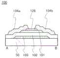
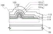
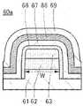
图5A至图5C是示出根据本发明的一个方式的晶体管的一个例子的图;5A to 5C are diagrams showing an example of a transistor according to an embodiment of the present invention;
图6A和图6B是示出根据本发明的一个方式的晶体管的一个例子的图;6A and 6B are diagrams showing an example of a transistor according to an embodiment of the present invention;
图7A和图7B是示出根据本发明的一个方式的晶体管的一个例子的图;7A and 7B are diagrams illustrating an example of a transistor according to an embodiment of the present invention;
图8A和图8B是示出根据本发明的一个方式的晶体管的一个例子的图;8A and 8B are diagrams showing an example of a transistor according to an embodiment of the present invention;
图9A至图9D是示出根据本发明的一个方式的晶体管的一个例子的图;9A to 9D are diagrams showing an example of a transistor according to an embodiment of the present invention;
图10A和图10B是示出根据本发明的一个方式的晶体管的一个例子的图;10A and 10B are diagrams showing an example of a transistor according to an embodiment of the present invention;
图11A至图11C是示出根据本发明的一个方式的晶体管的一个例子的图;11A to 11C are diagrams showing an example of a transistor according to an embodiment of the present invention;
图12A和图12B是根据本发明的一个方式的电路图;12A and 12B are circuit diagrams according to one embodiment of the present invention;
图13A至图13C是示出根据本发明的一个方式的半导体装置的一个例子的图;13A to 13C are diagrams showing an example of a semiconductor device according to an embodiment of the present invention;
图14A至图14C是示出根据本发明的一个方式的半导体装置的一个例子的图;14A to 14C are diagrams showing an example of a semiconductor device according to an embodiment of the present invention;
图15A至图15D是示出根据本发明的一个方式的半导体装置的一个例子的图;15A to 15D are diagrams showing an example of a semiconductor device according to an embodiment of the present invention;
图16A至图16E是示出根据本发明的一个方式的半导体装置的制造方法的图;16A to 16E are diagrams illustrating a method of manufacturing a semiconductor device according to one embodiment of the present invention;
图17A至图17D是示出根据本发明的一个方式的半导体装置的制造方法的图;17A to 17D are diagrams illustrating a method of manufacturing a semiconductor device according to one embodiment of the present invention;
图18A至图18C是示出根据本发明的一个方式的半导体装置的制造方法的图;18A to 18C are diagrams illustrating a method of manufacturing a semiconductor device according to one embodiment of the present invention;
图19A和图19B是示出根据本发明的一个方式的半导体装置的制造方法的图;19A and 19B are diagrams illustrating a method of manufacturing a semiconductor device according to one embodiment of the present invention;
图20A是示出根据本发明的一个方式的晶体管的一部分的能带结构的图,图20B是说明导通时的电流的路径的图;20A is a diagram illustrating an energy band structure of a part of a transistor according to one embodiment of the present invention, and FIG. 20B is a diagram illustrating a path of current during conduction;
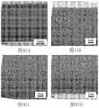
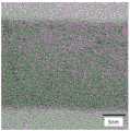
图21A至图21C是氧化物半导体的截面TEM图像及局部的傅立叶变换图像;21A to 21C are cross-sectional TEM images and local Fourier transform images of oxide semiconductors;
图22A至图22D是示出氧化物半导体膜的纳米束电子衍射图案的图及示出透射电子衍射测定装置的一个例子的图;22A to 22D are diagrams showing nanobeam electron diffraction patterns of oxide semiconductor films and diagrams showing an example of a transmission electron diffraction measurement device;
图23A至图23C是示出利用透射电子衍射测定的结构分析的一个例子的图及平面TEM图像;23A to 23C are diagrams and planar TEM images showing an example of structural analysis using transmission electron diffraction measurement;
图24A至图24D是根据实施方式的电路图;24A-24D are circuit diagrams according to embodiments;
图25是根据实施方式的RF标签的结构实例;25 is a structural example of an RF tag according to an embodiment;
图26是根据实施方式的CPU的结构实例;26 is a structural example of a CPU according to an embodiment;
图27是根据实施方式的存储元件的电路图;27 is a circuit diagram of a storage element according to an embodiment;
图28A至图28C是根据实施方式的显示装置的俯视图及电路图;28A to 28C are a top view and a circuit diagram of a display device according to an embodiment;
图29A至图29F是根据实施方式的电子设备;29A-29F are electronic devices according to embodiments;
图30A至图30F是根据实施方式的RF标签的使用例子;30A to 30F are usage examples of RF tags according to embodiments;
图31A至图31C是示出靶材的原子个数比和氧化物半导体膜的原子个数比的关系的图;31A to 31C are diagrams showing the relationship between the atomic number ratio of the target and the atomic number ratio of the oxide semiconductor film;
图32示出氧化物半导体膜的SIMS分析结果;FIG. 32 shows SIMS analysis results of oxide semiconductor films;
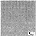
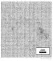
图33A和图33B示出氧化物半导体膜的截面TEM观察结果;33A and 33B show cross-sectional TEM observation results of the oxide semiconductor film;
图34A和图34B示出氧化物半导体膜的TDS分析结果;34A and 34B show the results of TDS analysis of the oxide semiconductor film;
图35A和图35B示出氧化物半导体膜的TDS分析结果;35A and 35B show TDS analysis results of the oxide semiconductor film;
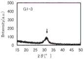
图36A至图36D示出根据本发明的一个方式的氧化物半导体膜的XRD评价结果;36A to 36D show XRD evaluation results of the oxide semiconductor film according to one embodiment of the present invention;
图37A和图37B示出氧化物半导体膜的截面TEM观察结果;37A and 37B show cross-sectional TEM observation results of the oxide semiconductor film;
图38A和图38B示出氧化物半导体膜的截面TEM观察结果;38A and 38B show cross-sectional TEM observation results of the oxide semiconductor film;
图39A和图39B示出氧化物半导体膜的截面TEM观察结果;39A and 39B show cross-sectional TEM observation results of the oxide semiconductor film;
图40A和图40B示出氧化物半导体膜的截面TEM观察结果;40A and 40B show cross-sectional TEM observation results of the oxide semiconductor film;
图41A至图41D示出氧化物半导体膜的截面TEM观察结果;41A to 41D show cross-sectional TEM observation results of the oxide semiconductor film;
图42A至图42D示出氧化物半导体膜的截面TEM观察结果;42A to 42D show cross-sectional TEM observation results of the oxide semiconductor film;
图43A和图43B示出氧化物半导体膜的平面TEM观察结果;43A and 43B show the results of planar TEM observation of the oxide semiconductor film;
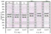
图44A和图44B是示出氧化物半导体膜的CAAC比率的图;44A and 44B are graphs showing CAAC ratios of oxide semiconductor films;
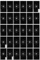
图45示出氧化物半导体膜的电子衍射图案;45 shows an electron diffraction pattern of an oxide semiconductor film;
图46示出氧化物半导体膜的电子衍射图案;46 shows an electron diffraction pattern of an oxide semiconductor film;
图47示出氧化物半导体膜的电子衍射图案;47 shows an electron diffraction pattern of an oxide semiconductor film;
图48示出氧化物半导体膜的电子衍射图案;48 shows an electron diffraction pattern of an oxide semiconductor film;
图49示出氧化物半导体膜的电子衍射图案;49 shows an electron diffraction pattern of an oxide semiconductor film;
图50示出氧化物半导体膜的电子衍射图案;FIG. 50 shows an electron diffraction pattern of an oxide semiconductor film;
图51示出氧化物半导体膜的电子衍射图案;51 shows an electron diffraction pattern of an oxide semiconductor film;
图52示出氧化物半导体膜的电子衍射图案;52 shows an electron diffraction pattern of an oxide semiconductor film;
图53示出氧化物半导体膜的电子衍射图案;53 shows an electron diffraction pattern of an oxide semiconductor film;
图54示出氧化物半导体膜的电子衍射图案;54 shows an electron diffraction pattern of an oxide semiconductor film;
图55示出氧化物半导体膜的平面TEM观察结果;FIG. 55 shows the results of planar TEM observation of the oxide semiconductor film;
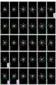
图56A至图56C示出氧化物半导体膜的电子衍射图案;56A to 56C illustrate electron diffraction patterns of oxide semiconductor films;
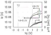
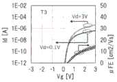
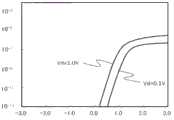
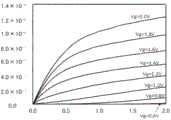
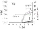
图57A和图57B是示出晶体管的Vg-Id特性的图;57A and 57B are graphs showing Vg-Id characteristics of transistors;
图58A和图58B是示出晶体管的Vg-Id特性的图;58A and 58B are graphs showing Vg-Id characteristics of transistors;
图59A和图59B示出氧化物半导体膜的截面TEM观察结果;59A and 59B show cross-sectional TEM observation results of the oxide semiconductor film;
图60是根据实施方式的半导体装置的电路图;60 is a circuit diagram of a semiconductor device according to an embodiment;
图61是说明In-Ga-Zn氧化物中的氧的移动路径的图;61 is a diagram illustrating the movement path of oxygen in In-Ga-Zn oxide;
图62A至图62C是示出根据本发明的一个方式的晶体管的一个例子的图;62A to 62C are diagrams showing an example of a transistor according to an embodiment of the present invention;
图63A和图63B是示出根据本发明的一个方式的晶体管的一个例子的图;63A and 63B are diagrams showing an example of a transistor according to an embodiment of the present invention;
图64A和图64B是示出根据本发明的一个方式的晶体管的一个例子的图;64A and 64B are diagrams showing an example of a transistor according to an embodiment of the present invention;
图65A至图65D是示出根据本发明的一个方式的晶体管的一个例子的图;65A to 65D are diagrams showing an example of a transistor according to an embodiment of the present invention;
图66A和图66B是示出根据本发明的一个方式的晶体管的一个例子的图;66A and 66B are diagrams showing an example of a transistor according to an embodiment of the present invention;
图67A和图67B是示出根据本发明的一个方式的晶体管的一个例子的图;67A and 67B are diagrams showing an example of a transistor according to an embodiment of the present invention;
图68A至图68C是示出根据本发明的一个方式的氧化物半导体膜的XRD评价结果;68A to 68C are diagrams showing XRD evaluation results of an oxide semiconductor film according to one embodiment of the present invention;
图69A至图69C是示出晶体管的Vg-Id特性的图;69A to 69C are graphs showing Vg-Id characteristics of transistors;
图70是示出晶体管的Vg-Id特性的图;FIG. 70 is a graph showing Vg-Id characteristics of a transistor;
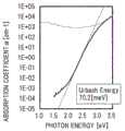
图71A和图71B示出氧化物半导体膜的CPM评价结果;71A and 71B show CPM evaluation results of oxide semiconductor films;
图72是示出晶体管的Vg-Id特性的图;FIG. 72 is a graph showing Vg-Id characteristics of a transistor;
图73是示出晶体管的阈值变化的图;FIG. 73 is a graph showing a change in threshold value of a transistor;
图74是示出晶体管的阈值变化的图;FIG. 74 is a graph showing a change in threshold value of a transistor;
图75是示出晶体管的阈值变化的图;FIG. 75 is a graph showing a change in threshold value of a transistor;
图76A和图76B是示出晶体管的Vg-Id特性的计算结果的图;76A and 76B are graphs showing calculation results of Vg-Id characteristics of transistors;
图77A和图77B是示出根据本发明的一个方式的晶体管的截面照片;77A and 77B are cross-sectional photographs showing a transistor according to one embodiment of the present invention;
图78是示出晶体管的Vg-Id特性的图;FIG. 78 is a graph showing Vg-Id characteristics of a transistor;
图79是示出晶体管的Vd-Id特性的图;FIG. 79 is a graph showing Vd-Id characteristics of a transistor;
图80A至图80C示出根据本发明的一个方式的氧化物的XRD评价结果;80A to 80C show XRD evaluation results of oxides according to one embodiment of the present invention;
图81A至图81D示出根据本发明的一个方式的氧化物的XRD评价结果;81A to 81D show XRD evaluation results of oxides according to one embodiment of the present invention;
图82A和图82B示出根据本发明的一个方式的氧化物的平面TEM观察结果;82A and 82B show planar TEM observations of oxides according to one embodiment of the present invention;
图83A和图83B示出根据本发明的一个方式的氧化物的平面TEM观察结果;83A and 83B illustrate planar TEM observations of oxides according to one embodiment of the present invention;
图84A和图84B示出根据本发明的一个方式的氧化物的平面TEM观察结果;84A and 84B illustrate planar TEM observations of oxides according to one embodiment of the present invention;
图85A和图85B是示出晶体管的Vg-Id特性的图;85A and 85B are graphs showing Vg-Id characteristics of transistors;
图86A和图86B是示出晶体管的Vg-Id特性的图;86A and 86B are graphs showing Vg-Id characteristics of transistors;
图87A和图87B是示出晶体管的Vg-Id特性的图;87A and 87B are graphs showing Vg-Id characteristics of transistors;
图88A和图88B是示出晶体管的Vg-Id特性的图;88A and 88B are graphs showing Vg-Id characteristics of transistors;
图89A和图89B是示出晶体管的Vg-Id特性的图。89A and 89B are graphs showing Vg-Id characteristics of transistors.
具体实施方式Detailed ways
参照附图对实施方式进行详细的说明。注意,本发明不局限于以下说明,而所属技术领域的普通技术人员可以很容易地理解一个事实就是其方式及详细内容在不脱离本发明的宗旨及其范围的情况下可以被变换为各种各样的形式。因此,本发明不应该被解释为仅局限于以下所示的实施方式所记载的内容中。Embodiments will be described in detail with reference to the accompanying drawings. Note that the present invention is not limited to the following description, and a person of ordinary skill in the art can easily understand the fact that the mode and details can be changed into various forms without departing from the spirit and scope of the present invention. various forms. Therefore, the present invention should not be construed as being limited to the contents described in the embodiments shown below.
注意,在下面说明的发明结构中,在不同的附图中共同使用相同的附图标记来表示相同的部分或具有相同功能的部分,而省略反复说明。此外,当表示具有相同功能的部分时有时使用相同的阴影线,而不特别附加附图标记。Note that, in the structure of the invention described below, the same reference numerals are commonly used in different drawings to denote the same parts or parts having the same functions, and repeated explanations are omitted. In addition, the same hatching is sometimes used when denoting parts having the same function, and a reference numeral is not particularly attached.
注意,在本说明书所说明的各个附图中,有时为了明确起见,夸大表示各构成要素的大小、层的厚度或区域。因此,本发明的一个方式并不限于附图中的比例。Note that in each of the drawings described in this specification, the size of each component, the thickness of a layer, or a region may be exaggerated for clarity. Therefore, one embodiment of the present invention is not limited to the scale in the drawings.
另外,在本说明书等中使用的“第一”、“第二”等序数词是为了方便识别构成要素而附的,而不是为了在数目方面上进行限定的。In addition, the ordinal numbers such as "first" and "second" used in the present specification and the like are attached for the convenience of identifying the constituent elements, and are not intended to limit the number.
注意,例如当导电性充分低时,有时即使表示为“半导体”也具有“绝缘体”的特性。此外,“半导体”和“绝缘体”的境界不太清楚,因此有时不能精确地区别。由此,有时可以将本说明书所记载的“半导体”换称为“绝缘体”。同样地,有时可以将本说明书所记载的“绝缘体”换称为“半导体”。Note that, for example, when the electrical conductivity is sufficiently low, even if it is expressed as a "semiconductor", it may have the characteristics of an "insulator". Furthermore, the boundaries of "semiconductor" and "insulator" are not very clear, so sometimes the distinction cannot be made precisely. Therefore, the "semiconductor" described in this specification may be referred to as an "insulator" in some cases. Similarly, the "insulator" described in this specification may be referred to as a "semiconductor" in some cases.
晶体管是半导体元件的一种,可以进行电流或电压的放大、控制导通或非导通的开关动作等。本说明书中的晶体管包括IGFET(Insulated Gate Field EffectTransistor:绝缘栅场效应晶体管)和薄膜晶体管(TFT:Thin Film Transistor)。A transistor is a type of semiconductor element, and can amplify current or voltage, control conduction or non-conduction switching, and the like. The transistor in this specification includes IGFET (Insulated Gate Field Effect Transistor: Insulated Gate Field Effect Transistor) and Thin Film Transistor (TFT: Thin Film Transistor).
另外,根据情况或状态,可以互相调换“膜”和“层”。例如,有时可以将“导电层”调换为“导电膜”。另外,有时可以将“绝缘膜”调换为“绝缘层”。In addition, "film" and "layer" may be interchanged with each other depending on the situation or state. For example, "conductive layer" may be interchanged with "conductive film" in some cases. In addition, "insulating film" may be interchanged with "insulating layer" in some cases.
实施方式1
在本实施方式中,说明本发明的一个方式的氧化物半导体。In this embodiment mode, an oxide semiconductor according to one embodiment of the present invention will be described.
在此,氧化物半导体例如是包含铟的氧化物半导体。在氧化物半导体包含铟时,例如其载流子迁移率(电子迁移率)提高。另外,氧化物半导体优选包含元素M。元素M优选是铝、镓、钇或锡等。作为可用作元素M的其他元素,有硼、硅、钛、铁、镍、锗、钇、锆、钼、镧、铈、钕、铪、钽、钨等。注意,作为元素M有时也可以组合多个上述元素。元素M例如是与氧的键能高的元素。元素M例如是与氧的键能高于铟的元素。或者,元素M例如是具有增大氧化物半导体的能隙的功能的元素。此外,氧化物半导体优选包含锌。当氧化物半导体包含锌时,有时容易晶化。Here, the oxide semiconductor is, for example, an oxide semiconductor containing indium. When the oxide semiconductor contains indium, for example, the carrier mobility (electron mobility) thereof increases. In addition, the oxide semiconductor preferably contains element M. The element M is preferably aluminum, gallium, yttrium or tin or the like. As other elements that can be used as the element M, there are boron, silicon, titanium, iron, nickel, germanium, yttrium, zirconium, molybdenum, lanthanum, cerium, neodymium, hafnium, tantalum, tungsten, and the like. Note that, as the element M, a plurality of the above-mentioned elements may be combined in some cases. The element M is, for example, an element having a high bond energy with oxygen. The element M is, for example, an element whose bond energy with oxygen is higher than that of indium. Alternatively, the element M is, for example, an element having a function of increasing the energy gap of the oxide semiconductor. Further, the oxide semiconductor preferably contains zinc. When the oxide semiconductor contains zinc, crystallization is sometimes easy.
[氧化物半导体膜的结构][Structure of Oxide Semiconductor Film]
以下说明氧化物半导体膜的结构。The structure of the oxide semiconductor film will be described below.
氧化物半导体膜大致分为非单晶氧化物半导体膜和单晶氧化物半导体膜。非单晶氧化物半导体膜包括CAAC-OS(C-Axis Aligned Crystalline Oxide Semiconductor:c轴取向结晶氧化物半导体)膜、多晶氧化物半导体膜、微晶氧化物半导体膜以及非晶氧化物半导体膜等。Oxide semiconductor films are roughly classified into non-single crystal oxide semiconductor films and single crystal oxide semiconductor films. Non-single crystal oxide semiconductor films include CAAC-OS (C-Axis Aligned Crystalline Oxide Semiconductor) films, polycrystalline oxide semiconductor films, microcrystalline oxide semiconductor films, and amorphous oxide semiconductor films Wait.
首先,说明CAAC-OS膜。First, the CAAC-OS film will be described.
CAAC-OS膜是包含呈c轴取向的多个结晶部的氧化物半导体膜之一。The CAAC-OS film is one of oxide semiconductor films including a plurality of crystal parts in a c-axis orientation.
通过利用透射电子显微镜(TEM:Transmission Electron Microscope)观察CAAC-OS膜的亮视场像及衍射图案的复合分析图像(也称为高分辨率TEM图像),可以确认到多个结晶部。另一方面,通过高分辨率TEM也观察不到结晶部与结晶部之间的明确的边界,即晶界(grain boundary)。因此,在CAAC-OS膜中,不容易发生由晶界引起的电子迁移率的下降。By observing the bright field image of the CAAC-OS film and the composite analysis image of the diffraction pattern (also referred to as a high-resolution TEM image) with a transmission electron microscope (TEM: Transmission Electron Microscope), a plurality of crystal parts were confirmed. On the other hand, clear boundaries between crystal parts, ie, grain boundaries, were not observed by high-resolution TEM. Therefore, in the CAAC-OS film, a decrease in electron mobility due to grain boundaries does not easily occur.
根据从大致平行于样品面的方向观察的CAAC-OS膜的高分辨率截面TEM图像可知在结晶部中金属原子排列为层状。各金属原子层具有反映形成CAAC-OS膜的面(也称为被形成面)或CAAC-OS膜的顶面的凸凹的形状并以平行于CAAC-OS膜的被形成面或顶面的方式排列。From the high-resolution cross-sectional TEM image of the CAAC-OS film observed from a direction substantially parallel to the sample surface, it can be seen that metal atoms are arranged in layers in the crystal portion. Each metal atomic layer has a shape reflecting the convex and concave shape of the surface on which the CAAC-OS film is formed (also referred to as the surface to be formed) or the top surface of the CAAC-OS film and is parallel to the surface to be formed or the top surface of the CAAC-OS film. arrangement.
另一方面,当从大致垂直于样品面的方向观察CAAC-OS膜的高分辨率平面TEM图像时,可以确认到在结晶部中金属原子排列为三角形状或六边形状。但是,在不同的结晶部之间金属原子的排列没有规律性。On the other hand, when a high-resolution planar TEM image of the CAAC-OS film was observed from a direction substantially perpendicular to the sample surface, it was confirmed that the metal atoms were arranged in a triangular or hexagonal shape in the crystal portion. However, there is no regularity in the arrangement of metal atoms between different crystal parts.
在本说明书中,“平行”是指两条直线形成的角度为-10°以上且10°以下的状态。因此,也包括该角度为-5°以上且5°以下的状态。“大致平行”是指两条直线形成的角度为-30°以上且30°以下的状态。另外,“垂直”是指两条直线形成的角度为80°以上且100°以下的状态。因此也包括85°以上且95°以下的角度的状态。“大致垂直”是指两条直线形成的角度为60°以上且120°以下的状态。In this specification, "parallel" refers to a state where the angle formed by two straight lines is -10° or more and 10° or less. Therefore, the state where this angle is -5° or more and 5° or less is also included. "Substantially parallel" refers to a state where the angle formed by the two straight lines is -30° or more and 30° or less. In addition, "perpendicular" refers to a state in which the angle formed by two straight lines is 80° or more and 100° or less. Therefore, the state of the angle of 85° or more and 95° or less is also included. "Substantially perpendicular" refers to a state where the angle formed by two straight lines is 60° or more and 120° or less.
在本说明书中,六方晶系包括三方晶系和菱方晶系。In this specification, the hexagonal crystal system includes the trigonal crystal system and the rhombohedral crystal system.
图21A是CAAC-OS膜的截面的高分辨率TEM图像。另外,图21B是进一步放大图21A的截面的高分辨率TEM图像,其中,为便于理解而突出显示原子排列。Figure 21A is a high-resolution TEM image of a cross-section of the CAAC-OS film. In addition, FIG. 21B is a high-resolution TEM image further magnifying the cross-section of FIG. 21A, in which the atomic arrangement is highlighted for ease of understanding.
图21C是图21A中的A-O-A’之间的由圆圈包围的区域(直径大致为4nm)的局部性的傅立叶变换图像。在图21C所示的各区域中可以确认到c轴取向性。另外,A-O间的c轴方向不同于O-A’间的c轴方向,由此可知A-O间的晶粒不同于O-A’间的晶粒。另外,可知在A-O之间,c轴的角度以14.3°、16.6°、26.4°等而逐渐地连续变化。同样地,可知在O-A’之间,c轴的角度以-18.3°、-17.6°、-15.9°等而逐渐地连续变化。Fig. 21C is a localized Fourier transform image of the area (approximately 4 nm in diameter) surrounded by a circle between A-O-A' in Fig. 21A . The c-axis orientation was confirmed in each region shown in FIG. 21C . In addition, the c-axis direction between A-O is different from the c-axis direction between O-A', so that the crystal grains between A-O are different from those between O-A'. In addition, it can be seen that between A-O, the angle of the c-axis is gradually and continuously changed at 14.3°, 16.6°, 26.4°, and the like. Similarly, it can be seen that between O-A', the angle of the c-axis gradually changes continuously at -18.3°, -17.6°, -15.9°, and the like.
另外,在CAAC-OS膜的电子衍射图案中,观察到呈现取向性的斑点(亮点)。例如,在使用例如为1nm以上且30nm以下的电子束获得的CAAC-OS膜的顶面的电子衍射图案(也称为纳米束电子衍射图案)中,观察到斑点(参照图22A)。In addition, in the electron diffraction pattern of the CAAC-OS film, oriented spots (bright spots) were observed. For example, in the electron diffraction pattern (also referred to as nanobeam electron diffraction pattern) of the top surface of the CAAC-OS film obtained using, for example, an electron beam of 1 nm or more and 30 nm or less, spots are observed (see FIG. 22A ).
由截面的高分辨率TEM图像及平面的高分辨率TEM图像可知,CAAC-OS膜的结晶部具有取向性。From the high-resolution TEM image of the cross section and the high-resolution TEM image of the plane, it was found that the crystal part of the CAAC-OS film had orientation.
注意,CAAC-OS膜所包含的结晶部几乎都可以容纳在一个边长小于100nm的立方体内。因此,有时包括在CAAC-OS膜中的结晶部能够容纳在一边短于10nm、短于5nm或短于3nm的立方体。但是,有时包含在CAAC-OS膜中的多个结晶部联结,从而形成一个大结晶区域。例如,在平面的高分辨率TEM图像中有时会观察到2500nm2以上、5μm2以上或1000μm2以上的结晶区域。Note that almost all the crystal parts contained in the CAAC-OS film can be accommodated in a cube with side lengths less than 100 nm. Therefore, the crystal part sometimes included in the CAAC-OS film can be accommodated in a cube whose one side is shorter than 10 nm, shorter than 5 nm, or shorter than 3 nm. However, a plurality of crystal parts included in the CAAC-OS film are sometimes connected to form one large crystal region. For example, a crystalline region of 2500 nm2 or more, 5 μm2 or more, or 1000 μm2 or more may be observed in a planar high-resolution TEM image.
使用X射线衍射(XRD:X-Ray Diffraction)装置对CAAC-OS膜进行结构分析。例如,当利用out-of-plane法分析包括InGaZnO4结晶的CAAC-OS膜时,在衍射角(2θ)为31°附近时常出现峰值。由于该峰值来源于InGaZnO4结晶的(009)面,由此可知CAAC-OS膜中的结晶具有c轴取向性,并且c轴朝向大致垂直于CAAC-OS膜的被形成面或顶面的方向。Structural analysis of the CAAC-OS films was performed using an X-ray diffraction (XRD: X-Ray Diffraction) device. For example, when a CAAC-OS film including InGaZnO4 crystals is analyzed by the out-of-plane method, a peak often appears around a diffraction angle (2θ) of 31°. Since this peak originates from the (009) plane of the InGaZnO4 crystal, it can be seen that the crystal in the CAAC-OS film has c-axis orientation, and the c-axis is oriented in a direction substantially perpendicular to the surface on which the CAAC-OS film is formed or the top surface .
另一方面,当利用从大致垂直于c轴的方向使X射线入射到样品的in-plane法分析CAAC-OS膜时,在2θ为56°附近时常出现峰值。该峰值来源于InGaZnO4结晶的(110)面。在此,将2θ固定为56°附近并在以样品面的法线向量为轴(


由上述结果可知,在具有c轴取向的CAAC-OS膜中,虽然a轴及b轴的方向在不同结晶部之间不规律,但是c轴都朝向平行于被形成面或顶面的法线向量的方向。因此,在上述截面的高分辨率TEM图像中观察到的排列为层状的各金属原子层相当于与结晶的ab面平行的面。From the above results, it can be seen that in the CAAC-OS film with c-axis orientation, although the directions of the a-axis and b-axis are irregular between different crystal parts, the c-axis is oriented parallel to the normal line of the surface to be formed or the top surface. direction of the vector. Therefore, each metal atomic layer arranged in a layered shape observed in the high-resolution TEM image of the cross section corresponds to a plane parallel to the ab plane of the crystal.
注意,结晶部在形成CAAC-OS膜或进行加热处理等晶化处理时形成。如上所述,结晶的c轴朝向平行于CAAC-OS膜的被形成面或顶面的法线向量的方向。由此,例如,当CAAC-OS膜的形状因蚀刻等而发生改变时,结晶的c轴不一定平行于CAAC-OS膜的被形成面或顶面的法线向量。Note that the crystallized portion is formed when forming the CAAC-OS film or performing crystallization treatment such as heat treatment. As described above, the c-axis of the crystal is oriented in the direction parallel to the normal vector of the surface or top surface of the CAAC-OS film. Thus, for example, when the shape of the CAAC-OS film is changed by etching or the like, the c-axis of the crystal is not necessarily parallel to the normal vector of the surface on which the CAAC-OS film is formed or the top surface.
另外,在CAAC-OS膜中,c轴取向的晶化部的分布不一定要均匀。例如,当CAAC-OS膜的结晶部是由CAAC-OS膜的顶面附近的结晶成长而形成时,有时顶面附近的c轴取向的结晶部比例会高于被形成面附近的晶化度。另外,在添加有杂质的CAAC-OS膜中,添加有杂质的区域变质而有时CAAC-OS膜中的c轴取向结晶部所占的比例根据区域而不同。In addition, in the CAAC-OS film, the distribution of the c-axis-oriented crystallized portion does not necessarily have to be uniform. For example, when the crystal part of the CAAC-OS film is formed by the growth of the crystal near the top surface of the CAAC-OS film, the proportion of the c-axis-oriented crystal part near the top surface may be higher than the crystallinity degree near the surface to be formed. . In addition, in the impurity-added CAAC-OS film, the region to which the impurity is added is degraded, and the proportion of the c-axis-oriented crystal part in the CAAC-OS film may vary depending on the region.
注意,当利用out-of-plane法分析包括InGaZnO4结晶的CAAC-OS膜时,除了在2θ为31°附近的峰值之外,有时还在2θ为36°附近观察到峰值。2θ为36°附近的峰值意味着CAAC-OS膜的一部分中含有不具有c轴取向的结晶,例如典型为尖晶石型结晶结构。优选的是,在CAAC-OS膜中在2θ为31°附近时出现峰值而在2θ为36°附近时不出现峰值。Note that when the CAAC-OS film including the InGaZnO4 crystal was analyzed by the out-of-plane method, in addition to the peak around 31° in 2θ, a peak was sometimes observed around 36° in 2θ. A peak near 36° in 2θ means that a part of the CAAC-OS film contains crystals that do not have c-axis orientation, for example, typically a spinel-type crystal structure. Preferably, in the CAAC-OS film, the peak appears when 2θ is around 31° and the peak does not appear when 2θ is around 36°.
CAAC-OS膜是杂质浓度低的氧化物半导体膜。杂质是指氢、碳、硅、过渡金属元素等氧化物半导体膜的主要成分以外的元素。尤其是,某一种元素如硅等与氧的键合力比构成氧化物半导体膜的金属元素与氧的键合力强,该元素会夺取氧化物半导体膜中的氧,从而打乱氧化物半导体膜的原子排列,导致结晶性下降。另外,由于铁或镍等的重金属、氩、二氧化碳等的原子半径(或分子半径)大,所以若包含在氧化物半导体膜内,则会打乱氧化物半导体膜的原子排列,导致结晶性下降。注意,包含在氧化物半导体膜中的杂质有时成为载流子陷阱或载流子发生源。The CAAC-OS film is an oxide semiconductor film with a low impurity concentration. Impurities refer to elements other than the main components of the oxide semiconductor film such as hydrogen, carbon, silicon, and transition metal elements. In particular, a certain element such as silicon has a stronger bonding force with oxygen than a metal element constituting the oxide semiconductor film and oxygen, and the element robs oxygen in the oxide semiconductor film, thereby disturbing the oxide semiconductor film. atomic arrangement, resulting in a decrease in crystallinity. In addition, heavy metals such as iron and nickel, argon, carbon dioxide, and the like have large atomic radii (or molecular radii), so if they are contained in the oxide semiconductor film, the atomic arrangement of the oxide semiconductor film is disturbed, resulting in a decrease in crystallinity . Note that impurities contained in the oxide semiconductor film may become a carrier trap or a carrier generation source.
另外,CAAC-OS膜是缺陷态密度低的氧化物半导体膜。例如,氧化物半导体膜中的氧缺陷有时成为载流子陷阱,或因俘获氢而成为载流子发生源。In addition, the CAAC-OS film is an oxide semiconductor film with a low density of defect states. For example, oxygen vacancies in the oxide semiconductor film may become carrier traps or become a carrier generation source by trapping hydrogen.
将杂质浓度低且缺陷态密度低(氧缺陷量少)的状态称为“高纯度本征”或“实质上高纯度本征”。在高纯度本征或实质上高纯度本征的氧化物半导体膜中载流子发生源少,所以可以降低载流子密度。在此,说明将该氧化物半导体膜用于晶体管的情况。使用该氧化物半导体膜的晶体管很少具有负阈值电压的电特性(也称为常开启特性)。在高纯度本征或实质上高纯度本征的氧化物半导体膜中载流子陷阱少。因此,使用该氧化物半导体膜的晶体管的电特性变动小,于是成为高可靠性晶体管。另外,被氧化物半导体膜的载流子陷阱俘获的电荷的释放需要长时间,有时像固定电荷那样动作。因此,使用杂质浓度高且缺陷态密度高的氧化物半导体膜的晶体管的电特性有时不稳定。杂质及氧缺陷少的CAAC-OS膜是载流子密度低的氧化物半导体。具体而言,可以使用载流子密度小于8×10¹¹/cm3、优选小于1×1011/cm3、更优选小于1×1010/cm3、且是1×10-9/cm3以上的氧化物半导体。将这样的氧化物半导体称为高纯度本征或实质上高纯度本征的氧化物半导体。CAAC-OS膜的杂质浓度和缺陷态密度低。即,CAAC-OS膜可以说是具有稳定的特性的氧化物半导体。A state with a low impurity concentration and a low density of defect states (a small amount of oxygen vacancies) is referred to as "high-purity intrinsic" or "substantially high-purity intrinsic". In a high-purity intrinsic or substantially high-purity intrinsic oxide semiconductor film, there are few sources of carrier generation, so the carrier density can be reduced. Here, the case where this oxide semiconductor film is used for a transistor will be described. Transistors using this oxide semiconductor film rarely have electrical characteristics of a negative threshold voltage (also referred to as normally-on characteristics). There are few carrier traps in a high-purity intrinsic or substantially high-purity intrinsic oxide semiconductor film. Therefore, a transistor using this oxide semiconductor film has little variation in electrical characteristics, and thus becomes a highly reliable transistor. In addition, it takes a long time to release the charges trapped in the carrier traps of the oxide semiconductor film, and it may act like a fixed charge. Therefore, the electrical characteristics of a transistor using an oxide semiconductor film having a high impurity concentration and a high density of defect states may be unstable in some cases. The CAAC-OS film with few impurities and oxygen vacancies is an oxide semiconductor with low carrier density. Specifically, a carrier density of less than 8 × 10¹¹ /cm3 , preferably less than 1 × 10¹¹ /cm3 , more preferably less than 1 × 10¹⁰ /cm3 , and 1 × 10⁻⁹ /cm3 can be used the above oxide semiconductors. Such an oxide semiconductor is called a high-purity intrinsic or substantially high-purity intrinsic oxide semiconductor. The impurity concentration and defect state density of the CAAC-OS film are low. That is, the CAAC-OS film can be said to be an oxide semiconductor having stable characteristics.
另外,在使用CAAC-OS膜的晶体管中,起因于可见光或紫外光的照射的电特性的变动小。In addition, in the transistor using the CAAC-OS film, fluctuations in electrical properties due to irradiation with visible light or ultraviolet light are small.
接下来,对多晶氧化物半导体膜进行说明。Next, the polycrystalline oxide semiconductor film will be described.
在多晶氧化物半导体膜的高分辨率TEM图像中,可以观察到晶粒。例如在高分辨率TEM图像中,多晶氧化物半导体膜中含有的晶粒的粒径尺寸大多为2nm以上且300nm以下、3nm以上且100nm以下或5nm以上且50nm以下。另外,在多晶氧化物半导体膜的高分辨率TEM图像中,有时观察到晶界。In the high-resolution TEM image of the polycrystalline oxide semiconductor film, crystal grains can be observed. For example, in a high-resolution TEM image, the grain size of crystal grains contained in the polycrystalline oxide semiconductor film is often 2 nm or more and 300 nm or less, 3 nm or more and 100 nm or less, or 5 nm or more and 50 nm or less. In addition, in the high-resolution TEM image of the polycrystalline oxide semiconductor film, grain boundaries are sometimes observed.
多晶氧化物半导体膜包含多个晶粒,并且,在该多个晶粒之间结晶取向有时不同。另外,使用XRD装置对多晶氧化物半导体膜进行结构分析。例如,当利用out-of-plane法分析包括InGaZnO4结晶的多晶氧化物半导体膜时,有时在2θ为31°或36°等附近时出现峰值。The polycrystalline oxide semiconductor film includes a plurality of crystal grains, and the crystal orientation may be different among the plurality of crystal grains. In addition, the polycrystalline oxide semiconductor film was subjected to structural analysis using an XRD apparatus. For example, when a polycrystalline oxide semiconductor film including InGaZnO4 crystals is analyzed by the out-of-plane method, a peak may appear when 2θ is around 31° or 36° or the like.
由于多晶氧化物半导体膜具有高结晶性,因此有时具有高电子迁移率。所以,使用多晶氧化物半导体膜的晶体管具有高场效应迁移率。注意,有时在多晶氧化物半导体膜中,杂质偏析在晶界。另外,多晶氧化物半导体膜的晶界成为缺陷能级。多晶氧化物半导体膜的晶界有可能成为载流子陷阱或载流子发生源,因此有时与使用CAAC-OS膜的晶体管相比,使用多晶氧化物半导体膜的晶体管的电特性变动大,而成为可靠性低的晶体管。Since the polycrystalline oxide semiconductor film has high crystallinity, it sometimes has high electron mobility. Therefore, the transistor using the polycrystalline oxide semiconductor film has high field effect mobility. Note that, in a polycrystalline oxide semiconductor film, impurities are sometimes segregated at grain boundaries. In addition, the grain boundary of the polycrystalline oxide semiconductor film becomes a defect level. The grain boundary of the polycrystalline oxide semiconductor film may become a carrier trap or a carrier generation source. Therefore, the electrical characteristics of the transistor using the polycrystalline oxide semiconductor film may vary greatly compared with the transistor using the CAAC-OS film. , and become a transistor with low reliability.
接下来,说明微晶氧化物半导体膜。Next, the microcrystalline oxide semiconductor film will be described.
在高分辨率TEM图像中,微晶氧化物半导体膜包括能够确认到结晶部的区域以及不能够明确地确认到结晶部的区域。微晶氧化物半导体膜中含有的结晶部的尺寸大多为1nm以上且100nm以下或1nm以上且10nm以下。尤其是,将具有尺寸为1nm以上且10nm以下或1nm以上且3nm以下的微晶的纳米晶(nc:nanocrystal)的氧化物半导体膜称为nc-OS(nanocrystalline Oxide Semiconductor:纳米晶氧化物半导体)膜。另外,例如在nc-OS膜的高分辨率TEM图像中,有时难以明确地确认到晶界。In the high-resolution TEM image, the microcrystalline oxide semiconductor film includes a region where a crystal part can be recognized and a region where the crystal part cannot be clearly recognized. The size of the crystal part contained in the microcrystalline oxide semiconductor film is often 1 nm or more and 100 nm or less, or 1 nm or more and 10 nm or less. In particular, an oxide semiconductor film of nanocrystals (nc: nanocrystals) having crystallites having a size of 1 nm or more and 10 nm or less or 1 nm or more and 3 nm or less is called nc-OS (nanocrystalline Oxide Semiconductor: nanocrystalline oxide semiconductor). membrane. In addition, for example, in a high-resolution TEM image of an nc-OS film, it may be difficult to clearly identify grain boundaries.
nc-OS膜在微小区域(例如1nm以上且10nm以下的区域,特别是1nm以上且3nm以下的区域)中其原子排列具有周期性。另外,nc-OS膜在不同的结晶部之间观察不到晶体取向的规律性。因此,在膜整体上观察不到取向性。所以,有时nc-OS膜在某些分析方法中与非晶氧化物半导体膜没有差别。例如,在通过利用使用其束径比结晶部大的X射线的XRD装置的out-of-plane法对nc-OS膜进行结构分析时,检测不出表示结晶面的峰值。另外,在对nc-OS膜进行使用其束径比结晶部大(例如,50nm以上)的电子射线的电子衍射(也称为选区电子衍射)时,观察到类似于光晕图案的衍射图案。另一方面,在对nc-OS膜进行使用其束径近于或小于结晶部的电子射线的纳米束电子衍射时,观察到斑点。另外,在nc-OS膜的纳米束电子衍射图案中,有时观察到如圆圈那样的(环状的)亮度高的区域。在nc-OS膜的纳米束电子衍射图案中,还有时观察到环状的区域内的多个斑点(参照图22B)。The atomic arrangement of the nc-OS film has periodicity in a minute region (for example, a region of 1 nm or more and 10 nm or less, in particular, a region of 1 nm or more and 3 nm or less). In addition, in the nc-OS film, the regularity of crystal orientation was not observed between different crystal parts. Therefore, no orientation was observed in the entire film. Therefore, sometimes the nc-OS film does not differ from the amorphous oxide semiconductor film in some analysis methods. For example, when the structure of the nc-OS film is analyzed by the out-of-plane method using an X-ray XRD apparatus having a beam diameter larger than that of the crystal portion, no peak indicating the crystal plane is detected. In addition, when electron diffraction (also referred to as selected area electron diffraction) using electron rays having a beam diameter larger than that of the crystal part (eg, 50 nm or more) was performed on the nc-OS film, a diffraction pattern similar to a halo pattern was observed. On the other hand, when the nc-OS film was subjected to nanobeam electron diffraction using electron rays whose beam diameter was close to or smaller than that of the crystal portion, spots were observed. In addition, in the nanobeam electron diffraction pattern of the nc-OS film, a region with high brightness such as a circle (annular) may be observed. In the nanobeam electron diffraction pattern of the nc-OS film, a plurality of spots in a ring-shaped region were sometimes observed (see FIG. 22B ).
nc-OS膜是其规律性比非晶氧化物半导体膜高的氧化物半导体膜。因此,nc-OS膜的缺陷态密度比非晶氧化物半导体膜低。但是,nc-OS膜在不同的结晶部之间观察不到晶体取向的规律性。所以,nc-OS膜的缺陷态密度比CAAC-OS膜高。The nc-OS film is an oxide semiconductor film whose regularity is higher than that of the amorphous oxide semiconductor film. Therefore, the density of defect states of the nc-OS film is lower than that of the amorphous oxide semiconductor film. However, in the nc-OS film, the regularity of crystal orientation was not observed between different crystal parts. Therefore, the defect state density of nc-OS films is higher than that of CAAC-OS films.
因此,nc-OS膜有时具有比CAAC-OS膜高的载流子密度。载流子密度高的氧化物半导体膜有时具有高电子迁移率。所以,使用nc-OS膜的晶体管有时具有较高的场效应迁移率。此外,因为nc-OS膜有时具有比CAAC-OS膜高的缺陷态密度,所以有时具有较多的载流子陷阱。因此,与使用CAAC-OS膜的晶体管相比,使用nc-OS膜的晶体管的电特性变动大,而成为可靠性低的晶体管。注意,因为nc-OS膜即使包含较多的杂质也可以形成,所以与CAAC-OS膜相比容易形成,从而有时根据用途优选使用nc-OS膜。因此,有时能够高生产率地制造具有使用nc-OS膜的晶体管的半导体装置。Therefore, the nc-OS film sometimes has a higher carrier density than the CAAC-OS film. Oxide semiconductor films with high carrier density sometimes have high electron mobility. Therefore, transistors using nc-OS films sometimes have high field-effect mobility. In addition, since the nc-OS film sometimes has a higher density of defect states than the CAAC-OS film, it sometimes has more carrier traps. Therefore, compared with the transistor using the CAAC-OS film, the electrical characteristics of the transistor using the nc-OS film fluctuate greatly, and the transistor has low reliability. Note that since the nc-OS film can be formed even if it contains a large amount of impurities, it is easier to form than the CAAC-OS film, so that the nc-OS film may be preferably used depending on the application. Therefore, a semiconductor device having a transistor using an nc-OS film can sometimes be manufactured with high productivity.
接着,对非晶氧化物半导体膜进行说明。Next, the amorphous oxide semiconductor film will be described.
非晶氧化物半导体膜是具有无序的原子排列并不具有结晶部的氧化物半导体膜。其一个例子为具有如石英那样的无定形状态的氧化物半导体膜。The amorphous oxide semiconductor film is an oxide semiconductor film having a disordered atomic arrangement and no crystal part. An example of this is an oxide semiconductor film having an amorphous state such as quartz.
在使用高分辨率TEM观察的非晶氧化物半导体膜的图像中,观察不到结晶部。In the image of the amorphous oxide semiconductor film observed using a high-resolution TEM, no crystal portion was observed.
使用XRD装置对非晶氧化物半导体膜进行结构分析。当利用out-of-plane法分析时,检测不到表示结晶面的峰值。另外,在对非晶氧化物半导体膜进行电子衍射时,观察到光晕图案。另外,在对非晶氧化物半导体膜进行纳米束电子衍射时,观察不到斑点,而观察到光晕图案。The amorphous oxide semiconductor film was subjected to structural analysis using an XRD apparatus. When analyzed by the out-of-plane method, no peak indicating a crystal plane was detected. In addition, when the amorphous oxide semiconductor film was subjected to electron diffraction, a halo pattern was observed. In addition, when the amorphous oxide semiconductor film was subjected to nanobeam electron diffraction, no spots were observed, but a halo pattern was observed.
非晶氧化物半导体膜是以高的浓度包含氢等杂质的氧化物半导体膜。此外,非晶氧化物半导体膜是其缺陷态密度高的氧化物半导体膜。The amorphous oxide semiconductor film is an oxide semiconductor film containing impurities such as hydrogen at a high concentration. In addition, the amorphous oxide semiconductor film is an oxide semiconductor film having a high density of defect states.
杂质浓度高且缺陷态密度高的氧化物半导体膜是载流子陷阱或载流子发生源多的氧化物半导体膜。An oxide semiconductor film with a high impurity concentration and a high density of defect states is an oxide semiconductor film with many carrier traps or carrier generation sources.
因此,非晶氧化物半导体膜有时具有比nc-OS膜更高的载流子密度。所以,使用非晶氧化物半导体膜的晶体管容易具有常导通电特性。因此,有时可以将非晶氧化物半导体膜适用于需要常导通电特性的晶体管。非晶氧化物半导体膜具有较高的缺陷态密度,因此有时具有较多的载流子陷阱。由此,与使用CAAC-OS膜或nc-OS膜的晶体管相比,使用非晶氧化物半导体膜的晶体管的电特性变动大,而成为可靠性低的晶体管。Therefore, the amorphous oxide semiconductor film sometimes has a higher carrier density than the nc-OS film. Therefore, a transistor using an amorphous oxide semiconductor film tends to have normally-on characteristics. Therefore, an amorphous oxide semiconductor film may be applied to a transistor that requires always-on characteristics. The amorphous oxide semiconductor film has a high density of defect states, and therefore sometimes has many carrier traps. As a result, compared with the transistor using the CAAC-OS film or the nc-OS film, the electrical characteristics of the transistor using the amorphous oxide semiconductor film fluctuate greatly, resulting in a low-reliability transistor.
接着,对单晶氧化物半导体膜进行说明。Next, the single crystal oxide semiconductor film will be described.
单晶氧化物半导体膜是杂质浓度低且缺陷态密度低(氧缺陷少)的氧化物半导体膜。所以,可以降低载流子密度。因此,使用单晶氧化物半导体膜的晶体管很少具有常导通电特性。另外,由于单晶氧化物半导体膜具有较低的杂质浓度和较低的缺陷态密度,因此有时具有很少的载流子陷阱。因此,使用单晶氧化物半导体膜的晶体管的电特性变动小,而成为可靠性高的晶体管。The single crystal oxide semiconductor film is an oxide semiconductor film having a low impurity concentration and a low density of defect states (less oxygen defects). Therefore, the carrier density can be reduced. Therefore, transistors using a single crystal oxide semiconductor film rarely have normally-on characteristics. In addition, since the single crystal oxide semiconductor film has a low impurity concentration and a low density of defect states, it sometimes has few carrier traps. Therefore, a transistor using a single crystal oxide semiconductor film has little variation in electrical characteristics, and thus becomes a transistor with high reliability.
为了形成单晶,例如能够以大约1000℃以上的高温度进行焙烧。另一方面,CAAC-OS膜能够以室温至500℃左右的低温度形成,所以在产业上是优选的。In order to form a single crystal, it can be fired at a high temperature of about 1000°C or higher, for example. On the other hand, since the CAAC-OS film can be formed at a low temperature ranging from room temperature to about 500° C., it is industrially preferable.
注意,氧化物半导体膜的缺陷越少其密度越高。此外,氧化物半导体膜的结晶性越高其密度越高。另外,当氧化物半导体膜中的氢等杂质的浓度越低其密度越高。单晶氧化物半导体膜的密度比CAAC-OS膜高。此外,CAAC-OS膜的密度比微晶氧化物半导体膜高。另外,多晶氧化物半导体膜的密度比微晶氧化物半导体膜高。此外,微晶氧化物半导体膜的密度比非晶氧化物半导体膜高。Note that the density of the oxide semiconductor film is higher with fewer defects. In addition, the higher the crystallinity of the oxide semiconductor film, the higher the density. In addition, as the concentration of impurities such as hydrogen in the oxide semiconductor film is lower, the density is higher. The density of the single crystal oxide semiconductor film is higher than that of the CAAC-OS film. In addition, the density of the CAAC-OS film is higher than that of the microcrystalline oxide semiconductor film. In addition, the density of the polycrystalline oxide semiconductor film is higher than that of the microcrystalline oxide semiconductor film. In addition, the density of the microcrystalline oxide semiconductor film is higher than that of the amorphous oxide semiconductor film.
此外,氧化物半导体膜有时具有呈现nc-OS膜与非晶氧化物半导体膜之间的物性的结构。将具有这种结构的氧化物半导体膜特别称为amorphous-like氧化物半导体(a-like OS:amorphous-like Oxide Semiconductor)膜。In addition, the oxide semiconductor film may have a structure that exhibits physical properties between the nc-OS film and the amorphous oxide semiconductor film. An oxide semiconductor film having such a structure is particularly referred to as an amorphous-like oxide semiconductor (a-like OS: amorphous-like Oxide Semiconductor) film.
在使用高分辨率TEM观察的a-like OS膜的图像中,有时观察到空洞(也称为空隙)。此外,在使用高分辨率TEM观察的a-like OS膜的图像中,有明确地确认到结晶部的区域及确认不到结晶部的区域。a-like OS膜有时因TEM观察时的微量的电子照射而产生晶化,由此观察到结晶部的生长。另一方面,在良好的nc-OS膜中,几乎观察不到因TEM观察时的微量的电子照射而产生晶化。In images of a-like OS films observed using high-resolution TEM, voids (also called voids) are sometimes observed. In addition, in the image of the a-like OS film observed by high-resolution TEM, there are regions where crystal parts are clearly recognized and regions where crystal parts are not recognized. The a-like OS film may be crystallized by the irradiation of a small amount of electrons during TEM observation, and the growth of a crystal portion may be observed by this. On the other hand, in a good nc-OS film, crystallization by a trace amount of electron irradiation during TEM observation was hardly observed.
此外,a-like OS膜及nc-OS膜的结晶部的大小的测量可以使用高分辨率TEM图像进行。例如,InGaZnO4的结晶具有层状结构,在In-O层之间具有两个Ga-Zn-O层。InGaZnO4的结晶的单位晶格具有三个In-O层和六个Ga-Zn-O层的一共九个层在c轴方向上重叠为层状的结构。因此,这些彼此相邻的层之间的间隔与(009)面的晶格表面间隔(也称为d值)大致相等,从结晶结构分析求出其值为0.29nm。因此,着眼于高分辨率TEM图像的晶格条纹,在晶格条纹的间隔为0.28nm以上且0.30nm以下的区域,每个晶格条纹都被认为是对应于InGaZnO4的结晶的a-b面。In addition, the measurement of the size of the crystal part of the a-like OS film and the nc-OS film can be performed using high-resolution TEM images. For example, the crystal of InGaZnO4 has a layered structure with two Ga-Zn-O layers between the In-O layers. The crystal unit lattice of InGaZnO4 has a structure in which a total of nine layers of three In-O layers and six Ga-Zn-O layers are stacked in a layered structure in the c-axis direction. Therefore, the interval between these mutually adjacent layers is approximately equal to the lattice surface interval (also referred to as the d value) of the (009) plane, and the value thereof was found to be 0.29 nm from the crystal structure analysis. Therefore, focusing on the lattice fringes of the high-resolution TEM image, in the region where the interval of the lattice fringes is 0.28 nm or more and 0.30 nm or less, each lattice fringe is considered to correspond to the ab plane of the crystal of InGaZnO4 .
另外,氧化物半导体膜的密度有时根据结构而不同。例如,当已知某个氧化物半导体膜的组成时,通过以与该组成相同的组成中的单晶的密度与其进行比较,可以估计该氧化物半导体膜的结构。例如,相对于单晶的密度,a-like OS膜的密度为78.6%以上且小于92.3%。例如,相对于单晶的密度,nc-OS膜的密度和CAAC-OS膜的密度都为92.3%以上且小于100%。注意,难以形成其密度相对于单晶的密度小于78%的氧化物半导体膜。In addition, the density of the oxide semiconductor film may differ depending on the structure. For example, when the composition of a certain oxide semiconductor film is known, the structure of the oxide semiconductor film can be estimated by comparing it with the density of single crystals in the same composition as the composition. For example, the density of the a-like OS film is 78.6% or more and less than 92.3% with respect to the density of a single crystal. For example, the density of the nc-OS film and the density of the CAAC-OS film are both 92.3% or more and less than 100% with respect to the density of the single crystal. Note that it is difficult to form an oxide semiconductor film whose density is less than 78% of that of a single crystal.
使用具体例子对上述内容进行说明。例如,在原子个数比满足In:Ga:Zn=1:1:1的氧化物半导体膜中,具有菱方晶系结构的单晶InGaZnO4的密度为6.357g/cm3。因此,例如,在原子个数比满足In:Ga:Zn=1:1:1的氧化物半导体膜中,a-like OS膜的密度为5.0g/cm3以上且小于5.9g/cm3。另外,例如,在原子个数比满足In:Ga:Zn=1:1:1的氧化物半导体膜中,nc-OS膜的密度和CAAC-OS膜的密度为5.9g/cm3以上且小于6.3g/cm3。The above will be described using a specific example. For example, in an oxide semiconductor film in which the atomic number ratio satisfies In:Ga:Zn=1:1:1, the density of single crystal InGaZnO4 having a rhombohedral structure is 6.357 g/cm3 . Therefore, for example, in an oxide semiconductor film whose atomic number ratio satisfies In:Ga:Zn=1:1:1, the density of the a-like OS film is 5.0 g/cm3 or more and less than 5.9 g/cm3 . In addition, for example, in an oxide semiconductor film whose atomic number ratio satisfies In:Ga:Zn=1:1:1, the density of the nc-OS film and the density of the CAAC-OS film are 5.9 g/cm3 or more and less than 5.9 g/
注意,有时不存在相同组成的单晶。此时,通过以任意比例组合组成不同的单晶,可以算出相当于所希望的组成的单晶的密度。根据组成不同的单晶的组合比例使用加权平均计算所希望的组成的单晶的密度即可。注意,优选尽可能减少所组合的单晶的种类来计算密度。Note that a single crystal of the same composition sometimes does not exist. In this case, by combining the single crystals with different compositions in an arbitrary ratio, the density of the single crystal corresponding to the desired composition can be calculated. The density of a single crystal of a desired composition may be calculated using a weighted average from the combination ratio of the single crystals having different compositions. Note that it is preferable to calculate the density by reducing the types of single crystals to be combined as much as possible.
注意,氧化物半导体膜例如可以是包括非晶氧化物半导体膜、a-like OS膜、微晶氧化物半导体膜和CAAC-OS膜中的两种以上的叠层膜。Note that the oxide semiconductor film may be, for example, a laminated film including two or more of an amorphous oxide semiconductor film, an a-like OS film, a microcrystalline oxide semiconductor film, and a CAAC-OS film.
如上所述,CAAC-OS膜在产业上也是优选的。另外,由于与多晶及微晶相比起因于晶界的载流子散射小,所以有不容易发生载流子迁移率的降低的优点。此外,因为CAAC-OS膜是缺陷态密度低的氧化物半导体膜且载流子陷阱少,所以使用CAAC-OS膜的晶体管成为电特性的变动小且可靠性高的优良的晶体管。As described above, the CAAC-OS film is also industrially preferable. In addition, since carrier scattering due to grain boundaries is smaller than that of polycrystals and microcrystals, there is an advantage that a decrease in carrier mobility is less likely to occur. In addition, since the CAAC-OS film is an oxide semiconductor film with a low density of defect states and has few carrier traps, a transistor using the CAAC-OS film is an excellent transistor with little variation in electrical characteristics and high reliability.
在此,CAAC-OS膜有时具有多个结构。在CAAC-OS膜具有多个结构时,有时通过利用后述的纳米束电子衍射可以进行结构分析。在此,将c轴取向的多个结晶部称为CAAC结构。另外,将在CAAC-OS膜中代表性地观察到的衍射图案,即呈现c轴取向的衍射图案,称为CAAC结构的衍射图案。例如,c轴取向的多个结晶部即具有CAAC结构的CAAC-OS膜在使用纳米束电子衍射的情况下有时观察到CAAC结构的衍射图案之外的衍射图案。例如,有时观察到与nc-OS膜同样的衍射图案,即nc结构的衍射图案,有时观察到尖晶石型结晶结构的衍射图案。如此,在氧化物半导体膜具有多个结构的情况下,例如在这些结构与观察到CAAC-OS膜的衍射图案的区域之间的边界增大载流子的散射,而导致载流子迁移率的降低。此外,由于考虑到边界部容易成为杂质的移动路径且容易俘获杂质,所以有增大CAAC-OS膜的杂质浓度的担忧。Here, the CAAC-OS film may have a plurality of structures. When the CAAC-OS film has a plurality of structures, structural analysis may be performed by using nanobeam electron diffraction described later. Here, a plurality of crystal parts oriented in the c-axis are referred to as a CAAC structure. In addition, the diffraction pattern typically observed in the CAAC-OS film, that is, the diffraction pattern showing the c-axis orientation, is referred to as the diffraction pattern of the CAAC structure. For example, when nanobeam electron diffraction is used in a CAAC-OS film having a CAAC structure, which is a plurality of crystal parts oriented in the c-axis, a diffraction pattern other than the diffraction pattern of the CAAC structure may be observed. For example, a diffraction pattern similar to that of the nc-OS film, that is, a diffraction pattern of an nc structure, and a diffraction pattern of a spinel-type crystal structure may be observed. In this way, in the case where the oxide semiconductor film has a plurality of structures, for example, at the boundary between these structures and the region where the diffraction pattern of the CAAC-OS film is observed, the scattering of carriers increases, resulting in carrier mobility decrease. In addition, considering that the boundary portion is likely to become a moving path of impurities and is likely to trap impurities, there is a concern that the impurity concentration of the CAAC-OS film may be increased.
[纳米束电子衍射][Nanobeam Electron Diffraction]
接着,说明纳米束电子衍射。在氧化物半导体膜具有多个结构时,有时通过利用纳米束电子衍射可以进行结构分析。Next, nanobeam electron diffraction will be described. When the oxide semiconductor film has a plurality of structures, structural analysis may be performed by using nanobeam electron diffraction in some cases.
图22C示出一种透射电子衍射测量装置,包括:电子枪室610;电子枪室610下的光学系统612;光学系统612下的样品室614;样品室614下的光学系统616;光学系统616下的观察室620;设置于观察室620的拍摄装置618;以及观察室620下的胶片室622。以朝向观察室620内部的方式设置拍摄装置618。另外,该透射电子衍射测量装置也可以不包括胶片室622。22C shows a transmission electron diffraction measurement device, including: an
另外,图22D示出图22C所示的透射电子衍射测量装置内部的结构。在透射电子衍射测量装置内部中,从设置在电子枪室610的电子枪发射的电子通过光学系统612照射到配置在样品室614中的物质628。穿过物质628的电子通过光学系统616入射到设置在观察室620内部的荧光板632中。在荧光板632中,通过呈现对应于所入射的电子的强度的图案,可以测量透射电子衍射图案。In addition, FIG. 22D shows the structure inside the transmission electron diffraction measurement apparatus shown in FIG. 22C . Inside the transmission electron diffraction measurement apparatus, electrons emitted from the electron gun provided in the
因为拍摄装置618朝向荧光板632地设置,所以可以拍摄呈现于荧光板632的图案。穿过拍摄装置618的透镜的中间部及荧光板632的中间部的直线和荧光板632所形成的角度例如为15°以上且80°以下、30°以上且75°以下或45°以上且70°以下。该角度越小,由拍摄装置618拍摄的透射电子衍射图案的应变越大。但若预先得知该角度,则能够校正所得到的透射电子衍射图案的应变。另外,有时也可以将拍摄装置618设置在胶片室622。例如,也可以以与电子624的入射方向相对的方式将拍摄装置618设置在胶片室622中。在此情况下,可以从荧光板632的背面拍摄应变少的透射电子衍射图案。Since the photographing
样品室614设置有用来固定作为样品的物质628的支架。支架具有使穿过物质628的电子透过的结构。例如,支架也可以具有在X轴、Y轴、Z轴等上移动物质628的功能。支架的移动功能例如具有在1nm以上且10nm以下、5nm以上且50nm以下、10nm以上且100nm以下、50nm以上且500nm以下、100nm以上且1μm以下等的范围内移动的精度即可。至于这些范围,根据物质628的结构设定最适合的范围即可。The
接着,说明使用上述透射电子衍射测量装置测量物质的透射电子衍射图案的方法。Next, a method of measuring the transmission electron diffraction pattern of a substance using the above-described transmission electron diffraction measuring apparatus will be described.
例如,如图22D所示,通过改变物质中的纳米束的电子624的照射位置(进行扫描),可以确认到物质的结构逐渐地产生变化的状况。此时,若物质628是CAAC-OS膜,则可以观察到图22A所示的衍射图案。或者,若物质628是nc-OS膜,则可以观察到图22B所示的具有亮点的环状衍射图案。For example, as shown in FIG. 22D , by changing the irradiation position (scanning) of the
如图22A所示,在CAAC-OS膜的衍射图案中,例如观察到位于六边形的顶点的斑点。通过改变CAAC-OS膜的照射位置(进行扫描),观察到该六边形方向不同而逐渐地旋转的状态。旋转的角度具有某些宽度。As shown in FIG. 22A , in the diffraction pattern of the CAAC-OS film, for example, spots located at the vertices of a hexagon were observed. By changing the irradiation position (scanning) of the CAAC-OS film, a state in which the hexagons were gradually rotated in different directions was observed. The angle of rotation has some width.
或者,通过改变照射位置(进行扫描),观察到CAAC-OS膜的衍射图案以c轴为中心而逐渐地旋转的状态。这是例如也可以说a轴和b轴形成的面旋转。Alternatively, by changing the irradiation position (scanning), a state in which the diffraction pattern of the CAAC-OS film is gradually rotated around the c-axis is observed. This is, for example, a plane rotation formed by the a-axis and the b-axis.
[CAAC比率][CAAC ratio]
在此,即使物质628是CAAC-OS膜,有时也部分地观察到与nc结构等同样的衍射图案。因此,有时可以以在一定范围内观察到CAAC结构的衍射图案的区域的比例(也称为CAAC比率或CAAC化率)表示CAAC-OS膜的优劣。在此,CAAC比率优选为90%以上,更优选为95%以上,进一步优选为97%以上且100%以下。Here, even if the
以下说明CAAC-OS膜的CAAC比率的评价方法。随机选择测量点,取得透过电子衍射图案,而算出相对于所有测量点的数量的观察到CAAC结构的衍射图案的测量点的数量的比率。在此,测量点的数量优选为50点以上,更优选为100点以上。The method for evaluating the CAAC ratio of the CAAC-OS film will be described below. The measurement points were randomly selected, a transmission electron diffraction pattern was obtained, and the ratio of the number of measurement points where the diffraction pattern of the CAAC structure was observed relative to the number of all measurement points was calculated. Here, the number of measurement points is preferably 50 or more, and more preferably 100 or more.
作为随机选择测量点的方法,例如可以直线状地扫描照射位置,按每个相等间隔的时间取得衍射图案。通过扫描照射位置,可以确认具有CAAC结构的区域与其他区域的边界等,所以是优选的。As a method of randomly selecting measurement points, for example, the irradiation position can be scanned linearly, and a diffraction pattern can be acquired at equal intervals. By scanning the irradiation position, it is possible to confirm the boundary between the region having the CAAC structure and other regions, etc., which is preferable.
作为一个例子,对具有刚进行成膜之后(表示为as-sputtered)的CAAC-OS膜或在包含氧的气氛中以450℃进行加热处理之后的CAAC-OS膜的各样品的顶面一边进行扫描一边得到透射电子衍射图案。在此,一边以5nm/秒钟的速度进行扫描60秒钟一边观察衍射图案,且每隔0.5秒钟将观察到的衍射图案转换为静态图像,从而导出CAAC比率。注意,作为电子线使用束径为1nm的纳米束。另外,对六个样品进行同样的测量。并且,利用六个样品的平均值算出CAAC比率。As an example, the top surface of each sample having a CAAC-OS film immediately after film formation (represented as as-sputtered) or a CAAC-OS film after heat treatment at 450° C. in an atmosphere containing oxygen was subjected to the test. A transmission electron diffraction pattern was obtained while scanning. Here, the diffraction pattern was observed while scanning at a speed of 5 nm/sec for 60 seconds, and the observed diffraction pattern was converted into a static image every 0.5 seconds to derive the CAAC ratio. Note that a nanobeam having a beam diameter of 1 nm was used as the electron beam. In addition, the same measurement was performed on six samples. Then, the CAAC ratio was calculated using the average value of the six samples.
此外,优选在因TEM图像的观察或电子衍射的测量等而照射电子线时结晶结构不变化。例如,在利用日本日立高新技术公司(Hitachi High-Technologies Corporation)制造的H-9000NAR的情况下,例如加速电压优选为300kV以下,例如电子线的累积照射量(电流密度×时间)优选为1×10⁷e-/nm2以下。另外,例如优选使用TEM图像等确认:结晶结构在照射前后没有由于例如TEM图像的观察等而显著地变化。In addition, it is preferable that the crystal structure does not change when electron beams are irradiated by observation of a TEM image, measurement of electron diffraction, or the like. For example, in the case of using H-9000NAR manufactured by Hitachi High-Technologies Corporation, for example, the acceleration voltage is preferably 300kV or less, and the cumulative irradiation dose (current density×time) of the electron beam is preferably 1× 10⁷ e- /nm2 or less. In addition, it is preferable to confirm using, for example, a TEM image or the like that the crystal structure is not significantly changed before and after irradiation due to, for example, observation of a TEM image or the like.
图23A示出各样品的CAAC比率。刚进行成膜之后的CAAC-OS膜的CAAC比率为75.7%(非CAAC比率为24.3%)。另外,进行450℃的加热处理之后的CAAC-OS膜的CAAC比率为85.3%(非CAAC比率为14.7%)。由此可知,与刚进行成膜之后相比,450℃的加热处理之后的CAAC比率较高。也就是说,可知高温(例如400℃以上)下的加热处理降低非CAAC比率(提高CAAC比率)。另外,在进行低于500℃的加热处理时也可以得到具有高CAAC比率的CAAC-OS膜。Figure 23A shows the CAAC ratio for each sample. The CAAC ratio of the CAAC-OS film immediately after film formation was 75.7% (the non-CAAC ratio was 24.3%). In addition, the CAAC ratio of the CAAC-OS film after the heat treatment at 450° C. was 85.3% (the non-CAAC ratio was 14.7%). From this, it was found that the CAAC ratio after the heat treatment at 450° C. was higher than that immediately after the film formation. That is, it was found that the heat treatment at a high temperature (eg, 400° C. or higher) reduces the non-CAAC ratio (increases the CAAC ratio). In addition, a CAAC-OS film having a high CAAC ratio can also be obtained when the heat treatment is performed at a temperature lower than 500°C.
在此,与CAAC结构不同的衍射图案的大部分是nc结构的衍射图案。另外,在测量区域中观察不到与非晶氧化物半导体膜同样的衍射图案。由此可知,通过加热处理,具有nc结构的区域受到相邻的区域的结构的影响而重新排列,并CAAC化。Here, most of the diffraction patterns different from the CAAC structure are diffraction patterns of the nc structure. In addition, the same diffraction pattern as that of the amorphous oxide semiconductor film was not observed in the measurement region. From this, it can be seen that, by the heat treatment, the regions having the nc structure are rearranged under the influence of the structures of the adjacent regions, and become CAAC.
图23B及图23C是刚进行成膜之后及450℃的加热处理之后的CAAC-OS膜的平面TEM图像。通过对图23B和图23C进行比较,可知450℃的加热处理之后的CAAC-OS膜的性质更均匀。也就是说,可知通过高温的加热处理提高CAAC-OS膜的性质。23B and 23C are plane TEM images of the CAAC-OS film immediately after film formation and after heat treatment at 450°C. By comparing FIG. 23B and FIG. 23C , it can be seen that the properties of the CAAC-OS film after the heat treatment at 450° C. are more uniform. That is, it was found that the properties of the CAAC-OS film were improved by the heat treatment at high temperature.
通过采用这种测量方法,有时可以对具有多种结构的氧化物半导体膜进行结构分析。By employing this measurement method, structural analysis of oxide semiconductor films having various structures is sometimes possible.
例如,当对CAAC-OS膜进行截面TEM观察时,可以说CAAC比率越高,金属原子有规律地排列为层状的区域越大。虽然在后面的实施例中详细地描述,但是例如在对CAAC比率不同的两个CAAC-OS膜进行截面TEM观察时,有时在CAAC比率更大的膜中增大金属原子有规律地排列为层状的区域。图59A示出对CAAC比率约为90%的CAAC-OS膜的截面进行观察的结果,图59B示出对CAAC比率约为98%的CAAC-OS膜的截面进行观察的结果。在图59A和图59B中以线表示的区域示出金属原子有规律地排列为层状的区域。在有规律地排列的区域之间有时存在排列不明确的区域,有时CAAC-OS膜的CAAC比率越高,不明确的区域越少。For example, when a cross-sectional TEM observation of a CAAC-OS film is performed, it can be said that the higher the CAAC ratio, the larger the region where the metal atoms are regularly arranged in layers. Although it will be described in detail in the following examples, for example, when a cross-sectional TEM observation is performed on two CAAC-OS films having different CAAC ratios, sometimes in the film with a larger CAAC ratio, metal atoms are regularly arranged in layers. shaped area. FIG. 59A shows the result of observing the cross section of the CAAC-OS film with a CAAC ratio of about 90%, and FIG. 59B shows the result of observing the cross section of the CAAC-OS film with a CAAC ratio of about 98%. The regions indicated by lines in FIGS. 59A and 59B show regions in which metal atoms are regularly arranged in layers. There may be regions where the arrangement is unclear between the regularly arranged regions, and the higher the CAAC ratio of the CAAC-OS film, the less the unclear regions may be.
在此,考虑到如下情况:在进行纳米束电子衍射的情况下,CAAC-OS膜部分具有CAAC结构之外的结构的区域,例如观察到nc结构的衍射图案的区域或者观察到尖晶石型结晶结构的衍射图案的区域。在此情况下,在观察到CAAC结构的衍射图案的区域与观察到其他结构的衍射图案的区域之间的边界,例如有时增大载流子的散射而导致载流子迁移率的下降。此外,由于考虑到边界部容易成为杂质的移动路径且容易俘获杂质,所以有增大CAAC-OS膜的杂质浓度的担忧。Here, a case is considered in which, in the case of performing nanobeam electron diffraction, the CAAC-OS film portion has a region with a structure other than the CAAC structure, such as a region where a diffraction pattern of an nc structure is observed or a spinel type is observed The region of the diffraction pattern of the crystalline structure. In this case, at the boundary between the region where the diffraction pattern of the CAAC structure is observed and the region where the diffraction pattern of other structures is observed, for example, the scattering of carriers may increase and the carrier mobility may decrease. In addition, considering that the boundary portion is likely to become a moving path of impurities and is likely to trap impurities, there is a concern that the impurity concentration of the CAAC-OS film may be increased.
尤其是,在具有其他结构的区域为具有尖晶石型结晶结构的区域的情况下,有时在具有与CAAC结构的区域之间观察到明确的边界,因此有时在其边界部中由于载流子的散射等而电子迁移率下降。另外,在CAAC-OS膜上形成导电膜的情况下,有时导电膜所包含的元素如金属等扩散到尖晶石型结晶结构的区域与其他区域之间的边界。在具有尖晶石型结晶结构的膜中,有时膜中的杂质浓度如氢浓度上升,例如有可能考虑到在晶界部分中氢等杂质被俘获。因此,CAAC-OS膜尤其优选不包含尖晶石型结晶结构或者尖晶石型结晶结构较少。In particular, when a region having another structure is a region having a spinel-type crystal structure, a clear boundary may be observed between the region having the CAAC structure, and therefore, carriers may be present in the boundary portion. scattering, etc., and electron mobility decreases. In addition, when a conductive film is formed on the CAAC-OS film, elements such as metals contained in the conductive film may diffuse into the boundary between the region of the spinel-type crystal structure and other regions. In a film having a spinel-type crystal structure, an impurity concentration such as a hydrogen concentration in the film may increase, for example, it may be considered that impurities such as hydrogen are trapped in a grain boundary portion. Therefore, it is especially preferable that the CAAC-OS film does not contain a spinel-type crystal structure or has a small amount of spinel-type crystal structure.
[原子个数比][atomic number ratio]
考虑到氧化物半导体膜包含铟、元素M及锌的情况。在此,元素M优选是铝、镓、钇或锡等。作为可用作元素M的其他元素,有硼、硅、钛、铁、镍、锗、钇、锆、钼、镧、铈、钕、铪、钽、钨等。注意,作为元素M有时也可以组合多个上述元素。参照图1A至图2B说明氧化物半导体膜所包含的铟、元素M及锌的原子个数比x:y:z的优选的范围。Consider the case where the oxide semiconductor film contains indium, element M, and zinc. Here, the element M is preferably aluminum, gallium, yttrium, tin, or the like. As other elements that can be used as the element M, there are boron, silicon, titanium, iron, nickel, germanium, yttrium, zirconium, molybdenum, lanthanum, cerium, neodymium, hafnium, tantalum, tungsten, and the like. Note that, as the element M, a plurality of the above-mentioned elements may be combined in some cases. A preferred range of the atomic number ratio x:y:z of indium, element M, and zinc contained in the oxide semiconductor film will be described with reference to FIGS. 1A to 2B .
在此,使用图3A和图3B说明各元素的原子个数比。图3A及图3B示出以X、Y及Z为顶点的正三角形以及作为坐标点的例子的坐标点R(4:2:1)。在此,各顶点分别表示元素X、Y及Z。各个原子个数比越近于各顶点越高,越远于各顶点越低。如图3A所示,各个原子个数比被表示为坐标点与三角形的顶点的对边之间的垂线的长度。例如,元素X被表示为坐标点与顶点X的对边即边YZ之间的垂线21的长度。因此,在图3A和图3B所示的坐标R中,元素X、元素Y及元素Z的原子个数比表示垂线21、垂线22及垂线23的长度的比例,即x:y:z=4:2:1。另外,将经过顶点X和坐标点R的直线与边YZ交叉的点称为γ。此时,在将线Yγ的长度与线γZ的长度的比例设定为Yγ:γZ的情况下,满足Yγ:γZ=(元素Z的原子个数):(元素Y的原子个数)。Here, the atomic number ratio of each element will be described with reference to FIGS. 3A and 3B . 3A and 3B illustrate an equilateral triangle having X, Y, and Z as vertices, and a coordinate point R (4:2:1) as an example of a coordinate point. Here, each vertex represents the elements X, Y, and Z, respectively. The number ratio of each atom is higher as it is closer to each vertex, and lower as it is farther from each vertex. As shown in FIG. 3A , each atomic number ratio is expressed as the length of the vertical line between the coordinate point and the side opposite to the vertex of the triangle. For example, the element X is represented as the length of the
如图3B所示,划经过坐标点R并分别与三角形的三个边分别平行的三条直线。此时,使用三条直线与三个边的交点,x、y及z可以如图3B所示。As shown in FIG. 3B , three straight lines are drawn that pass through the coordinate point R and are respectively parallel to the three sides of the triangle. At this time, using the intersections of the three straight lines and the three sides, x, y, and z can be as shown in FIG. 3B .
图1A至图2B示出氧化物半导体膜所包含的铟、元素M及锌的原子个数比的范围。在此,图1A至图2B示出元素M为Ga的例子。注意,图1A至图2B不记载氧的原子个数比。1A to 2B show the range of the atomic number ratio of indium, element M, and zinc contained in the oxide semiconductor film. Here, FIGS. 1A to 2B show an example in which the element M is Ga. Note that the atomic number ratio of oxygen is not described in FIGS. 1A to 2B .
例如,如非专利文献1所记载,已知在包含铟、元素M及锌的氧化物中存在以InMO3(ZnO)m(m为自然数)表示的同源相(同系列)。在此,考虑到元素M为Ga的情况的例子。在图1A和图1B中以粗直线表示的区域是已知例如在将In2O3、Ga2O3及ZnO的粉末以图1A和图1B所示的区域的比例混合并以1350℃的温度焙烧的情况下有可能为单一相的固溶区域的区域。此外,在图1A和图1B中以四边形的符号表示的坐标已知具有容易混合尖晶石型结晶结构的组成。For example, as described in
例如,作为具有尖晶石型结晶结构的化合物,已知ZnGa2O4等以ZnM2O4表示的化合物。例如,在非专利文献1中,记载了:在如图1A和图1B所示具有ZnGa2O4附近的组成,即x、y及z具有近似于(x:y:z)=(0:1:2)的值的情况下,容易形成或混合尖晶石型结晶结构。For example, as a compound having a spinel-type crystal structure, a compound represented by ZnM2 O4 such as ZnGa2 O4 is known. For example, in
在此,氧化物半导体膜优选为CAAC-OS膜。在CAAC-OS膜中尤其优选不包含尖晶石型结晶结构。为了提高载流子迁移率优选提高In的含有率。在包含铟、元素M及锌的氧化物半导体中,重金属的s轨道主要有助于载流子传导,并且,通过增加铟的含有率来增加s轨道的重叠,由此铟的含有率多的氧化物的迁移率比铟的含有率少的氧化物高。因此,通过将铟含量高的氧化物用于氧化物半导体膜,可以提高载流子迁移率。Here, the oxide semiconductor film is preferably a CAAC-OS film. It is particularly preferable that the CAAC-OS film does not contain a spinel-type crystal structure. In order to increase the carrier mobility, it is preferable to increase the In content. In an oxide semiconductor containing indium, element M, and zinc, the s orbital of the heavy metal mainly contributes to carrier conduction, and the overlap of the s orbital is increased by increasing the content of indium. The mobility of the oxide is higher than that of the oxide with a small indium content. Therefore, carrier mobility can be improved by using an oxide with a high indium content for the oxide semiconductor film.
因此,氧化物半导体膜所包含的铟、元素M及锌的原子个数比x:y:z例如优选在图1B所示的区域11的范围内。在此,区域11是具有依次连接第一坐标K(x:y:z=8:14:7)、第二坐标L(x:y:z=2:5:7)、第三坐标M(x:y:z=51:149:300)、第四坐标N(x:y:z=46:288:833)、第五坐标O(x:y:z=0:2:11)、第六坐标P(x:y:z=0:0:1)、第七坐标Q(x:y:z=1:0:0)以及上述第一坐标K的范围内的原子个数比的区域。注意,区域11包括线上的坐标。Therefore, the atomic ratio x:y:z of indium, element M, and zinc contained in the oxide semiconductor film is preferably within the range of the
通过将x:y:z设定为图1B所示的区域11,在纳米束电子衍射图案时可以使尖晶石型结晶结构没有观察到或尽可能减少观察到的比率。由此,可以获得优良的CAAC-OS膜。另外,因为能够减少CAAC结构与尖晶石型结晶结构之间的境界的载流子散射等,所以在将氧化物半导体膜用于晶体管的情况下,可以实现场效应迁移率高的晶体管。另外,可以实现可靠性高的晶体管。By setting x:y:z to the
在此,为了提高氧化物半导体膜的CAAC比率,优选提高锌的原子个数比。在图1A至图2B中,以虚线表示铟、元素M及锌的原子个数比x:y:z满足如下算式(1)的范围。Here, in order to increase the CAAC ratio of the oxide semiconductor film, it is preferable to increase the atomic ratio of zinc. In FIGS. 1A to 2B , the range in which the atomic number ratio x:y:z of indium, element M, and zinc satisfies the following formula (1) is indicated by a broken line.
[算式1][Equation 1]

在此,图1A至图2B示出m=1、2、3、4、5的情况。图1A和图1B所示的粗线表示已知例如在元素M为镓的情况下In-Ga-Zn氧化物有可能为单一相的固溶区域的区域。例如,通过将In-Ga-Zn氧化物的原子个数比设定为有可能为固溶区域的范围,有时可以提高CAAC比率。有可能为固溶区域的范围有在相对于铟与镓的原子个数之和提高锌的原子个数比时扩大的倾向。因此,通过相对于铟与镓的原子个数之和提高锌的原子个数比,有时可以提高氧化物半导体膜的CAAC比率。Here, FIGS. 1A to 2B show the cases of m=1, 2, 3, 4, and 5. FIG. The thick lines shown in FIGS. 1A and 1B indicate regions where, for example, when the element M is gallium, it is known that the In-Ga-Zn oxide may be a single-phase solid solution region. For example, by setting the atomic ratio of the In-Ga-Zn oxide to a range that is likely to be in the solid solution region, the CAAC ratio may be increased. It is possible that the range of the solid solution region tends to expand when the ratio of the number of atoms of zinc to the sum of the number of atoms of indium and gallium is increased. Therefore, by increasing the atomic number ratio of zinc to the sum of the atomic numbers of indium and gallium, the CAAC ratio of the oxide semiconductor film may be increased.
在此,图1A和图1B所示的粗线的区域即有可能为固溶区域的范围在m=1至5的情况下以如下算式(2)至算式(6)表示。Here, the region shown by the thick line shown in FIGS. 1A and 1B , that is, the range that may be the solid solution region is represented by the following equations (2) to (6) when m=1 to 5.
[算式2][Equation 2]

[算式3][Equation 3]

[算式4][Equation 4]

[算式5][Equation 5]

[算式6][Equation 6]

因此,为了提高氧化物半导体膜的CAAC比率,优选将氧化物半导体膜所包含的铟、元素M及锌的原子个数比x:y:z设定为图2A所示的区域12的范围,更优选设定为图2B所示的区域13的范围。在此,由于区域12及区域13都包括在区域11中,因此,可以使氧化物半导体膜的尖晶石型结晶结构的区域没有观察到或减少观察到的区域,所以是优选的。Therefore, in order to increase the CAAC ratio of the oxide semiconductor film, it is preferable to set the atomic ratio x:y:z of indium, element M, and zinc contained in the oxide semiconductor film to the range of the
在此,区域12是具有依次连接第一坐标A(x:y:z=2:2:1)、第二坐标B(x:y:z=23:27:25)、第三坐标C(x:y:z=8:12:35)、第四坐标D(x:y:z=4:0:7)、第五坐标E(x:y:z=2:0:3)、第六坐标F(x:y:z=7:1:8)、第七坐标G(x:y:z=15:5:8)以及上述第一坐标A的范围内的原子个数比的区域。注意,区域12包括线上的坐标。Here, the
此外,区域13是具有依次连接第一坐标H(x:y:z=35:20:22)、第二坐标I(x:y:z=7:4:11)、第三坐标J(x:y:z=5:1:6)、第四坐标U(x:y:z=25:10:14)以及上述第一坐标H的范围内的原子个数比的区域。注意,区域13包括线上的坐标。例如,通过提高铟的原子个数比,可以提高载流子迁移率,所以是优选的。例如,x优选为y的1.75倍以上。In addition, the area 13 has a first coordinate H (x:y:z=35:20:22), a second coordinate I (x:y:z=7:4:11), and a third coordinate J (x:y:z=7:4:11) connected in this order. :y:z=5:1:6), the fourth coordinate U (x:y:z=25:10:14), and the area of the atomic number ratio within the range of the first coordinate H above. Note that area 13 includes coordinates on the line. For example, by increasing the atomic number ratio of indium, the carrier mobility can be improved, which is preferable. For example, x is preferably 1.75 times or more of y.
在区域12及区域13的范围内,x、y及z满足算式(1)或算式(2)至算式(6)的关系的情况下,尤其CAAC比率得到提高,所以是更优选的。在此,x、y及z例如也可以包括满足算式(1)至算式(6)的关系的值的±10%左右的误差。例如,在(x:y:z)=(x1:y1:z1)满足算式(1)的情况下,x、y及z的值优选为0.9×x1≤x≤1.1×x1、0.9×y1≤y≤1.1×y1以及0.9×z1≤z≤1.1×z1。In the range of the
根据本发明的一个方式,能够实现CAAC比率高的氧化物半导体膜。就是说,能够实现品质良好的CAAC-OS膜。此外,根据本发明的一个方式,可以实现观察到尖晶石型结晶结构的区域没有或极少的CAAC-OS膜。在此,CAAC比率优选为95%以上,更优选为97%以上且100%以下。According to one embodiment of the present invention, an oxide semiconductor film having a high CAAC ratio can be realized. That is, a CAAC-OS film of good quality can be realized. Furthermore, according to one aspect of the present invention, a CAAC-OS film in which no or very few regions where a spinel-type crystal structure is observed can be realized. Here, the CAAC ratio is preferably 95% or more, and more preferably 97% or more and 100% or less.
当利用溅射法形成氧化物半导体膜时,形成之后的膜的原子个数比有时与靶材的原子个数比不一致。尤其是,形成之后的膜中的锌的原子个数比有时小于靶材中的锌的原子个数比。具体而言,该膜中的锌的原子个数比有时为靶材中的锌的原子个数比的40%以上且90%以下左右。在此,所使用的靶材优选为多晶。When an oxide semiconductor film is formed by a sputtering method, the atomic ratio of the film after formation may not match the atomic ratio of the target. In particular, the atomic ratio of zinc in the film after formation may be smaller than the atomic ratio of zinc in the target. Specifically, the atomic ratio of zinc in the film may be about 40% or more and 90% or less of the atomic ratio of zinc in the target. Here, the target used is preferably polycrystalline.
在此,描述关于铟、镓及锌对靶材的原子个数比与通过溅射法得到的氧化物半导体膜的原子个数比的关系进行调查的结果。表1示出所使用的靶材的原子个数比以及通过溅射法得到的氧化物半导体膜的原子个数比。Here, the results of investigation on the relationship between the atomic number ratio of indium, gallium, and zinc to the target and the atomic number ratio of the oxide semiconductor film obtained by the sputtering method are described. Table 1 shows the atomic number ratio of the used targets and the atomic number ratio of the oxide semiconductor film obtained by the sputtering method.

作为成膜条件,将氩及氧用作成膜气体,并将氧流量比设定为33%。在此氧流量比是指以氧流量÷(氧流量+氩流量)×100[%]表示的量。此外,压力为0.4Pa至0.7Pa,衬底温度为200℃至300℃,电源功率为0.5kW(DC)。As film-forming conditions, argon and oxygen were used as film-forming gases, and the oxygen flow rate was set to 33%. Here, the oxygen flow ratio refers to a quantity represented by oxygen flow rate÷(oxygen flow rate+argon flow rate)×100[%]. In addition, the pressure was 0.4 Pa to 0.7 Pa, the substrate temperature was 200° C. to 300° C., and the power supply was 0.5 kW (DC).
通过ICP-MS(Inductively Coupled Plasma Mass Spectrometry,电感耦合等离子体质谱分析法)对使用各个原子个数比的靶材得到的氧化物半导体膜的各元素的浓度进行评价。图31A至图31C示出靶材的原子个数比与锌的残留率的关系。图31A至图31C中的数字表示靶材的铟:镓:锌的原子个数比,纵轴表示锌的残留率。在此说明锌的残留率。将通过成膜得到的膜的锌的原子个数比除以铟、镓及锌的原子个数比的和的值称为Zn(Film)。另外,将靶材的锌的原子个数比除以靶材的铟、镓及锌的原子个数比的和的值称为Zn(Target)。在此,将锌的残留率定义为以A=Zn(Film)÷Zn(Target)×100[%]表示的值。图31A的横轴表示靶材的相对于镓的原子个数比的锌的原子个数比(Zn/Ga),图31B的横轴表示靶材的相对于铟的原子个数比的镓的原子个数比(Ga/In),图31C的横轴表示靶材的相对于铟的原子个数比的锌的原子个数比(Zn/In)。各个附图的纵轴表示锌的残留率A。The concentration of each element in the oxide semiconductor film obtained by using the target with each atomic ratio was evaluated by ICP-MS (Inductively Coupled Plasma Mass Spectrometry). 31A to 31C show the relationship between the atomic number ratio of the target and the residual rate of zinc. The numbers in FIGS. 31A to 31C represent the atomic ratio of indium:gallium:zinc in the target, and the vertical axis represents the residual ratio of zinc. The residual rate of zinc is described here. The value obtained by dividing the atomic number ratio of zinc by the sum of the atomic number ratios of indium, gallium, and zinc in the film obtained by film formation is referred to as Zn (Film). In addition, the value obtained by dividing the atomic number ratio of zinc in the target by the sum of the atomic number ratios of indium, gallium, and zinc in the target is referred to as Zn (Target). Here, the residual rate of zinc is defined as a value represented by A=Zn(Film)÷Zn(Target)×100[%]. The horizontal axis of FIG. 31A represents the atomic number ratio of zinc to gallium in the target material (Zn/Ga), and the horizontal axis of FIG. 31B represents the atomic number ratio of gallium to indium of the target material. The atomic number ratio (Ga/In), and the horizontal axis of FIG. 31C represents the atomic number ratio (Zn/In) of zinc relative to the atomic number ratio of indium in the target material. The vertical axis of each drawing represents the residual rate A of zinc.
由图31A至图31C可知,通过溅射法得到的氧化物半导体膜的锌的残留率大致在50%以上且90%以下的范围内。就是说,可知与靶材的原子个数比相比锌大幅度地减少。另外,由表1所记载的铟及镓的原子个数比可知,与锌相比,铟及镓从靶材的原子个数比几乎没有变化。此外,例如在靶材的相对于镓的锌的原子个数比(Zn/Ga)为1的情况下,锌的残留率A大约为66%,在2的情况下A大约为74%,在3的情况下A大约为83%。As can be seen from FIGS. 31A to 31C , the residual rate of zinc in the oxide semiconductor film obtained by the sputtering method is approximately in the range of 50% or more and 90% or less. That is, it turns out that zinc is significantly reduced compared with the atomic number ratio of a target. In addition, from the atomic number ratio of indium and gallium described in Table 1, it can be seen that the atomic number ratio of indium and gallium from the target material hardly changes compared with zinc. In addition, for example, when the atomic ratio (Zn/Ga) of zinc to gallium in the target is 1, the residual ratio A of zinc is about 66%, and in the case of 2, A is about 74%. 3 case A is about 83%.
由图31A可知,在靶材的相对于镓的锌的原子个数比(z/y)与锌的残留率之间有良好的关系。就是说,相对于镓的锌的量越少,残留率越低。As can be seen from FIG. 31A , there is a good relationship between the atomic ratio (z/y) of zinc to gallium in the target and the residual rate of zinc. That is, the smaller the amount of zinc relative to gallium, the lower the residual rate.
在此,在氧化物半导体膜的铟、镓及锌的原子个数比x、y及z满足算式(1)的情况下,有时可以进一步提高氧化物半导体膜的CAAC比率。Here, when the atomic ratios x, y, and z of indium, gallium, and zinc in the oxide semiconductor film satisfy Expression (1), the CAAC ratio of the oxide semiconductor film may be further increased.
作为满足算式(1)的原子个数比的例子,考虑到x:y:z=4:2:3、x:y:z=1.1:2.9:6、x:y:z=1:2:3这三个例子。As an example of the atomic number ratio satisfying the formula (1), consider x:y:z=4:2:3, x:y:z=1.1:2.9:6, x:y:z=1:2: 3 These three examples.
例如,通过采用x:y:z=4:2:3,可以使铟的原子个数比增加到镓的2倍,由此可以提高铟的含有率。因此,有时能够获得高迁移率。For example, by adopting x:y:z=4:2:3, the atomic number ratio of indium can be increased to twice that of gallium, whereby the content rate of indium can be increased. Therefore, high mobility can sometimes be obtained.
例如,通过采用x:y:z=1.1:2.9:6,可以满足算式(1)并在有可能呈现在图1A和图1B中以粗线表示的固溶区域的范围内,由此有时能够获得高CAAC比率,所以是优选的。此外,通过减少铟的含有率,可以减少电子亲和势。例如,因为具有x:y:z=1.1:2.9:6的原子个数比的氧化物半导体膜的铟的含有率比具有区域12或区域13的原子个数比的氧化物半导体膜低,所以可以使电子亲和势较小。For example, by using x:y:z=1.1:2.9:6, it is possible to satisfy the formula (1) and to be within the range that is likely to appear in the solid solution region indicated by the bold line in FIGS. 1A and 1B , whereby it is sometimes possible to High CAAC ratios are obtained and are therefore preferred. Furthermore, by reducing the content of indium, the electron affinity can be reduced. For example, since an oxide semiconductor film having an atomic ratio of x:y:z=1.1:2.9:6 has a lower indium content than an oxide semiconductor film having an atomic ratio of
同样地,例如,通过采用x:y:z=1:2:3,可以满足算式(1)并在有可能为固溶区域的范围内,由此有时能够获得高CAAC比率,所以是优选的。此外,因为具有x:y:z=1:2:3的原子个数比的氧化物半导体膜的铟的含有率比具有区域12或区域13的原子个数比的氧化物半导体膜低,所以可以使电子亲和势较小。Likewise, for example, by adopting x:y:z=1:2:3, it is possible to satisfy the formula (1) and to be in a range that is likely to be a solid solution region, whereby a high CAAC ratio can sometimes be obtained, which is preferable . In addition, since the content of indium in the oxide semiconductor film having the atomic ratio of x:y:z=1:2:3 is lower than that of the oxide semiconductor film having the atomic ratio of the
将靶材的铟、镓及锌的原子个数比设定为a、b及c。由图31A至图31C可知,锌的残留率A与b及c满足以如下算式(7)表示的近似式。The atomic ratios of indium, gallium, and zinc of the target are set to a, b, and c. As can be seen from FIGS. 31A to 31C , the residual ratios A, b and c of zinc satisfy the approximate equations represented by the following equation (7).
[算式7][Equation 7]

由此,如果假定铟及镓的残留率为100%,则在使用In:Ga:Zn=a:b:c的靶材通过溅射法形成氧化物半导体膜的情况下,所得到的氧化物半导体膜满足原子个数比x:y:z=a:b:{0.0811×(c/b)+0.5825}×c。Thus, assuming that the residual ratio of indium and gallium is 100%, when an oxide semiconductor film is formed by a sputtering method using a target of In:Ga:Zn=a:b:c, the resulting oxide The semiconductor film satisfies the atomic number ratio x:y:z=a:b:{0.0811×(c/b)+0.5825}×c.
在此,在使所得到的氧化物半导体膜的铟、镓及锌满足原子个数比x:y:z=4:2:3的情况下,靶材的锌的原子个数比c满足如下算式(3)即可。注意,a=x=4、b=y=2、z=3。Here, when indium, gallium, and zinc of the obtained oxide semiconductor film satisfy the atomic number ratio x:y:z=4:2:3, the atomic number ratio c of zinc in the target satisfies the following: Equation (3) can be used. Note that a=x=4, b=y=2, z=3.
[算式8][Equation 8]

算式(8)为c的2次方程式,求出其解是4.0234及-18.3883。由于在此负值不适合,所以为了满足x:y:z=4:2:3而满足a:b:c=4:2:4即可。Formula (8) is a quadratic equation of c, and its solutions are 4.0234 and -18.3883. Since negative values are not suitable here, it is sufficient to satisfy a:b:c=4:2:4 in order to satisfy x:y:z=4:2:3.
同样地,为了满足x:y:z=1.1:2.9:6而满足a:b:c=1.1:2.9:7.6即可,为了满足x:y:z=1:2:3而满足a:b:c=1:2:4即可。Similarly, to satisfy x:y:z=1.1:2.9:6 and a:b:c=1.1:2.9:7.6 to satisfy, and to satisfy x:y:z=1:2:3 to satisfy a:b :c=1:2:4.
另外,例如,为了得到图2A和图2B所示的区域12的氧化物半导体膜,靶材中的锌的原子个数比优选多于图2A和图2B所示的区域12。在此,将靶材所包含的铟、元素M及锌的原子个数比设定为a:b:c。在此,为了将通过溅射法得到的氧化物半导体膜的铟、元素M及锌的原子个数比设定为x:y:z,在c/b为1的情况下,例如使c/(a+b+c)的值成为z/(x+y+z)的大约1.5倍(100÷66=1.51)即可,在c/b为2的情况下,例如使c/(a+b+c)的值成为z/(x+y+z)的大约1.35倍(100÷74=1.35)即可,在c/b为3的情况下,例如使c/(a+b+c)的值成为z/(x+y+z)的大约1.20倍(100÷83=1.20)即可。In addition, for example, in order to obtain the oxide semiconductor film in the
通过将氧化物半导体膜的原子个数比设定为区域12的范围,可以进一步提高CAAC比率,所以是优选的。By setting the atomic ratio of the oxide semiconductor film to the range of the
因此,为了获得CAAC比率更高的氧化物半导体膜,如果靶材的原子个数比满足c/b≥2,则例如使c/(a+b+c)的值成为z/(x+y+z)的大约1.4倍即可。具体而言,靶材的原子个数比例如优选满足图4所示的区域14的范围内的值。在此,区域14是具有依次连接第一坐标A(a:b:c=2:2:1)、第二坐标B(a:b:c=23:27:25)、第三坐标S(a:b:c=2:4:15)、第四坐标T(a:b:c=2:0:5)、第五坐标E(a:b:c=2:0:3)、第六坐标F(a:b:c=7:1:8)、第七坐标G(a:b:c=15:5:8)以及上述第一坐标A的范围内的原子个数比的区域。注意,区域14包括线上的坐标。Therefore, in order to obtain an oxide semiconductor film with a higher CAAC ratio, if the atomic number ratio of the target material satisfies c/b≥2, the value of c/(a+b+c) is, for example, z/(x+y +z) about 1.4 times. Specifically, the atomic number ratio of the target material preferably satisfies, for example, a value within the range of the
在此,作为本发明的一个方式的氧化物半导体膜也可以层叠多个膜。另外,多个膜的每一个的CAAC比率也可以彼此不同。此外,被层叠的多个膜中的至少一层的膜的CAAC比率例如优选高于90%,更优选为95%以上,进一步优选为97%以上且100%以下。Here, the oxide semiconductor film as one embodiment of the present invention may be laminated with a plurality of films. In addition, the CAAC ratio of each of the plurality of films may also be different from each other. In addition, the CAAC ratio of at least one layer of a plurality of films to be laminated is preferably higher than 90%, for example, more preferably 95% or higher, and further preferably 97% or higher and 100% or lower.
在此,说明氧化物半导体膜的膜密度。Here, the film density of the oxide semiconductor film will be described.
[膜密度评价结果][Film Density Evaluation Results]
CAAC-OS膜包含c轴取向的多个结晶部,并且观察不到结晶部与结晶部之间的明确的边界,从而可以得到致密的膜。对通过溅射法作为靶材使用原子个数比为In:Ga:Zn=1:1:1的In-Ga-Zn氧化物形成的CAAC-OS膜以及使用原子个数比为In:Ga:Zn=2:1:3的In-Ga-Zn氧化物形成的CAAC-OS膜的膜密度进行评价,其密度都大约为6.3g/cm3。在后面的实施例中描述详细的条件。采用氧流量比为33%,成膜时的衬底温度为200℃以上且300℃以下的条件。膜密度通过X射线反射率(XRR:X-Ray Reflectivity)法而被求出。The CAAC-OS film includes a plurality of crystal parts oriented in the c-axis, and a clear boundary between the crystal parts is not observed, so that a dense film can be obtained. For a CAAC-OS film formed by sputtering using In-Ga-Zn oxide having an atomic ratio of In:Ga:Zn=1:1:1 as a target, and using an atomic ratio of In:Ga: The film density of the CAAC-OS film formed of the In-Ga-Zn oxide with Zn=2:1:3 was evaluated, and the density was all about 6.3 g/cm3 . Detailed conditions are described in the following examples. The oxygen flow ratio was 33%, and the substrate temperature during film formation was 200°C or higher and 300°C or lower. The film density was obtained by the X-ray reflectivity (XRR:X-Ray Reflectivity) method.
另一方面,根据氧化物半导体膜的形成条件而可以得到膜密度低的膜。此外,随着膜密度的下降,有时可以得到包含所谓的空洞的膜。在此空洞例如是指密度极低的区域或空间。这样的膜的结晶性低,有时容易俘获杂质,而难以得到良好的晶体管特性。On the other hand, depending on the formation conditions of the oxide semiconductor film, a film with a low film density can be obtained. In addition, as the film density decreases, a film containing so-called voids may be obtained in some cases. A void here is, for example, an area or space with a very low density. Such a film has low crystallinity and tends to trap impurities, making it difficult to obtain good transistor characteristics.
在此,说明空洞多的膜的膜密度。例如,通过使用溅射法,采用氧流量比低的条件,并以低衬底温度进行成膜,有时形成空洞多的膜。通过采用表2所示的条件并利用溅射法,形成氧化物半导体膜。作为靶材,使用原子个数比为In:Ga:Zn=1:1:1的In-Ga-Zn氧化物。作为电源,使用RF电源。Here, the film density of the film with many voids will be described. For example, by using a sputtering method, a film with a low oxygen flow ratio is used and a film is formed at a low substrate temperature, and a film with many voids may be formed. By using the conditions shown in Table 2 and using the sputtering method, an oxide semiconductor film was formed. As the target, an In-Ga-Zn oxide having an atomic ratio of In:Ga:Zn=1:1:1 was used. As a power source, an RF power source is used.

表2所示的条件C的成膜率为0.48nm/分,条件D的成膜率为1.78nm/分。The film formation rate of Condition C shown in Table 2 was 0.48 nm/min, and the film formation rate of Condition D was 1.78 nm/min.
表3是对使用表2所示的条件C及条件D形成的氧化物半导体膜的膜密度进行测量的结果。Table 3 shows the results of measurement of the film densities of oxide semiconductor films formed using the conditions C and D shown in Table 2.

条件C、条件D都示出膜密度低的倾向。可以认为:这是因为氧流量比低即2%,且成膜温度低。此外,在与条件D相比成膜压力高的条件C中,示出膜密度更低的结果。Condition C and Condition D both showed a tendency for the film density to be low. It is considered that this is because the oxygen flow ratio is low, that is, 2%, and the film-forming temperature is low. In addition, in the condition C in which the film formation pressure was higher than that in the condition D, the result that the film density was lower was shown.
[膜中氢浓度][Hydrogen concentration in membrane]
接着,图32示出采用条件C及条件D形成的氧化物半导体膜的膜中氢浓度。在条件C中得到氢浓度显著高的结果。Next, FIG. 32 shows the in-film hydrogen concentration of the oxide semiconductor films formed under the conditions C and D. FIG. In Condition C a significantly higher hydrogen concentration was obtained.
图33A和图33B示出采用条件C及条件D形成的氧化物半导体膜的观察截面TEM图像的结果。图33A是采用条件C的膜的截面TEM图像,图33B是采用条件D的膜的截面TEM图像。在条件C中观察到膜稀疏的部分,所谓的空洞。以虚线围绕观察到空洞的区域的一个例子而示出。33A and 33B show the results of observation of cross-sectional TEM images of oxide semiconductor films formed using Condition C and Condition D. FIG. 33A is a cross-sectional TEM image of the film using Condition C, and FIG. 33B is a cross-sectional TEM image of the film using Condition D. FIG. In condition C, a sparse part of the membrane, so-called void, was observed. An example of a region where voids are observed is shown in dashed lines.
图34A和图34B示出采用条件C及条件D形成的氧化物半导体膜的TDS(ThermalDesorption Spectroscopy:热脱附谱分析法)分析结果。图34A和图34B示出分子量=18时的释放量。图34A是采用条件C的膜的结果,图34B是采用条件D的膜的结果。在采用膜密度低的条件C形成的氧化物半导体膜中,显著地观察到TDS分析的分子量=18时的释放,由此可以认为H2O即水的释放。就是说,可以认为水分的吸附多的膜。34A and 34B show the results of TDS (Thermal Desorption Spectroscopy: Thermal Desorption Spectroscopy) analysis of the oxide semiconductor films formed under Condition C and Condition D. FIG. Figures 34A and 34B show the release at molecular weight=18. Figure 34A is the result for the film using Condition C, and Figure 34B is the result for the film using Condition D. In the oxide semiconductor film formed under the condition C with a low film density, the release at molecular weight=18 by TDS analysis was remarkably observed, and it can be considered that the release of H2 O, that is, water. That is, it can be considered that the film has a large amount of water adsorption.
为了详细地调查水分的吸附,对采用条件C形成的氧化物半导体膜进行TDS分析,将该氧化物半导体膜放在平均温度24℃且平均湿度61℃的大气中24小时,然后再次进行TDS分析。图35A和图35B示出其结果。图35A示出第一次的分析结果,图35B示出放在大气之后的分析结果即第二次的分析结果。在第二次分析中,再次观察到起因于分子量18的峰值。由此可知,因第一次TDS分析而氧化物半导体膜中的水分被释放,之后在大气中再次吸附水分。就是说,可以说密度低且包含空洞的膜容易吸附水分。In order to investigate the adsorption of moisture in detail, TDS analysis was performed on the oxide semiconductor film formed under Condition C, and the oxide semiconductor film was placed in the atmosphere with an average temperature of 24°C and an average humidity of 61°C for 24 hours, and then the TDS analysis was performed again. . 35A and 35B show the results. FIG. 35A shows the analysis result of the first time, and FIG. 35B shows the analysis result of the second time after exposure to the atmosphere. In the second analysis, a peak due to
实施方式2
在本实施方式中,对使用作为本发明的一个方式的氧化物半导体的晶体管的一个例子进行说明。In this embodiment mode, an example of a transistor using an oxide semiconductor as one embodiment of the present invention will be described.
在使用现有的硅、锗及其化合物的晶体管中,尤其在具有微小的沟道长度的元件中,为了抑制短沟道效应而优选增强栅电场,为了增强栅电场而优选进行栅极绝缘膜的薄膜化。In transistors using conventional silicon, germanium, and their compounds, especially in devices having a small channel length, it is preferable to increase the gate electric field in order to suppress the short channel effect, and it is preferable to form a gate insulating film in order to increase the gate electric field. thin film.
另一方面,使用氧化物半导体膜的晶体管是以电子为多数载流子的积累型晶体管。由此,该晶体管与具有pn结的反转型晶体管相比作为短沟道效应之一的DIBL(Drain-Induced Barrier Lowering,漏极导致的势垒降低)的影响小。换言之,使用氧化物半导体膜的晶体管具有对短沟道效应的耐性。On the other hand, a transistor using an oxide semiconductor film is an accumulation-type transistor in which electrons are majority carriers. As a result, the transistor has less influence of Drain-Induced Barrier Lowering (Drain-Induced Barrier Lowering), which is one of short-channel effects, than an inversion transistor having a pn junction. In other words, a transistor using an oxide semiconductor film has resistance to short channel effects.
因为使用氧化物半导体膜的晶体管对短沟道效应的耐性高,所以与使用硅等的现有的晶体管相比可以使栅极绝缘膜增厚。例如,在沟道长度及沟道宽度为50nm以下的微型晶体管中也可以使用10nm左右的厚栅极绝缘膜。在此,通过使栅极绝缘膜增厚,可以减少寄生电容。由此,有时可以提高电路的动态特性。此外,通过使栅极绝缘膜增厚,有时减少泄漏电流并降低耗电量。Since a transistor using an oxide semiconductor film is highly resistant to short-channel effects, the gate insulating film can be thicker than a conventional transistor using silicon or the like. For example, a gate insulating film having a thickness of about 10 nm can be used in a micro transistor whose channel length and channel width are 50 nm or less. Here, parasitic capacitance can be reduced by increasing the thickness of the gate insulating film. Thereby, the dynamic characteristics of the circuit can be improved in some cases. In addition, by increasing the thickness of the gate insulating film, leakage current may be reduced and power consumption may be reduced.
由于随着沟道长度的微型化而使漏电场增强,所以在使用硅等的现有的晶体管中,尤其在具有微型的沟道长度的情况下明显看出热载流子劣化导致的可靠性的下降。另一方面,在氧化物半导体中,带隙大(例如,包含铟、镓及锌的氧化物半导体的带隙为2.5eV以上),不容易激发电子,空穴的有效质量大。由此,与现有的使用硅等的晶体管相比,有时不容易发生雪崩击穿(avalanche breakdown)等。因此,例如有时可以抑制起因于雪崩击穿的热载流子劣化等。Since the leakage electric field is enhanced with the miniaturization of the channel length, in the conventional transistor using silicon or the like, reliability due to hot carrier degradation is evident especially when the channel length is miniaturized. Decline. On the other hand, oxide semiconductors have a large band gap (for example, oxide semiconductors including indium, gallium, and zinc have a band gap of 2.5 eV or more), electrons are not easily excited, and holes have a large effective mass. As a result, compared to conventional transistors using silicon or the like, avalanche breakdown and the like are less likely to occur in some cases. Therefore, for example, hot carrier degradation due to avalanche breakdown and the like can be suppressed in some cases.
通过使栅极绝缘膜增厚,可以提高栅极绝缘膜的耐压,由此能够以更高栅极电压驱动晶体管。此外,通过抑制热载流子劣化,能够以高漏极电压驱动晶体管而不使沟道长度增加。因此,可以在输入高电压的电路中提高晶体管的可靠性的同时使沟道长度缩小,从而能够提高电路的集成度。By increasing the thickness of the gate insulating film, the withstand voltage of the gate insulating film can be increased, whereby the transistor can be driven at a higher gate voltage. Furthermore, by suppressing hot carrier degradation, it is possible to drive the transistor with a high drain voltage without increasing the channel length. Therefore, in a circuit to which a high voltage is input, the reliability of the transistor can be improved, and the channel length can be reduced, so that the integration degree of the circuit can be improved.
另外,在使用本征或实质上本征的氧化物半导体膜的晶体管中,当源电极与漏电极间的距离充分小时,受源电场及漏电场的影响导带底的能量变低,导带底的能量与费米能级接近。将该现象称为Conduction Band Lowering Effect(导带降低效应,CBL效应)。由于CBL效应而以Vg-Id特性上的0V附近的低栅极电压开始流过漏电流,因此有时能够降低晶体管的驱动电压。In addition, in a transistor using an intrinsic or substantially intrinsic oxide semiconductor film, when the distance between the source electrode and the drain electrode is sufficiently small, the energy at the bottom of the conduction band is lowered due to the influence of the source electric field and the drain electric field, and the conduction band The energy of the bottom is close to the Fermi level. This phenomenon is called the Conduction Band Lowering Effect (conduction band lowering effect, CBL effect). Due to the CBL effect, the leakage current starts to flow at a low gate voltage near 0 V on the Vg-Id characteristic, so that the drive voltage of the transistor may be lowered in some cases.
在此,作为氧化物半导体膜,优选使用CAAC-OS膜。CAAC-OS膜的CAAC比率优选高。通过提高CAAC比率,例如可以减小晶体管的载流子散射的影响,因此可以获得高的场效应迁移率。此外,因为可以减小晶界的影响,所以可以降低晶体管的导通特性的偏差。因此,可以得到可靠性高的半导体装置。另外,通过使用偏差小的晶体管而减小驱动电压,可以减少耗电量。另外,例如可以实现缺陷密度低的CAAC-OS膜。可以实现杂质少的CAAC-OS膜。通过减少缺陷密度,例如可以实现极低的关闭电流特性。Here, as the oxide semiconductor film, a CAAC-OS film is preferably used. The CAAC ratio of the CAAC-OS film is preferably high. By increasing the CAAC ratio, for example, the influence of carrier scattering of the transistor can be reduced, and thus high field-effect mobility can be obtained. In addition, since the influence of the grain boundary can be reduced, the variation in the conduction characteristics of the transistor can be reduced. Therefore, a highly reliable semiconductor device can be obtained. In addition, the power consumption can be reduced by using transistors with small variations and reducing the drive voltage. In addition, for example, a CAAC-OS film with a low defect density can be realized. A CAAC-OS film with few impurities can be realized. By reducing the defect density, for example, extremely low off-current characteristics can be achieved.
[使用氧化物半导体膜的晶体管][Transistor using oxide semiconductor film]
参照图5A至图5C说明使用氧化物半导体膜的晶体管的一个例子。An example of a transistor using an oxide semiconductor film will be described with reference to FIGS. 5A to 5C .
图5A示出晶体管100的俯视图。图5B示出沿着图5A所示的点划线X-X’的截面,图5C示出沿着图5A所示的点划线Y-Y’的截面。图5A至图5C所示的晶体管100包括:半导体层101;导电层104a及导电层104b;半导体层101上的栅极绝缘膜102;以及隔着栅极绝缘膜102重叠于半导体层101的栅电极103。以覆盖晶体管100的方式设置有绝缘膜112及绝缘膜113。晶体管100还可以包括导电层105。在此,如图5A至图5C所示,晶体管100优选设置在衬底50上。此外,也可以在衬底与晶体管100之间包括接触于衬底50的顶面的绝缘膜51以及接触于绝缘膜51的顶面的绝缘膜114。在图5A至图5C中,半导体层101与绝缘膜114的顶面接触。在衬底50与绝缘膜114之间也可以不设置绝缘膜。FIG. 5A shows a top view of
半导体层101也可以以单层形成,如图5A至图5C所示,优选以半导体层101a、半导体层101b及半导体层101c的叠层结构形成。在此情况下,图5A至图5C所示的晶体管100包括:半导体层101a;接触于半导体层101a的顶面的半导体层101b;接触于半导体层101b的顶面并在重叠于半导体层101b的区域隔开的导电层104a及导电层104b;接触于半导体层101b的顶面的半导体层101c;半导体层101c上的栅极绝缘膜102;以及隔着栅极绝缘膜102及半导体层101c重叠于半导体层101b的栅电极103。半导体层101a设置在绝缘膜114与半导体层101b之间。半导体层101c设置在半导体层101b与栅极绝缘膜102之间。导电层104a及导电层104b接触于半导体层101b的顶面及半导体层101c的底面。The
导电层104a及导电层104b具有用作源电极或漏电极的功能。另外,也可以对导电层105施加比源电极低的电压或比源电极高的电压而使晶体管的阈值电压向正方向或负方向变动。例如,通过使晶体管的阈值电压向正方向变动,有时即便栅极电压为0V也能够实现晶体管成为非导通状态(关闭状态)的常关闭(normally-off)。注意,施加到导电层105的电压既可为可变,又可为恒定。在施加到导电层105的电压为可变的情况下,也可以使控制电压的电路与导电层105连接。另外,导电层105也可以与栅电极103连接。The
作为设置在晶体管中的导电层104a及导电层104b,可以使用钨、钛、铝、铜、钼、铬或钽或者其合金等容易与氧键合的导电材料。其结果,半导体层101所包含的氧与导电层104a及导电层104b所包含的导电材料键合,在半导体层101中形成氧缺陷区域。另外,有时在半导体层101中混入形成导电层104a及导电层104b的导电材料的构成元素的一部分。其结果是,第一低电阻区域及第二低电阻区域形成在半导体层101中的与导电层104a及导电层104b接触的区域附近。由于第一低电阻区域及第二低电阻区域的导电性高,所以可以降低半导体层101与导电层104a及导电层104b之间的接触电阻,因此可以增大晶体管的通态电流(on-state current)。As the
另外,第一低电阻区域及第二低电阻区域的端部也可以与导电层104a、导电层104b的端部大致一致。或者,第一低电阻区域及第二低电阻区域的端部位于导电层104a及导电层104b的端部的内侧。当在半导体层101中形成第一低电阻区域及第二低电阻区域时,沟道长度是半导体层101和栅极绝缘膜102之间的界面上的第一低电阻区域及第二低电阻区域之间的距离。In addition, the ends of the first low-resistance region and the second low-resistance region may be substantially aligned with the ends of the
作为半导体层101b,优选使用电子亲和势比半导体层101a及半导体层101c大的氧化物。例如,作为半导体层101b,使用电子亲和势比半导体层101a及半导体层101c大0.07eV以上且1.3eV以下,优选大0.1eV以上且0.7eV以下,更优选大0.15eV以上且0.4eV以下的氧化物。注意,电子亲和势是指真空能级与导带底的能量之间的差异。As the
通过作为半导体层101b使用电子亲和势大于半导体层101a及半导体层101c的氧化物,在对栅电极施加电场时,在半导体层101a、半导体层101b和半导体层101c中的电子亲和势较大的半导体层101b中形成沟道。在此,通过在半导体层101b中形成沟道,例如沟道形成区域从与栅极绝缘膜102之间的界面远离,由此可以减小与栅极绝缘膜之间的界面的散射的影响。因此,可以提高晶体管的场效应迁移率。在此,因为半导体层101b与半导体层101c如后面所述构成元素相同,所以几乎没有发生界面散射。By using an oxide having a higher electron affinity than the
此外,在使用氧化硅膜、氧氮化硅膜、氮氧化硅膜或氮化硅膜等作为栅极绝缘膜的情况下,包含在栅极绝缘膜中的硅有可能混入氧化物半导体膜中。如果硅混入氧化物半导体膜中,则会导致氧化物半导体膜的结晶性下降、载流子迁移率下降等。因此,为了降低形成有沟道的半导体层101b的杂质浓度,例如硅浓度,优选在半导体层101b与栅极绝缘膜之间设置半导体层101c。由于同样的理由,为了降低从绝缘膜114扩散杂质的影响,优选在半导体层101b与绝缘膜114之间设置半导体层101a。Further, in the case of using a silicon oxide film, a silicon oxynitride film, a silicon nitride oxide film, a silicon nitride film, or the like as the gate insulating film, there is a possibility that silicon contained in the gate insulating film may be mixed into the oxide semiconductor film . If silicon is mixed into the oxide semiconductor film, the crystallinity of the oxide semiconductor film decreases, the carrier mobility decreases, and the like. Therefore, in order to reduce the impurity concentration, eg, the silicon concentration, of the
半导体层101b例如是包含铟的氧化物半导体。在半导体层101b包含铟时,例如其载流子迁移率(电子迁移率)提高。另外,半导体层101b优选包含元素M。元素M优选是铝、镓、钇或锡等。作为可用作元素M的其他元素,有硼、硅、钛、铁、镍、锗、钇、锆、钼、镧、铈、钕、铪、钽、钨等。注意,作为元素M有时也可以组合多个上述元素。元素M例如是与氧的键能高的元素。元素M例如是与氧的键能高于铟的元素。或者,元素M例如是具有增大氧化物半导体的能隙的功能的元素。此外,半导体层101b优选包含锌。当氧化物半导体包含锌时,有时容易晶化。The
作为半导体层101b例如使用能隙大的氧化物。半导体层101b的能隙例如是2.5eV以上且4.2eV以下,优选为2.7eV以上且3.7eV以下,更优选为2.8eV以上且3.3eV以下。As the
在此,作为半导体层101b,优选使用CAAC-OS膜。通过使用CAAC-OS膜,能够实现载流子散射小且场效应迁移率高的晶体管。另外,优选提高半导体层101b的CAAC比率。例如,CAAC比率优选为90%以上,更优选为95%以上,进一步优选为97%以上且100%以下。Here, as the
接着,说明半导体层101a及半导体层101c。例如,半导体层101a及半导体层101c是包含一种或多种构成半导体层101b的除了氧之外的元素的氧化物半导体。因为半导体层101a及半导体层101c包含一种或多种构成半导体层101b的除了氧之外的元素,所以不容易在半导体层101a与半导体层101b的界面以及半导体层101b与半导体层101c的界面处形成界面能级。Next, the
在此,半导体层101a及半导体层101c优选使用CAAC-OS膜。Here, CAAC-OS films are preferably used for the
例如,通过将包括c轴取向的多个结晶部的CAAC-OS膜用作半导体层101a,层叠在其上的半导体层101b在与半导体层101a之间的界面附近也可以形成具有良好的c轴取向的区域。For example, by using a CAAC-OS film including a plurality of crystal parts with a c-axis orientation as the
此外,通过提高CAAC-OS膜的CAAC比率,例如可以进一步减少缺陷。例如,可以减少具有尖晶石型结构的区域。例如,可以降低载流子的散射。例如,可以形成对杂质具有高阻挡性的膜。因此,通过提高半导体层101a及半导体层101c的CAAC比率,在与形成有沟道的半导体层101b之间形成良好的界面,由此可以将载流子散射抑制为小。另外,能够抑制杂质混入到半导体层101b并减少半导体层101b的杂质浓度。Furthermore, by increasing the CAAC ratio of the CAAC-OS film, for example, defects can be further reduced. For example, regions with spinel-type structures can be reduced. For example, scattering of carriers can be reduced. For example, a film having high barrier properties against impurities can be formed. Therefore, by increasing the CAAC ratio of the
在此,图20A示出能带结构。图20A示出真空能级(记为“vacuum level”)、各层的导带底的能量(记为“Ec”)以及价带顶(记为“Ev”)。Here, FIG. 20A shows the energy band structure. Figure 20A shows the vacuum level (denoted "vacuum level"), the energy of the bottom of the conduction band (denoted "Ec"), and the top of the valence band (denoted "Ev") for each layer.
在此,在半导体层101a与半导体层101b之间有时存在半导体层101a和半导体层101b的混合区域。此外,在半导体层101b与半导体层101c之间有时存在半导体层101b和半导体层101c的混合区域。混合区域的界面态密度低。因此,在半导体层101a、半导体层101b及半导体层101c的叠层体具有各层之间的界面附近的能量连续地变化(也称为连接结合)的能带结构。Here, a mixed region of the
注意,图20A示出半导体层101a的Ec与半导体层101c的Ec相同的情况,但是也可以相互不同。例如,半导体层101c的Ec也可以具有比半导体层101a的Ec高的能量。Note that FIG. 20A shows a case where Ec of the
此时,电子不是在半导体层101a及半导体层101c中而主要在半导体层101b中移动(参照图20B)。如上所述,通过降低半导体层101a与半导体层101b的界面处的界面态密度、半导体层101b与半导体层101c的界面处的界面态密度,在半导体层101b中妨碍电子移动的情况减少,从而可以提高晶体管的通态电流。At this time, electrons move mainly in the
如图5B所示,半导体层101b的侧面与导电层104a及导电层104b接触。此外,如图5C所示,可以由栅电极103的电场电围绕半导体层101b(将导电体的电场电围绕半导体的晶体管结构称为围绕沟道(surrounded channel,s-channel)结构)。因此,有时在整个半导体层101b中(块内)形成沟道。在s-channel结构中可以使大电流流在晶体管的源极-漏极间,可以提高导通时的电流(通态电流)。As shown in FIG. 5B , the side surface of the
由于可以得到高的通态电流,因此s-channel结构可以说是适合于微型晶体管的结构。包括微型晶体管的半导体装置可以具有高集成度及高密度。例如,晶体管的沟道长度优选为40nm以下,更优选为30nm以下,进一步优选为20nm以下,并且,晶体管的沟道宽度优选为40nm以下,更优选为30nm以下,进一步优选为20nm以下。Since a high on-state current can be obtained, the s-channel structure can be said to be a structure suitable for a micro transistor. Semiconductor devices including miniature transistors can have high integration and high density. For example, the channel length of the transistor is preferably 40 nm or less, more preferably 30 nm or less, and further preferably 20 nm or less, and the channel width of the transistor is preferably 40 nm or less, more preferably 30 nm or less, and still more preferably 20 nm or less.
注意,例如,沟道长度是指在晶体管的俯视图中,半导体(或在晶体管处于开启状态时,在半导体中电流流动的部分)与栅电极重叠的区域或形成有沟道的区域中的源极(源区域或源电极)与漏极(漏区域或漏电极)之间的距离。另外,在一个晶体管中,沟道长度在所有区域中不一定为相同。换言之,一个晶体管的沟道长度有时不局限于一个值。因此,在本说明书中,沟道长度是形成沟道的区域中的任一个值、最大值、最小值或平均值。Note that, for example, the channel length refers to the region where the semiconductor (or the portion of the semiconductor where current flows when the transistor is on) overlaps the gate electrode or the source electrode in the region where the channel is formed in the top view of the transistor. The distance between (source region or source electrode) and drain (drain region or drain electrode). In addition, in one transistor, the channel length is not necessarily the same in all regions. In other words, the channel length of a transistor is sometimes not limited to one value. Therefore, in this specification, the channel length is any value, maximum value, minimum value or average value in the region where the channel is formed.
例如,沟道宽度是指半导体(或在晶体管处于开启状态时,在半导体中电流流动的部分)与栅电极重叠的区域或形成有沟道的区域中的源极与漏极相对的部分的长度。另外,在一个晶体管中,沟道宽度在所有区域中不一定为相同。换言之,一个晶体管的沟道宽度有时不局限于一个值。因此,在本说明书中,沟道宽度是形成有沟道的区域中的任一个值、最大值、最小值或平均值。For example, the channel width refers to the length of the region where the semiconductor (or the portion of the semiconductor where current flows when the transistor is on) overlaps the gate electrode or the portion where the source and drain are opposed in the region where the channel is formed . In addition, in one transistor, the channel width is not necessarily the same in all regions. In other words, the channel width of a transistor is sometimes not limited to one value. Therefore, in this specification, the channel width is any value, maximum value, minimum value or average value in the region where the channel is formed.
另外,在有的晶体管结构中,有时形成有沟道的区域中的实际上的沟道宽度(下面称为实效沟道宽度)不同于晶体管的俯视图所示的沟道宽度(下面称为外观上的沟道宽度)。例如,在具有立体结构的晶体管中,有时因为实效沟道宽度大于晶体管的俯视图所示的外观上的沟道宽度,所以不能忽略其影响。例如,在具有立体结构的微型晶体管中,有时形成在半导体侧面中的沟道区域的比例大于形成在半导体顶面中的沟道区域的比例。在此情况下,形成有沟道的实际上的实效沟道宽度大于俯视图所示的外观上的沟道宽度。In addition, in some transistor structures, the actual channel width (hereinafter referred to as the effective channel width) in the region where the channel is formed may differ from the channel width shown in the plan view of the transistor (hereinafter referred to as the apparent channel width). channel width). For example, in a transistor having a three-dimensional structure, since the effective channel width may be larger than the apparent channel width shown in the top view of the transistor, its influence cannot be ignored. For example, in a microtransistor having a three-dimensional structure, the ratio of the channel region formed in the side surface of the semiconductor is sometimes larger than the ratio of the channel region formed in the top surface of the semiconductor. In this case, the actual effective channel width in which the channel is formed is larger than the apparent channel width shown in the plan view.
在具有立体结构的晶体管中,有时难以通过实测来估计实效沟道宽度。例如,为了根据设计值估计实效沟道宽度,需要一个假设,即已知半导体的形状。因此,当半导体的形状不确定时,难以正确地测定实效沟道宽度。In a transistor having a three-dimensional structure, it is sometimes difficult to estimate the effective channel width by actual measurement. For example, in order to estimate the effective channel width from design values, an assumption is required, that is, the shape of the semiconductor is known. Therefore, when the shape of the semiconductor is uncertain, it is difficult to accurately measure the effective channel width.
因此,在本说明书中,有时将在晶体管的俯视图中半导体与栅电极重叠的区域中的源极与漏极相对的部分的长度,即外观上的沟道宽度称为“围绕沟道宽度(SCW:Surrounded Channel Width)”。此外,在本说明书中,在简单地描述为“沟道宽度”时,有时是指围绕沟道宽度或外观上的沟道宽度。或者,在本说明书中,在简单地描述为“沟道宽度”时,有时是指实效沟道宽度。注意,通过对截面TEM图像等进行分析等,可以决定沟道长度、沟道宽度、实效沟道宽度、外观上的沟道宽度、围绕沟道宽度等的值。Therefore, in this specification, the length of the portion where the source electrode and the drain electrode face each other in the region where the semiconductor and the gate electrode overlap in the top view of the transistor, that is, the apparent channel width, is sometimes referred to as the "surrounding channel width (SCW)". : Surrounded Channel Width)". In addition, in this specification, when it is simply described as "channel width", it may mean the surrounding channel width or the apparent channel width. Alternatively, in this specification, when simply described as "channel width", the effective channel width is sometimes referred to. Note that the channel length, channel width, effective channel width, apparent channel width, surrounding channel width, and the like can be determined by analyzing a cross-sectional TEM image or the like.
另外,在通过计算求得晶体管的场效应迁移率或每个沟道宽度的电流值等时,有时使用围绕沟道宽度来计算。在此情况下,该值有时不同于使用实效沟道宽度计算的值。In addition, when calculating the field-effect mobility of the transistor, the current value per channel width, and the like, calculation around the channel width is sometimes used. In this case, the value is sometimes different from the value calculated using the effective channel width.
在此,虽然图5A至图5C示出作为氧化物半导体层叠半导体层101a、半导体层101b及半导体层101c的三层的例子,但是也可以将氧化物半导体的单层用于晶体管100。此外,也可以采用不具有半导体层101a、半导体层101b和半导体层101c中的一个或两个的结构。5A to 5C illustrate an example in which three layers of the
半导体层101a、半导体层101b及半导体层101c优选至少包含铟。另外,在半导体层101a是In-M-Zn氧化物的情况下,在In和M的总和为100atomic%时,优选的是:In为低于50atomic%,M为50atomic%以上,更优选的是:In为低于25atomic%,M为75atomic%以上。此外,在半导体层101b是In-M-Zn氧化物的情况下,在In和M的总和为100atomic%时,优选的是:In为25atomic%以上,M为低于75atomic%,更优选的是:In为34atomic%以上,M为低于66atomic%。此外,在半导体层101c是In-M-Zn氧化物的情况下,在In和M的总和为100atomic%时,优选的是:In为低于50atomic%,M为50atomic%以上,更优选的是:In为低于25atomic%,M为75atomic%以上。另外,半导体层101c也可以使用与半导体层101a相同的种类的氧化物。The
注意,铟镓氧化物的电子亲和势小,其氧阻挡性高。因此,例如半导体层101c也可以包含铟镓氧化物。镓原子的比率[Ga/(In+Ga)]例如为70%以上,优选为80%以上,更优选为90%以上。Note that indium gallium oxide has a small electron affinity and high oxygen barrier properties. Therefore, for example, the
在此,作为半导体层101b,使用电子亲和势比半导体层101a及半导体层101c大0.07eV以上且1.3eV以下,优选大0.1eV以上且0.7eV以下,更优选大0.15eV以上且0.4eV以下的氧化物。Here, as the
为了获得具有高的CAAC比率的更优良的CAAC-OS膜,例如在半导体层101b包含铟、元素M及锌的情况下,铟、元素M及锌的原子个数比x:y:z优选为实施方式1所示的图2A和图2B的区域12的范围内的值,更优选为区域13所示的范围内的值。In order to obtain a better CAAC-OS film having a high CAAC ratio, for example, in the case where the
半导体层101a、半导体层101b及半导体层101c优选不包含尖晶石型结晶结构或者尖晶石型结晶结构很少。另外,半导体层101a、半导体层101b及半导体层101c优选为CAAC-OS膜。The
在此,作为更具体的例子,考虑到半导体层101a、半导体层101b及半导体层101c分别为包含铟、元素M及锌的氧化物的情况。在此,将半导体层101a的铟、元素M及锌的原子个数比设定为铟:元素M:锌=xa:ya:za。同样地,将半导体层101b的铟、元素M及锌的原子个数比设定为铟:元素M:锌=xb:yb:zb,将半导体层101c的铟、元素M及锌的原子个数比设定为铟:元素M:锌=xc:yc:zc。Here, as a more specific example, a case where the
半导体层101a及半导体层101c优选不包含尖晶石型结晶结构或者尖晶石型结晶结构很少。因此,xa:ya:za及xc:yc:zc例如优选在图1B的区域11的范围内。作为半导体层101b,优选使用电子亲和势比半导体层101a及半导体层101c大的氧化物。The
由此,xa:ya:za及xc:yc:zc例如优选在区域11的范围内,且其电子亲和势优选小于半导体层101b。Therefore, xa :ya :za and xc :yc :zc are preferably within the range of the
在此,为了使半导体层101b的电子亲和势大于半导体层101a及半导体层101c,例如优选使半导体层101b的铟的含有率大于半导体层101a及半导体层101c。例如,优选满足xb/(xb+yb+zb)>xa/(xa+ya+za)及xb/(xb+yb+zb)>xc/(xc+yc+zc)。Here, in order to make the electron affinity of the
或者,优选的是,半导体层101a例如在区域11的范围内且满足xa≤2ya。此外,更优选的是,半导体层101c例如在区域11的范围内且满足xc≤yc。Alternatively, it is preferable that the
同样地,优选的是,半导体层101c例如在区域11的范围内且满足xc≤2yc。此外,更优选的是,半导体层101c例如在区域11的范围内且满足xc≤yc。Likewise, it is preferable that the
就是说,半导体层101a优选具有依次连接坐标K(8:14:7)、坐标L(2:5:7)、坐标M(51:149:300)、坐标N(46:288:833)、坐标O(0:2:11)、坐标P(0:0:1)、坐标A(2:2:1)以及上述坐标K的范围内的原子个数比。That is, the
半导体层101c优选具有依次连接坐标K(8:14:7)、坐标L(2:5:7)、坐标M(51:149:300)、坐标N(46:288:833)、坐标O(0:2:11)、坐标P(0:0:1)、坐标A(2:2:1)以及上述坐标K的范围内的原子个数比。The
半导体层101a及半导体层101c优选具有依次连接坐标K(8:14:7)、坐标L(2:5:7)、坐标M(51:149:300)、坐标N(46:288:833)、坐标P(0:0:1)、坐标C(8:12:25)、坐标B(23:27:25)、坐标A(2:2:1)以及上述坐标K的范围内的原子个数比。The
注意,当晶体管具有s-channel结构时,在整个半导体层101b中形成有沟道。因此,半导体层101b的厚度越大,沟道区域越大。即,半导体层101b越厚,越能够提高晶体管的通态电流。例如,半导体层101b具有其厚度为20nm以上,优选为40nm以上,更优选为60nm以上,进一步优选为100nm以上的区域即可。注意,半导体装置的生产率有时会下降,因此,例如,半导体层101b具有其厚度为300nm以下,优选为200nm以下,更优选为150nm以下的区域即可。Note that when the transistor has an s-channel structure, a channel is formed in the
此外,为了提高晶体管的通态电流,半导体层101c的厚度越小越优选。例如,半导体层101c具有其厚度为低于10nm,优选为5nm以下,更优选为3nm以下的区域即可。另一方面,半导体层101c具有阻挡构成相邻的绝缘体的氧之外的元素(氢、硅等)侵入形成有沟道的半导体层101b中的功能。因此,半导体层101c优选具有一定程度的厚度。例如,半导体层101c具有其厚度为0.3nm以上,优选为1nm以上,更优选为2nm以上的区域即可。另外,为了抑制从栅极绝缘膜102等释放的氧向外扩散,半导体层101c优选具有阻挡氧的性质。In addition, in order to increase the on-state current of the transistor, the thickness of the
此外,为了提高可靠性,优选使半导体层101a变厚并使半导体层101c变薄。例如,半导体层101a具有其厚度例如为10nm以上,优选为20nm以上,更优选为40nm以上,进一步优选为60nm以上的区域即可。通过将半导体层101a形成为厚,可以拉开从相邻的绝缘体和半导体层101a的界面到形成有沟道的半导体层101b的距离。注意,因为半导体装置的生产率可能会下降,所以半导体层101a具有其厚度例如为200nm以下,优选为120nm以下,更优选为80nm以下的区域即可。In addition, in order to improve reliability, it is preferable to thicken the
当氧化物半导体膜含有多量的氢时,有时起因于氢而形成供体能级。其结果是,导致晶体管的阈值电压向负向漂移。因此,优选通过在形成氧化物半导体膜之后进行脱水化处理(脱氢化处理),从氧化物半导体膜中去除氢或水分以使其尽量不包含杂质来实现高度纯化。When the oxide semiconductor film contains a large amount of hydrogen, a donor level may be formed due to hydrogen. As a result, the threshold voltage of the transistor shifts in the negative direction. Therefore, it is preferable to perform a dehydration treatment (dehydrogenation treatment) after forming the oxide semiconductor film to remove hydrogen or moisture from the oxide semiconductor film so that it does not contain impurities as much as possible to achieve high purification.
另外,有时氧化物半导体膜中的氧也因脱水化处理(脱氢化处理)而被减少。因此,为了填补因对氧化物半导体膜的脱水化处理(脱氢化处理)而增加的氧缺陷,优选将氧添加到氧化物半导体膜。在本说明书等中,有时将对氧化物半导体膜供应氧的处理称为加氧化处理,或者,有时将使氧化物半导体膜的氧含量超过化学计量组成的处理称为过氧化处理。In addition, oxygen in the oxide semiconductor film may also be reduced by dehydration treatment (dehydrogenation treatment). Therefore, it is preferable to add oxygen to the oxide semiconductor film in order to fill the oxygen vacancy increased by the dehydration treatment (dehydrogenation treatment) of the oxide semiconductor film. In this specification and the like, the treatment of supplying oxygen to the oxide semiconductor film may be referred to as an oxidation treatment, or the treatment of causing the oxygen content of the oxide semiconductor film to exceed the stoichiometric composition may be referred to as a peroxidation treatment.
如上所述,通过进行脱水化处理(脱氢化处理)从氧化物半导体膜去除氢或水分,并进行加氧化处理以填补氧缺陷,可以得到被i型(本征)化的氧化物半导体膜或极其接近于i型而实质上呈i型(本征)的氧化物半导体膜。注意,“实质上本征”是指:在氧化物半导体膜中,来自于供体的载流子极少(近于零),载流子密度为1×10¹⁷/cm3以下,1×1016/cm3以下,1×1015/cm3以下,1×1014/cm3以下,1×1013/cm3以下。As described above, by performing dehydration treatment (dehydrogenation treatment) to remove hydrogen or moisture from the oxide semiconductor film, and performing addition oxidation treatment to fill oxygen vacancies, an i-type (intrinsic) oxide semiconductor film or an oxide semiconductor film can be obtained. An oxide semiconductor film that is extremely close to i-type and is substantially i-type (intrinsic). Note that "substantially intrinsic" means that in the oxide semiconductor film, the number of carriers from the donor is extremely small (close to zero), the carrier density is 1×10¹⁷ /cm3 or less, and 1× 10¹⁶ /cm3 or less, 1×10¹⁵ /cm3 or less, 1×10¹⁴ /cm3 or less, and 1×10¹³ /cm3 or less.
如此,具备i型或实质上呈i型的氧化物半导体膜的晶体管可以实现极为优良的关态电流特性。例如,可以将使用氧化物半导体膜的晶体管处于关闭状态时的漏电流在室温(25℃左右)下设定为1×10-18A以下,优选为1×10-21A以下,更优选为1×10-24A以下,或者,可以将漏电流在85℃的温度下设定为1×10-15A以下,优选为1×10-18A以下,更优选为1×10-21A以下。注意,“晶体管处于关闭状态”是指:在采用n沟道型晶体管的情况下,栅极电压充分小于阈值电压的状态。具体而言,在栅极电压比阈值电压小1V以上、2V以上或3V以上时,晶体管成为关闭状态。In this way, a transistor including an i-type or substantially i-type oxide semiconductor film can realize extremely excellent off-state current characteristics. For example, the leakage current when a transistor using an oxide semiconductor film is turned off can be set to 1×10⁻¹⁸ A or less at room temperature (about 25° C.), preferably 1×10⁻²¹ A or less, and more preferably 1×10 −21 A or less. 1 × 10-24 A or less, or the leakage current can be set to 1 × 10-15 A or less, preferably 1 × 10-18 A or less, more preferably 1 × 10-21 A at a temperature of 85°C the following. Note that "the transistor is in an off state" refers to a state in which the gate voltage is sufficiently lower than the threshold voltage when an n-channel transistor is used. Specifically, when the gate voltage is lower than the threshold voltage by 1V or more, 2V or more, or 3V or more, the transistor is turned off.
在此,通过器件仿真计算因晶体管的半导体的形状不同而产生的电特性的差异。图65A至图65D示出用于计算的晶体管的模型。注意,将Synopsys公司制造的Sentaurus用于计算。Here, the difference in electrical characteristics due to the difference in the shape of the semiconductor of the transistor is calculated by device simulation. 65A-65D show models of transistors used for the calculations. Note that Sentaurus manufactured by Synopsys Corporation was used for the calculation.
图65A及图65B是包括叠层结构的半导体层的晶体管60a的截面结构。图65A是沟道长度方向的截面图,图65B的沟道宽度方向的截面图。65A and 65B are cross-sectional structures of a
晶体管60a包括:与衬底(未图示)的顶面接触的绝缘膜61;与绝缘膜61的顶面接触的半导体层62;与半导体层62的顶面接触的半导体层63;与半导体层63的顶面接触并在重叠于半导体层63的区域隔开的导电层65s及导电层65d;与半导体层63的顶面接触的半导体层66;半导体层66上的绝缘膜67;以及隔着绝缘膜67重叠于半导体层63的栅电极68。半导体层63中的与导电层65s、65d接触的区域包括低电阻层64s、64d。绝缘膜67用作栅极绝缘膜。导电层65s、65d用作源电极或漏电极。以覆盖晶体管60a的方式设置有绝缘膜69。The
图65C及图65D是包括单层结构的半导体层的晶体管60b的截面结构。图65C是沟道长度方向的截面图,图65D的沟道宽度方向的截面图。65C and 65D are cross-sectional structures of the
晶体管60b包括:与衬底(未图示)的顶面接触的绝缘膜61;与绝缘膜61的顶面接触的绝缘膜72;与绝缘膜72的顶面接触的半导体层63;与半导体层63的顶面接触并在重叠于半导体层63的区域隔开的导电层65s及导电层65d;与半导体层63的顶面接触的绝缘膜76;绝缘膜76上的绝缘膜67;以及隔着绝缘膜67重叠于半导体层63的栅电极68。半导体层63中的与导电层65s、65d接触的区域包括低电阻层64s、64d。绝缘膜67及绝缘膜76具有用作栅极绝缘膜的功能。以覆盖晶体管60b的方式设置有绝缘膜69。The
以下示出用于计算的条件。在晶体管60a、60b中,沟道长度L为60nm,沟道宽度为60nm,半导体层63的长度L1为140nm,沟道长度方向上的导电层65s、65d重叠于栅电极68的长度为20nm。绝缘膜61的相对介电常数为4.1,厚度为400nm。导电层65s、65d的功函数为4.6eV。绝缘膜67的相对介电常数为4.1,厚度为10nm。栅电极68的功函数为5.0eV。The conditions used for the calculation are shown below. In the
表4示出晶体管60a、60b的半导体层63的条件。Table 4 shows the conditions of the

此外,在晶体管60a中,作为半导体层62、66,使用In-Ga-Zn氧化物(In:Ga:Zn=1:3:2),半导体层62、66的电子亲和势为4.3eV,带隙为3.7eV,相对介电常数为15,供体密度为6.6×10⁻⁹个/cm3,电子迁移率为0.1cm2/Vs,空穴迁移率为0.01cm2/Vs,Nc及Nv分别为5×1018个/cm3。另外,半导体层62的厚度为20nm,半导体层66的厚度为5nm。In addition, in the
在晶体管60b中,绝缘膜72、76的电子亲和势为0.9eV,带隙为9eV,相对介电常数为15。绝缘膜72的厚度为20nm,绝缘膜76的厚度为5nm。In the
在晶体管60a的半导体层66与绝缘膜67之间设置电子陷阱。在晶体管60b的半导体层63与绝缘膜76之间设置电子陷阱。因为电子陷阱的分布f是正态分布,所以可以根据算式9而被求出。Electron traps are provided between the
[算式9][Equation 9]

注意,在算式9中,N0为电子俘获的最大密度,E0为导带底的能量,E为从导带底向价带分布的电子俘获的能级,Es为电子俘获的偏差的大小。在此,在N0=1.7×10¹³/eVcm2,E0=0eV,Es=0.1eV的条件下进行计算。Note that in
图76A示出晶体管60a的Vg-Id特性的计算结果,图76B示出晶体管60b的Vg-Id特性的计算结果。在图76A和图76B中,横轴示出栅极电压Vg,第一纵轴示出漏电流Id,第二纵轴示出场效应迁移率。实线示出不设置有电子陷阱的晶体管的计算结果,虚线示出设置有电子陷阱的晶体管的计算结果。细线示出漏极电压Vd=0.1V时的计算结果,粗线是漏极电压Vd=1V时的计算结果。FIG. 76A shows the calculation result of the Vg-Id characteristic of the
如图76B所示,当在半导体层63与绝缘膜76之间的界面设置电子俘获时,通态电流下降。然而,如图76A所示,当在半导体层66与绝缘膜67之间的界面设置电子陷阱时,通态电流几乎没有下降。在叠层结构的半导体层中,半导体层63是电子亲和势大于半导体层62及半导体层66的氧化物。在对栅电极施加电场时,沟道形成在半导体层62、半导体层63、半导体层66中电子亲和势最大的半导体层63中。由于沟道从半导体层66与绝缘膜67之间的界面远离,所以在沟道中可以减小半导体层66与绝缘膜67之间的界面的电子陷阱的影响。因此,能够抑制晶体管的通态电流的下降。另外,能够抑制晶体管的阈值电压的变动,而可以提高晶体管的可靠性。As shown in FIG. 76B, when electron trapping is provided at the interface between the
在本实施方式中,描述本发明的一个方式。或者,在其他实施方式中,描述本发明的一个方式。但是,本发明的一个方式不局限于此。例如,虽然作为本发明的一个方式示出使用包含氧化物半导体的晶体管的情况的例子,但是本发明的一个方式不局限于此。根据情况,本发明的一个方式也可以使用不包含氧化物半导体的晶体管。或者,根据情况,本发明的一个方式也可以使用包含与氧化物半导体不同的半导体材料的晶体管。作为这样的晶体管,本发明的一个方式例如也可以使用包含Si(硅)、Ge(锗)、SiGe(硅锗)、GaAs(镓砷)、碳化硅、氮化物半导体、化合物半导体或有机半导体等的晶体管。作为半导体的结晶性,根据情况,也可以使用非晶半导体、微晶半导体、多晶半导体、单晶半导体等。此外,虽然作为本发明的一个方式示出以固定的原子比包含固定的原子的半导体的例子,但是本发明的一个方式不局限于此。根据情况,本发明的一个方式也可以使用以不与固定的原子比一致的比率包含原子的半导体。In this embodiment, one form of the present invention is described. Alternatively, in other embodiments, one form of the present invention is described. However, one embodiment of the present invention is not limited to this. For example, an example in which a transistor including an oxide semiconductor is used as one aspect of the present invention is shown, but one aspect of the present invention is not limited to this. Depending on the circumstances, one embodiment of the present invention may use a transistor that does not contain an oxide semiconductor. Alternatively, depending on circumstances, one embodiment of the present invention may use a transistor including a semiconductor material different from an oxide semiconductor. As such a transistor, one embodiment of the present invention may use, for example, Si (silicon), Ge (germanium), SiGe (silicon germanium), GaAs (gallium arsenic), silicon carbide, nitride semiconductors, compound semiconductors, organic semiconductors, or the like. transistor. As the crystallinity of the semiconductor, depending on the case, an amorphous semiconductor, a microcrystalline semiconductor, a polycrystalline semiconductor, a single crystal semiconductor, or the like can be used. In addition, although the example of the semiconductor containing fixed atoms in a fixed atomic ratio was shown as one form of this invention, one form of this invention is not limited to this. In some cases, one embodiment of the present invention may use a semiconductor containing atoms at a ratio that does not match the fixed atomic ratio.
本实施方式的至少一部分可以与本说明书所记载的其他实施方式适当地组合而实施。At least a part of this embodiment can be implemented in combination with other embodiments described in this specification as appropriate.
实施方式3
以下,对本发明的一个方式的使用氧化物半导体的晶体管的结构及半导体装置进行说明。Hereinafter, a structure of a transistor using an oxide semiconductor and a semiconductor device according to one embodiment of the present invention will be described.
[晶体管的变形例][Variation of Transistor]
使用氧化物半导体的晶体管100不局限于实施方式2所示的图5A至图5C的结构。例如,晶体管100也可以具有图6A和图6B所示的结构。图6A及图6B与图5A至图5C之间的不同之处在于导电层104a及导电层104b的形状。在图5B所示的截面中,导电层104a及导电层104b与半导体层101a的侧面、半导体层101b的侧面及半导体层101b的顶面接触。在图6A中,导电层104a及导电层104b与半导体层101b的顶面接触,并且导电层104a的端部及导电层104b的端部与半导体层101b的端部大致一致。另外,图6B示出穿过图6A所示的点划线A-B且垂直于图6A的面的截面。The
另外,晶体管100也可以具有图66A和图66B所示的结构。图66A及图66B与图6A及图6B之间的不同之处主要在于:在图66A及图66B中,不对绝缘膜114的表面进行平坦化。In addition, the
此外,晶体管100也可以具有图7A和图7B所示的结构。图7A及图7B与图5A至图5C之间的不同之处在于栅极绝缘膜102及半导体层101c的形状。在图5B及图5C中,栅极绝缘膜102及半导体层101c的端部与栅电极103的端部大致一致。另一方面,在图7A及图7B中,栅极绝缘膜102及半导体层101c的端部位于栅电极103的端部的外侧。此外,图7B示出穿过图7A所示的点划线A-B且垂直于图7A的面的截面。In addition, the
另外,晶体管100也可以具有图8A和图8B所示的结构。在图5A至图5C中,半导体层101c与导电层104a及导电层104b的顶面接触,而在图8A和图8B中,半导体层101c与导电层104a及导电层104b的底面接触。此外,图8B示出穿过图8A所示的点划线A-B且垂直于图8A的面的截面。通过采用这种结构,当形成构成半导体层101a、半导体层101b及半导体层101c的各膜时,可以以不接触于大气的方式连续地进行成膜,所以可以降低各膜之间的界面缺陷。In addition, the
另外,如图67A和图67B所示,晶体管100也可以具有层119a及层119b。In addition, as shown in FIGS. 67A and 67B , the
作为层119a及层119b,例如可以使用透明导电体、氧化物半导体、氮化物半导体或氧氮化物半导体。作为层119a及层119b,例如可以使用包含铟、锡及氧的层、包含铟及锌的层、包含铟、钨及锌的层、包含锡及锌的层、包含锌及镓的层、包含锌及铝的层、包含锌及氟的层、包含锌及硼的层、包含锡及锑的层、包含锡及氟的层或包含钛及铌的层等。另外,这些层也可以包含氢、碳、氮、硅、锗或氩。As the
层119a及层119b也可以具有使可见光线透过的性质。另外,层119a及层119b也可以具有通过反射或吸收可见光线、紫外线、红外线或X线而不使它们透过的性质。通过具有这种性质,有时可以抑制杂散光导致的晶体管的电特性变动。The
另外,作为层119a及层119b,有时优选使用不在与半导体层101b等之间形成肖特基势垒的层。由此,可以提高晶体管的导通特性。In addition, as the
另外,作为层119a及层119b,有时优选使用具有比导电层104a及导电层104b高的电阻的层。此外,作为层119a及层119b,有时优选使用具有比晶体管的沟道低的电阻的层。例如,可以将层119a及层119b的电阻率设定为0.1Ωcm以上且100Ωcm以下、0.5Ωcm以上且50Ωcm以下或1Ωcm以上且10Ωcm以下。通过将层119a及层119b的电阻率设定在上述范围内,可以缓和沟道与漏极之间的边界部中的电场集中。因此,可以降低晶体管的电特性变动。另外,也可以降低起因于从漏极产生的电场的穿透电流。因此,也可以在沟道长度短的晶体管中实现良好的饱和特性。注意,在源极和漏极不调换的电路结构中,有时优选仅配置层119a和层119b中的一个(例如,位于漏极一侧的层)。In addition, as the
另外,晶体管100也可以具有图9A至图9D所示的结构。此外,图9B示出穿过图9A所示的点划线A-B且垂直于图9A的面的截面。图9A至图9D与图5A至图5C之间的不同之处在于:图9A至图9D不具有导电层104a及导电层104b。在此,如图9C所示,晶体管100也可以具有低电阻层171a及低电阻层171b。低电阻层171a及低电阻层171b优选具有用作源区域或漏区域的功能。此外,也可以对低电阻层171a及低电阻层171b添加杂质。通过添加杂质,可以降低半导体层101的电阻。作为杂质,例如优选添加选自氩、硼、碳、镁、铝、硅、磷、钙、钪、钛、钒、铬、锰、铁、钴、镍、镓、锗、砷、钇、锆、铌、钼、铟、锡、镧、铈、钕、铪、钽、钨中的一种以上。低电阻层171a及低电阻层171b是例如在半导体层101中包含5×10¹⁹atoms/cm3以上,优选为1×1020atoms/cm3以上,更优选为2×1020atoms/cm3以上,进一步优选为5×1020atoms/cm3以上的上述杂质元素的区域。图9D是图9C中的区域324的放大图。In addition, the
另外,有时可以在这种电阻低的区域中俘获杂质诸如不需要的氢等。通过在低电阻层中俘获不需要的氢,可以降低沟道区域的氢浓度,而获得晶体管100的良好的特性。In addition, impurities such as unwanted hydrogen, etc. can sometimes be trapped in such low resistance regions. By trapping unnecessary hydrogen in the low-resistance layer, the hydrogen concentration in the channel region can be reduced, and good characteristics of the
此外,晶体管100也可以具有图10A和图10B所示的结构。图10A及图10B与图9A至图9D之间的不同之处在于半导体层101c和栅极绝缘膜102的形状。在图9A及图9B中,栅极绝缘膜102的端部与栅电极103的端部大致一致,半导体层101c位于栅电极103的端部的外侧。在图10A及图10B中,半导体层101c和栅极绝缘膜102的端部位于栅电极103的端部的外侧且半导体层101c与半导体层101a及半导体层101b的侧面接触。另外,图10B示出穿过图10A所示的点划线A-B且垂直于图10A的面的截面。In addition, the
另外,虽然在图6A至图10B所示的结构中说明以接触于半导体层101b的方式设置有半导体层101a及半导体层101c的结构,但是也可以采用不设置半导体层101a和半导体层101c中的一个或两个的结构。6A to 10B , the structure in which the
此外,如图11A至图11C所示,晶体管100也可以具有栅电极103隔着栅极绝缘膜102设置在半导体层101的下侧的结构。图11A及图11B分别示出晶体管100的俯视图及截面图。图11A是晶体管100的俯视图,图11B是沿着图11A的点划线A-B的截面图,并且图11C是沿着图11A的点划线C-D的截面图。另外,在图11A中,为了明确起见,省略衬底50、栅极绝缘膜102、保护膜25等。图11A至图11C所示的晶体管100包括:设置在衬底50上的栅电极103;形成在衬底50及栅电极103上的栅极绝缘膜102;隔着栅极绝缘膜102重叠于栅电极103的半导体层101;以及接触于半导体层101的导电层104a及导电层104b。此外,在栅极绝缘膜102、半导体层101、导电层104a及导电层104b上形成保护膜25。Furthermore, as shown in FIGS. 11A to 11C , the
另外,保护膜25接触于与半导体层101中的接触于栅极绝缘膜102的面相反一侧的面。就是说,保护膜25接触于与半导体层101中的形成沟道的区域相反一侧的面(以下,称为背沟道区域),由此具有保护半导体层101的背沟道区域的功能。In addition, the
在此,保护膜25例如可以是两层以上的叠层。另外,保护膜25优选具有其氧含量超过化学计量组成且通过加热使氧的一部分脱离的膜。作为保护膜25,例如可以使用氧化硅膜、氧氮化硅膜、氮化硅膜等。Here, the
另外,如图62A至图62C所示,晶体管100也可以在保护膜25上具有电极126。In addition, as shown in FIGS. 62A to 62C , the
此外,晶体管100也可以具有图63A和图63B所示的结构。在此,图11A至图11C以及图62A至图62C所示的晶体管100是沟道蚀刻型晶体管,而图63A和图63B所示的晶体管100是沟道保护型晶体管。In addition, the
在此,对沟道蚀刻型晶体管的制造工序进行说明。通过作为沟道蚀刻型晶体管的半导体层101使用CAAC-OS膜,即使当进行用来形成一对导电层104a及导电层104b的蚀刻时半导体层101被露出,由于半导体层101的结晶性高而不容易受到蚀刻的损伤,由此也可以获得良好的晶体管特性。通过使用沟道蚀刻型晶体管,可以使结构简化。因此,例如可以降低晶体管的制造所需要的价格。Here, the manufacturing process of the channel-etched transistor will be described. By using the CAAC-OS film as the
另外,因为CAAC-OS膜不具有晶界,所以用作铜的阻挡膜。例如,可以认为:在将铜用于导电层104a及导电层104b时,CAAC-OS膜防止导电层104a及导电层104b所包含的铜扩散到晶体管的沟道区域。In addition, since the CAAC-OS film does not have grain boundaries, it functions as a barrier film for copper. For example, when copper is used for the
图63A所示的晶体管100包括:设置在衬底50上的栅电极103;形成在衬底50及栅电极103上的栅极绝缘膜102;隔着栅极绝缘膜102重叠于栅电极103的半导体层101;栅极绝缘膜102及半导体层101上的绝缘膜127;以及在该绝缘膜的开口部中接触于半导体层101的一对导电层104a及导电层104b。The
另外,如图63B所示的晶体管100,也可以包括:形成在半导体层101上的绝缘膜128;以及其端部形成在绝缘膜128上且接触于半导体层101的一对导电层104a及导电层104b。In addition, the
当形成一对导电层104a及导电层104b时,图63A和图63B所示的晶体管100的半导体层101都被绝缘膜127或128覆盖,由此半导体层101不受到进行用来形成一对导电层104a及导电层104b的蚀刻时的损伤。并且,通过使绝缘膜127、128为包含氮且缺陷量少的氧化物绝缘膜,能够制造电特性变动得到抑制且可靠性得到提高的晶体管。When the pair of
另外,图63A和图63B所示的晶体管100也可以具有如图62A至图62C所示的保护膜25或电极126。In addition, the
[结构实例1][Structure Example 1]
图12A是本发明的一个方式的半导体装置的电路图的一个例子。图12A所示的半导体装置包括:晶体管100;晶体管130;电容元件150;布线BL;布线WL;布线CL;布线SL;以及布线BG。12A is an example of a circuit diagram of a semiconductor device according to an embodiment of the present invention. The semiconductor device shown in FIG. 12A includes: a
在晶体管130中,源极和漏极中的一个与布线BL电连接,另一个与布线SL电连接,栅极与晶体管100的源极和漏极中的一个及电容元件150的一个电极电连接。在晶体管100中,源极和漏极中的另一个与布线BL电连接,栅极与布线WL电连接。电容元件150的另一个电极与布线CL电连接。另外,布线BG与晶体管100的第二栅极电连接。此外,将晶体管130的栅极、晶体管100的源极和漏极中的一个与电容元件150的一个电极之间的节点称为节点FN。In the
在图12A所示的半导体装置中,当晶体管100处于导通状态(开启状态)时,对应于布线BL的电位的电位施加到节点FN。另外,当晶体管100处于非导通状态(关闭状态)时,具有保持节点FN的电位的功能。就是说,图12A所示的半导体装置具有存储装置的存储单元的功能。另外,当图12A所示的半导体装置具有与节点FN电连接的液晶元件或有机EL(Electroluminescence:电致发光)元件等显示元件时,可以将其用作显示装置的像素。In the semiconductor device shown in FIG. 12A , when the
可以根据施加到布线WL或布线BG的电位控制晶体管100的导通状态、非导通状态的选择。另外,可以根据施加到布线WL或布线BG的电位控制晶体管100的阈值电压。通过作为晶体管100使用关态电流小的晶体管,可以长期间地保持非导通状态下的节点FN的电位。因此,可以降低半导体装置的刷新频度,所以可以实现耗电量小的半导体装置。另外,作为关态电流小的晶体管的一个例子,可以举出使用氧化物半导体的晶体管。The selection of the conduction state and the non-conduction state of the
另外,布线CL被施加参考电位、接地电位或任意的固定电位等恒电位。此时,晶体管100的外观上的阈值电压根据节点FN的电位变动。根据外观上的阈值电压的变动而晶体管130的导通状态、非导通状态变化,由此可以作为数据读出保持在节点FN中的电位的信息。In addition, a constant potential such as a reference potential, a ground potential, or an arbitrary fixed potential is applied to the wiring CL. At this time, the apparent threshold voltage of the
另外,为了使保持在节点FN中的电位以85℃保持10年(3.15×10⁸秒),优选的是,每电容1fF的关态电流值及晶体管的每沟道宽度1μm的关态电流值小于4.3yA(幺科托安培(yoctoampere):1yA为10-24A)。此时,节点FN的电位的允许变动优选为0.5V以内。此外,在95℃下,上述关态电流优选小于1.5yA。在本发明的一个方式的半导体装置中,阻挡膜的下层的氢浓度充分得到降低,其结果,其上层的使用氧化物半导体的晶体管可以实现这种极低的关态电流。In addition, in order to keep the potential held at the node FN at 85° C. for 10 years (3.15×10⁸ seconds), it is preferable that the off-state current value per capacitor is 1 fF and the off-state current value per channel width of the transistor is 1 μm. Less than 4.3yA (yoctoampere:1yA is 10-24 A). At this time, the allowable variation in the potential of the node FN is preferably within 0.5V. In addition, at 95°C, the above-mentioned off-state current is preferably less than 1.5 μA. In the semiconductor device of one embodiment of the present invention, the hydrogen concentration in the lower layer of the barrier film is sufficiently reduced, and as a result, the transistor using the oxide semiconductor in the upper layer can realize such an extremely low off-state current.
另外,通过增加电容,可以在节点FN中更长时间地保持电位。就是说,可以延长保持时间。In addition, by increasing the capacitance, the potential can be held in the node FN for a longer time. That is, the holding time can be extended.
通过将图12A所示的半导体装置配置为矩阵状,可以构成存储装置(存储单元阵列)。By arranging the semiconductor devices shown in FIG. 12A in a matrix, a memory device (memory cell array) can be configured.
图13A至图13C示出能够实现图12A所示的电路的半导体装置的截面结构的一个例子。另外,图13B示出穿过图13A所示的点划线A-B且垂直于图13A的面的截面。此外,图13C示出穿过图13A所示的点划线C-D且垂直于图13A的面的截面。13A to 13C illustrate an example of a cross-sectional structure of a semiconductor device capable of realizing the circuit shown in FIG. 12A . In addition, FIG. 13B shows a cross section that passes through the dashed-dotted line A-B shown in FIG. 13A and is perpendicular to the plane of FIG. 13A . Furthermore, FIG. 13C shows a cross section that passes through the dot-dash line C-D shown in FIG. 13A and is perpendicular to the plane of FIG. 13A .
半导体装置包括晶体管130、晶体管100及电容元件150。晶体管100设置在晶体管130的上方,在晶体管130与晶体管100之间至少设置有一层以上的阻挡膜。另外,也可以形成多个阻挡膜。The semiconductor device includes a
在图13A至图13C中,作为晶体管100使用图7A和图7B所示的晶体管结构。In FIGS. 13A to 13C , the transistor structure shown in FIGS. 7A and 7B is used as the
晶体管130包含第一半导体材料。另外,晶体管100包含第二半导体材料。虽然第一半导体材料和第二半导体材料可以为相同的材料,但是优选为不同的半导体材料。
作为可以用作第一半导体材料或第二半导体材料的半导体,例如可以举出:硅、锗、镓、砷等半导体材料;包含硅、锗、镓、砷、铝等的化合物半导体材料;有机半导体材料;或氧化物半导体材料等。Examples of semiconductors that can be used as the first semiconductor material or the second semiconductor material include semiconductor materials such as silicon, germanium, gallium, and arsenic; compound semiconductor materials including silicon, germanium, gallium, arsenic, aluminum, and the like; organic semiconductors materials; or oxide semiconductor materials, etc.
在此,对作为第一半导体材料使用单晶硅且作为第二半导体材料使用氧化物半导体的情况进行说明。Here, the case where single crystal silicon is used as the first semiconductor material and an oxide semiconductor is used as the second semiconductor material will be described.
[第一晶体管][first transistor]
晶体管130设置在半导体衬底131上,并且包括:半导体衬底131的一部分的半导体层132;栅极绝缘膜134;栅电极135;以及用作源区域或漏区域的低电阻层133a及低电阻层133b。The
晶体管130可以为p沟道型或n沟道型,可以根据电路结构或驱动方法使用适当的晶体管。The
半导体层132的形成沟道的区域或其附近的区域、用作源区域或漏区域的低电阻层133a及低电阻层133b等优选包含硅类半导体等半导体,更优选包含单晶硅。另外,也可以使用包含Ge(锗)、SiGe(硅锗)、GaAs(砷化镓)、GaAlAs(镓铝砷)等材料形成。也可以使用具有晶格畸变的硅。此外,晶体管130也可以是使用GaAs和GaAlAs等的HEMT(High ElectronMobility Transistor:高电子迁移率晶体管)。The channel forming region of the
另外,晶体管130也可以包括用作LDD(Lightly Doped Drain:轻掺杂漏)区域的区域176a和区域176b。In addition, the
在低电阻层133a及低电阻层133b中,除了应用于半导体层132的半导体材料之外,还包含磷等赋予n型导电性的元素或硼等赋予p型导电性的元素。The low-
作为栅电极135,可以使用包含磷等赋予n型导电性的元素或硼等赋予p型导电性的元素的硅等半导体材料、金属材料、合金材料或金属氧化物材料等导电材料。尤其是,优选使用同时实现耐热性和导电性的钨或钼等高熔点材料,尤其优选使用钨。As the
在此,也可以使用如图15C及图15D所示的晶体管190代替晶体管130。图15D示出穿过图15C所示的点划线E-F且垂直于图15C的面的截面。在晶体管190中,形成沟道的半导体层132(半导体衬底的一部分)具有凸形状,沿着其侧面及顶面设置有栅极绝缘膜134及栅电极135。另外,在晶体管之间设置有元件分离层181。因为利用半导体衬底的凸部,所以这种晶体管190被称为FIN型晶体管。另外,也可以以与凸部的上部接触的方式具有用作用来形成凸部的掩模的绝缘膜。此外,虽然在此示出对半导体衬底的一部分进行加工来形成凸部的情况,但是也可以对SOI(Silicon on Insulator:绝缘体上硅)衬底进行加工来形成具有凸形状的半导体层。Here, the
以覆盖晶体管130的方式依次层叠有绝缘膜136、绝缘膜137及绝缘膜138。An insulating
在半导体装置的制造工序中,绝缘膜136用作用来使添加到低电阻层133a及低电阻层133b的赋予导电性的元素活化的保护膜。如果不需要则可以不设置绝缘膜136。In the manufacturing process of the semiconductor device, the insulating
当将硅类半导体材料用于半导体层132时,绝缘膜137优选包含含有氢的绝缘材料。通过将含有氢的绝缘膜137设置在晶体管130上而进行加热处理,由绝缘膜137中的氢终结半导体层132中的悬空键,由此可以提高晶体管130的可靠性。When a silicon-based semiconductor material is used for the
绝缘膜138用作使起因于设置在其下层的晶体管130等产生的台阶平坦化的平坦化层。为了提高绝缘膜138的顶面的平坦性,其顶面也可以通过利用CMP(ChemicalMechanical Polishing:化学机械抛光)法等平坦化处理被平坦化。The insulating
另外,也可以在绝缘膜136、绝缘膜137、绝缘膜138中埋入有与低电阻层133a或低电阻层133b等电连接的插头140、与晶体管130的栅电极135电连接的插头139等。In addition, a
[电容元件][Capacitance element]
在晶体管130与晶体管100之间设置有阻挡膜111。如图13A至图13C所示,阻挡膜可以是单层或多层。A
阻挡膜111具有抑制水及氢从阻挡膜111的下层扩散到其上层的功能。另外,阻挡膜111的氧透过性优选为低。此外,阻挡膜111也可以具有用来将设置在阻挡膜111的上方的电极或布线与设置在其下方的电极或布线电连接的开口或插头。在此,“抑制水及氧的扩散”是指例如与一般用作绝缘膜的氧化硅等相比,不容易使水及氢扩散或者水及氢的透过性低的情况。此外,“氧透过性低”是指与一般用作绝缘膜的氧化硅等相比,氧的透过性低的情况。The
与阻挡膜111同样,作为绝缘膜112优选使用水或氢不容易扩散的材料。另外,尤其是,作为绝缘膜112优选使用不容易使氧透过的材料。此外,绝缘膜112也可以是两层以上的叠层结构。在此情况下,例如使绝缘膜112具有两层的叠层结构,例如可以将氧化硅、氧氮化硅、氮氧化硅、氮化硅、氧化铝、氧氮化铝、氮氧化铝、氮化铝等用于下层。另外,与阻挡膜111同样,优选将水或氢不容易扩散的材料用于上层。此外,设置在下层的绝缘膜作为与后面说明的绝缘膜114同样的通过加热使氧脱离的绝缘膜,可以采用隔着栅极绝缘膜102从半导体层101的上侧也供应氧的结构。As with the
通过由包含不容易使氧透过的材料的绝缘膜112覆盖半导体层101,可以抑制氧从半导体层101释放到绝缘膜112的上方。再者,可以使从绝缘膜114脱离的氧封闭在绝缘膜112的下侧,所以可以增大可能供应到半导体层101的氧量。By covering the
另外,通过设置不容易使水或氢透过的绝缘膜112,可以抑制从外部混入对氧化物半导体来说是杂质的水或氢,而晶体管100的电特性变动得到抑制,因此可以实现可靠性高的晶体管。In addition, by providing the insulating
另外,也可以在绝缘膜112的下侧设置与绝缘膜114同样的通过加热使氧脱离的绝缘膜,通过栅极绝缘膜102从半导体层101的上侧也供应氧。In addition, an insulating film that removes oxygen by heating like the
在此,优选的是,在阻挡膜111的下层中尽量降低氢或水等。或者,优选抑制气体的释放。氢或水对氧化物半导体来说有可能成为引起电特性变动的主要原因。另外,虽然可以由阻挡膜111抑制氢或水从阻挡膜111的下层扩散到上层,但是氢或水有时通过设置在阻挡膜111中的开口或插头等会扩散到上层。Here, it is preferable to reduce hydrogen, water, or the like in the lower layer of the
为了降低位于阻挡膜111的下层的各层所包含的氢或水,或者为了抑制气体的释放,优选的是,在形成阻挡膜111之前,或者刚在阻挡膜111中形成用来形成插头的开口之后,进行用来去除阻挡膜111的下层所包含的氢或水或者用来抑制气体的释放的加热处理。只要构成半导体装置的导电膜等的耐热性或晶体管的电特性不发生劣化,加热处理的温度越高越好。具体而言,例如可以将其设定为450℃以上,优选为490℃以上,更优选为530℃以上,但是也可以设定为650℃以上。优选的是,在惰性气体气氛下或减压气氛下进行1小时以上,优选为5小时以上,更优选为10小时以上的加热处理。另外,加热处理的温度可以考虑到位于阻挡膜111的下方的布线或电极的材料的耐热性而决定,例如当该材料的耐热性低时,可以在550℃以下、600℃以下、650℃以下或800℃以下的温度下进行加热处理。另外,只要进行这种加热处理至少一次以上即可,而优选进行多次。In order to reduce the hydrogen or water contained in the layers located under the
在设置在阻挡膜111的下层的绝缘膜中,通过热脱附谱分析(也称为TDS分析)测量的衬底表面温度为400℃下的氢分子的脱离量为衬底表面温度为300℃下的氢分子的脱离量的130%以下,优选为110%以下。或者,通过TDS分析测量的衬底表面温度为450℃下的氢分子的脱离量为衬底表面温度为350℃下的氢分子的脱离量的130%以下,优选为110%以下。In the insulating film provided under the
另外,阻挡膜111本身所包含的水或氢也优选得到减少。或者,优选抑制气体的释放。例如,作为阻挡膜111,优选使用通过TDS分析测量的衬底表面温度为20℃至600℃的范围内的氢分子(M/z=2)的脱离量低于2×1015个/cm2,优选低于1×1015个/cm2,更优选低于5×1014个/cm2的材料。或者,作为阻挡膜111,优选使用通过TDS分析测量的衬底表面温度为20℃至600℃的范围内的水分子(M/z=18)的脱离量低于1×1016个/cm2,优选低于5×1015个/cm2,更优选低于2×1012个/cm2的材料。In addition, water or hydrogen contained in the
另外,在作为晶体管130的半导体层使用单晶硅的情况下,该加热处理可以兼作由氢终结硅的悬空键的处理(也称为氢化处理)。通过氢化处理,晶体管130的栅极绝缘膜或形成于阻挡膜111的下层的其他绝缘膜所包含的一部分氢脱离并扩散到第一晶体管的半导体层中,而使硅中的悬空键终结,由此可以提高第二晶体管的可靠性。In addition, when single crystal silicon is used as the semiconductor layer of the
作为阻挡膜111,例如可以使用包含氧化铝、氧化铪、氧化钽、氧化锆、锆钛酸铅(PZT)、钛酸锶(SrTiO3)或(Ba,Sr)TiO3(BST)等所谓的高介电常数(high-k)材料的绝缘膜的单层或叠层。另外,例如也可以对这些绝缘膜添加氧化铝、氧化铋、氧化锗、氧化铌、氧化硅、氧化钛、氧化钨、氧化钇、氧化锆、氧化镓。此外,也可以对这些绝缘膜进行氮化处理形成氧氮化膜。还可以在上述绝缘膜上层叠氧化硅、氧氮化硅或氮化硅。尤其是,氧化铝具有对水或氢的优良的阻挡性,所以是优选的。As the
作为阻挡膜111,除了不容易使水或氢透过的材料的层之外,也可以使用包含其他绝缘材料的层的叠层。例如,也可以使用包含氧化硅或氧氮化硅的层、包含金属氧化物的层等的叠层。As the
另外,作为阻挡膜111,优选使用不容易使氧透过的材料。上述材料是不但对氢、水而且对氧也具有优良的阻挡性的材料。通过使用这种材料,可以抑制当对绝缘膜114进行加热时被释放的氧扩散到阻挡膜111的下层。其结果,可以增大可能从绝缘膜114被释放而供应到晶体管100的半导体层的氧量。In addition, as the
如此,降低位于阻挡膜111的下层的各层所包含的氢或水的浓度,或者通过抑制气体的释放且设置阻挡膜111抑制氢或水扩散到晶体管100中。因此,可以使绝缘膜114或构成晶体管100的各层中的氢及水的含量极低。例如,可以将绝缘膜114、晶体管100的半导体层101或栅极绝缘膜102所包含的氢的浓度降低到低于5×1018cm-3,优选低于1×1018cm-3,更优选低于3×1017cm-3。In this way, the concentration of hydrogen or water contained in the layers below the
通过上述结构,也可以在第一晶体管和第二晶体管中都可以实现高可靠性,由此可以实现可靠性极高的半导体装置。With the above-described structure, high reliability can also be achieved in both the first transistor and the second transistor, whereby a highly reliable semiconductor device can be realized.
以夹着阻挡膜111的方式设置有导电层151、导电层152a及导电层152b,由此形成电容元件150。插头140、导电层251与晶体管100的导电层104b电连接。导电层151与晶体管100的导电层104a电连接。导电层151、导电层143及导电层251以填充在绝缘膜115中的开口部的方式形成。The
以覆盖阻挡膜111、导电层152a、导电层152b及导电层105等的方式设置有绝缘膜114。The insulating
绝缘膜114的顶面优选通过利用CMP法等的平坦化处理被平坦化。The top surface of the insulating
另外,绝缘膜114优选包含氧化物。尤其是,优选包含通过加热使一部分氧脱离的氧化物材料。优选使用其氧含量超过化学计量组成的氧化物。当作为第二半导体材料使用氧化物半导体时,从绝缘膜114脱离的氧供应到氧化物半导体,可以减少氧化物半导体中的氧缺陷。其结果,可以抑制第二晶体管的电特性变动,而可以提高可靠性。In addition, the insulating
另外,作为绝缘膜114,优选使用通过加热使一部分氧脱离的氧化物材料。作为通过加热使氧脱离的氧化物材料,优选使用其氧含量超过化学计量组成的氧化物。在其氧含量超过化学计量组成的氧化物膜中,通过加热使一部分氧脱离。其氧含量超过化学计量组成的氧化物膜是在热脱附谱分析中,换成为氧原子的氧的脱离量为1.0×10¹⁸atoms/cm3以上,优选为3.0×1020atoms/cm3以上的氧化物膜。注意,上述TDS分析时的膜的表面温度优选为100℃以上且700℃以下或100℃以上且500℃以下。In addition, as the insulating
例如,作为这种材料,优选使用包含氧化硅或氧氮化硅的材料。另外,也可以使用金属氧化物。作为金属氧化物,可以使用氧化铝、氧氮化铝、氧化镓、氧氮化镓、氧化钇、氧氮化钇、氧化铪、氧氮化铪等。注意,在本说明书中,“氧氮化硅”是指在其组成中氧含量多于氮含量的材料,而“氮氧化硅”是指在其组成中氮含量多于氧含量的材料。For example, as such a material, a material containing silicon oxide or silicon oxynitride is preferably used. In addition, metal oxides can also be used. As the metal oxide, aluminum oxide, aluminum oxynitride, gallium oxide, gallium oxynitride, yttrium oxide, yttrium oxynitride, hafnium oxide, hafnium oxynitride, or the like can be used. Note that in this specification, "silicon oxynitride" refers to a material whose composition contains more oxygen than nitrogen, and "silicon oxynitride" refers to a material whose composition contains more nitrogen than oxygen.
另外,为了使绝缘膜114含有过剩氧,也可以对绝缘膜114引入氧而形成含有过剩氧的区域。例如,对成膜之后的绝缘膜114引入氧(至少包含氧自由基、氧原子、氧离子中的任一个)而形成包含过剩氧的区域。作为氧的引入方法,可以使用离子注入法、离子掺杂法、等离子体浸没离子注入法、等离子体处理等。In addition, in order to make the insulating
[第二晶体管][Second transistor]
在绝缘膜114的上部设置有晶体管100的半导体层101。The
晶体管110包括:接触于绝缘膜114的顶面的半导体层101;导电层104a及导电层104b;半导体层101上的栅极绝缘膜102;以及隔着栅极绝缘膜102重叠于半导体层101的栅电极103。另外,以覆盖晶体管100的方式设置有绝缘膜112、绝缘膜113及绝缘膜116。此外,晶体管100也可以具有用作第二栅电极的导电层105。The
另外,半导体层101也可以以单层形成,如图13A至图13C所示,优选以半导体层101a、半导体层101b及半导体层101c的叠层结构形成。图13A至图13C所示的晶体管100包括:半导体层101a;接触于半导体层101a的顶面的半导体层101b;接触于半导体层101b的顶面并在重叠于半导体层101b的区域隔开的导电层104a及导电层104b;接触于半导体层101b的顶面的半导体层101c;半导体层101c上的栅极绝缘膜102;以及隔着栅极绝缘膜102及半导体层101c重叠于半导体层101b的栅电极103。另外,图13A至图13C所示的晶体管100包括用作第二栅电极的导电层105。导电层105也可以在与构成电容元件150的一部分的导电层152a及导电层152b同时形成。半导体层101a设置在绝缘膜114与半导体层101b之间。半导体层101c设置在半导体层101b与栅极绝缘膜102之间。导电层104a及导电层104b接触于半导体层101b的顶面及栅极绝缘膜103c的底面。In addition, the
另外,以覆盖晶体管100的方式设置有绝缘膜112、绝缘膜113及绝缘膜116。In addition, an insulating
在此,作为半导体层101b优选使用氧化物半导体。通过加热从绝缘膜114脱离的氧供应到半导体层101b,由此可以降低半导体层101b中的氧缺陷。其结果,例如可以抑制晶体管100的电特性变动,而提高可靠性。Here, an oxide semiconductor is preferably used as the
下面,对半导体层101b为In-Ga-Zn氧化物时的结晶性与氧透过性的关系进行说明。Next, the relationship between crystallinity and oxygen permeability when the
通过计算来求得In-Ga-Zn氧化物的结晶中的起因于过剩氧(氧)迁移的势垒。在计算中,使用根据密度泛函理论的平面波基第一原理计算软件VASP(Vienna ab-initiosimulation package)。注意,作为泛函数,使用GGA-PBE。另外,将平面波截止能量设定为400eV。此外,通过PAW(Projector Augmented Wave:投影缀加波)法将内壳层电子的效果反映在计算结果中。The potential barrier due to the migration of excess oxygen (oxygen) in the crystal of the In-Ga-Zn oxide was obtained by calculation. In the calculation, the first-principles calculation software VASP (Vienna ab-initiosimulation package) based on a plane wave based on density functional theory was used. Note that as a functional, GGA-PBE is used. In addition, the plane wave cutoff energy was set to 400 eV. In addition, the effects of inner shell electrons are reflected in the calculation results by the PAW (Projector Augmented Wave) method.
在此,在图61所示的In-Ga-Zn氧化物的结晶中,计算出过剩氧(氧)在迁移路径1、迁移路径2、迁移路径3和迁移路径4之中哪个路径比较容易迁移。Here, in the crystal of the In-Ga-Zn oxide shown in FIG. 61, it is calculated which of the
另外,迁移路径1是键合于与三个铟原子以及一个锌原子键合的氧的过剩氧(氧)键合到相邻的与三个铟原子以及一个锌原子键合的氧的路径。此外,迁移路径2是键合于与三个铟原子以及一个镓原子键合的氧的过剩氧(氧)穿过包含铟及氧的层而键合到相邻的与三个铟原子以及一个锌原子键合的氧的路径。另外,迁移路径3是键合于与两个镓原子以及一个锌原子键合的氧的过剩氧(氧)键合到相邻的与两个锌原子以及一个镓原子键合的氧的路径。此外,迁移路径4是键合于与两个镓原子以及一个锌原子键合的氧的过剩氧(氧)穿过包含镓、锌及氧的层而键合到相邻的与三个铟原子以及一个镓原子键合的氧的路径。In addition, the
在将超越每单位时间的扩散的势垒Ea的频度作为扩散频度R时,R可以以下面所示的算式来表示。When the frequency of exceeding the diffusion barrier Ea per unit time is used as the diffusion frequency R, R can be expressed by the following equation.
R =ν·exp[-Ea/(kBT)]R = ν exp[-Ea / (kB T)]
另外,ν表示扩散原子的热振动数,kB表示玻尔兹曼常数,T表示绝对温度。以表5表示对v施加1013[1/sec]作为德拜频率时的350℃及450℃下的扩散频度R。In addition, ν represents the thermal vibration number of the diffusing atom,kB represents the Boltzmann constant, and T represents the absolute temperature. Table 5 shows the diffusion frequencies R at 350°C and 450°C when 1013 [1/sec] is applied to v as the Debye frequency.

如表5所示,穿过包含铟及氧的层的迁移路径2的势垒比其他迁移路径高。这示出在In-Ga-Zn氧化物的结晶中,过剩氧(氧)不容易在c轴方向上迁移。即,示出在如CAAC-OS等,结晶具有c轴取向性且c轴朝向大致垂直于被形成面或顶面的方向的情况下,过剩氧(氧)不容易在大致垂直于被形成面或顶面的方向上迁移。As shown in Table 5, the barrier of the
因此,在将过剩氧供应到半导体层101b的情况下,可以从与垂直于被形成面或顶面的方向稍微偏离的方向供应氧。例如,在形成半导体层101b之后,从其侧面供应氧即可。Therefore, in the case of supplying excess oxygen to the
另外,例如在半导体层101a上层叠半导体层101b的情况下,在半导体层101a的顶面,即与半导体层101b的界面不容易产生过剩氧的移动。因此,可以抑制供应到半导体层101b的氧的释放。与此同样,在半导体层101b上层叠半导体层101c的情况下,在半导体层101b与半导体层101c的界面不容易产生过剩氧的移动,可以抑制氧从半导体层101b被释放。另一方面,氧从半导体层101b的侧面有可能容易被释放,所以如图5A至图5C所示那样,优选由半导体层101c覆盖半导体层101b的侧面。或者,如图6A和图6B所示那样,优选由绝缘膜112覆盖半导体层101b的侧面,或者隔着栅极绝缘膜102由栅电极103等覆盖半导体层101b的侧面。In addition, for example, when the
另外,导电层104a(和/或导电层104b)的至少一部分(或全部)设置在半导体层101b(和/或半导体层101a)等半导体层的表面、侧面、顶面和/或底面的至少一部分(或全部)。In addition, at least a part (or all) of the
另外,导电层104a(和/或导电层104b)的至少一部分(或全部)与半导体层101b(和/或半导体层101a)等半导体层的表面、侧面、顶面和/或底面的至少一部分(或全部)接触。此外,导电层104a(和/或导电层104b)的至少一部分(或全部)与半导体层101b(和/或半导体层101a)等半导体层的至少一部分(或全部)接触。In addition, at least a part (or the whole) of the
另外,导电层104a(和/或导电层104b)的至少一部分(或全部)与半导体层101b(和/或半导体层101a)等半导体层的表面、侧面、顶面和/或底面的至少一部分(或全部)电连接。此外,导电层104a(和/或导电层104b)的至少一部分(或全部)与半导体层101b(和/或半导体层101a)等半导体层的至少一部分(或全部)电连接。In addition, at least a part (or the whole) of the
另外,导电层104a(和/或导电层104b)的至少一部分(或全部)设置在半导体层101b(和/或半导体层101a)等半导体层的表面、侧面、顶面和/或底面的至少一部分(或全部)的附近。此外,导电层104a(和/或导电层104b)的至少一部分(或全部)设置在半导体层101b(和/或半导体层101a)等半导体层的至少一部分(或全部)的附近。In addition, at least a part (or all) of the
另外,导电层104a(和/或导电层104b)的至少一部分(或全部)设置在半导体层101b(和/或半导体层101a)等半导体层的表面、侧面、顶面和/或底面的至少一部分(或全部)的横方向上。此外,导电层104a(和/或导电层104b)的至少一部分(或全部)设置在半导体层101b(和/或半导体层101a)等半导体层的至少一部分(或全部)的横方向上。In addition, at least a part (or all) of the
另外,导电层104a(和/或导电层104b)的至少一部分(或全部)设置在半导体层101b(和/或半导体层101a)等半导体层的表面、侧面、顶面和/或底面的至少一部分(或全部)的斜上方。此外,导电层104a(和/或导电层104b)的至少一部分(或全部)设置在半导体层101b(和/或半导体层101a)等半导体层的至少一部分(或全部)的斜上方。In addition, at least a part (or all) of the
另外,导电层104a(和/或导电层104b)的至少一部分(或全部)设置在半导体层101b(和/或半导体层101a)等半导体层的表面、侧面、顶面和/或底面的至少一部分(或全部)的上方。此外,导电层104a(和/或导电层104b)的至少一部分(或全部)设置在半导体层101b(和/或半导体层101a)等的半导体层的至少一部分(或全部)的上方。In addition, at least a part (or all) of the
半导体层101也可以在沟道形成区域中包含硅类半导体等半导体。尤其是,半导体层101优选包含带隙比硅宽的半导体。优选的是,半导体层101包含氧化物半导体。通过使用带隙比硅宽且载流子密度小的半导体材料,可以降低晶体管的关闭状态(off-state)时的电流,所以是优选的。The
通过作为半导体层使用上述材料,可以实现电特性变动得到抑制的可靠性高的晶体管。By using the above-mentioned material as the semiconductor layer, a highly reliable transistor in which variation in electrical characteristics is suppressed can be realized.
能够适用于半导体层的氧化物半导体的优选的方式例如可以参照实施方式1所示的氧化物半导体。For a preferred embodiment of the oxide semiconductor that can be applied to the semiconductor layer, for example, the oxide semiconductor described in
注意,在本说明书等中,实质上本征是指氧化物半导体层的载流子密度低于1×10¹⁷/cm3、低于1×1015/cm3或低于1×1013/cm3的状态。通过使氧化物半导体层高纯度本征化,可以对晶体管赋予稳定的电特性。Note that, in this specification and the like, substantially intrinsic means that the carrier density of the oxide semiconductor layer is lower than 1×10¹⁷ /cm3 , lower than 1×10¹⁵ /cm3 , or lower than 1×10¹³ / Status of cm3 . By intrinsicizing the oxide semiconductor layer with high purity, stable electrical characteristics can be imparted to the transistor.
导电层104a和导电层104b中的一个用作源电极,另一个用作漏电极。One of the
导电层104a及导电层104b使用铝、钛、铬、镍、铜、钇、锆、钼、银、钽和钨等金属或以这些元素为主要成分的合金以单层结构或叠层结构形成。例如,可以举出包含硅的铝膜的单层结构、在钛膜上层叠铝膜的两层结构、在钨膜上层叠铝膜的两层结构、在铜-镁-铝合金膜上层叠铜膜的两层结构、在钛膜上层叠铜膜的两层结构、在钨膜上层叠铜膜的两层结构、依次层叠钛膜或氮化钛膜、铝膜或铜膜以及钛膜或氮化钛膜的三层结构、以及依次层叠钼膜或氮化钼膜、铝膜或铜膜以及钼膜或氮化钼膜的三层结构等。另外,也可以使用包含氧化铟、氧化锡或氧化锌的透明导电材料。The
作为栅极绝缘膜102,例如使用氧化硅、氧氮化硅、氮氧化硅、氧化铝、氧化铪、氧化镓、Ga-Zn类金属氧化物、氮化硅等即可,并以叠层或单层的结构设置。As the
此外,作为栅极绝缘膜102也可以使用硅酸铪(HfSiOx)、添加有氮的硅酸铪(HfSixOyNz)、添加有氮的铝酸铪(HfAlxOyNz)、氧化钇等high-k材料。In addition, hafnium silicate (HfSiOx ), nitrogen-addedhafnium silicate (HfSixOyNz ), nitrogen-addedhafnium aluminate(HfAlxOyNz) can also be used as the
另外,作为栅极绝缘膜102可以使用氧化铝、氧化镁、氧化硅、氧氮化硅、氧化镓、氧化锗、氧化钇、氧化锆、氧化镧、氧化钕、氧化铪和氧化钽等氧化物绝缘膜、氮化硅、氮氧化硅、氮化铝和氮氧化铝等氮化物绝缘膜或者混合上述材料的膜。In addition, oxides such as aluminum oxide, magnesium oxide, silicon oxide, silicon oxynitride, gallium oxide, germanium oxide, yttrium oxide, zirconium oxide, lanthanum oxide, neodymium oxide, hafnium oxide, and tantalum oxide can be used as the
另外,与绝缘膜114同样,作为栅极绝缘膜102优选使用其氧含量超过化学计量组成的氧化物绝缘膜。In addition, like the
此外,通过将特定的材料用于栅极绝缘膜,可以在特定的条件下使栅极绝缘膜俘获电子而提高阈值电压。例如,如氧化硅及氧化铪的叠层膜那样,作为栅极绝缘膜的一部分使用氧化铪、氧化铝、氧化钽等电子俘获能级多的材料,在更高温度(比半导体装置的使用温度或保管温度高的温度、或者125℃以上且450℃以下,典型的是150℃以上且300℃以下)下,将栅电极的电位保持为高于源电极或漏电极的电位的状态1秒以上,典型的是1分钟以上,电子从半导体膜向栅电极移动,其一部分被电子俘获能级俘获。In addition, by using a specific material for the gate insulating film, the gate insulating film can trap electrons under specific conditions to increase the threshold voltage. For example, a material with many electron trapping energy levels such as hafnium oxide, aluminum oxide, and tantalum oxide is used as a part of the gate insulating film, such as a laminated film of silicon oxide and hafnium oxide, and can be used at a higher temperature (than the operating temperature of a semiconductor device) or high storage temperature, or 125°C or more and 450°C or less, typically 150°C or more and 300°C or less), keep the potential of the gate electrode higher than the potential of the source electrode or drain electrode for 1 second or more , typically for more than 1 minute, electrons move from the semiconductor film to the gate electrode, and a part of them is trapped by the electron trapping level.
像这样,使电子俘获能级俘获电子的晶体管的阈值电压向正一侧漂移。通过控制栅电极的电压可以控制电子的俘获量,由此可以控制阈值电压。另外,俘获电子的处理在晶体管的制造过程中进行即可。In this way, the threshold voltage of the transistor whose electron-trapping level is shifted to the positive side is shifted. The trapping amount of electrons can be controlled by controlling the voltage of the gate electrode, and thus the threshold voltage can be controlled. In addition, the process of trapping electrons may be performed during the manufacturing process of the transistor.
例如,在形成与晶体管的源电极或漏电极连接的布线金属之后、前工序(薄片处理)结束之后、薄片切割工序之后或者封装之后等发货之前的任一个阶段进行俘获电子的处理即可。不管在上述哪一种情况下,都优选在该处理之后不将晶体管放置在125℃以上的温度下1小时以上。For example, the electron-trapping process may be performed at any stage before shipment, such as after the formation of the wiring metal connected to the source or drain electrode of the transistor, after completion of the pre-process (sheet processing), after the sheet-cutting process, or after packaging. In either case, it is preferable not to leave the transistor at a temperature of 125° C. or higher for 1 hour or longer after the treatment.
栅电极103例如可以使用选自铝、铬、铜、钽、钛、钼、钨中的金属、以上述金属为成分的合金或组合上述金属元素的合金等而形成。另外,也可以使用选自锰、锆中的一个或多个的金属。此外,也可以使用以掺杂有磷等杂质元素的多晶硅为代表的半导体、镍硅化物等硅化物。另外,栅电极103可以具有单层结构或两层以上的叠层结构。例如,可以举出包含硅的铝膜的单层结构、在铝膜上层叠钛膜的两层结构、在氮化钛膜上层叠钛膜的两层结构、在氮化钛膜上层叠钨膜的两层结构、在氮化钽膜或氮化钨膜上层叠钨膜的两层结构以及依次层叠钛膜、该钛膜上的铝膜和其上的钛膜的三层结构等。此外,也可以使用组合铝与选自钛、钽、钨、钼、铬、钕、钪中的一种或多种的合金膜或它们的氮化膜。The
另外,栅电极103也可以使用铟锡氧化物、包含氧化钨的铟氧化物、包含氧化钨的铟锌氧化物、包含氧化钛的铟氧化物、包含氧化钛的铟锡氧化物、铟锌氧化物、添加有氧化硅的铟锡氧化物等透光导电材料。此外,也可以采用上述透光导电材料与上述金属的叠层结构。In addition, indium tin oxide, indium oxide including tungsten oxide, indium zinc oxide including tungsten oxide, indium oxide including titanium oxide, indium tin oxide including titanium oxide, indium zinc oxide may also be used for the
另外,可以在栅电极103和栅极绝缘膜102之间设置In-Ga-Zn类氧氮化物半导体膜、In-Sn类氧氮化物半导体膜、In-Ga类氧氮化物半导体膜、In-Zn类氧氮化物半导体膜、Sn类氧氮化物半导体膜、In类氧氮化物半导体膜、金属氮化膜(InN、ZnN等)等。由于上述膜具有5eV以上,优选为5.5eV以上的功函数,且该值比氧化物半导体的电子亲和势大,所以可以使使用氧化物半导体的晶体管的阈值电压向正方向漂移,从而可以实现所谓常关闭特性的开关元件。例如,在使用In-Ga-Zn类氧氮化物半导体膜的情况下,使用氮浓度至少高于半导体层101,具体为7at.%(原子百分比)以上的In-Ga-Zn类氧氮化物半导体膜。In addition, between the
与阻挡膜111同样,作为绝缘膜112优选使用水或氢不容易扩散的材料。另外,尤其是,作为绝缘膜112优选使用不容易使氧透过的材料。As with the
通过由包含不容易使氧透过的材料的绝缘膜112覆盖半导体层101,可以抑制氧从半导体层101释放到绝缘膜112的上方。再者,可以使从绝缘膜114脱离的氧封闭在绝缘膜112的下侧,所以可以增大可能供应到半导体层101的氧量。By covering the
另外,通过设置不容易使水或氢透过的绝缘膜112,可以抑制从外部混入对氧化物半导体来说是杂质的水或氢,而晶体管100的电特性变动得到抑制,因此可以实现可靠性高的晶体管。In addition, by providing the insulating
另外,也可以在绝缘膜112的下侧设置与绝缘膜114同样的通过加热使氧脱离的绝缘膜,通过栅极绝缘膜102从半导体层101的上侧也供应氧。In addition, an insulating film that removes oxygen by heating like the
另外,如图13B所示,通过在晶体管的沟道宽度方向上的截面中栅电极103与半导体层101b的顶面及侧面对置,不但在半导体层101b的顶面附近,而且在侧面附近也形成沟道,实效的沟道宽度增大,可以增高开启状态下的电流(通态电流)。尤其是,在半导体层101b的宽度极小(例如,50nm以下,优选为30nm以下,更优选为20nm以下)的情况下,形成沟道的区域扩散到半导体层101b的内部;因此,越进行微型化,越有助于通态电流。In addition, as shown in FIG. 13B, since the
以上是对晶体管100的说明。The above is the description of the
覆盖晶体管100的绝缘膜116用作覆盖其下层的凹凸形状的平坦化层。另外,绝缘膜113也可以具有形成绝缘膜116时的保护膜的功能。如果不需要,则可以不设置绝缘膜113。The insulating
在绝缘膜112、绝缘膜113及绝缘膜116中埋入有与导电层104b或导电层104a电连接的插头321、插头322、插头123。
在绝缘膜116的上部设置有与插头322电连接的布线124等。On the upper portion of the insulating
在此,图13A所示的布线124相当于图12A和图12B所示的布线BL。与此同样,图13B所示的布线166相当于布线BG。另外,虽然未图示,但是与图13A至图13C所示的栅电极103连接的布线相当于布线WL。此外,与导电层152a及导电层152b连接的布线相当于布线CL。另外,与晶体管130的低电阻层133b连接的布线相当于布线SL。此外,包括晶体管130的栅电极135、用作电容元件150的第一电极的导电层151及晶体管100的导电层104a的节点相当于图12A所示的节点FN。Here, the
另外,如图13A至图13C所示,也可以在包含氢的绝缘膜136上设置包含与阻挡膜111同样的材料的绝缘膜137的结构。通过采用这种结构,可以有效地抑制残留在包含氢的绝缘膜136中的水或氢扩散到上方。此时,优选在形成绝缘膜137之前以及在形成绝缘膜137之后且形成阻挡膜111之前一共进行用来去除水或氢的加热处理2次以上。In addition, as shown in FIGS. 13A to 13C , the insulating
作为布线124、布线166等布线的材料,可以使用金属材料、合金材料或金属氧化物材料等导电材料。尤其是,优选使用同时实现耐热性和导电性的钨或钼等高熔点材料,尤其优选使用钨。As the material of the wiring such as the
另外,作为导电层151、导电层152a、导电层152b、导电层251、导电层143等导电层、插头123、插头139、插头140、插头164、插头165等的插头的材料,可以使用金属材料、合金材料或金属氧化物材料等导电材料。尤其是,优选使用同时实现耐热性和导电性的钨或钼等高熔点材料,尤其优选使用钨。另外,也可以使用氮化钛、钛等的材料和其他材料的叠层。例如,通过使用氮化钛或钛,可以提高与开口部的密接性。导电层151、导电层152a、导电层152b、导电层251、导电层143等导电层、插头123、插头139、插头140、插头164、插头165等插头以埋入在绝缘膜的方式设置,各顶面优选被平坦化。In addition, as the material of the conductive layers such as the
因为本发明的一个方式的半导体装置包括晶体管130以及位于晶体管130的上方的晶体管100,所以通过层叠它们可以缩小元件所占的面积。再者,通过设置在晶体管130与晶体管100之间的阻挡膜111,可以抑制存在于其下层的水或氢等杂质扩散到晶体管100一侧。并且,隔着该阻挡膜111设置其一部分用作第一电极的导电层151及其一部分用作第二电极的导电层152a及导电层152b来形成电容元件150,因此可以容易制造电容元件150而不另行追加用来制造电容元件150的工序。Since the semiconductor device according to one embodiment of the present invention includes the
[结构实例2][Structure example 2]
下面,图12B所示的电路示出两级所谓的CMOS电路连接的结构,在CMOS电路中,将p沟道型晶体管与n沟道型晶体管串联连接且将各栅极连接。在此,例如,作为n沟道型晶体管使用包含第二半导体材料的晶体管100及晶体管201,作为p沟道型晶体管使用包含第一半导体材料的晶体管130及晶体管230,即可。Next, the circuit shown in FIG. 12B shows a structure in which two stages of so-called CMOS circuits are connected, in which p-channel transistors and n-channel transistors are connected in series and gates are connected. Here, for example,
图14A至图14C示出能够实现图12B所示的电路的半导体装置的截面结构的一个例子。另外,图14B示出穿过图14A所示的点划线A-B且垂直于图14A的面的截面。如图14A至图14B所示,通过层叠p沟道型晶体管和n沟道型晶体管,有时可以缩小电路面积。14A to 14C illustrate an example of a cross-sectional structure of a semiconductor device capable of realizing the circuit shown in FIG. 12B . In addition, FIG. 14B shows a cross section that passes through the dashed-dotted line A-B shown in FIG. 14A and is perpendicular to the plane of FIG. 14A . As shown in FIGS. 14A to 14B , by stacking p-channel transistors and n-channel transistors, the circuit area may be reduced in some cases.
图14A至图14C所示的半导体装置包括晶体管230、晶体管231及晶体管100。如图14A所示,晶体管100设置在晶体管230的上方,在晶体管230与晶体管100之间至少设置有一层以上的阻挡膜。另外,如图14B所示,晶体管100设置在晶体管231的上方,在晶体管231与晶体管100之间至少设置有一层以上的阻挡层。另外,图14A至图14C未图示晶体管201。The semiconductor device shown in FIGS. 14A to 14C includes a
晶体管230及晶体管231包含第一半导体材料。另外,晶体管100及晶体管201包含第二半导体材料。虽然第一半导体材料和第二半导体材料可以为相同的材料,但是优选为不同的半导体材料。
作为可以用作第一半导体材料或第二半导体材料的半导体,例如可以举出:硅、锗、镓、砷等半导体材料;包含硅、锗、镓、砷、铝等的化合物半导体材料;有机半导体材料;或氧化物半导体材料等。Examples of semiconductors that can be used as the first semiconductor material or the second semiconductor material include semiconductor materials such as silicon, germanium, gallium, and arsenic; compound semiconductor materials including silicon, germanium, gallium, arsenic, aluminum, and the like; organic semiconductors materials; or oxide semiconductor materials, etc.
在此,对作为第一半导体材料使用单晶硅且作为第二半导体材料使用氧化物半导体的情况进行说明。Here, the case where single crystal silicon is used as the first semiconductor material and an oxide semiconductor is used as the second semiconductor material will be described.
晶体管230及晶体管231与晶体管100层叠。在此,晶体管230是p沟道型晶体管,晶体管100是n沟道型晶体管。The
晶体管230设置在半导体衬底131上,并且包括:作为半导体衬底131的一部分的半导体层132;栅极绝缘膜134;栅电极135;以及用作源区域或漏区域的低电阻层233a及低电阻层233b。另外,晶体管231设置在半导体衬底131上,并且包括:作为半导体衬底131的一部分的半导体层132b;栅极绝缘膜134b;栅电极135b;以及用作源区域或漏区域的低电阻层233c及低电阻层233d。图14C示出沿着图14B的点划线C-D的截面。The
半导体层132的形成沟道的区域或其附近的区域、用作源区域或漏区域的低电阻层233a、低电阻层233b、低电阻层233c及低电阻层233d等优选包含硅类半导体等半导体,更优选包含单晶硅。另外,也可以使用包含Ge(锗)、SiGe(硅锗)、GaAs(砷化镓)、GaAlAs(镓铝砷)等的材料形成。也可以使用具有晶格畸变的硅。此外,晶体管230也可以是使用GaAs和AlGaAs等的HEMT(High Electron Mobility Transistor:高电子迁移率晶体管)。The region where the channel is to be formed or the region near the
另外,晶体管230也可以包括用作LDD区域的区域276a、区域276b、区域276c及区域276d。In addition, the
在低电阻层233a、低电阻层233b、低电阻层233c及低电阻层233d中,除了应用于半导体层132的半导体材料之外,还包含磷等赋予n型导电性的元素或硼等赋予p型导电性的元素。在此,作为例子,考虑到包含硼等赋予p型导电性的元素的情况。The low-
作为栅电极135,可以使用包含磷等赋予n型导电性的元素或硼等赋予p型导电性的元素的硅等半导体材料、金属材料、合金材料或金属氧化物材料等导电材料。尤其是,优选使用同时实现耐热性和导电性的钨或钼等高熔点材料,尤其优选使用钨。As the
如图14A所示,晶体管230的低电阻层233a通过插头140、导电层251与晶体管100的导电层104b电连接。在此,优选以填充在绝缘膜114及阻挡膜211的开口部的方式形成导电层104b。通过以填充在绝缘膜114及阻挡膜211的开口部的方式形成导电层104b,不一定必须要另行形成用来将导电层104b与导电层251电连接的插头,不但可以简化工序,而且不需要考虑导电层104b与插头的位置精度而设计,由此可以实现集成化。As shown in FIG. 14A , the
另外,如图14B所示,晶体管230的栅电极135、晶体管231的低电阻层233c及栅电极103通过插头139、插头323、导电层151及导电层104c电连接。在此,优选的是,在形成导电层104a及导电层104b的同时形成导电层104c。通过同时形成导电层104a、导电层104b及导电层104c,不需要在阻挡膜211及绝缘膜114的开口部中另行形成插头,所以可以简化工序。14B, the
另外,作为晶体管230及晶体管231,也可以采用如图15C及图15D所示那样的所谓的FIN型晶体管结构。In addition, as the
此外,图14A至图14C所示的晶体管100可以参照图13A至图13C所示的晶体管100的记载。In addition, for the
下面,图15A示出图14A至图14C所示的半导体装置的结构的变形例。另外,图15B示出穿过图15A所示的点划线A-B且垂直于图15A的面的截面。在图15A至图15D中,作为晶体管100,采用图9A所示的晶体管结构。Next, FIG. 15A shows a modification of the structure of the semiconductor device shown in FIGS. 14A to 14C . In addition, FIG. 15B shows a cross section that passes through the dashed-dotted line A-B shown in FIG. 15A and is perpendicular to the plane of FIG. 15A . In FIGS. 15A to 15D, as the
图15A至图15D与图14A至图14C之间的不同之处在于:图15A至图15D不包括导电层104a、导电层104b及导电层104c;设置有插头121及插头122;以及插头322的形状不同等。15A to 15D and FIGS. 14A to 14C are different in that: FIGS. 15A to 15D do not include the
在此,本实施方式所示的CMOS电路可能用于NAND电路、NOR电路、编码器、译码器、MUX(multiplamplifier)、DEMUX(demultiplexer)等逻辑电路的基本元件。Here, the CMOS circuit shown in this embodiment may be used as a basic element of a logic circuit such as a NAND circuit, a NOR circuit, an encoder, a decoder, a MUX (multiplamplifier), and a DEMUX (demultiplexer).
以上是对结构实例的说明。The above is the description of the structure example.
[制造方法例子][Example of manufacturing method]
以下,参照图16A至图19B说明上述结构实例所示的半导体装置中的图13A至图13C所示的半导体装置的制造方法的一个例子。Hereinafter, an example of a method of manufacturing the semiconductor device shown in FIGS. 13A to 13C among the semiconductor devices shown in the above-described structural example will be described with reference to FIGS. 16A to 19B .
首先,准备半导体衬底131。作为半导体衬底131,例如可以使用单晶硅衬底(包括p型半导体衬底或n型半导体衬底)、以碳化硅或氮化镓为材料的化合物半导体衬底等。另外,作为半导体衬底131,也可以使用SOI衬底。以下,对作为半导体衬底131使用单晶硅的情况进行说明。First, the
接着,在半导体衬底131中形成元件分离层(未图示)。元件分离层可以利用LOCOS(Local Oxidation of Silicon:硅局部氧化)法或STI(Shallow Trench Isolation:浅沟槽隔离)法、台面隔离法等形成。Next, an element isolation layer (not shown) is formed in the
当在同一衬底上形成p型晶体管和n型晶体管时,也可以在半导体衬底131的一部分形成n阱或p阱。例如,也可以对n型半导体衬底131添加赋予p型导电性的硼等杂质元素形成p阱,在同一衬底上形成n型晶体管和p型晶体管。When a p-type transistor and an n-type transistor are formed on the same substrate, an n-well or a p-well may also be formed in a part of the
接着,在半导体衬底131上形成成为栅极绝缘膜134的绝缘膜。例如,使半导体衬底131的表面氧化,形成氧化硅膜。另外,也可以在通过热氧化法形成氧化硅之后进行氮化处理而使氧化硅膜的表面氮化,由此形成氧化硅膜和氧氮化硅膜的叠层结构。此外,也可以使用氧化硅、氧氮化硅、高介电常数物质(也称为high-k材料)的钽氧化物、氧化铪、氧化铪硅酸盐、氧化锆、氧化铝、氧化钛等金属氧化物或氧化镧等稀土氧化物等。Next, an insulating film to be the
该绝缘膜也可以通过溅射法、CVD(Chemical Vapor Deposition:化学气相沉积)法(包括热CVD法、MOCVD(Metal Organic CVD:有机金属CVD)法、PECVD(Plasma EnhancedCVD:等离子体CVD)法等)、MBE(Molecular Beam Epitaxy:分子束外延)法,ALD(AtomicLayer Deposition:原子层沉积)法或PLD(Pulsed Laser Deposition:脉冲激光沉积)法等形成。The insulating film can also be formed by sputtering, CVD (Chemical Vapor Deposition: Chemical Vapor Deposition) method (including thermal CVD method, MOCVD (Metal Organic CVD) method, PECVD (Plasma EnhancedCVD: Plasma CVD) method, etc. ), MBE (Molecular Beam Epitaxy: Molecular Beam Epitaxy) method, ALD (AtomicLayer Deposition: Atomic Layer Deposition) method or PLD (Pulsed Laser Deposition: Pulsed Laser Deposition) method, etc.
接着,形成成为栅电极135的导电膜。作为导电膜,优选使用选自钽、钨、钛、钼、铬、铌等的金属或以这些金属为主要成分的合金材料或化合物材料。另外,还可以使用添加有磷等杂质的多晶硅。此外,还可以使用金属氮化物膜和上述金属膜的叠层结构。作为金属氮化物,可以使用氮化钨、氮化钼或氮化钛。通过设置金属氮化物膜,可以提高金属膜的密接性,从而能够防止剥离。Next, a conductive film to be the
导电膜也可以通过溅射法、蒸镀法、CVD法(包括热CVD法、MOCVD法、PECVD法等)等形成。另外,为了减少等离子体所导致的损伤,优选利用热CVD法、MOCVD法或ALD法。The conductive film can also be formed by sputtering, vapor deposition, CVD (including thermal CVD, MOCVD, PECVD, etc.) or the like. In addition, in order to reduce the damage by plasma, it is preferable to use the thermal CVD method, the MOCVD method, or the ALD method.
接着,通过光刻法等在该导电膜上形成抗蚀剂掩模,来去除该导电膜的不需要的部分。然后,去除抗蚀剂掩模,由此可以形成栅电极135。Next, a resist mask is formed on the conductive film by photolithography or the like to remove unnecessary portions of the conductive film. Then, the resist mask is removed, whereby the
在此,对被加工膜的加工方法进行说明。当对被加工膜进行微细加工时,可以使用各种微细加工技术。例如,也可以采用对通过光刻法等形成的抗蚀剂掩模进行缩小处理的方法。另外,也可以通过光刻法等形成假图案,在该假图案处形成侧壁之后去除假图案,将残留的侧壁用作抗蚀剂掩模,对被加工膜进行蚀刻。此外,为了实现高纵横比,作为被加工膜的蚀刻优选利用各向异性干蚀刻。另外,也可以使用由无机膜或金属膜构成的硬掩模。Here, the processing method of the to-be-processed film is demonstrated. When microfabricating the film to be processed, various microfabrication techniques can be used. For example, a method of reducing a resist mask formed by photolithography or the like may be employed. Alternatively, a dummy pattern may be formed by photolithography or the like, a sidewall may be formed on the dummy pattern, the dummy pattern may be removed, and the film to be processed may be etched using the remaining sidewall as a resist mask. In addition, in order to realize a high aspect ratio, it is preferable to use anisotropic dry etching as the etching of the film to be processed. In addition, a hard mask composed of an inorganic film or a metal film can also be used.
作为用来形成抗蚀剂掩模的光,例如可以使用i线(波长为365nm)、g线(波长为436nm)、h线(波长为405nm)或将这些光混合的光。此外,还可以使用紫外线、KrF激光或ArF激光等。此外,也可以利用液浸曝光技术进行曝光。作为用于曝光的光,也可以使用极紫外光(EUV:Extreme Ultra-Violet)或X射线。此外,代替用于曝光的光,也可以使用电子束。当使用极紫外光、X射线或电子束时,可以进行极其微细的加工,所以是优选的。注意,在通过扫描电子束等而进行曝光时,不需要光掩模。As light for forming the resist mask, for example, i-line (wavelength: 365 nm), g-line (wavelength: 436 nm), h-line (wavelength: 405 nm), or light obtained by mixing these lights can be used. In addition, ultraviolet rays, KrF lasers, ArF lasers, or the like can also be used. In addition, exposure can also be performed using a liquid immersion exposure technique. As light for exposure, extreme ultraviolet light (EUV: Extreme Ultra-Violet) or X-rays can also be used. Furthermore, instead of light for exposure, electron beams may also be used. When extreme ultraviolet light, X-rays, or electron beams are used, extremely fine processing is possible, so it is preferable. Note that when exposure is performed by scanning electron beams or the like, a photomask is not required.
也可以在形成将成为抗蚀剂掩模的抗蚀剂膜之前,形成具有提高被加工膜与抗蚀剂膜的密接性的功能的有机树脂膜。可以利用旋涂法等以覆盖其下层的台阶而使其表面平坦化的方式形成该有机树脂膜,而可以降低形成在该有机树脂膜的上层的抗蚀剂掩模的厚度的偏差。尤其是,在进行微细的加工时,作为该有机树脂膜优选使用具有对用于曝光的光的反射防止膜的功能的材料。作为具有这种功能的有机树脂膜,例如有BARC(Bottom AntiReflection Coating:底部抗反射涂料)膜等。在去除抗蚀剂掩模的同时或在去除抗蚀剂掩模之后去除该有机树脂膜即可。An organic resin film having a function of improving the adhesion between the film to be processed and the resist film may be formed before forming the resist film to be the resist mask. The organic resin film can be formed to flatten the surface by covering the steps of the lower layer by spin coating or the like, thereby reducing variations in the thickness of the resist mask formed on the upper layer of the organic resin film. In particular, when performing fine processing, it is preferable to use a material having a function of an antireflection film for light used for exposure as the organic resin film. As an organic resin film which has such a function, there exists a BARC (Bottom AntiReflection Coating: Bottom AntiReflection Coating) film etc., for example. The organic resin film may be removed simultaneously with or after removing the resist mask.
在形成栅电极135之后,也可以形成覆盖栅电极135的侧面的侧壁。在形成比栅电极135的厚度厚的绝缘膜之后,进行各向异性蚀刻,只残留栅电极135的侧面部分的该绝缘膜,由此可以形成侧壁。After the
虽然图16A至图16E示出在形成侧壁时不对栅极绝缘膜进行蚀刻的例子,但是也可以在形成侧壁的同时形成对成为栅极绝缘膜134的绝缘膜进行蚀刻。在此情况下,在栅电极135及侧壁的下部形成栅极绝缘膜134。Although FIGS. 16A to 16E show an example in which the gate insulating film is not etched when the sidewall is formed, the insulating film to be the
接着,对半导体衬底131的不设置栅电极135(及侧壁)的区域添加磷等赋予n型导电性的元素或硼等赋予p型导电性的元素。此时的截面示意图相当于图16A。Next, an element that imparts n-type conductivity, such as phosphorus, or an element that imparts p-type conductivity, such as boron, is added to a region of the
接着,在形成绝缘膜136之后,进行用来使上述赋予导电性的元素活化的第一加热处理。Next, after the insulating
绝缘膜136例如可以利用氧化硅、氧氮化硅、氮氧化硅、氮化硅、氧化铝、氧氮化铝、氮氧化铝、氮化铝等,以叠层或单层设置。绝缘膜136可以通过溅射法、CVD法(包括热CVD法、MOCVD法、PECVD法等)、MBE法、ALD法或PLD法等形成。尤其是,当通过CVD法、优选为通过等离子体CVD法形成该绝缘膜时,可以提高覆盖性,所以是优选的。另外,为了减少等离子体所导致的损伤,优选利用热CVD法、MOCVD法或ALD法。The insulating
可以在稀有气体或氮气体等惰性气体气氛下或者在减压气氛下,例如以400℃以上且低于衬底的应变点的温度进行第一加热处理。The first heat treatment can be performed under an inert gas atmosphere such as a rare gas or nitrogen gas, or under a reduced pressure atmosphere, for example, at a temperature of 400° C. or higher and lower than the strain point of the substrate.
在此阶段形成了晶体管130。另外,也可以通过与形成晶体管130的方法同样的方法形成第三晶体管160。The
下面,形成绝缘膜137及绝缘膜138。Next, the insulating
除了能够用于绝缘膜136的材料之外,还优选使用包含氧和氢的氮化硅(SiNOH)形成绝缘膜137,这是因为可以增大通过加热脱离的氢量。另外,作为绝缘膜138,除了能够用作绝缘膜136的材料之外,优选使用使TEOS(Tetra-Ethyl-Ortho-Silicate:四乙氧基硅烷)或硅烷等与氧或一氧化二氮起反应而形成的台阶覆盖性良好的氧化硅。In addition to materials that can be used for the insulating
绝缘膜137及绝缘膜138例如可以通过溅射法、CVD法(包括热CVD法、MOCVD法、PECVD法等)、MBE法、ALD法或PLD法等形成。尤其是,当通过CVD法、优选为通过等离子体CVD法形成该绝缘膜时,可以提高覆盖性,所以是优选的。另外,为了减少等离子体所导致的损伤,优选利用热CVD法、MOCVD法或ALD法。The insulating
接着,通过CMP法等对绝缘膜138的顶面进行平坦化。另外,也可以作为绝缘膜138使用平坦化膜。在此情况下,不一定必须要通过CMP法等进行平坦化。当形成平坦化膜时,例如可以利用常压CVD法或涂敷法等。作为可以通过常压CVD法形成的膜,例如可以举出BPSG(Boron Phosphorus Silicate Glass:硼磷硅玻璃)等。另外,作为可以通过涂敷法形成的膜,例如可以举出HSQ(氢倍半硅氧烷)等。Next, the top surface of the insulating
然后,进行用来由从绝缘膜137脱离的氢终结半导体层132中的悬空键的第二加热处理。另外,通过第二加热处理使各层所包含的水或氢脱离,可以减少水或氢的含有量。Then, a second heat treatment for terminating the dangling bonds in the
第二加热处理可以在上述叠层结构的说明所例示的条件下进行。例如,可以采用第一加热处理所说明的条件等。The second heat treatment can be performed under the conditions exemplified in the description of the above-mentioned laminated structure. For example, the conditions and the like described in the first heat treatment can be employed.
接着,在绝缘膜136、绝缘膜137及绝缘膜138中形成到达低电阻层133a、低电阻层133b及栅电极135等的开口(参照图16B)。然后,以填充开口的方式形成导电膜(参照图16C)。之后,通过以使绝缘膜138的顶面露出的方式对该导电膜进行平坦化处理,由此形成插头139和插头140等(参照图16D)。例如通过溅射法、CVD法(包括热CVD法、MOCVD法、PECVD法等)、MBE法、ALD法或PLD法等形成导电膜。Next, openings reaching the low-
接着,在绝缘膜138上形成绝缘膜215。绝缘膜215可以使用与绝缘膜136等同样的材料及方法形成。Next, the insulating
在形成绝缘膜215之后,优选进行第三加热处理。通过第三加热处理,使各层所包含的水或氢脱离,由此可以降低水或氢的含量。即将形成阻挡膜111之前进行第三加热处理,彻底去除阻挡膜111的下层所包含的氢或水,然后形成阻挡膜111,由此可以抑制在后面的工序中水或氢扩散到阻挡膜111的下侧。After the insulating
第三加热处理可以在上述叠层结构的说明所例示的条件下进行。例如,可以采用第一加热处理所说明的条件等。The third heat treatment can be performed under the conditions exemplified in the description of the above-mentioned laminated structure. For example, the conditions and the like described in the first heat treatment can be employed.
接着,在绝缘膜215中形成开口部。然后,以填充开口的方式形成导电膜,以使绝缘膜215的顶面露出的方式对该导电膜进行平坦化处理,由此形成导电层251、导电层143及导电层151等(参照图16E)。Next, openings are formed in the insulating
接着,形成阻挡膜111,形成开口部(参照图17A)。阻挡膜111例如可以通过溅射法、CVD法(包括热CVD法、MOCVD法、PECVD法等)、MBE法、ALD法或PLD法等形成。尤其是,当通过CVD法、优选为通过等离子体CVD法形成该绝缘膜时,可以提高覆盖性,所以是优选的。另外,为了减少等离子体所导致的损伤,优选利用热CVD法、MOCVD法或ALD法。Next, the
接着,形成成为导电层105、导电层152a及导电层152b的导电膜。然后,通过蚀刻等形成导电层105、导电层152a及导电层152b(参照图17B)。Next, conductive films to be the
接着,形成绝缘膜114。绝缘膜114例如也可以通过溅射法、CVD法(包括热CVD法、MOCVD法、PECVD法等)、MBE法、ALD法或PLD法等形成。尤其是,当通过CVD法、优选为通过等离子体CVD法形成该绝缘膜时,可以提高覆盖性,所以是优选的。另外,为了减少等离子体所导致的损伤,优选利用热CVD法、MOCVD法或ALD法。Next, the insulating
为了使绝缘膜114含有过剩氧,例如,在氧气氛下进行绝缘膜114的形成即可。或者,可以对成膜后的绝缘膜114引入氧而形成含有过剩氧的区域。或者,还可以组合上述两种方法。In order to make the insulating
例如,对成膜之后的绝缘膜114引入氧(至少包含氧自由基、氧原子、氧离子中的任一个)而形成包含过剩氧的区域。作为氧的引入方法,可以使用离子注入法、离子掺杂法、等离子体浸没离子注入法、等离子体处理等。For example, oxygen (containing at least any one of oxygen radicals, oxygen atoms, and oxygen ions) is introduced into the insulating
引入氧的处理可以使用含有氧的气体进行。作为含有氧的气体,例如可以使用氧、一氧化二氮、二氧化氮、二氧化碳及一氧化碳等。此外,在引入氧的处理中,也可以使含有氧的气体包含稀有气体。或者,也可以使其含有氢等。例如,优选使用二氧化碳、氢、氩的混合气体。The oxygen-introducing treatment can be performed using an oxygen-containing gas. As the oxygen-containing gas, for example, oxygen, nitrous oxide, nitrogen dioxide, carbon dioxide, carbon monoxide, and the like can be used. In addition, in the treatment of introducing oxygen, a rare gas may be contained in the oxygen-containing gas. Alternatively, it may contain hydrogen or the like. For example, a mixed gas of carbon dioxide, hydrogen, and argon is preferably used.
另外,在形成绝缘膜114之后,为了提高顶面的平坦性,也可以进行使用CMP法等的平坦化处理。In addition, after the insulating
接着,依次形成成为半导体层101a的半导体膜和成为半导体层101b的半导体膜(参照图17C)。优选以不接触于大气的方式连续地形成该半导体膜。成为半导体层101a的半导体以及成为半导体层101b的半导体可以通过溅射法、CVD法、MBE法、PLD法或ALD法等形成。Next, a semiconductor film to become the
另外,在作为成为半导体层101a的半导体以及成为半导体层101b的半导体通过MOCVD法形成In-Ga-Zn氧化物层的情况下,作为源气体可以使用三甲基铟、三甲基镓及二甲基锌等。注意,不局限于上述源气体的组合,也可以使用三乙基铟等代替三甲基铟。另外,也可以使用三乙基镓等代替三甲基镓。此外,也可以使用二乙基锌等代替二甲基锌。In addition, when forming In-Ga-Zn oxide layers by MOCVD as the semiconductor to be the
在此,也可以在形成半导体层101a之后对半导体层101a引入氧。例如,对成膜之后的半导体层101a引入氧(至少包含氧自由基、氧原子、氧离子中的任一个)而形成包含过剩氧的区域。作为氧的引入方法,可以使用离子注入法、离子掺杂法、等离子体浸没离子注入法、等离子体处理等。Here, oxygen may be introduced into the
引入氧的处理可以使用含有氧的气体进行。作为含有氧的气体,例如可以使用氧、一氧化二氮、二氧化氮、二氧化碳及一氧化碳等。此外,在引入氧的处理中,也可以使含有氧的气体包含稀有气体。或者,也可以使其含有氢等。例如,优选使用二氧化碳、氢、氩的混合气体。The oxygen-introducing treatment can be performed using an oxygen-containing gas. As the oxygen-containing gas, for example, oxygen, nitrous oxide, nitrogen dioxide, carbon dioxide, carbon monoxide, and the like can be used. In addition, in the treatment of introducing oxygen, a rare gas may be contained in the oxygen-containing gas. Alternatively, it may contain hydrogen or the like. For example, a mixed gas of carbon dioxide, hydrogen, and argon is preferably used.
优选在形成半导体层101a及半导体层101b之后进行第四加热处理。以250℃以上且650℃以下,优选为300℃以上且500℃以下的温度,在惰性气体气氛下、包含10ppm以上的氧化气体的气氛下或者减压状态下进行加热处理,即可。另外,在惰性气体气氛下进行加热处理之后,为了填补脱离的氧,也可以在包含10ppm以上的氧化气体的气氛下进行加热处理。加热处理既可以在形成半导体膜之后立即进行,又可以在对半导体膜进行加工来形成岛状半导体层101a及101b之后进行。通过加热处理,氧从绝缘膜114或氧化物膜供应到半导体膜,而可以减少半导体膜中的氧缺陷。The fourth heat treatment is preferably performed after the
然后,形成抗蚀剂掩模,通过蚀刻去除不需要的部分。然后去除抗蚀剂掩模,由此可以形成岛状半导体层101a和岛状半导体层101b的叠层结构(参照图17D)。另外,当对半导体膜进行蚀刻时,绝缘膜114的一部分被蚀刻,而绝缘膜114中的不被半导体层101a及半导体层101b覆盖的区域有时薄膜化。因此,优选预先形成厚度较厚的绝缘膜114,以便防止该蚀刻导致的绝缘膜114的消失。Then, a resist mask is formed, and unnecessary portions are removed by etching. Then, the resist mask is removed, whereby a stacked structure of the island-shaped
此外,根据半导体膜的蚀刻条件,有时在蚀刻时抗蚀剂消失,所以也可以使用蚀刻耐性高的材料,例如由无机膜或金属膜构成的所谓的硬掩模。在此,示出作为硬掩模281使用导电膜的例子。图18A示出使用硬掩模281对半导体膜进行加工,由此形成半导体层101a及半导体层101b的例子。在此,在作为硬掩模281使用可以用于导电层104a及导电层104b的材料时,可以对硬掩模281进行加工,而形成导电层104a及导电层104b。通过采用这种方法,例如可以制造图6A和图6B所示的晶体管100。In addition, depending on the etching conditions of the semiconductor film, the resist may disappear during etching. Therefore, a material with high etching resistance, for example, a so-called hard mask composed of an inorganic film or a metal film may be used. Here, an example in which a conductive film is used as the
在形成图17D所示的结构之后,在绝缘膜114中形成到达导电层151、导电层251等的开口部(参照图18B)。然后,以填充在形成于绝缘膜114中的开口部的方式形成成为导电层104a、导电层104b等的导电膜。例如通过溅射法、CVD法(包括热CVD法、MOCVD法、PECVD法等)、MBE法、ALD法或PLD法等形成成为导电层104a、导电层104b等的导电膜。尤其是,当通过CVD法、优选为通过等离子体CVD法形成该绝缘膜时,可以提高覆盖性,所以是优选的。另外,为了减少等离子体所导致的损伤,优选利用热CVD法、MOCVD法或ALD法。After forming the structure shown in FIG. 17D , openings reaching the
接着,形成抗蚀剂掩模,通过蚀刻去除成为导电层104a、导电层104b等的导电膜的不需要的部分。然后,去除抗蚀剂掩模,形成导电层104a及导电层104b等(参照图18C)。在此,当对导电膜进行蚀刻时,半导体层101b和绝缘膜114的上部的一部分被蚀刻,而不与导电层104a及导电层104b重叠的部分有时薄膜化。因此,优选考虑到被蚀刻的深度而预先形成厚度较厚的成为半导体层101b的半导体膜等。Next, a resist mask is formed, and unnecessary portions of the conductive films, such as the
接着,形成半导体层101c及栅极绝缘膜102。然后,形成抗蚀剂掩模,通过蚀刻进行加工,之后去除抗蚀剂掩模(参照图19A)。接着,形成成为栅电极103的导电膜,形成抗蚀剂掩模,通过蚀刻对该导电膜进行加工,然后去除抗蚀剂掩模,由此形成栅电极103(参照图19B)。成为半导体层101c的半导体可以通过溅射法、CVD法、MBE法、PLD法或ALD法等形成。Next, the
另外,也可以在形成栅电极之后对半导体层101c及栅极绝缘膜102进行蚀刻。作为蚀刻,例如可以利用抗蚀剂掩模。此外,也可以以所形成的栅电极103为掩模对栅极绝缘膜102及半导体层101c进行蚀刻。通过将栅电极103用作掩模,如图5A至图5C以及图6A和图6B所示那样,可以制造栅电极103、栅极绝缘膜102及半导体层101c的侧面大致连续的形状。Alternatively, the
另外,在作为成为半导体层101c的半导体通过MOCVD法形成In-Ga-Zn氧化物层的情况下,作为源气体可以使用三甲基铟、三甲基镓及二甲基锌等。注意,不局限于上述源气体的组合,也可以使用三乙基铟等代替三甲基铟。另外,也可以使用三乙基镓等代替三甲基镓。此外,也可以使用二乙基锌等代替二甲基锌。In addition, when an In-Ga-Zn oxide layer is formed by MOCVD as a semiconductor to be the
另外,也可以在形成半导体层101c之后对半导体层101c引入氧。例如,对成膜之后的半导体层101c引入氧(至少包含氧自由基、氧原子、氧离子中的任一个)而形成包含过剩氧的区域。作为氧的引入方法,可以使用离子注入法、离子掺杂法、等离子体浸没离子注入法、等离子体处理等。Alternatively, oxygen may be introduced into the
引入氧的处理可以使用含有氧的气体进行。作为含有氧的气体,例如可以使用氧、一氧化二氮、二氧化氮、二氧化碳及一氧化碳等。此外,在引入氧的处理中,也可以使含有氧的气体包含稀有气体。或者,也可以使其含有氢等。例如,优选使用二氧化碳、氢、氩的混合气体。The oxygen-introducing treatment can be performed using an oxygen-containing gas. As the oxygen-containing gas, for example, oxygen, nitrous oxide, nitrogen dioxide, carbon dioxide, carbon monoxide, and the like can be used. In addition, in the treatment of introducing oxygen, a rare gas may be contained in the oxygen-containing gas. Alternatively, it may contain hydrogen or the like. For example, a mixed gas of carbon dioxide, hydrogen, and argon is preferably used.
在此阶段形成了晶体管100。The
接着,形成绝缘膜112。绝缘膜112例如也可以通过溅射法、CVD法(包括热CVD法、MOCVD法、PECVD法等)、MBE法、ALD法或PLD法等形成。尤其是,当通过CVD法、优选为通过等离子体CVD法形成该绝缘膜时,可以提高覆盖性,所以是优选的。另外,为了减少等离子体所导致的损伤,优选利用热CVD法、MOCVD法或ALD法。Next, the insulating
优选在形成绝缘膜112之后进行第五加热处理。通过加热处理,可以将氧从绝缘膜114等供应到半导体层101,而降低半导体层101中的氧缺陷。另外,此时,从绝缘膜114脱离的氧被阻挡膜111及绝缘膜112阻挡,不扩散到阻挡膜111的下层及绝缘膜114的上层,所以可以有效地封闭该氧。因此,可以增大可能供应到半导体层101的氧量,而可以有效地降低半导体层101中的氧缺陷。The fifth heat treatment is preferably performed after the insulating
此外,绝缘膜112也可以是两层以上的叠层结构。在此情况下,例如使绝缘膜112具有两层的叠层结构,例如可以将氧化硅、氧氮化硅、氮氧化硅、氮化硅、氧化铝、氧氮化铝、氮氧化铝、氮化铝等用于下层。另外,与阻挡膜111同样,优选将水或氢不容易扩散的材料用于上层。此外,设置在下层的绝缘膜作为与绝缘膜114同样的通过加热使氧脱离的绝缘膜,可以采用隔着栅极绝缘膜102从半导体层101的上侧也供应氧的结构。In addition, the insulating
接着,形成绝缘膜113。绝缘膜113例如可以利用氧化硅、氧氮化硅、氮氧化硅、氮化硅、氧化铝、氧氮化铝、氮氧化铝、氮化铝等,以叠层或单层设置。绝缘膜113例如可以通过溅射法、CVD法(包括热CVD法、MOCVD法、PECVD法等)、MBE法、ALD法或PLD法等形成。尤其是,当通过CVD法、优选为通过等离子体CVD法形成该绝缘膜时,可以实现良好的覆盖性,所以是优选的。另外,为了减少等离子体所导致的损伤,优选利用热CVD法、MOCVD法或ALD法。Next, the insulating
接着,在绝缘膜113、绝缘膜112、栅极绝缘膜102及半导体层101c中形成到达导电层104a等的开口部。接着,在以填充开口部的方式形成导电膜之后,使用抗蚀剂掩模去除不需要的部分,然后去除抗蚀剂掩模,由此形成插头321及插头322。Next, openings reaching the
接着,形成绝缘膜116。绝缘膜116例如可以利用氧化硅、氧氮化硅、氮氧化硅、氮化硅、氧化铝、氧氮化铝、氮氧化铝、氮化铝等,以叠层或单层设置。例如可以通过溅射法、CVD法(包括热CVD法、MOCVD法、PECVD法等)、MBE法、ALD法或PLD法等形成绝缘膜116。此外,在作为绝缘膜116使用有机树脂等有机绝缘材料的情况下,也可以利用旋涂法等涂敷法。另外,优选在形成绝缘膜116之后对其顶面进行平坦化处理。此外,也可以作为绝缘膜116利用绝缘膜138所示的材料或形成方法。Next, the insulating
接着,通过与上述方法同样的方法,在绝缘膜116中形成到达插头322的插头123等。Next, the
接着,在绝缘膜116上形成导电膜。然后,通过与上述方法同样的方法形成抗蚀剂掩模,通过蚀刻去除导电膜的不需要的部分。然后,去除抗蚀剂掩模,由此可以形成布线124等。Next, a conductive film is formed on the insulating
通过上述工序,可以制造本发明的一个方式的半导体装置。Through the above-described steps, a semiconductor device according to one embodiment of the present invention can be manufactured.
实施方式4
在本实施方式中,参照附图对本发明的一个方式的晶体管的电路的一个例子进行说明。In the present embodiment, an example of a circuit of a transistor according to one embodiment of the present invention will be described with reference to the drawings.
[电路结构实例][Example of circuit configuration]
在实施方式1所示的结构中,通过改变晶体管或布线、电极的连接结构,可以构成各种电路。下面说明通过使用本发明的一个方式的半导体装置来可以实现的电路结构的例子。In the structure shown in
[CMOS电路][CMOS circuit]
图24A所示的电路图示出所谓的CMOS电路的结构,其中将p沟道晶体管2200和n沟道晶体管2100串联连接且将各栅极连接。注意,在附图中,对使用第二半导体材料的晶体管附上“OS”的符号。The circuit diagram shown in FIG. 24A shows the structure of a so-called CMOS circuit in which a p-
[模拟开关][analog switch]
图24B所示的电路图示出将晶体管2100和晶体管2200的各源极和漏极连接的结构。通过采用该结构,可以将其用作所谓的模拟开关。The circuit diagram shown in FIG. 24B shows a structure in which the respective sources and drains of the
[存储装置的例子][Example of storage device]
图24A至图24D示出半导体装置(存储装置)的一个例子,该半导体装置(存储装置)使用本发明的一个方式的晶体管,即使在没有电力供应的情况下也能够保持存储内容,并且,对写入次数也没有限制。FIGS. 24A to 24D show an example of a semiconductor device (storage device) that uses a transistor according to one embodiment of the present invention and can hold storage contents even when power is not supplied, and, for There is also no limit to the number of writes.
在图24C所示的半导体装置包括:使用第一半导体材料的晶体管3200;使用第二半导体材料的晶体管3300;以及电容元件3400。作为晶体管3300,可以使用在上述实施方式中例示的晶体管。The semiconductor device shown in FIG. 24C includes: a
在本实施方式中,示出作为晶体管3300使用其沟道形成在具有氧化物半导体的半导体层中的晶体管的例子。因为晶体管3300的关态电流小,所以通过使用该晶体管,可以长期保持存储内容。换言之,因为可以制造不需要刷新工作或刷新工作的频度极低的半导体存储装置,所以可以充分降低耗电量。In this embodiment mode, an example in which a transistor whose channel is formed in a semiconductor layer having an oxide semiconductor is used as the
在图24C中,第一布线3001与晶体管3200的源电极电连接,第二布线3002与晶体管3200的漏电极电连接。此外,第三布线3003与晶体管3300的源电极和漏电极中的一个电连接,第四布线3004与晶体管3300的栅电极电连接。并且,晶体管3200的栅电极及晶体管3300的源电极和漏电极中的另一个与电容元件3400的电极的一个电连接,第五布线3005与电容元件3400的电极的另一个电连接。In FIG. 24C , the
在图24C所示的半导体装置中,通过有效地利用能够保持晶体管3200的栅电极的电位的特征,可以像如下所示那样进行数据的写入、保持以及读出。In the semiconductor device shown in FIG. 24C , by effectively utilizing the feature that the potential of the gate electrode of the
对数据的写入及保持进行说明。首先,将第四布线3004的电位设定为使晶体管3300成为开启状态的电位,使晶体管3300成为开启状态。由此,第三布线3003的电位供应到晶体管3200的栅电极及电容元件3400。换言之,对晶体管3200的栅电极供应规定的电荷(写入)。这里,供应赋予两种不同电位电平的电荷(以下,称为低电平电荷、高电平电荷)中的任一种。然后,通过将第四布线3004的电位设定为使晶体管3300成为关闭状态的电位,来使晶体管3300成为关闭状态,而保持供应到晶体管3200的栅电极的电荷(保持)。The writing and holding of data will be described. First, the potential of the
因为晶体管3300的关态电流极小,所以晶体管3200的栅电极的电荷被长时间地保持。Since the off-state current of the
接着,对数据的读出进行说明。当在对第一布线3001供应规定的电位(恒电位)的状态下对第五布线3005供应适当的电位(读出电位)时,根据保持在晶体管3200的栅电极中的电荷量,第二布线3002具有不同的电位。这是因为如下缘故:一般而言,在晶体管3200为n沟道晶体管的情况下,对晶体管3200的栅电极供应高电平电荷时的外观上的阈值电压Vth_H低于对晶体管3200的栅电极供应低电平电荷时的外观上的阈值电压Vth_L。在此,外观上的阈值电压是指为了使晶体管3200成为“开启状态”所需要的第五布线3005的电位。因此,通过将第五布线3005的电位设定为Vth_H与Vth_L之间的电位V0,可以辨别供应到晶体管3200的栅电极的电荷。例如,在写入时被供应高电平电荷的情况下,如果第五布线3005的电位为V0(>Vth_H),晶体管3200成为“开启状态”。当被供应低电平电荷时,即使第五布线3005的电位为V0(<Vth_L),晶体管3200依然是“关闭状态”。因此,通过辨别第二布线3002的电位,可以读出所保持的数据。Next, the reading of data will be described. When an appropriate potential (readout potential) is supplied to the
注意,当将存储单元配置为阵列状时,需要仅读出所希望的存储单元的数据。如此,当不读出数据时,对第五布线3005供应不管栅电极的状态如何都使晶体管3200成为“关闭状态”的电位,即小于Vth_H的电位,即可。或者,对第五布线3005供应不管栅电极的状态如何都使晶体管3200成为“开启状态”的电位,即大于Vth_L的电位,即可。Note that when the memory cells are arranged in an array, it is necessary to read out only the data of the desired memory cells. In this way, when data is not to be read, the
图24D所示的半导体装置与图24C所示的半导体装置之间的主要不同点是图24D所示的半导体装置没有设置晶体管3200。在此情况下也可以通过与上述相同的工作进行数据的写入及保持工作。The main difference between the semiconductor device shown in FIG. 24D and the semiconductor device shown in FIG. 24C is that the semiconductor device shown in FIG. 24D is not provided with the
接着,对数据的读出进行说明。在晶体管3300成为开启状态时,处于浮动状态的第三布线3003和电容元件3400导通,且在第三布线3003和电容元件3400之间再次分配电荷。其结果,第三布线3003的电位产生变化。第三布线3003的电位的变化量根据电容元件3400的一个电极的电位(或积累在电容元件3400中的电荷)而具有不同的值。Next, the reading of data will be described. When the
例如,在电容元件3400的一个电极的电位为V,电容元件3400的电容为C,第三布线3003所具有的电容成分为CB,再次分配电荷之前的第三布线3003的电位为VB0时,再次分配电荷之后的第三布线3003的电位为(CB×VB0+C×V)/(CB+C)。因此,在假定作为存储单元的状态,电容元件3400的一个电极的电位成为两种状态,即V1和V0(V1>V0)时,可以知道保持电位V1时的第三布线3003的电位(=(CB×VB0+C×V1)/(CB+C))高于保持电位V0时的第三布线3003的电位(=(CB×VB0+C×V0)/(CB+C))。For example, when the potential of one electrode of the
通过对第三布线3003的电位和规定的电位进行比较,可以读出数据。Data can be read out by comparing the potential of the
在此情况下,可以将使用上述第一半导体材料的晶体管用于用来驱动存储单元的驱动电路,并在该驱动电路上作为晶体管3300层叠使用第二半导体材料的晶体管。In this case, a transistor using the above-described first semiconductor material may be used in a driver circuit for driving the memory cell, and a transistor using the second semiconductor material may be stacked as the
在本实施方式所示的半导体装置中,通过使用将氧化物半导体用于沟道形成区域的关态电流极小的晶体管,可以在极长的期间内保持存储内容。换言之,因为不需要进行刷新工作,或者,可以使刷新工作的频度极低,所以可以充分降低耗电量。另外,即使在没有电力供应的情况下(注意,优选固定电位),也可以长期保持存储内容。In the semiconductor device described in this embodiment mode, by using a transistor with an extremely small off-state current using an oxide semiconductor for the channel formation region, the memory content can be held for an extremely long period of time. In other words, since the refresh operation is not required or the frequency of the refresh operation can be made extremely low, the power consumption can be sufficiently reduced. In addition, even in the absence of power supply (note that a fixed potential is preferred), the stored content can be maintained for a long time.
另外,在本实施方式所示的半导体装置中,数据的写入不需要高电压,而且也没有元件劣化的问题。例如,由于不需要如现有的非易失性存储器那样地对浮动栅极注入电子或从浮动栅极抽出电子,因此根本不会发生如栅极绝缘膜的劣化等问题。换言之,在根据所公开的发明的半导体装置中,对重写的次数没有限制,这限制是现有的非易失性存储器所具有的问题,所以可靠性得到极大提高。再者,根据晶体管的开启状态或关闭状态而进行数据写入,因此可以容易地实现高速的工作。In addition, in the semiconductor device described in this embodiment mode, a high voltage is not required for data writing, and there is no problem of element degradation. For example, since it is not necessary to inject electrons into the floating gate or extract electrons from the floating gate as in the conventional nonvolatile memory, problems such as deterioration of the gate insulating film do not occur at all. In other words, in the semiconductor device according to the disclosed invention, there is no limit to the number of times of rewriting, which is a problem with existing nonvolatile memories, so reliability is greatly improved. Furthermore, since data writing is performed according to the ON state or the OFF state of the transistor, high-speed operation can be easily realized.
本实施方式的至少一部分可以与本说明书所记载的其他实施方式适当地组合而实施。At least a part of this embodiment can be implemented in combination with other embodiments described in this specification as appropriate.
实施方式5
在本实施方式中,参照附图对使用本发明的一个方式的晶体管的半导体装置的一个例子进行说明。图60是根据本发明的一个方式的半导体装置的电路图的一个例子。In this embodiment mode, an example of a semiconductor device using a transistor according to an embodiment of the present invention will be described with reference to the drawings. FIG. 60 is an example of a circuit diagram of a semiconductor device according to an embodiment of the present invention.
图60所示的半导体装置包括:电容元件660a;电容元件660b;晶体管661a;晶体管661b;晶体管662a;晶体管662b;反相器663a;反相器663b;布线BL;布线BLB;布线WL;布线CL;以及布线GL。The semiconductor device shown in FIG. 60 includes: capacitive element 660a;
图60所示的半导体装置是通过反相器663a及反相器663b环连接而构成触发器的存储单元。以反相器663b的输出信号被输出的节点为节点VN1,以反相器663a的输出信号被输出的节点为节点VN2。另外,通过将该存储单元配置为矩阵状,可以构成存储装置(存储单元阵列)。The semiconductor device shown in FIG. 60 is a memory cell in which an
晶体管662a的源极和漏极中的一个与布线BL电连接,源极和漏极中的另一个与节点VN1电连接,栅极与布线WL电连接。晶体管662b的源极和漏极中的一个与节点VN2电连接,源极和漏极中的另一个与布线BLB电连接,栅极与布线WL电连接。One of the source and the drain of the
晶体管661a的源极和漏极中的一个与节点VN1电连接,源极和漏极中的另一个与电容元件660a的一个电极电连接,栅极与布线GL电连接。在此,以晶体管661a的源极和漏极中的另一个与电容元件660a的一个电极之间的节点为节点NVN1。晶体管661b的源极和漏极中的一个与节点VN2电连接,源极和漏极中的另一个与电容元件660b的一个电极电连接,栅极与布线GL电连接。在此,以晶体管661b的源极和漏极中的另一个与电容元件660b的一个电极之间的节点为节点NVN2。One of the source and drain of the transistor 661a is electrically connected to the node VN1, the other of the source and drain is electrically connected to one electrode of the capacitive element 660a, and the gate is electrically connected to the wiring GL. Here, a node between the other of the source and drain of the transistor 661a and one electrode of the capacitive element 660a is referred to as the node NVN1. One of the source and drain of the
电容元件660a的另一个电极与布线CL电连接。电容元件660b的另一个电极与布线CL电连接。The other electrode of the capacitive element 660a is electrically connected to the wiring CL. The other electrode of the
可以根据施加到布线WL的电位控制晶体管662a及晶体管662b的导通状态和非导通状态的选择。可以根据施加到布线GL的电位控制晶体管661a及晶体管661b的导通状态和非导通状态的选择。The selection of the conduction state and the non-conduction state of the
下面说明图60所示的存储单元的写入、保持以及读出工作。Next, operations of writing, holding, and reading out of the memory cell shown in FIG. 60 will be described.
当进行写入时,首先对布线BL及布线BLB施加对应于数据0或数据1的电位。When writing is performed, a potential corresponding to
例如,当想要写入数据1时,对布线BL施加高电平的电源电位(VDD),对布线BLB施加接地电位。接着,对布线WL施加高于或等于VDD与晶体管662a、晶体管662b的阈值电压之和的电位(VH)。For example, when
接着,通过将布线WL的电位设定为小于晶体管662a、晶体管662b的阈值电压,可以保持对触发器写入了的数据1。Next, by setting the potential of the wiring WL to be lower than the threshold voltages of the
当进行读出工作时,预先对布线BL及布线BLB施加VDD。接着,当对布线WL施加VH时,布线BL的电位保持VDD而不发生变化,而布线BLB通过晶体管662a及反相器663a进行放电,其电位成为接地电位。通过利用读出放大器(未图示)放大布线BL与布线BLB之间的电位差,可以读出被保持的数据1。When a read operation is performed, VDD is applied to the wiring BL and the wiring BLB in advance. Next, when VH is applied to the wiring WL, the potential of the wiring BL remains at VDD without changing, and the wiring BLB is discharged through the
另外,当想要写入数据“0”时,对布线BL施加接地电位且对布线BLB施加VDD,然后对布线WL施加VH,即可。接着,通过将布线WL的电位设定为低于晶体管662a、晶体管662b的阈值电压的电压,可以保持写入到触发器中的数据0。当进行读出工作时,预先对布线BL及布线BLB施加VDD并对布线WL施加VH,布线BLB的电位保持VDD而不发生变化,布线BL通过晶体管662b及反相器663b进行放电,其电位成为接地电位。通过利用读出放大器放大布线BL与布线BLB之间的电位差,可以读出被保持的数据0。In addition, when data "0" is to be written, the ground potential is applied to the wiring BL, VDD is applied to the wiring BLB, and then VH is applied to the wiring WL. Next, by setting the potential of the wiring WL to a voltage lower than the threshold voltages of the
因此,图60所示的半导体装置用作所谓的SRAM(Static Random Access Memory:静态随机存取存储器)。因为SRAM使用触发器保持数据,所以不需要刷新工作。由此,可以抑制保持数据时的耗电量。另外,因为在触发器中不使用电容元件,所以适合于被要求高速工作的用途。Therefore, the semiconductor device shown in FIG. 60 is used as a so-called SRAM (Static Random Access Memory). Because SRAM uses flip-flops to hold data, no refresh work is required. Thereby, the power consumption when holding data can be suppressed. In addition, since no capacitive element is used in the flip-flop, it is suitable for applications requiring high-speed operation.
另外,图60所示的半导体装置可以将数据通过晶体管661a从节点VN1写入到节点NVN1。与此同样,也可以将数据通过晶体管661b从节点VN2写入到节点NVN2。通过使晶体管661a或晶体管661b成为非导通状态保持被写入的数据。例如,即使停止供应电源电位也有时可以保持节点VN1及节点VN2的数据。In addition, the semiconductor device shown in FIG. 60 can write data from the node VN1 to the node NVN1 through the transistor 661a. Similarly, data can be written from the node VN2 to the node NVN2 through the
与当停止供应电源电位时立刻数据被消失的现有的SRAM不同,在图60所示的半导体装置中,即使在停止供应电源电位之后也可以保持数据。因此,通过适当地供应或停止电源电位,可以实现耗电量小的半导体装置。例如,通过将图60所示的半导体装置用于CPU的存储区域,也可以减少CPU的耗电量。Unlike the conventional SRAM in which data is immediately erased when the supply of the power supply potential is stopped, in the semiconductor device shown in FIG. 60 , the data can be retained even after the supply of the power supply potential is stopped. Therefore, by appropriately supplying or stopping the power supply potential, a semiconductor device with low power consumption can be realized. For example, by using the semiconductor device shown in FIG. 60 as the storage area of the CPU, the power consumption of the CPU can also be reduced.
另外可知,节点NVN1及节点NVN2中保持数据的期间根据晶体管661a及晶体管661b的关态电流而变化。因此,为了延长数据的保持期间,将关态电流低的晶体管用于晶体管661a及晶体管661b即可。另外,增大电容元件660a及电容元件660b的电容即可。In addition, it can be seen that the period in which the data is held at the node NVN1 and the node NVN2 varies according to the off-state currents of the transistor 661a and the
例如,在将实施方式1所示的晶体管100及电容元件150用作晶体管661a及电容元件660a时,可以在节点NVN1中长期间地保持数据。与此同样,在将晶体管100及电容元件150用作晶体管661b及电容元件660b时,可以在节点NVN2中长期间地保持数据。因此,晶体管661a及晶体管661b可以参照晶体管100的记载。另外,电容元件660a及电容元件660b可以参照电容元件150的记载。For example, when the
此外,如上述实施方式所述那样,晶体管100及电容元件150可以以至少部分地重叠于晶体管130的方式制造。在图60所示的晶体管662a、晶体管662b、反相器663a中包括的晶体管及反相器663b所包括的晶体管可以以其一部分至少与晶体管661a、晶体管661b、电容元件660a及电容元件660b重叠的方式制造。因此,有时可以在与现有的SRAM相比不增加占有面积的情况下制造图60所示的半导体装置。在晶体管662a、晶体管662b、反相器663a中包括的晶体管及反相器663b所包括的晶体管可以参照晶体管130的记载。In addition, as described in the above-described embodiments, the
如上所述,可知,根据本发明的一个方式的半导体装置具有相对于占有面积的高的性能。另外可知,根据本发明的一个方式的半导体装置是生产率高的半导体装置。As described above, it was found that the semiconductor device according to one embodiment of the present invention has high performance with respect to the occupied area. In addition, it was found that the semiconductor device according to one embodiment of the present invention is a semiconductor device with high productivity.
本实施方式可以与本说明书所示的其他实施方式适当地组合。This embodiment mode can be appropriately combined with other embodiments shown in this specification.
实施方式6
在本实施方式中,参照图25说明包括上述实施方式所例示的晶体管或存储装置的RF标签。In this embodiment mode, an RF tag including the transistor or memory device exemplified in the above embodiment mode will be described with reference to FIG. 25 .
本实施方式的RF标签在其内部包括存储电路,在该存储电路中储存所需要的数据,并使用非接触单元诸如无线通信向外部发送数据和/或从外部接受数据。由于具有这种特征,RF标签可以被用于通过读取物品等的个体信息来识别物品的个体识别系统等。注意,鉴于这些用途,要求极高的可靠性。The RF tag of the present embodiment includes a storage circuit therein, stores required data in the storage circuit, and transmits and/or receives data to and from the outside using a non-contact unit such as wireless communication. With this feature, the RF tag can be used for an individual identification system or the like that identifies an item by reading individual information of the item or the like. Note that in view of these uses, extremely high reliability is required.
参照图25说明RF标签的结构。图25是示出RF标签的结构实例的框图。The structure of the RF tag will be described with reference to FIG. 25 . FIG. 25 is a block diagram showing a structural example of an RF tag.
如图25所示,RF标签800包括接收从与通信器801(也称为询问器、读出器/写入器等)连接的天线802发送的无线信号803的天线804。RF标签800还包括整流电路805、恒压电路806、解调电路807、调制电路808、逻辑电路809、存储电路810、ROM811。另外,在包括在解调电路807中的具有整流作用的晶体管中,也可以使用充分地抑制反向电流的材料,诸如氧化物半导体。由此,可以抑制起因于反向电流的整流作用的降低并防止解调电路的输出饱和,也就是说,可以使解调电路的输入和解调电路的输出之间的关系靠近于线性关系。注意,数据传输方法大致分成如下三种方法:将一对线圈相对地设置并利用互感进行通信的电磁耦合方法;利用感应场进行通信的电磁感应方法;以及利用电波进行通信的电波方法。在本实施方式所示的RF标签800中可以使用上述任何方法。As shown in FIG. 25, the
接着,说明各电路的结构。天线804与连接于通信器801的天线802之间进行无线信号803的发送及接受。在整流电路805中,对通过由天线804接收无线信号来生成的输入交流信号进行整流,例如进行半波倍压整流,并由设置在后级的电容元件使被整流的信号平滑化,由此生成输入电位。另外,整流电路805的输入一侧或输出一侧也可以设置限幅电路。限幅电路是在输入交流信号的振幅大且内部生成电压大时进行控制以不使一定以上的电力输入到后级的电路中的电路。Next, the configuration of each circuit will be described. The
恒压电路806是由输入电位生成稳定的电源电压而供应到各电路的电路。恒压电路806也可以在其内部包括复位信号生成电路。复位信号生成电路是利用稳定的电源电压的上升而生成逻辑电路809的复位信号的电路。The
解调电路807是通过包络检测对输入交流信号进行解调并生成解调信号的电路。此外,调制电路808是根据从天线804输出的数据进行调制的电路。The
逻辑电路809是分析解调信号并进行处理的电路。存储电路810是保持被输入的数据的电路,并包括行译码器、列译码器、存储区域等。此外,ROM811是保持识别号码(ID)等并根据处理进行输出的电路。The
注意,根据需要可以适当地设置或省略上述各电路。Note that the respective circuits described above may be appropriately provided or omitted as necessary.
在此,可以将上述实施方式所示的存储电路用于存储电路810。因为根据本发明的一个方式的存储电路即使在关闭电源的状态下也可以保持数据,所以适用于RF标签。再者,因为根据本发明的一个方式的存储电路的数据写入所需要的电力(电压)比现有的非易失性存储器低得多,所以也可以不产生数据读出时和写入时的最大通信距离的差异。再者,根据本发明的一个方式的存储电路可以抑制由于数据写入时的电力不足引起误动作或误写入的情况。Here, the memory circuit shown in the above-described embodiment can be used for the
此外,因为根据本发明的一个方式的存储电路可以用作非易失性存储器,所以还可以应用于ROM811。在此情况下,优选生产者另外准备用来对ROM811写入数据的指令而防止使用者自由地重写。由于生产者在出货之前写入识别号码,可以仅使出货的良品具有识别号码而不使所制造的所有RF标签具有识别号码,由此不发生出货后的产品的识别号码不连续的情况而可以容易根据出货后的产品进行顾客管理。Furthermore, since the storage circuit according to one embodiment of the present invention can be used as a nonvolatile memory, it can also be applied to the
本实施方式的至少一部分可以与本说明书所记载的其他实施方式适当地组合而实施。At least a part of this embodiment can be implemented in combination with other embodiments described in this specification as appropriate.
实施方式7
在本实施方式中,说明至少可以使用上述实施方式所说明的晶体管且包含上述实施方式所说明的存储装置的CPU。In this embodiment mode, a CPU that can use at least the transistors described in the above embodiments and includes the memory devices described in the above embodiments will be described.
图26是示出将在上述实施方式中说明的晶体管用于至少其一部分的CPU的结构的一个例子的框图。FIG. 26 is a block diagram showing an example of a configuration of a CPU in which the transistors described in the above-described embodiments are used for at least a part of the CPU.
图26所示的CPU在衬底1190上具有:ALU1191(ALU:Arithmetic logic unit:算术逻辑单元)、ALU控制器1192、指令译码器1193、中断控制器1194、时序控制器1195、寄存器1196、寄存器控制器1197、总线接口1198(Bus I/F)、能够重写的ROM1199以及ROM接口1189(ROM I/F)。作为衬底1190使用半导体衬底、SOI衬底、玻璃衬底等。ROM1199及ROM接口1189也可以设置在不同的芯片上。当然,图26所示的CPU只不过是简化其结构而表示的一个例子,所以实际上的CPU根据其用途具有各种各样的结构。例如,也可以以包括图26所示的CPU或运算电路的结构为核心,设置多个该核心并使其同时工作。另外,在CPU的内部运算电路或数据总线中能够处理的位数例如可以为8位、16位、32位、64位等。The CPU shown in FIG. 26 has on the substrate 1190: an ALU 1191 (ALU: Arithmetic logic unit: arithmetic logic unit), an
通过总线接口1198输入到CPU的指令在输入到指令译码器1193并被译码之后,输入到ALU控制器1192、中断控制器1194、寄存器控制器1197、时序控制器1195。Commands input to the CPU through the
ALU控制器1192、中断控制器1194、寄存器控制器1197、时序控制器1195根据被译码的指令进行各种控制。具体而言,ALU控制器1192生成用来控制ALU1191的工作的信号。另外,中断控制器1194在执行CPU的程序时,根据其优先度或掩码的状态来判断来自外部的输入/输出装置或外围电路的中断要求而对该要求进行处理。寄存器控制器1197生成寄存器1196的地址,并根据CPU的状态来进行寄存器1196的读出或写入。The
另外,时序控制器1195生成用来控制ALU1191、ALU控制器1192、指令译码器1193、中断控制器1194以及寄存器控制器1197的工作时序的信号。例如,时序控制器1195具有根据参考时钟信号CLK1生成内部时钟信号CLK2的内部时钟发生器,并将内部时钟信号CLK2供应到上述各种电路。In addition, the
在图26所示的CPU中,在寄存器1196中设置有存储单元。作为寄存器1196的存储单元,可以使用上述实施方式所示的晶体管。In the CPU shown in FIG. 26 , a storage unit is provided in the
在图26所示的CPU中,寄存器控制器1197根据来自ALU1191的指令进行寄存器1196中的保持工作的选择。换言之,寄存器控制器1197在寄存器1196所具有的存储单元中选择由触发器保持数据还是由电容元件保持数据。在选择由触发器保持数据的情况下,对寄存器1196中的存储单元供应电源电压。在选择由电容元件保持数据的情况下,对电容元件进行数据的重写,而可以停止对寄存器1196中的存储单元供应电源电压。In the CPU shown in FIG. 26, the
图27是可以用作寄存器1196的存储元件的电路图的一个例子。存储元件1200包括当关闭电源时丢失存储数据的电路1201、当关闭电源时不丢失存储数据的电路1202、开关1203、开关1204、逻辑元件1206、电容元件1207以及具有选择功能的电路1220。电路1202包括电容元件1208、晶体管1209及晶体管1210。另外,存储元件1200根据需要还可以包括其他元件诸如二极管、电阻元件或电感器等。晶体管1209优选为在氧化物半导体层中形成沟道的晶体管。FIG. 27 is an example of a circuit diagram of a storage element that can be used as the
在此,电路1202可以使用上述实施方式所示的存储装置。在停止对存储元件1200供应电源电压时,接地电位(0V)或使晶体管1209关闭的电位继续输入到电路1202中的晶体管1209的栅极。例如,晶体管1209的栅极通过电阻器等负载接地。Here, the
在此示出开关1203为具有一导电型(例如,n沟道型)的晶体管1213,而开关1204为具有与此相反的导电型(例如,p沟道型)的晶体管1214的例子。这里,开关1203的第一端子对应于晶体管1213的源极和漏极中的一个,开关1203的第二端子对应于晶体管1213的源极和漏极中的另一个,并且开关1203的第一端子与第二端子之间的导通或非导通(即,晶体管1213的开启状态或关闭状态)由输入到晶体管1213的栅极的控制信号RD选择。开关1204的第一端子对应于晶体管1214的源极和漏极中的一个,开关1204的第二端子对应于晶体管1214的源极和漏极中的另一个,并且开关1204的第一端子与第二端子之间的导通或非导通(即,晶体管1214的开启状态或关闭状态)由输入到晶体管1214的栅极的控制信号RD选择。An example is shown here where the
晶体管1209的源极和漏极中的一个电连接到电容元件1208的一对电极中的一个及晶体管1210的栅极。在此,将连接部分称为节点M2。晶体管1210的源极和漏极中的一个电连接到能够供应低电源电位的布线(例如,GND线),而另一个电连接到开关1203的第一端子(晶体管1213的源极和漏极中的一个)。开关1203的第二端子(晶体管1213的源极和漏极中的另一个)电连接到开关1204的第一端子(晶体管1214的源极和漏极中的一个)。开关1204的第二端子(晶体管1214的源极和漏极中的另一个)电连接到能够供应电源电位VDD的布线。开关1203的第二端子(晶体管1213的源极和漏极中的另一个)、开关1204的第一端子(晶体管1214的源极和漏极中的一个)、逻辑元件1206的输入端子和电容元件1207的一对电极中的一个彼此电连接。在此,将连接部分称为节点M1。可以对电容元件1207的一对电极中的另一个输入固定电位。例如,可以输入低电源电位(GND等)或高电源电位(VDD等)。电容元件1207的一对电极中的另一个电连接到能够供应低电源电位的布线(例如,GND线)。可以对电容元件1208的一对电极中的另一个输入固定电位。例如,可以输入低电源电位(GND等)或高电源电位(VDD等)。电容元件1208的一对电极中的另一个电连接到能够供应低电源电位的布线(例如,GND线)。One of the source and drain of the
当积极地利用晶体管或布线的寄生电容等时,可以不设置电容元件1207及电容元件1208。The
控制信号WE输入到晶体管1209的第一栅极(第一栅电极)。开关1203及开关1204的第一端子与第二端子之间的导通状态或非导通状态由与控制信号WE不同的控制信号RD选择,当一个开关的第一端子与第二端子之间处于导通状态时,另一个开关的第一端子与第二端子之间处于非导通状态。The control signal WE is input to the first gate (first gate electrode) of the
对应于保持在电路1201中的数据的信号被输入到晶体管1209的源极和漏极中的另一个。图27示出从电路1201输出的信号输入到晶体管1209的源极和漏极中的另一个的例子。由逻辑元件1206使从开关1203的第二端子(晶体管1213的源极和漏极中的另一个)输出的信号的逻辑值反转而成为反转信号,将其经由电路1220输入到电路1201。A signal corresponding to the data held in the
另外,虽然图27示出从开关1203的第二端子(晶体管1213的源极和漏极中的另一个)输出的信号经由逻辑元件1206及电路1220输入到电路1201的例子,但是不局限于此。也可以不使从开关1203的第二端子(晶体管1213的源极和漏极中的另一个)输出的信号的逻辑值反转而输入到电路1201。例如,当在电路1201内存在其中保持使从输入端子输入的信号的逻辑值反转的信号的节点时,可以将从开关1203的第二端子(晶体管1213的源极和漏极中的另一个)输出的信号输入到该节点。27 shows an example in which the signal output from the second terminal of the switch 1203 (the other of the source and the drain of the transistor 1213 ) is input to the
在图27所示的用于存储元件1200的晶体管中,晶体管1209以外的晶体管可以使用其沟道形成在由氧化物半导体以外的半导体构成的层中或衬底1190中的晶体管。例如,可以使用其沟道形成在硅层或硅衬底中的晶体管。此外,也可以作为用于存储元件1200的所有的晶体管使用其沟道形成在氧化物半导体层中的晶体管。或者,存储元件1200还可以包括晶体管1209以外的其沟道由氧化物半导体层形成的晶体管,并且作为剩下的晶体管可以使用其沟道形成在由氧化物半导体以外的半导体构成的层中或衬底1190中的晶体管。Among the transistors for the
图27所示的电路1201例如可以使用触发器电路。另外,作为逻辑元件1206例如可以使用反相器或时钟反相器等。For the
在根据本发明的一个方式的半导体装置中,在不向存储元件1200供应电源电压的期间,可以由设置在电路1202中的电容元件1208保持储存在电路1201中的数据。In the semiconductor device according to one embodiment of the present invention, data stored in the
另外,其沟道形成在氧化物半导体层中的晶体管的关态电流极小。例如,其沟道形成在氧化物半导体层中的晶体管的关态电流比其沟道形成在具有结晶性的硅中的晶体管的关态电流低得多。因此,通过将该晶体管用作晶体管1209,即使在不向存储元件1200供应电源电压的期间也可以长期间地保持电容元件1208所保持的信号。因此,存储元件1200在停止供应电源电压的期间也可以保持存储内容(数据)。In addition, the off-state current of the transistor whose channel is formed in the oxide semiconductor layer is extremely small. For example, the off-state current of a transistor whose channel is formed in an oxide semiconductor layer is much lower than that of a transistor whose channel is formed in silicon having crystallinity. Therefore, by using this transistor as the
另外,由于该存储元件是以通过设置开关1203及开关1204进行预充电工作为特征的存储元件,因此它可以缩短在再次开始供应电源电压之后直到电路1201再次保持原来的数据为止的时间。In addition, since the memory element is a memory element characterized by precharging operation by setting the
另外,在电路1202中,由电容元件1208保持的信号被输入到晶体管1210的栅极。因此,在再次开始向存储元件1200供应电源电压之后,可以将由电容元件1208保持的信号转换为晶体管1210的状态(开启状态或关闭状态),并从电路1202读出。因此,即使对应于保持在电容元件1208中的信号的电位有些变动,也可以准确地读出原来的信号。In addition, in the
通过将这种存储元件1200用于处理器所具有的寄存器或高速缓冲存储器等存储装置,可以防止存储装置内的数据因停止电源电压的供应而消失。另外,可以在再次开始供应电源电压之后在短时间内恢复到停止供应电源之前的状态。因此,在整个处理器或构成处理器的一个或多个逻辑电路中在短时间内也可以停止电源,从而可以抑制耗电量。By using such a
在本实施方式中,虽然对将存储元件1200用于CPU的例子进行说明,但是也可以将存储元件1200应用于LSI诸如DSP(Digital Signal Processor:数字信号处理器)、定制LSI、PLD(Programmable Logic Device:可编程逻辑器件)等、RF-ID(Radio FrequencyIdentification:射频识别)。In the present embodiment, an example in which the
本实施方式的至少一部分可以与本说明书所记载的其他实施方式适当地组合而实施。At least a part of this embodiment can be implemented in combination with other embodiments described in this specification as appropriate.
实施方式8
在本实施方式中说明本发明的一个方式的显示面板的结构实例。In this embodiment mode, a configuration example of a display panel according to one embodiment of the present invention will be described.
[结构实例][Structure example]
图28A是本发明的一个方式的显示面板的俯视图,图28B是在将液晶元件用于本发明的一个方式的显示面板的像素时可以使用的像素电路的电路图。图28C是在将有机EL元件用于本发明的一个方式的显示面板的像素时可以使用的像素电路的电路图。28A is a plan view of a display panel according to one embodiment of the present invention, and FIG. 28B is a circuit diagram of a pixel circuit that can be used when a liquid crystal element is used for a pixel of the display panel according to one embodiment of the present invention. 28C is a circuit diagram of a pixel circuit that can be used when an organic EL element is used for a pixel of the display panel according to one embodiment of the present invention.
可以根据上述实施方式形成配置在像素部中的晶体管。此外,因为该晶体管容易形成为n沟道晶体管,所以将驱动电路中的可以由n沟道晶体管构成的驱动电路的一部分与像素部的晶体管形成在同一衬底上。如上所述,通过将上述实施方式所示的晶体管用于像素部或驱动电路,可以提供可靠性高的显示装置。The transistors arranged in the pixel portions can be formed according to the above-described embodiments. In addition, since the transistor is easily formed as an n-channel transistor, a part of the driver circuit which can be constituted by the n-channel transistor in the driver circuit is formed on the same substrate as the transistor of the pixel portion. As described above, a highly reliable display device can be provided by using the transistors described in the above-described embodiments for the pixel portion or the drive circuit.
图28A示出有源矩阵型显示装置的方框图的一个例子。在显示装置的衬底700上设置有:像素部701;第一扫描线驱动电路702;第二扫描线驱动电路703;以及信号线驱动电路704。在像素部701中配置有从信号线驱动电路704延伸的多个信号线以及从第一扫描线驱动电路702及第二扫描线驱动电路703延伸的多个扫描线。此外,在扫描线与信号线的交叉区域中具有显示元件的各像素配置为矩阵状。另外,显示装置的衬底700通过FPC(FlexiblePrinted Circuit:柔性印刷电路)等的连接部连接到时序控制电路(也称为控制器、控制IC)。FIG. 28A shows an example of a block diagram of an active matrix type display device. On the
在图28A中,在设置有像素部701的衬底700上形成有第一扫描线驱动电路702、第二扫描线驱动电路703、信号线驱动电路704。由此,设置在外部的驱动电路等的构件的数量减少,从而能够实现成本的降低。另外,当在衬底700的外部设置驱动电路时,需要使布线延伸,布线之间的连接数增加。当在衬底700上设置驱动电路时,可以减少该布线之间的连接数,从而可以实现可靠性或成品率的提高。In FIG. 28A, a first scan
(液晶面板)(LCD panel)
图28B示出像素部的电路结构的一个例子。在此,示出可以用于VA方式的液晶显示面板的像素的像素电路。FIG. 28B shows an example of the circuit configuration of the pixel portion. Here, a pixel circuit that can be used for a pixel of a VA-type liquid crystal display panel is shown.
可以将该像素电路应用于一个像素具有多个像素电极层的结构。各像素电极层分别与不同的晶体管连接,以通过不同栅极信号驱动各晶体管。由此,可以独立地控制施加到多畴像素中的各像素电极层的信号。This pixel circuit can be applied to a structure in which one pixel has a plurality of pixel electrode layers. Each pixel electrode layer is respectively connected with different transistors, so as to drive each transistor through different gate signals. Thereby, signals applied to each pixel electrode layer in a multi-domain pixel can be independently controlled.
晶体管716的栅极布线712和晶体管717的栅极布线713彼此分离,以便能够被提供不同的栅极信号。另一方面,晶体管716和晶体管717共同使用用作数据线的源电极层或漏电极层714。作为晶体管716及晶体管717,可以适当地利用上述实施方式所示的晶体管100。由此可以提供可靠性高的液晶显示面板。The gate wiring 712 of the transistor 716 and the
以下说明与晶体管716电连接的第一像素电极层及与晶体管717电连接的第二像素电极层的形状。第一像素电极层和第二像素电极层被狭缝彼此分离。第一像素电极层呈扩展为V字型的形状,第二像素电极层以围绕第一像素电极层的方式形成。The shape of the first pixel electrode layer electrically connected to the transistor 716 and the shape of the second pixel electrode layer electrically connected to the transistor 717 will be described below. The first pixel electrode layer and the second pixel electrode layer are separated from each other by a slit. The first pixel electrode layer is in a V-shaped shape, and the second pixel electrode layer is formed to surround the first pixel electrode layer.
晶体管716的栅电极连接到栅极布线712,而晶体管717的栅电极连接到栅极布线713。通过对栅极布线712和栅极布线713施加不同的栅极信号,可以使晶体管716及晶体管717的工作时序互不相同来控制液晶取向。The gate electrode of the transistor 716 is connected to the gate wiring 712 , and the gate electrode of the transistor 717 is connected to the
另外,也可以由电容布线710、用作电介质的栅极绝缘膜以及与第一像素电极层或第二像素电极层电连接的电容电极形成存储电容器。In addition, a storage capacitor may also be formed by the
多畴结构的像素设置有第一液晶元件718和第二液晶元件719。第一液晶元件718由第一像素电极层、对置电极层以及它们之间的液晶层构成,而第二液晶元件719由第二像素电极层、对置电极层以及它们之间的液晶层构成。The pixel of the multi-domain structure is provided with a first
此外,图28B所示的像素电路不局限于此。例如,也可以还对图28B所示的像素追加开关、电阻元件、电容元件、晶体管、传感器或逻辑电路等。In addition, the pixel circuit shown in FIG. 28B is not limited to this. For example, a switch, a resistive element, a capacitive element, a transistor, a sensor, a logic circuit, or the like may be further added to the pixel shown in FIG. 28B .
(有机EL面板)(Organic EL panel)
图28C示出像素的电路结构的其他例子。在此,示出使用有机EL元件的显示面板的像素结构。FIG. 28C shows another example of the circuit configuration of the pixel. Here, a pixel structure of a display panel using organic EL elements is shown.
在有机EL元件中,通过对发光元件施加电压,电子和空穴从一对电极分别注入到包含发光有机化合物的层,而产生电流。然后,通过使电子和空穴重新结合,发光有机化合物达到激发态,并且当该激发态返回到基态时,获得发光。根据这种机理,该发光元件被称为电流激发型发光元件。In the organic EL element, when a voltage is applied to the light-emitting element, electrons and holes are injected from a pair of electrodes into a layer containing a light-emitting organic compound, respectively, and current is generated. Then, by recombining electrons and holes, the light-emitting organic compound reaches an excited state, and when the excited state returns to a ground state, light emission is obtained. Based on this mechanism, the light-emitting element is called a current-excited light-emitting element.
图28C是示出可以应用的像素电路的一个例子的图。这里示出一个像素包括两个n沟道晶体管的例子。本发明的一个方式的金属氧化物膜可以用于n沟道晶体管的沟道形成区域。另外,该像素电路可以采用数字时间灰度级驱动。FIG. 28C is a diagram showing an example of an applicable pixel circuit. Here is shown an example in which one pixel includes two n-channel transistors. The metal oxide film of one embodiment of the present invention can be used in a channel formation region of an n-channel transistor. In addition, the pixel circuit can be driven by digital time gray scale.
以下说明可以应用的像素电路的结构及采用数字时间灰度级驱动时的像素的工作。The structure of the applicable pixel circuit and the operation of the pixel when the digital time grayscale driving is used will be described below.
像素720包括开关晶体管721、驱动晶体管722、发光元件724以及电容元件723。在开关晶体管721中,栅电极层与扫描线726连接,第一电极(源电极层和漏电极层中的一个)与信号线725连接,并且第二电极(源电极层和漏电极层中的另一个)与驱动晶体管722的栅电极层连接。在驱动晶体管722中,栅电极层通过电容元件723与电源线727连接,第一电极与电源线727连接,第二电极与发光元件724的第一电极(像素电极)连接。发光元件724的第二电极相当于共同电极728。共同电极728与形成在同一衬底上的共同电位线电连接。The
作为开关晶体管721及驱动晶体管722,可以适当地利用上述实施方式所示的晶体管100。由此可以提供可靠性高的有机EL显示面板。As the switching
将发光元件724的第二电极(共同电极728)的电位设定为低电源电位。注意,低电源电位是指低于供应到电源线727的高电源电位的电位,例如,低电源电位可以为GND、0V等。将高电源电位与低电源电位的电位差设定为发光元件724的正向阈值电压以上,将该电位差施加到发光元件724来使电流流过发光元件724,以获得发光。发光元件724的正向电压是指为获得所希望的亮度的电压,至少包含正向阈值电压。The potential of the second electrode (common electrode 728 ) of the light-emitting
另外,还可以使用驱动晶体管722的栅极电容代替电容元件723。作为驱动晶体管722的栅极电容,也可以利用在沟道形成区域和栅电极层之间的电容。In addition, the gate capacitance of the
接着,说明输入到驱动晶体管722的信号。当采用电压输入电压驱动方式时,对驱动晶体管722输入使驱动晶体管722充分处于开启状态或关闭状态的两个状态的视频信号。为了使驱动晶体管722在线性区域中工作,将比电源线727的电压高的电压施加到驱动晶体管722的栅电极层。另外,对信号线725施加电源线电压加驱动晶体管722的阈值电压Vth的值以上的电压。Next, the signal input to the
当进行模拟灰度级驱动时,对驱动晶体管722的栅电极层施加发光元件724的正向电压加驱动晶体管722阈值电压的Vth的值以上的电压。另外,通过输入使驱动晶体管722在饱和区域中工作的视频信号,使电流流过发光元件724。为了使驱动晶体管722在饱和区域中工作,使电源线727的电位高于驱动晶体管722的栅极电位。通过采用模拟方式的视频信号,可以使与视频信号对应的电流流过发光元件724,而进行模拟灰度级驱动。When performing analog grayscale driving, a voltage equal to or greater than the value of Vth of the forward voltage of the
注意,像素电路的结构不局限于图28C所示的像素结构。例如,还可以对图28C所示的像素电路追加开关、电阻元件、电容元件、传感器、晶体管或逻辑电路等。Note that the structure of the pixel circuit is not limited to the pixel structure shown in FIG. 28C. For example, a switch, a resistive element, a capacitive element, a sensor, a transistor, a logic circuit, or the like may be added to the pixel circuit shown in FIG. 28C .
当对图28A至图28C所示的电路应用上述实施方式所示的晶体管时,使源电极(第一电极)及漏电极(第二电极)分别电连接到低电位一侧及高电位一侧。再者,可以由控制电路等控制第一栅电极的电位,且由未图示的布线将比源电极低的电位等如上所示的电位输入第二栅电极。When the transistors shown in the above-described embodiments are applied to the circuits shown in FIGS. 28A to 28C , the source electrode (first electrode) and the drain electrode (second electrode) are electrically connected to the low-potential side and the high-potential side, respectively . Furthermore, the potential of the first gate electrode may be controlled by a control circuit or the like, and a potential lower than that of the source electrode, such as the potential shown above, may be input to the second gate electrode through wiring not shown.
例如,在本说明书等中,显示元件、作为具有显示元件的装置的显示装置、发光元件以及作为具有发光元件的装置的发光装置可以采用各种方式或各种元件。显示元件、显示装置、发光元件或发光装置例如包括EL(电致发光)元件(包含有机和无机材料的EL元件、有机EL元件或无机EL元件)、LED(白色LED、红色LED、绿色LED、蓝色LED等)、晶体管(根据电流而发光的晶体管)、电子发射元件、液晶元件、电子墨水、电泳元件、光栅光阀(GLV)、等离子体显示器(PDP)、使用微电机系统(MEMS)的显示元件、数字微镜设备(DMD)、数字微快门(DMS)、MIRASOL(在日本注册的商标)、IMOD(干涉测量调节)元件、快门方式的MEMS显示元件、光干涉方式的MEMS显示元件、电润湿(electrowetting)元件、压电陶瓷显示器、使用碳纳米管的显示元件中的至少一个。除此以外,还可以包括其对比度、亮度、反射率、透射率等因电或磁作用而变化的显示媒体。作为使用EL元件的显示装置的一个例子,有EL显示器等。作为使用电子发射元件的显示装置的一个例子,有场致发射显示器(FED)或SED方式平面型显示器(SED:Surface-conduction Electron-emitter Display:表面传导电子发射显示器)等。作为使用液晶元件的显示装置的一个例子,有液晶显示器(透过型液晶显示器、半透过型液晶显示器、反射型液晶显示器、直观型液晶显示器、投射型液晶显示器)等。作为使用电子墨水、电子粉流体(在日本注册的商标)或电泳元件的显示装置的一个例子,有电子纸等。注意,当实现半透过型液晶显示器或反射式液晶显示器时,使像素电极的一部分或全部具有反射电极的功能,即可。例如,像素电极的一部分或全部包含铝、银等,即可。并且,此时也可以将SRAM等存储电路设置在反射电极下。因而,可以进一步降低耗电量。For example, in this specification and the like, a display element, a display device as a device having a display element, a light-emitting element, and a light-emitting device as a device having a light-emitting element can employ various forms or various elements. Display elements, display devices, light-emitting elements, or light-emitting devices include, for example, EL (electroluminescence) elements (EL elements containing organic and inorganic materials, organic EL elements, or inorganic EL elements), LEDs (white LEDs, red LEDs, green LEDs, Blue LEDs, etc.), transistors (transistors that emit light according to current), electron emission elements, liquid crystal elements, electronic inks, electrophoretic elements, grating light valves (GLV), plasma displays (PDP), using microelectromechanical systems (MEMS) display element, digital micromirror device (DMD), digital microshutter (DMS), MIRASOL (trademark registered in Japan), IMOD (interferometry adjustment) element, shutter type MEMS display element, optical interference type MEMS display element , at least one of an electrowetting element, a piezoelectric ceramic display, a display element using carbon nanotubes. In addition, it can also include display media whose contrast ratio, brightness, reflectivity, transmittance, etc. are changed by electric or magnetic action. As an example of a display device using an EL element, there is an EL display and the like. As an example of a display device using an electron emission element, there is a field emission display (FED), a SED type flat-panel display (SED: Surface-conduction Electron-emitter Display), and the like. Examples of display devices using liquid crystal elements include liquid crystal displays (transmissive liquid crystal displays, transflective liquid crystal displays, reflective liquid crystal displays, direct-view liquid crystal displays, projection liquid crystal displays) and the like. As an example of a display device using electronic ink, electronic powder fluid (trademark registered in Japan), or electrophoretic elements, there are electronic paper and the like. Note that, when realizing a transflective liquid crystal display or a reflective liquid crystal display, it is sufficient to make part or all of the pixel electrodes function as reflective electrodes. For example, a part or all of the pixel electrodes may contain aluminum, silver, or the like. In addition, in this case, a memory circuit such as an SRAM may be provided under the reflective electrode. Therefore, the power consumption can be further reduced.
例如在本说明书等中,可以使用各种衬底形成晶体管。对衬底的种类没有特别的限制。作为该衬底的一个例子,例如可以使用半导体衬底(例如,单晶衬底或硅衬底)、SOI衬底、玻璃衬底、石英衬底、塑料衬底、金属衬底、不锈钢衬底、具有不锈钢箔的衬底、钨衬底、具有钨箔的衬底、柔性衬底、贴合薄膜、包含纤维状的材料的纸或者基材薄膜等。作为玻璃衬底的一个例子,有钡硼硅酸盐玻璃、铝硼硅酸盐玻璃、钠钙玻璃等。作为柔性衬底、贴合薄膜、基材薄膜等,可以举出如下例子。例如可以举出以聚对苯二甲酸乙二醇酯(PET)、聚萘二甲酸乙二醇酯(PEN)、聚醚砜(PES)为代表的塑料。或者,作为一个例子,可以举出丙烯酸树脂等合成树脂等。或者,作为一个例子,可以举出聚丙烯、聚酯、聚氟化乙烯或聚氯乙烯等。或者,作为一个例子,可以举出聚酰胺、聚酰亚胺、芳族聚酰胺、环氧树脂、无机蒸镀薄膜、纸类等。尤其是,通过使用半导体衬底、单晶衬底或SOI衬底等制造晶体管,可以制造特性、尺寸或形状等的偏差小、电流能力高且尺寸小的晶体管。当利用上述晶体管构成电路时,可以实现电路的低耗电量化或电路的高集成化。For example, in this specification and the like, various substrates can be used to form transistors. The kind of substrate is not particularly limited. As an example of the substrate, for example, a semiconductor substrate (eg, a single crystal substrate or a silicon substrate), an SOI substrate, a glass substrate, a quartz substrate, a plastic substrate, a metal substrate, a stainless steel substrate can be used , substrates with stainless steel foils, tungsten substrates, substrates with tungsten foils, flexible substrates, lamination films, paper or substrate films containing fibrous materials, and the like. As an example of the glass substrate, there are barium borosilicate glass, aluminoborosilicate glass, soda lime glass, and the like. As a flexible substrate, a bonding film, a base film, etc., the following examples are mentioned. For example, plastics represented by polyethylene terephthalate (PET), polyethylene naphthalate (PEN), and polyether sulfone (PES) can be mentioned. Or synthetic resins, such as an acrylic resin, etc. are mentioned as an example. Or, as an example, polypropylene, polyester, polyvinyl fluoride, polyvinyl chloride, etc. are mentioned. Or, as an example, polyamide, polyimide, aramid, epoxy resin, inorganic vapor deposition film, paper, etc. are mentioned. In particular, by manufacturing a transistor using a semiconductor substrate, a single crystal substrate, an SOI substrate, or the like, a transistor with small variation in characteristics, size, shape, and the like, high current capability, and small size can be manufactured. When a circuit is constituted by the above-described transistors, it is possible to achieve low power consumption of the circuit and high integration of the circuit.
另外,作为衬底也可以使用柔性衬底,在该柔性衬底上直接形成晶体管。或者,也可以在衬底与晶体管之间设置剥离层。剥离层可以在如下情况下使用,即在剥离层上制造半导体装置的一部分或全部,然后将其从衬底分离并转置到其他衬底上的情况。此时,也可以将晶体管转置到耐热性低的衬底或柔性衬底上。另外,作为上述剥离层,例如可以使用钨膜与氧化硅膜的无机膜的层叠结构或衬底上形成有聚酰亚胺等有机树脂膜的结构等。Alternatively, a flexible substrate may be used as the substrate, and transistors may be directly formed on the flexible substrate. Alternatively, a lift-off layer may be provided between the substrate and the transistor. The lift-off layer can be used in situations where a part or all of a semiconductor device is fabricated on the lift-off layer, which is then separated from a substrate and transposed onto another substrate. At this time, the transistor may be transposed on a substrate with low heat resistance or a flexible substrate. Moreover, as the said peeling layer, the laminated structure of the inorganic film of a tungsten film and a silicon oxide film, the structure in which organic resin films, such as polyimide are formed on a substrate, etc. can be used, for example.
另外,也可以使用一个衬底形成晶体管,然后将该晶体管转置到另一个衬底上。作为转置晶体管的衬底,除了上述可以设置晶体管的衬底之外,还可以使用纸衬底、玻璃纸衬底、芳族聚酰胺薄膜衬底、聚酰亚胺薄膜衬底、石材衬底、木材衬底、布衬底(包括天然纤维(丝、棉、麻)、合成纤维(尼龙、聚氨酯、聚酯)或再生纤维(醋酯纤维、铜氨纤维、人造纤维、再生聚酯)等)、皮革衬底、橡皮衬底等。通过使用上述衬底,可以形成特性良好的晶体管或耗电量低的晶体管,可以制造不容易发生故障并具有耐热性的装置,或者可以实现轻量化或薄型化。Alternatively, a transistor may be formed using one substrate and then transposed onto another substrate. As the substrate of the transposed transistor, in addition to the substrate on which the transistor can be provided, paper substrates, cellophane substrates, aramid film substrates, polyimide film substrates, stone substrates, Wood backing, cloth backing (including natural fibers (silk, cotton, hemp), synthetic fibers (nylon, polyurethane, polyester) or recycled fibers (acetate, cupro, rayon, recycled polyester, etc.) , leather backing, rubber backing, etc. By using the above-mentioned substrate, a transistor with good characteristics or a transistor with low power consumption can be formed, a device that is less prone to failure and has heat resistance can be manufactured, or weight reduction or thickness reduction can be achieved.
本实施方式的至少一部分可以与本说明书所记载的其他实施方式适当地组合而实施。At least a part of this embodiment can be implemented in combination with other embodiments described in this specification as appropriate.
实施方式9
根据本发明的一个方式的半导体装置可以用于显示设备、个人计算机或具备记录媒体的图像再现装置(典型的是,能够再现记录媒体如数字通用盘(DVD:Digital VersatileDisc)等并具有可以显示该图像的显示器的装置)中。另外,作为可以使用根据本发明的一个方式的半导体装置的电子设备,可以举出移动电话、包括便携式的游戏机、便携式数据终端、电子书阅读器终端、拍摄装置诸如视频摄像机或数码相机等、护目镜型显示器(头部安装显示器)、导航系统、音频再现装置(汽车音响系统、数字音频播放器等)、复印机、传真机、打印机、多功能打印机、自动柜员机(ATM)以及自动售货机等。图29A至图29F示出这些电子设备的具体例子。The semiconductor device according to one embodiment of the present invention can be used in a display device, a personal computer, or an image reproducing device provided with a recording medium (typically, a recording medium such as a Digital Versatile Disc (DVD), which can reproduce a recording medium, etc., and a device capable of displaying the image display device). In addition, as electronic equipment that can use the semiconductor device according to an aspect of the present invention, a mobile phone, a game machine including a portable, a portable data terminal, an e-book reader terminal, a photographing device such as a video camera or a digital camera, etc., can be mentioned, Goggle-type displays (head mounted displays), navigation systems, audio reproduction devices (car audio systems, digital audio players, etc.), copiers, fax machines, printers, multifunction printers, automated teller machines (ATM), and vending machines, etc. . Specific examples of these electronic devices are shown in FIGS. 29A to 29F .
图29A是便携式游戏机,该便携式游戏机包括框体901、框体902、显示部903、显示部904、麦克风905、扬声器906、操作键907以及触屏笔908等。注意,虽然图29A所示的便携式游戏机包括两个显示部903和显示部904,但是便携式游戏机所包括的显示部的个数不限于此。29A is a portable game machine including a
图29B是便携式数据终端,该便携式数据终端包括第一框体911、第二框体912、第一显示部913、第二显示部914、连接部915、操作键916等。第一显示部913设置在第一框体911中,第二显示部914设置在第二框体912中。而且,第一框体911和第二框体912由连接部915连接,由连接部915可以改变第一框体911和第二框体912之间的角度。第一显示部913的影像也可以根据连接部915所形成的第一框体911和第二框体912之间的角度切换。另外,也可以对第一显示部913和第二显示部914中的至少一个使用附加有位置输入功能的显示装置。另外,可以通过在显示装置中设置触摸屏来附加位置输入功能。或者,也可以通过在显示装置的像素部中设置被称为光电传感器的光电转换元件来附加位置输入功能。29B is a portable data terminal including a
图29C是笔记本型个人计算机,该笔记本型个人计算机包括框体921、显示部922、键盘923以及指向装置924等。FIG. 29C is a notebook-type personal computer including a
图29D是电冷藏冷冻箱,该电冷藏冷冻箱包括框体931、冷藏室门932、冷冻室门933等。29D is an electric refrigerator-freezer, which includes a
图29E是视频摄像机,该视频摄像机包括第一框体941、第二框体942、显示部943、操作键944、透镜945、连接部946等。操作键944及透镜945设置在第一框体941中,显示部943设置在第二框体942中。而且,第一框体941和第二框体942由连接部946连接,由连接部946可以改变第一框体941和第二框体942之间的角度。显示部943的影像也可以根据连接部946所形成的第一框体941和第二框体942之间的角度切换。29E is a video camera including a
图29F是一般的汽车,该汽车包括车体951、车轮952、仪表盘953及灯954等。FIG. 29F shows a general automobile including a
本实施方式的至少一部分可以与本说明书所记载的其他实施方式适当地组合而实施。At least a part of this embodiment can be implemented in combination with other embodiments described in this specification as appropriate.
实施方式10
在本实施方式中,参照图30A至图30F说明根据本发明的一个方式的RF标签的使用例子。RF标签的用途广泛,例如可以设置于物品诸如钞票、硬币、有价证券类、不记名证券类、证书类(驾驶证、居民卡等,参照图30A)、包装用容器类(包装纸、瓶子等,参照图30C)、记录媒体(DVD、录像带等,参照图30B)、车辆类(自行车等,参照图30D)、个人物品(包、眼镜等)、食物类、植物类、动物类、人体、衣服、生活用品类、包括药品或药剂的医疗品、电子设备(液晶显示装置、EL显示装置、电视装置或移动电话)等或者各物品的装运标签(参照图30E和图30F)等。In the present embodiment, an example of use of the RF tag according to one embodiment of the present invention will be described with reference to FIGS. 30A to 30F . RF tags can be used in a wide range of applications, for example, they can be placed on items such as banknotes, coins, securities, bearer securities, certificates (driver's license, resident card, etc., see FIG. 30A ), packaging containers (wrapping paper, bottles, etc.) etc., see FIG. 30C ), recording media (DVD, video tape, etc., see FIG. 30B ), vehicles (bicycles, etc., see FIG. 30D ), personal items (bags, glasses, etc.), food, plants, animals, human body , clothing, daily necessities, medical products including medicines or pharmaceuticals, electronic equipment (liquid crystal display devices, EL display devices, television devices, or mobile phones), etc., or shipping labels for each item (see FIGS. 30E and 30F ), etc.
当将根据本发明的一个方式的RF标签4000固定到物品时,将其附着到物品的表面上或者填埋于物品中。例如,当固定到书本时,将RF标签嵌入在书本的纸张里,而当固定到有机树脂的包装时,将RF标签填埋于有机树脂内部。根据本发明的一个方式的RF标签4000实现了小型、薄型以及轻量,所以即使在固定到物品中也不会影响到该物品的设计性。另外,通过将根据本发明的一个方式的RF标签4000设置于钞票、硬币、有价证券类、不记名证券类或证书类等,可以赋予识别功能。通过利用该识别功能可以防止伪造。另外,可以通过在包装用容器类、记录媒体、个人物品、食物类、衣服、生活用品类或电子设备等中设置根据本发明的一个方式的RF标签,可以提高检品系统等系统的运行效率。另外,通过在车辆类中安装根据本发明的一个方式的RF标签,可以防止盗窃等而提高安全性。When the
如上所述,通过将根据本发明的一个方式的RF标签应用于在本实施方式中列举的各用途,可以降低包括数据的写入或读出等的工作的功耗,因此能够使最大通信距离长。另外,即使在关闭电力供应的状态下,也可以在极长的期间保持数据,所以上述RF标签适用于写入或读出的频率低的用途。As described above, by applying the RF tag according to one embodiment of the present invention to each application listed in the present embodiment, the power consumption of operations including data writing and reading can be reduced, so that the maximum communication distance can be increased. long. In addition, since the data can be held for an extremely long period even when the power supply is turned off, the above-described RF tag is suitable for applications in which the frequency of writing or reading is low.
本实施方式的至少一部分可以与本说明书所记载的其他实施方式适当地组合而实施。At least a part of this embodiment can be implemented in combination with other embodiments described in this specification as appropriate.
注意,在一个实施方式中说明的内容(或者其一部分)可以应用于、组合于或者替换成在该实施方式中说明的其他内容(或者其一部分)和/或在一个或多个其他实施方式中说明的内容(或者其一部分)。Note that what is described in one embodiment (or a portion thereof) may be applied to, combined with, or substituted for other content (or a portion thereof) described in this embodiment and/or in one or more other embodiments The content of the description (or part of it).
在实施方式中说明的内容是指在各实施方式中利用各种附图来说明的内容或利用说明书所记载的文章来说明的内容。The content described in the embodiments refers to the content described using various drawings in each embodiment or the content described using the text described in the specification.
另外,通过将在一个实施方式中说明的附图(或者其一部分)与该附图的其他部分、在该实施方式中说明的其他附图(或者其一部分)和/或在一个或多个其他实施方式中说明的附图(或者其一部分)组合,而可以构成更多的附图。In addition, through a figure (or a portion thereof) that will be illustrated in one embodiment with other portions of that figure, other figures (or a portion thereof) illustrated in this embodiment, and/or in one or more other The drawings (or a part thereof) described in the embodiments can be combined to constitute more drawings.
另外,可以构成除本说明书的附图或文章里未规定的内容之外的发明的一个方式。另外,当记载有某个值的范围(例如上限值、下限值等)时,通过任意缩小该范围或者去除该范围的一部分,可以规定去除该范围的一部分的发明的一个方式。由此,例如,可以规定现有技术不包括在本发明的一个方式的技术范围内。In addition, it is possible to constitute one aspect of the invention other than the contents not specified in the drawings or the text of this specification. Further, when a range of a certain value (for example, an upper limit value, a lower limit value, etc.) is described, by arbitrarily narrowing the range or removing a part of the range, an aspect of the invention that removes a part of the range can be defined. Thus, for example, the prior art may be specified not to be included in the technical scope of one embodiment of the present invention.
作为具体例子,在记载有包括第一至第五晶体管的电路的电路图的情况下,可以规定为在发明中该电路不包括第六晶体管。或者,可以规定为在发明中该电路不包括电容元件。再者,可以规定为在发明中该电路不包括具有特定连接结构的第六晶体管。或者,可以规定为在发明中该电路不包括具有特定连接结构的电容元件。例如,可以规定为在发明中不包括其栅极与第三晶体管的栅极连接的第六晶体管。例如,可以规定为在发明中不包括其第一电极与第三晶体管的栅极连接的电容元件。As a specific example, when a circuit diagram of a circuit including the first to fifth transistors is described, it can be specified that the circuit does not include the sixth transistor in the invention. Alternatively, it may be specified that the circuit does not include a capacitive element in the invention. Furthermore, it can be specified that the circuit does not include the sixth transistor having a specific connection structure in the invention. Alternatively, it may be specified that the circuit does not include a capacitive element having a specific connection structure in the invention. For example, it may be specified that the sixth transistor whose gate is connected to the gate of the third transistor is not included in the invention. For example, it may be specified that the invention does not include a capacitive element whose first electrode is connected to the gate of the third transistor.
作为其他具体例子,在关于某一个值,记载有“某一个电压优选为3V以上且10V以下”的情况下,例如,可以规定为发明的一个方式不包括该电压为-2V以上且1V以下的情况。例如,可以规定为发明的一个方式不包括该电压为13V以上的情况。例如,可以规定为在发明中该电压为5V以上且8V以下。例如,可以规定为在发明中该电压大约为9V。例如,可以规定为发明包括该电压为3V以上且10V以下但不是9V的情况。注意,即使记载有“某一个值优选为某个范围”、“某一个值最好满足某个条件”,也不局限于该记载。换而言之,“优选”、“最好”等的记载并不一定规定该值。As another specific example, when it is stated that "a certain voltage is preferably 3V or more and 10V or less" about a certain value, for example, it can be specified that one aspect of the invention does not include the voltage whose voltage is -2V or more and 1V or less. Happening. For example, it can be specified that one aspect of the invention does not include the case where the voltage is 13V or more. For example, in the present invention, the voltage can be specified to be 5V or more and 8V or less. For example, it can be specified that the voltage is about 9V in the invention. For example, it can be defined that the invention includes the case where the voltage is 3V or more and 10V or less, but not 9V. Note that even if "a certain value preferably falls within a certain range" and "a certain value preferably satisfies a certain condition" is described, it is not limited to this description. In other words, descriptions such as "preferably" and "best" do not necessarily prescribe the value.
作为其他具体例子,在关于某一个值,记载有“某一个电压优选为10V”的情况下,例如,可以规定为发明的一个方式不包括该电压为-2V以上且1V以下的情况。例如,可以规定为发明的一个方式不包括该电压为13V以上的情况。As another specific example, when "a certain voltage is preferably 10V" is described about a certain value, for example, one aspect of the invention can be defined as not including the case where the voltage is -2V or more and 1V or less. For example, it can be specified that one aspect of the invention does not include the case where the voltage is 13V or more.
作为其他具体例子,在关于某一个物质的性质,记载有“某一个膜为绝缘膜”情况下,例如,可以规定为发明的一个方式不包括该绝缘膜为有机绝缘膜的情况。例如,可以规定为发明的一个方式不包括该绝缘膜为无机绝缘膜的情况。例如,可以将不包括该膜为导电膜的情况规定为发明的一个方式。例如,可以将不包括该膜为半导体膜的情况规定为发明的一个方式。As another specific example, when "a certain film is an insulating film" is described with respect to the properties of a certain substance, for example, it can be specified that one aspect of the invention does not include the case where the insulating film is an organic insulating film. For example, one aspect that can be defined as the invention does not include the case where the insulating film is an inorganic insulating film. For example, the case where the film is not included as a conductive film can be defined as one aspect of the invention. For example, the case where the film is not a semiconductor film can be defined as one aspect of the invention.
作为其他具体例子,在关于某一个层叠结构,记载有“在A膜与B膜之间设置有某一个膜”的情况下,例如,可以规定为发明不包括该膜为四层以上的叠层膜的情况。例如,可以规定为发明不包括在A膜与该膜之间设置有导电膜的情况。As another specific example, when it is described that "a film is provided between the A film and the B film" about a certain laminated structure, for example, it can be specified that the invention does not include a laminated layer in which the film is four or more layers. the case of the membrane. For example, it can be specified that the invention does not include a case where a conductive film is provided between the A film and the film.
另外,在本说明书等中,有时即使不指定有源元件(晶体管、二极管等)、无源元件(电容元件、电阻元件等)等所具有的所有端子的连接位置,所属技术领域的普通技术人员也能够构成发明的一个方式。也就是说,即使未指定连接位置,也可以说其是发明的一个方式是明确的。并且,当在本说明书等中记载有指定了连接位置的内容时,有时可以判断为本说明书等中记载有未指定连接位置的本发明的一个方式。尤其是,在作为端子的连接位置有可能有多个位置的情况下,该端子的连接位置不限于指定的位置。因此,有时通过仅指定有源元件(晶体管、二极管等)、无源元件(电容元件、电阻元件等)等所具有的一部分的端子的连接位置,就能够构成发明的一个方式。In addition, in this specification and the like, even if the connection positions of all the terminals of active elements (transistors, diodes, etc.), passive elements (capacitive elements, resistive elements, etc.), etc. are not specified, those skilled in the art may It can also constitute one aspect of the invention. That is, even if the connection position is not specified, it can be said that one way of the invention is clear. In addition, when the specification of the connection position is described in this specification and the like, it may be judged that an embodiment of the present invention in which the connection position is not specified is described in the specification and the like. In particular, when there may be a plurality of positions as the connection positions of the terminals, the connection positions of the terminals are not limited to the designated positions. Therefore, an aspect of the invention may be configured by specifying only the connection positions of some terminals of active elements (transistors, diodes, etc.), passive elements (capacitive elements, resistive elements, etc.), etc. in some cases.
另外,在本说明书等中,只要至少指定某个电路的连接位置,有时所属技术领域的普通技术人员就能够确定发明。或者,只要至少指定某个电路的功能,有时所属技术领域的普通技术人员就能够确定发明。也就是说,只要指定功能,有时就可以判断其是发明的一个方式是明确的,并且作为本发明的一个方式记载在本说明书中。因此,即使未指定某一个电路的功能,只要指定其连接位置,该电路就是可作为发明的一个方式被公开的电路,而可以构成发明的一个方式。或者,即使不指定某个电路的连接位置,只要指定其功能,该电路就是可以作为本发明的一个方式被公开的电路,而可以构成发明的一个方式。In addition, in this specification and the like, if at least a connection position of a certain circuit is specified, a person of ordinary skill in the art may be able to identify the invention. Alternatively, one of ordinary skill in the art can sometimes determine the invention by specifying at least the function of a certain circuit. That is, as long as the function is specified, it is sometimes clear that it can be judged as one aspect of the invention, and it is described in this specification as one aspect of the present invention. Therefore, even if the function of a certain circuit is not specified, as long as the connection position is specified, the circuit can be disclosed as a form of the invention, and can constitute a form of the invention. Alternatively, even if the connection position of a certain circuit is not specified, as long as its function is specified, the circuit can be disclosed as one aspect of the present invention, and can constitute one aspect of the invention.
此外,在本说明书等中,可以在某一个实施方式中所述的附图或文章中取出其一部分而构成发明的一个方式。因此,在记载有说明某一部分的附图或文章的情况下,被取出的其一部分的附图或文章的内容也是作为发明的一个方式被公开的内容,而能够构成发明的一个方式。并且,可以说该发明的一个方式是明确的。因此,例如,可以在记载有一个或多个有源元件(晶体管、二极管等)、布线、无源元件(电容元件、电阻元件等)、导电层、绝缘层、半导体层、有机材料、无机材料、构件、装置、工作方法、制造方法等的附图或文章中,取出其一部分而构成发明的一个方式。例如,可以从包括N个(N是整数)电路元件(晶体管、电容元件等)的电路图中取出M个(M是整数,M<N)电路元件(晶体管、电容元件等)来构成发明的一个方式。作为其他例子,可以从包括N个(N是整数)层而构成的截面图中取出M个(M是整数,M<N)层来构成发明的一个方式。再者,作为其他例子,可以从包括N个(N是整数)要素而构成的流程图中取出M个(M是整数,M<N)要素来构成发明的一个方式。作为其他的例子,当从“A包括B、C、D、E或F”的记载中任意抽出一部分的要素时,可以构成“A包括B和E”、“A包括E和F”、“A包括C、E和F”或者“A包括B、C、D和E”等的发明的一个方式。In addition, in the present specification and the like, a part of the drawings or texts described in a certain embodiment may be taken out to constitute one form of the invention. Therefore, when drawings or texts describing a certain part are described, the content of the extracted part of the drawings or texts is also disclosed as one aspect of the invention, and can constitute one aspect of the invention. And it can be said that one aspect of this invention is clear. Thus, for example, one or more active elements (transistors, diodes, etc.), wirings, passive elements (capacitive elements, resistive elements, etc.), conductive layers, insulating layers, semiconductor layers, organic materials, inorganic materials may be described in , a member, a device, an operation method, a manufacturing method, etc. in the drawings or texts, a part thereof is taken out to constitute one form of the invention. For example, M (M is an integer, M<N) circuit elements (transistors, capacitive elements, etc.) can be taken out from a circuit diagram including N (N is an integer) circuit elements (transistors, capacitive elements, etc.) to constitute one of the inventions Way. As another example, one aspect of the invention may be configured by extracting M (M is an integer, M<N) layers from a cross-sectional view including N (N is an integer) layers. In addition, as another example, M elements (M is an integer, M<N) may be extracted from a flowchart composed of N elements (N is an integer) to constitute one aspect of the invention. As another example, when a part of the elements are arbitrarily extracted from the description of "A includes B, C, D, E or F", "A includes B and E", "A includes E and F", "A includes B and E", "A includes B and E" can be formed. One form of the invention that includes C, E, and F" or "A includes B, C, D, and E", etc.
此外,在本说明书等中,在某一个实施方式所示的附图或文章中至少记载有一个具体例子的情况下,所属技术领域的普通技术人员可以很容易地理解一个事实就是由上述具体例子导出该具体例子的上位概念。因此,在某一个实施方式所示的附图或文章中至少记载有一个具体例子的情况下,该具体例子的上位概念也是所公开的发明的一个方式,而可以构成发明的一个方式。并且,可以说该发明的一个方式是明确的。In addition, in the present specification and the like, when at least one specific example is described in the drawings or texts shown in a certain embodiment, those skilled in the art can easily understand the fact that the above-mentioned specific example is a fact. The higher-level concept of this specific example is derived. Therefore, when at least one specific example is described in the drawings or texts shown in a certain embodiment, the general concept of the specific example is also one form of the disclosed invention, and can constitute one form of the invention. And it can be said that one aspect of this invention is clear.
另外,在本说明书等中,至少在附图中记载的内容(也可以是其一部分)是所公开的发明的一个方式,而可以构成发明的一个方式。因此,某个内容只要在附图中有记载,即便不使用文章来描述,该内容也是所公开的发明的一个方式,而可以构成发明的一个方式。同样地,取出其一部分的附图也是所公开的发明的一个方式,而可以构成发明的一个方式。并且,可以说该发明的一个方式是明确的。In addition, in the present specification and the like, at least the contents described in the drawings (may be a part thereof) are one aspect of the disclosed invention, and may constitute one aspect of the invention. Therefore, as long as a certain content is described in the drawings, even if it is not described by a text, the content is one form of the disclosed invention and can constitute one form of the invention. Similarly, a drawing from which a part is taken out is also one form of the disclosed invention, and can constitute one form of the invention. And it can be said that one aspect of this invention is clear.
实施例1Example 1
在本实施例中,说明本发明的一个方式的氧化物半导体膜的评价结果。In this example, evaluation results of an oxide semiconductor film according to one embodiment of the present invention will be described.
[制造方法][Manufacturing method]
作为衬底使用硅片,在硅片上形成氧化物半导体膜。作为氧化物半导体膜,通过使用In-Ga-Zn氧化物靶材的溅射法形成In-Ga-Zn氧化物膜。表6示出成膜时的主要条件。A silicon wafer is used as a substrate, and an oxide semiconductor film is formed on the silicon wafer. As the oxide semiconductor film, an In-Ga-Zn oxide film was formed by a sputtering method using an In-Ga-Zn oxide target. Table 6 shows the main conditions at the time of film formation.

在此,在表6的条件A3中,压力使用由日本佳能-安内华(CANON-ANELVA)公司制造的B-A真空计BRG-1B来测定,在其它五个条件中,压力使用由日本佳能-安内华公司制造的小型真空计MG-2来测定。如表6所示,作为靶材,在条件A1及条件A2中使用原子个数比为In:Ga:Zn=1:1:1的In-Ga-Zn氧化物,在条件B1及条件B2中使用原子个数比为In:Ga:Zn=2:1:3的In-Ga-Zn氧化物,而在条件E1中使用原子个数比为In:Ga:Zn=4:2:4.1的In-Ga-Zn氧化物。作为电源使用DC电源。Here, in the condition A3 of Table 6, the pressure was measured using a B-A vacuum gauge BRG-1B manufactured by CANON-ANELVA Co., Ltd., and in the other five conditions, the pressure was measured by using a A small vacuum gauge MG-2 manufactured by Aneva Corporation was used for the measurement. As shown in Table 6, as the target material, In-Ga-Zn oxide having an atomic number ratio of In:Ga:Zn=1:1:1 was used in Condition A1 and Condition A2, and in Condition B1 and Condition B2 In-Ga-Zn oxide with an atomic number ratio of In:Ga:Zn=2:1:3 was used, while In condition E1 was used with an atomic number ratio of In:Ga:Zn=4:2:4.1 -Ga-Zn oxide. A DC power supply is used as a power supply.
[XRD评价][XRD evaluation]
下面,说明分别使用条件A1、条件B1、条件B2及条件E1形成氧化物半导体膜而利用XRD装置来进行评价的结果。首先,制造用于评价的样品。在硅片上形成100nm厚的氧化物半导体膜。将使用表6所记载的条件A1、条件B1、条件B2及条件E1的各条件来形成氧化物半导体膜的样品分别为样品A1-1、样品B1-1、样品B2-1及样品E1-1。Next, the results of evaluation by an XRD apparatus after forming an oxide semiconductor film using Condition A1, Condition B1, Condition B2, and Condition E1, respectively, will be described. First, a sample for evaluation is produced. A 100 nm thick oxide semiconductor film is formed on the silicon wafer. The samples in which the oxide semiconductor films were formed using each of the conditions A1, B1, B2, and E1 described in Table 6 were the sample A1-1, the sample B1-1, the sample B2-1, and the sample E1-1, respectively. .
接着,在利用XRD装置进行评价之前,对各样品进行加热处理。作为加热处理的条件,在以450℃在氮气氛下进行1小时的加热处理之后,在同一处理室内在氧气氛下进行1小时的加热处理。然后,使用具有多功能的用来评价薄膜材料的X射线衍射仪D8 DISCOVERHybrid(美国布鲁克AXS公司制造)来进行各样品的评价。图36A至图36D示出通过Out-Of-Plane法的分析结果。图36A、图36B、图36C及图36D分别示出样品A1-1、样品B1-1、样品B2-1及样品E1-1的分析结果。上述样品都在2θ=31°附近观察到峰值。由于该峰值来源于InGaZnO4结晶的(009)面,因此可知在上述各样品中氧化物半导体膜中的结晶具有c轴取向性,并且c轴朝向大致垂直于被形成面或顶面的方向。另外,在对所得到的2θ=31°附近的峰值进行比较时,可知与样品A1-1相比,其它样品的峰值的宽度更窄、更尖。由此可知CAAC比率较高。在此,表7示出各样品的2θ=31°附近的峰值的半宽度。半宽度是在减去背景之后利用洛仑兹函数进行拟合来获得的。作为背景使用线性函数与洛仑兹函数之和。由表7可知,在使用原子个数比为In:Ga:Zn=1:1:1的靶材来形成的样品A1-1中半宽度为4.68°,而在使用原子个数比为In:Ga:Zn=2:1:3的靶材来形成的样品B1-1及样品B2-1中半宽度为2.10°及2.19°,并在样品E1-1中半宽度为3.47°,如上所述,在样品B1-1、样品B2-1及样品E1-1中都得到较小的半宽度,并得到尖锐的峰值。Next, each sample was heat-treated before being evaluated by an XRD apparatus. As conditions of the heat treatment, after the heat treatment was performed at 450° C. in a nitrogen atmosphere for 1 hour, the heat treatment was performed in an oxygen atmosphere for 1 hour in the same treatment chamber. Then, evaluation of each sample was performed using a multifunctional X-ray diffractometer D8 DISCOVERHybrid (manufactured by Bruker AXS, USA) for evaluating thin film materials. 36A to 36D show the analysis results by the Out-Of-Plane method. 36A, 36B, 36C, and 36D show the analysis results of sample A1-1, sample B1-1, sample B2-1, and sample E1-1, respectively. The above samples all observed peaks around 2θ=31°. Since this peak originates from the (009) plane of the InGaZnO4 crystal, it can be seen that the crystal in the oxide semiconductor film in each of the above samples has c-axis orientation, and the c-axis is oriented in a direction substantially perpendicular to the surface to be formed or the top surface. In addition, when the obtained peaks in the vicinity of 2θ=31° were compared, it was found that the widths of the peaks of the other samples were narrower and sharper than those of the sample A1-1. This shows that the CAAC ratio is high. Here, Table 7 shows the half width of the peak in the vicinity of 2θ=31° for each sample. The half width is obtained by fitting with a Lorentzian function after subtracting the background. The sum of linear and Lorentz functions is used as background. As can be seen from Table 7, the half width of the sample A1-1 formed by using a target with an atomic ratio of In:Ga:Zn=1:1:1 was 4.68°, while in the sample A1-1 using an atomic ratio of In: The half widths of samples B1-1 and B2-1 formed from the target of Ga:Zn=2:1:3 are 2.10° and 2.19°, and the half width of sample E1-1 is 3.47°, as described above , in the sample B1-1, the sample B2-1 and the sample E1-1, a smaller half width was obtained, and a sharp peak was obtained.

[膜密度评价][Film Density Evaluation]
接着,测定上述样品A1-1、样品B1-1及样品B2-1的膜密度。在进行膜密度评价之前,对各样品进行加热处理。作为加热处理条件,在以450℃在氮气氛下进行1小时的加热处理之后,在同一处理室内在氧气氛下进行1小时的加热处理。表8示出所得到的膜密度。在各条件中都能够得到致密且良好的膜。由上述结果可知,包含多个c轴取向的结晶部的氧化物半导体膜,即CAAC-OS膜是致密的膜。Next, the film densities of the above-mentioned sample A1-1, sample B1-1, and sample B2-1 were measured. Each sample was heat-treated prior to film density evaluation. As the heat treatment conditions, after the heat treatment was performed at 450° C. in a nitrogen atmosphere for 1 hour, the heat treatment was performed in an oxygen atmosphere for 1 hour in the same treatment chamber. Table 8 shows the resulting film densities. A dense and good film can be obtained under each condition. From the above results, it was found that the oxide semiconductor film including a plurality of c-axis-oriented crystal parts, that is, the CAAC-OS film is a dense film.

[通过ICP-MS的评价结果][Evaluation results by ICP-MS]
通过电感耦合等离子体质谱分析法(Inductively Coupled Plasma MassSpectrometry:ICP-MS分析法)来测定上述样品A1-1、样品B1-1及样品B2-1中的铟、镓及锌的含有率。表9示出从所得到的结果算出各元素的原子个数比的结果。The contents of indium, gallium, and zinc in the above-mentioned sample A1-1, sample B1-1, and sample B2-1 were measured by inductively coupled plasma mass spectrometry (Inductively Coupled Plasma Mass Spectrometry: ICP-MS analysis method). Table 9 shows the results of calculating the atomic number ratio of each element from the obtained results.

由表9可知,与靶材中的锌的原子个数比相比,在样品A1-1中锌的原子个数比减少了44%左右,在样品B2-1中减少了23%左右,在样品B2-2中减少了26%左右。另一方面,铟及镓的原子个数比在靶材与各样品之间其差异只有1%至2%左右,几乎没有减少。As can be seen from Table 9, compared with the atomic ratio of zinc in the target, the atomic ratio of zinc in sample A1-1 decreased by about 44%, in sample B2-1 by about 23%, and in sample B2-1. The reduction in sample B2-2 was around 26%. On the other hand, the atomic ratio of indium and gallium differed between the target and each sample by only about 1% to 2%, and hardly decreased.
[截面TEM观察1][Cross-section TEM observation 1]
接着,说明截面TEM图像的观察结果。按如下方法来制造用于观察的样品。首先,在硅片上形成绝缘膜。作为绝缘膜,利用热氧化法形成100nm厚的氧化硅膜。然后,通过溅射法形成300nm厚的氧化硅膜。氧化硅的成膜条件为如下:使用氧化硅的靶材;氧流量为50sccm;压力为0.4Pa;使用RF电源而将功率设定为1.5kW;并且衬底温度为100℃。将靶材与衬底间距离设定为60mm。然后,使用CMP进行抛光以使表面平坦化。Next, the observation result of the cross-sectional TEM image will be described. Samples for observation were produced as follows. First, an insulating film is formed on a silicon wafer. As the insulating film, a silicon oxide film with a thickness of 100 nm was formed by thermal oxidation. Then, a 300-nm-thick silicon oxide film was formed by a sputtering method. The film formation conditions of silicon oxide were as follows: a target of silicon oxide was used; the oxygen flow rate was 50 sccm; the pressure was 0.4 Pa; the power was set to 1.5 kW using an RF power supply; The distance between the target and the substrate was set to 60 mm. Then, polishing is performed using CMP to planarize the surface.
如上所述,在硅片上形成绝缘膜之后,形成20nm厚的氧化物半导体膜。将使用表6所记载的条件A1、B1及B2的各条件来形成氧化物半导体膜的样品分别为样品A1-1、样品B1-1及样品B2-2。As described above, after forming the insulating film on the silicon wafer, an oxide semiconductor film with a thickness of 20 nm is formed. Samples in which oxide semiconductor films were formed using each of the conditions A1, B1, and B2 described in Table 6 were sample A1-1, sample B1-1, and sample B2-2, respectively.
如上所述,制造样品A1-2、样品B1-2及样品B2-2。接着,对所得到的各样品进行加热处理。作为加热处理的条件,在以450℃在氮气氛下进行1小时的处理之后,以450℃在氧气氛下进行1小时的处理。然后,进行薄片化加工。As described above, sample A1-2, sample B1-2, and sample B2-2 were produced. Next, each obtained sample was heat-processed. As conditions of the heat treatment, after the treatment at 450°C for 1 hour in a nitrogen atmosphere, the treatment was performed at 450°C for 1 hour in an oxygen atmosphere. Then, thinning processing is performed.
接着,观察通过利用球差校正(Spherical Aberration Corrector)功能得到的样品A1-2、样品B1-2及样品B2-2的氧化物半导体膜的截面的TEM图像。注意,将通过TEM观察得到的亮视场像以及衍射图案的复合分析图像称为高分辨率TEM图像。并且,尤其将利用球差校正功能而得到的高分辨率TEM图像称为Cs校正高分辨率TEM图像。使用日本电子株式会社所制造的原子分辨率分析型电子显微镜JEM-ARM200F来得到Cs校正高分辨率TEM图像。将加速电压设定为200kV。Next, TEM images of the cross-sections of the oxide semiconductor films of Sample A1-2, Sample B1-2, and Sample B2-2 obtained by utilizing the spherical aberration correction function were observed. Note that the composite analysis image of the bright-field image and the diffraction pattern obtained by TEM observation is referred to as a high-resolution TEM image. In addition, the high-resolution TEM image obtained by the spherical aberration correction function in particular is referred to as a Cs-corrected high-resolution TEM image. A Cs-corrected high-resolution TEM image was obtained using an atomic resolution analytical electron microscope JEM-ARM200F manufactured by JEOL Ltd. The accelerating voltage was set to 200 kV.
图37A和图37B示出样品A1-2的截面TEM图像的观察结果,图38A和图38B示出样品B1-2的截面TEM图像的观察结果,图39A和图39B示出样品B2-2的截面TEM图像的观察结果。在作为靶材使用原子个数比为In:Ga:Zn=2:1:3的In-Ga-Zn氧化物的样品B1-2及样品B2-2的氧化物半导体膜中,与样品A1-2的氧化物半导体膜相比,更明显地观察到原子排列为层状的状况。这表示在样品B1-2及样品B2-2中金属原子具有层状的结构,并更强烈地取向于c轴。37A and 37B show the observation results of the cross-sectional TEM image of the sample A1-2, FIGS. 38A and 38B show the observation results of the cross-sectional TEM image of the sample B1-2, and FIGS. 39A and 39B show the observation results of the sample B2-2. Observation of cross-sectional TEM images. In the oxide semiconductor films of Sample B1-2 and Sample B2-2 using In-Ga-Zn oxide with an atomic ratio of In:Ga:Zn=2:1:3 as a target, the same as the sample A1- Compared with the oxide semiconductor film of 2, the state where the atoms are arranged in a layered state is more clearly observed. This shows that the metal atoms have a layered structure and are more strongly oriented to the c-axis in the samples B1-2 and B2-2.
另外,图59A是样品A1-2的与图37A和图37B所示的部分不同的位置的截面TEM图像,图59B是样品B1-2的与图38A和图38B所示的部分不同的位置的截面TEM图像。此外,图40A和图40B是以线表示图59A和图59B的某一部分区域中的金属原子有规律地排列为层状的区域的图。在样品A1-2的氧化物半导体膜中,观察到如单晶那样金属原子有规律地排列的区域以及规律性不明确的区域。另外,在样品B1-2的氧化物半导体膜中,与样品A1-2相比,可知金属原子有规律地排列的区域增加,并且规律性不明确的区域减少。In addition, FIG. 59A is a cross-sectional TEM image of the sample A1-2 at a position different from the part shown in FIGS. 37A and 37B , and FIG. 59B is a sample B1-2 at a position different from the part shown in FIGS. 38A and 38B . Cross-sectional TEM image. 40A and 40B are diagrams showing a region in which metal atoms are regularly arranged in layers in a certain partial region of FIGS. 59A and 59B . In the oxide semiconductor film of the sample A1-2, a region where metal atoms are regularly arranged like a single crystal and a region where the regularity is not clear were observed. In addition, in the oxide semiconductor film of the sample B1-2, compared with the sample A1-2, it can be seen that the number of regions in which the metal atoms are regularly arranged increases, and the number of regions in which the regularity is not clear decreases.
[截面TEM观察2][Cross-sectional TEM observation 2]
接着,准备更厚的氧化物半导体膜,并观察其截面TEM图像。使用日本日立高新技术公司制造的H-9500来获得TEM图像。将加速电压设定为300kV。Next, a thicker oxide semiconductor film was prepared, and its cross-sectional TEM image was observed. TEM images were obtained using an H-9500 manufactured by Hitachi High-Tech, Japan. The accelerating voltage was set to 300 kV.
作为用于观察的样品,使用条件A2及条件B1分别在硅片上形成50nm厚的氧化物半导体膜。接着,在进行薄片化加工之后,通过截面TEM进行观察。将使用条件A2及条件B1形成氧化物半导体膜的样品分别为样品A2-3及样品B1-3。图41A至图41D示出样品A2-3的观察结果,图42A至图42D示出样品B1-3的观察结果。图41A示出整体结构的观察结果,图41B示出膜上部的观察结果,图41C示出膜中央部的观察结果,图41D示出与硅片的界面附近的观察结果。同样地,图42A示出整体结构的观察结果,图42B示出膜上部的观察结果,图42C示出膜中央部的观察结果,图42D示出与硅片的界面附近的观察结果。在作为靶材使用原子个数比为In:Ga:Zn=2:1:3的In-Ga-Zn氧化物的样品B1-3的氧化物半导体膜中,与样品A2-3的氧化物半导体膜相比,更明显地观察到原子排列为层状的状况,与图38A至图39B同样地,该结果表示原子更强烈地取向于c轴。As a sample for observation, an oxide semiconductor film with a thickness of 50 nm was formed on a silicon wafer using Condition A2 and Condition B1, respectively. Next, after the thinning process was performed, it was observed by a cross-sectional TEM. The samples in which the oxide semiconductor films were formed using the condition A2 and the condition B1 are the sample A2-3 and the sample B1-3, respectively. 41A to 41D show the observation results of the sample A2-3, and FIGS. 42A to 42D show the observation results of the sample B1-3. FIG. 41A shows the observation result of the whole structure, FIG. 41B shows the observation result of the upper part of the film, FIG. 41C shows the observation result of the central part of the film, and FIG. 41D shows the observation result of the vicinity of the interface with the silicon wafer. Similarly, FIG. 42A shows the observation result of the whole structure, FIG. 42B shows the observation result of the upper part of the film, FIG. 42C shows the observation result of the central part of the film, and FIG. 42D shows the observation result of the vicinity of the interface with the silicon wafer. In the oxide semiconductor film of sample B1-3 using In-Ga-Zn oxide having an atomic ratio of In:Ga:Zn=2:1:3 as a target, the Compared with the film, the atoms are more clearly arranged in a layered state, and this result shows that the atoms are more strongly oriented to the c-axis, as in FIGS. 38A to 39B .
[平面TEM观察][Planar TEM observation]
接着,对平面TEM图像的观察结果进行说明。使用日本日立高新技术公司制造的H-9000NAR来获得TEM图像。将加速电压设定为300kV。在对上述样品A1-2及样品B1-2进行加热处理之后,观察其平面TEM图像。作为加热处理的条件,在以450℃在氮气氛下进行1小时的处理之后,以450℃在氧气氛下进行1小时的处理。Next, the observation result of the planar TEM image will be described. TEM images were obtained using H-9000NAR manufactured by Hitachi High-Tech, Japan. The accelerating voltage was set to 300 kV. After the above-mentioned sample A1-2 and sample B1-2 were heat-treated, the planar TEM image thereof was observed. As conditions of the heat treatment, after the treatment at 450°C for 1 hour in a nitrogen atmosphere, the treatment was performed at 450°C for 1 hour in an oxygen atmosphere.
图43A示出样品A1-2的观察结果,图43B示出样品B1-2的观察结果。由结果可知,不同的结晶部之间的金属原子的排列虽然与单晶不同,但与样品A1-2相比,在样品B1-2中金属原子更有规律地排列。另外,与样品A1-2相比,在样品B1-2中更清楚地观察到晶格像,因此可以认为原子更有规律地排列。FIG. 43A shows the observation result of the sample A1-2, and FIG. 43B shows the observation result of the sample B1-2. From the results, although the arrangement of the metal atoms between different crystal parts is different from that of the single crystal, the metal atoms are arranged more regularly in the sample B1-2 than in the sample A1-2. In addition, the lattice image was observed more clearly in the sample B1-2 than in the sample A1-2, so it can be considered that the atoms are arranged more regularly.
[CAAC比率的评价][Evaluation of CAAC ratio]
接着,使用纳米束电子衍射对上述样品A1-2及样品B1-2进行CAAC比率的评价。使用日本日立高新技术公司制造的HF-2000来获得电子衍射。将加速电压设定为200kV。Next, the CAAC ratios of the samples A1-2 and B1-2 were evaluated using nanobeam electron diffraction. Electron diffraction was obtained using an HF-2000 manufactured by Hitachi High-Tech, Japan. The accelerating voltage was set to 200 kV.
逐渐地移动样品工作台而对包括氧化物半导体膜的各样品的顶面进行扫描,来得到透过电子衍射图案。作为电子线,使用束径为1nm的纳米束电子线。另外,各样品都在三个地方进行同样的测定。换言之,进行扫描1至扫描3的一共3次的扫描。The top surface of each sample including the oxide semiconductor film was scanned by gradually moving the sample stage to obtain a transmission electron diffraction pattern. As the electron beam, a nanobeam electron beam having a beam diameter of 1 nm was used. In addition, the same measurement was performed in three places for each sample. In other words, a total of three scans from
以5nm/秒钟的速度进行扫描观察衍射图案,而获得动态图像。接着,每隔0.5秒钟将该衍射图案的动态图像转换为静态图像。对转换的静态图像进行分析而将其分为四种图案,即,CAAC-OS膜的图案、难以辨别是CAAC-OS膜还是nc-OS膜的图案的图案、nc-OS膜的图案以及尖晶石型结晶结构的图案。表10示出其结果。注意,在表10所示的CAAC比率中,将难以辨别是CAAC-OS膜还是nc-OS膜的图案的图案假设为不是CAAC。A dynamic image was obtained by scanning and observing the diffraction pattern at a speed of 5 nm/sec. Next, the dynamic image of the diffraction pattern is converted into a static image every 0.5 seconds. The converted still image was analyzed to classify it into four patterns, namely, the pattern of the CAAC-OS film, the pattern of which it was difficult to distinguish whether it was the CAAC-OS film or the nc-OS film, the pattern of the nc-OS film, and the sharp pattern. Pattern of spar-type crystalline structures. Table 10 shows the results. Note that, in the CAAC ratios shown in Table 10, a pattern that is difficult to distinguish between the pattern of the CAAC-OS film and the nc-OS film is assumed to be not CAAC.

接着,在动态图像中确认每个难以辨别是CAAC-OS膜还是nc-OS膜的图案前后的影像,并将其分为观察到CAAC-OS膜图案的图案和观察到nc-OS膜图案的图案,由此导出CAAC比率。表11示出其结果。表11分别示出各扫描中的算出CAAC比率时使用的衍射图案的图像数量、观察到的各种图案的图像数量以及算出的CAAC比率。Next, images before and after each pattern that is difficult to distinguish between the CAAC-OS film and the nc-OS film were confirmed in the moving image, and were divided into the pattern in which the CAAC-OS film pattern was observed and the pattern in which the nc-OS film pattern was observed. pattern, from which the CAAC ratio is derived. Table 11 shows the results. Table 11 shows the number of images of the diffraction pattern used in calculating the CAAC ratio, the number of images of each pattern observed, and the calculated CAAC ratio in each scan.

图44A是示出表11所示的CAAC比率的图表。如图44A所示,作为CAAC-OS膜之外的衍射图案,观察到nc-OS膜的图案,而没有观察到尖晶石型结构的图案。FIG. 44A is a graph showing the CAAC ratios shown in Table 11. FIG. As shown in FIG. 44A , as diffraction patterns other than the CAAC-OS film, the pattern of the nc-OS film was observed, but the pattern of the spinel-type structure was not observed.
如表11所示,可知使用原子个数比为In:Ga:Zn=2:1:3的靶材形成的样品B1-2的CAAC比率极高。As shown in Table 11, it was found that the CAAC ratio of the sample B1-2 formed using the target having the atomic ratio of In:Ga:Zn=2:1:3 was extremely high.
接着,图55示出样品B1-2的在不同于图43B的地方进行平面TEM观察的结果。另外,使用纳米束电子衍射对图55所示的3个地点(point1至3)进行结构分析。作为电子线,使用束径为1nm的纳米束。在此,束径包括±20%的误差。图56A、图56B及图56C示出在point1、2及3得到的衍射斑点以及由衍射斑点确定结晶结构的结果。分析结果是,所得到的衍射斑点被确定为JCPDS卡片所记载的InGaO3(ZnO)2的结构。Next, Fig. 55 shows the results of planar TEM observation of the sample B1-2 at a place different from that of Fig. 43B. In addition, the three points (
接着,同样地,对厚度为100nm的氧化物半导体膜进行CAAC比率的评价。作为氧化物半导体膜的成膜条件,使用表6的条件A3和B1。Next, similarly, the CAAC ratio was evaluated for the oxide semiconductor film having a thickness of 100 nm. As film formation conditions of the oxide semiconductor film, conditions A3 and B1 in Table 6 were used.
在硅片上利用热氧化法形成100nm厚的氧化硅膜。然后,使用表6所记载的条件A3形成100nm厚的氧化物半导体膜,而将其作为样品A3-1。作为条件B1的样品,使用样品B1-1。A silicon oxide film with a thickness of 100 nm was formed on the silicon wafer by thermal oxidation. Then, an oxide semiconductor film with a thickness of 100 nm was formed using the conditions A3 described in Table 6, and this was used as a sample A3-1. As a sample of condition B1, sample B1-1 was used.
接着,对样品A3-1及样品B1-1进行加热处理。作为加热处理的条件,在以450℃在氮气氛下进行1小时的加热处理之后,在同一处理室内,在氧气氛下进行1小时的加热处理。Next, the sample A3-1 and the sample B1-1 were subjected to heat treatment. As conditions of the heat treatment, after heat treatment at 450° C. in a nitrogen atmosphere for 1 hour, heat treatment in an oxygen atmosphere for 1 hour in the same treatment chamber.
接着,对各样品的顶面进行扫描来获得透过电子衍射图案。作为电子线,使用束径为1nm的纳米束。另外,各样品都在三个地方进行同样的测定。换言之,进行扫描1至扫描3的一共3次的扫描。Next, the top surface of each sample was scanned to obtain a transmission electron diffraction pattern. As the electron beam, a nanobeam having a beam diameter of 1 nm was used. In addition, the same measurement was performed in three places for each sample. In other words, a total of three scans from
以5nm/秒钟的速度进行扫描观察衍射图案,而获得动态图像。接着,每隔0.5秒钟将该衍射图案的动态图像转换为静态图像。图45至图49示出将样品A3-1的扫描2的衍射图案转换的静态图像。另外,图50至图54示出将样品B1-1的扫描2的衍射图案转换的静态图像。如图45至图54所示,在每个样品中观察到表示CAAC结构的衍射图案,并且随着扫描的进展其衍射图案的角度逐渐旋转。A dynamic image was obtained by scanning and observing the diffraction pattern at a speed of 5 nm/sec. Next, the dynamic image of the diffraction pattern is converted into a static image every 0.5 seconds. Figures 45 to 49 show still images converted from the diffraction pattern of
对转换的静态图像进行分析而将其分为四种图案,即CAAC-OS膜的图案、难以辨别是CAAC-OS膜还是nc-OS膜的图案的图案、nc-OS膜的图案以及尖晶石型结晶结构的图案。表12示出其结果。注意,在表12所示的CAAC比率中,将难以辨别是CAAC-OS膜还是nc-OS膜的图案的图案假设为不是CAAC。The converted still images were analyzed and classified into four patterns, namely, the pattern of the CAAC-OS film, the pattern of which it was difficult to distinguish whether it was a CAAC-OS film or a pattern of the nc-OS film, the pattern of the nc-OS film, and the pattern of the spinel Pattern of stone-like crystalline structures. Table 12 shows the results. Note that, in the CAAC ratios shown in Table 12, a pattern that is difficult to distinguish between the pattern of the CAAC-OS film and the nc-OS film is assumed not to be CAAC.

接着,在动态图像中确认每个难以辨别是CAAC-OS膜还是nc-OS膜的图案的图案前后的影像,并将其分为观察到CAAC-OS膜图案的图案和观察到nc-OS膜图案的图案,由此导出CAAC比率。表13示出其结果。Next, the images before and after each pattern in which it is difficult to distinguish the pattern of the CAAC-OS film or the nc-OS film were confirmed in the moving image, and were divided into the pattern in which the CAAC-OS film pattern was observed and the pattern in which the nc-OS film was observed. Pattern of patterns, from which CAAC ratios are derived. Table 13 shows the results.

另外,图44B是示出表13所示的CAAC比率的图表。其结果是,与厚度为20nm时的结果同样地,使用原子个数比为In:Ga:Zn=2:1:3的靶材形成的样品B1-1的CAAC比率极高。In addition, FIG. 44B is a graph showing the CAAC ratio shown in Table 13. As a result, similarly to the result when the thickness was 20 nm, the CAAC ratio of the sample B1-1 formed using the target with the atomic ratio of In:Ga:Zn=2:1:3 was extremely high.
接着,在对样品B1-2进行平面TEM观察之后,对3个地点进行EDX(EnergyDispersive X-ray spectroscopy:能量色散X射线光谱)分析来进行评价。表14示出从所得到的结果求出铟、镓及锌的原子个数比的结果。Next, after the planar TEM observation of the sample B1-2, EDX (Energy Dispersive X-ray spectroscopy: energy dispersive X-ray spectroscopy) analysis was performed at three locations for evaluation. Table 14 shows the results of obtaining the atomic number ratios of indium, gallium, and zinc from the obtained results.

镓相对于铟的原子个数比(Ga/In)为通过ICP-MS得到的值的大约70%以上且83%以下,锌相对于铟的原子个数比(Zn/In)为通过ICP-MS得到的值的大约58%以上且76%以下。The atomic ratio of gallium to indium (Ga/In) is about 70% or more and 83% or less of the value obtained by ICP-MS, and the atomic ratio of zinc to indium (Zn/In) is determined by ICP-MS. About 58% or more and 76% or less of the value obtained by MS.
实施例2Example 2
[晶体管的制造][Manufacture of transistors]
在本实施例中,制造样品A1-4以及样品B1-4,该样品A1-4是在衬底上形成有包括在实施例1的表6所示的条件A1下形成的氧化物半导体膜的晶体管的样品,并且该样品B1-4是在衬底上形成有包括在成膜条件B1下形成的氧化物半导体膜的晶体管的样品,然后对其上述两者的特性进行评价。注意,在本实施例中,只说明样品A1-4的条件与样品B1-4的条件之间的不同点。因此,在没有对该不同点的描述时,在相同的条件下对样品A1-4与样品B1-4进行处理。In this example, a sample A1-4 in which an oxide semiconductor film including the oxide semiconductor film formed under the condition A1 shown in Table 6 of Example 1 was formed on a substrate and a sample B1-4 were produced. A sample of a transistor, and this sample B1-4 is a sample in which a transistor including an oxide semiconductor film formed under the film formation condition B1 was formed on a substrate, and then the characteristics of the above two were evaluated. Note that, in this example, only the differences between the conditions of the sample A1-4 and the conditions of the sample B1-4 are described. Therefore, the samples A1-4 and B1-4 were processed under the same conditions without the description of the difference.
在晶体管特性的评价中,使用具有图5A至图5C所示的截面结构的晶体管。注意,使用的晶体管不包括导电层105。下面,说明晶体管的具体的制造方法。In the evaluation of transistor characteristics, transistors having the cross-sectional structures shown in FIGS. 5A to 5C were used. Note that the transistor used does not include the
作为衬底50,准备晶面取向(110)的p型CZ晶体硅片。接着,在洗涤衬底之后,形成绝缘膜51。绝缘膜51为氧化硅膜与氧氮化硅膜的叠层膜。以950℃进行热氧化来形成100nm厚的氧化硅膜。然后,利用PECVD装置形成300nm厚的氧氮化硅膜。成膜条件为如下:衬底温度为400℃;硅烷流量为2sccm,一氧化二氮流量为800sccm;压力为40Pa;成膜功率(RF,27MHz)为50W;并且电极间距离为15mm。在形成绝缘膜51之后,通过CMP法进行平坦化处理。然后,以450℃在减压气氛下进行1小时的加热处理。As the
接着,使用离子注入法注入氧离子(16O+)。注入条件为如下:加速电压为60kV;剂量为2.0×10¹⁶ions/cm2;倾角为7°;并且扭转角(twist angle)为72°。Next, oxygen ions (16 O+ ) are implanted using an ion implantation method. The implantation conditions were as follows: the accelerating voltage was 60 kV; the dose was 2.0×10¹⁶ ions/cm2 ; the inclination angle was 7°; and the twist angle was 72°.
接着,在绝缘膜51上形成成为半导体层101a的第一半导体膜。作为第一半导体膜,通过利用作为靶材使用原子个数比为In:Ga:Zn=1:3:4的In-Ga-Zn氧化物的溅射法,来形成20nm厚的In-Ga-Zn氧化物膜。成膜条件为如下:氩流量为40sccm;氧流量为5sccm;压力为0.7Pa;电源功率(DC)为0.5kW;衬底温度为200℃;并且衬底与靶材间的距离为60mm。在此,作为压力计使用日本佳能-安内华公司制造的小型真空计。Next, a first semiconductor film to be the
然后,接着形成成为半导体层101b的第二半导体膜。使用不同的处理室形成第一半导体膜和第二半导体膜,并且以不暴露于大气气氛的方式在真空气氛下进行处理室之间的传送。作为第二半导体膜,形成15nm厚的In-Ga-Zn氧化物膜。作为第二半导体膜的成膜条件,在样品A1-4中作为靶材使用原子个数比为In:Ga:Zn=1:1:1的In-Ga-Zn氧化物,而在样品B1-4中作为靶材使用原子个数比为In:Ga:Zn=2:1:3的In-Ga-Zn氧化物。将衬底与靶材间的距离设定为60mm。作为电源使用DC电源。表15示出其他主要条件。在此,作为压力计使用日本佳能-安内华公司制造的小型真空计。Next, a second semiconductor film to be the

接着,在以450℃在氮气氛下进行1小时的加热处理之后,在同一处理室内在氧气氛下进行1小时的加热处理。Next, after the heat treatment was performed at 450° C. for 1 hour under a nitrogen atmosphere, the heat treatment was performed under an oxygen atmosphere for 1 hour in the same treatment chamber.
接着,通过溅射法形成15nm厚的钨膜。成膜条件为如下:作为靶材使用钨;氩流量为80sccm;压力为0.8Pa;电源功率(DC)为1kW;并且衬底与靶材间的距离为60mm。将衬底温度设定为130℃左右。另外,还进一步向衬底的背面供应10sccm的氩。Next, a tungsten film with a thickness of 15 nm was formed by a sputtering method. The film-forming conditions were as follows: tungsten was used as the target; the flow rate of argon was 80 sccm; the pressure was 0.8 Pa; the power supply (DC) was 1 kW; and the distance between the substrate and the target was 60 mm. The substrate temperature was set to about 130°C. In addition, 10 sccm of argon was further supplied to the backside of the substrate.
接着,通过光刻工序在钨膜上形成掩模,而使用该掩模通过感应耦合等离子体(ICP:Inductively Coupled Plasma)蚀刻法对钨膜的一部分进行蚀刻,此时蚀刻条件为如下:使用流量为60sccm的四氟化碳(CF4)气体及流量为40sccm的氧(O2)气体的混合气氛;电源功率为1000W;偏压功率为25W;并且压力为2.0Pa,由此,形成硬掩模。Next, a mask is formed on the tungsten film through a photolithography process, and a part of the tungsten film is etched by an inductively coupled plasma (ICP: Inductively Coupled Plasma) etching method using the mask. At this time, the etching conditions are as follows: use flow rate A mixed atmosphere of carbon tetrafluoride (CF4 ) gas of 60 sccm and oxygen (O2 ) gas of a flow rate of 40 sccm; power supply power of 1000 W; bias power of 25 W; and pressure of 2.0 Pa, whereby a hard mask was formed mold.
接着,将钨层用作掩模而通过蚀刻对第一半导体膜及第二半导体膜的形状进行加工,由此形成岛状的第一半导体层101a和第二半导体层101b。注意,在上述蚀刻中,使用ICP蚀刻法。作为该蚀刻,首先在如下条件下进行第一蚀刻:衬底温度为70℃;作为蚀刻气体使用甲烷(CH4)与氩(Ar)的混合气体(CH4=16sccm,Ar=32sccm);电源功率为600W;偏压功率为50W;压力为3.0Pa;并且处理时间为3秒。接着,在如下条件下进行第二蚀刻:衬底温度为70℃;作为蚀刻气体使用甲烷与氩的混合气体(CH4=16sccm,Ar=32sccm);电源功率为600W;偏压功率为50W;并且压力为1.0Pa。Next, the shapes of the first semiconductor film and the second semiconductor film are processed by etching using the tungsten layer as a mask, thereby forming the island-shaped
接着,对钨层进行蚀刻。该蚀刻通过ICP蚀刻法进行,其中条件为如下:使用流量45sccm的氯(Cl2)气体、流量为55sccm的四氟化碳(CF4)气体及流量为55sccm的氧(O2)气体的混合气氛;电源功率为1000W;偏压功率为25W;并且压力为2.0Pa。Next, the tungsten layer is etched. The etching was performed by ICP etching using a mixture of chlorine (Cl2 ) gas at a flow rate of 45 sccm, carbon tetrafluoride (CF4 ) gas at a flow rate of 55 sccm, and oxygen (O2 ) gas at a flow rate of 55 sccm The atmosphere; the power supply power was 1000W; the bias power was 25W; and the pressure was 2.0Pa.
接着,作为成为导电层104a及导电层104b的导电膜,通过溅射法形成100nm厚的钨膜。成膜条件为如下:作为靶材使用钨;氩流量为80sccm;压力为0.8Pa;并且电源功率(DC)为1kW。另外,进一步向衬底的背面供应氩。将衬底温度设定为130℃左右。Next, as a conductive film to be the
接着,通过蚀刻对成为导电层104a及导电层104b的导电膜的形状进行加工,来形成导电层104a及导电层104b。另外,具体而言,上述导电膜的蚀刻按以下方法进行。首先,在如下条件下进行第一蚀刻:衬底温度为40℃;作为蚀刻气体使用氯与四氟化碳与氧的混合气体(Cl2=45sccm,CF4=55sccm,O2=55sccm);电源功率为3000W;偏压功率为110W;压力为0.67Pa;并且处理时间为13秒。接着,在如下条件下进行第二蚀刻:衬底温度为40℃;作为蚀刻气体使用氯(Cl2=100sccm);电源功率为2000W;偏压功率为0W;压力为3.00Pa;并且处理时间为15秒。接着,在如下条件下进行第三蚀刻:衬底温度为40℃;作为蚀刻气体使用氯与四氟化碳与氧的混合气体(Cl2=45sccm,CF4=55sccm,O2=55sccm);电源功率为3000W;偏压功率为110W;并且压力为0.67Pa。Next, the shape of the conductive film to be the
接着,在导电层104a及导电层104b上形成成为半导体层101c的第三半导体膜。作为第三半导体膜,通过使用原子个数比为In:Ga:Zn=1:3:2的In-Ga-Zn氧化物靶材的溅射法形成5nm厚的In-Ga-Zn氧化物膜。成膜条件为如下:氩流量为30sccm;氧流量为15sccm;压力为0.4Pa;电源功率(DC)为0.5kW;衬底温度为200℃;并且衬底与靶材间的距离为60mm。在此,作为压力计使用B-A真空计。Next, a third semiconductor film to be the
接着,作为栅极绝缘膜102,通过PECVD法形成20nm厚的氧氮化硅膜。成膜条件为如下:衬底温度为450℃;硅烷的流量为1sccm,一氧化二氮的流量为800sccm;压力为200Pa;成膜功率(RF,60MHz)为150W;并且电极间距离为28mm。接着,作为成为栅电极103的导电膜,在形成30nm厚的氮化钽膜之后,形成135nm厚的钨膜。氮化钽膜的成膜条件为如下:气氛为氩与氮(氩=50sccm,氮=10sccm);压力为0.6Pa;电源功率(DC)为1.0kW;衬底温度为室温;并且衬底与靶材间的距离为60mm。钨膜的成膜条件为如下:气氛为氩(氩=100sccm);压力为2.0Pa;电源功率(DC)为4.0kW;衬底温度为130℃左右;并且衬底与靶材间的距离为60mm。另外,进一步向衬底的背面供应10sccm的氩。Next, as the
接着,通过蚀刻对成为栅电极103的导电膜的形状进行加工,来形成栅电极103。另外,具体而言,上述导电膜的蚀刻按以下方法进行。首先,在如下条件下进行第一蚀刻:衬底温度为40℃;作为蚀刻气体使用氯与四氟化碳与氧的混合气体(Cl2=45sccm,CF4=55sccm,O2=55sccm);电源功率为3000W;偏压功率为110W;并且压力为0.67Pa。接着,在如下条件下进行第二蚀刻:衬底温度为40℃;作为蚀刻气体使用氯(Cl2=100sccm);电源功率为2000W;偏压功率为50W;并且压力为0.67Pa。Next, the shape of the conductive film to be the
接着,将栅电极103用作掩模而通过蚀刻对栅极绝缘膜102以及第三半导体膜的形状进行加工,由此其形状被加工的栅极绝缘膜102及半导体层101c。注意,在上述蚀刻中,采用ICP蚀刻法。蚀刻条件为如下:衬底温度为70℃;作为蚀刻气体使用三氯化硼(BCl3=80sccm);电源功率为450W;偏压功率为100W;压力为1.0Pa;并且处理时间为36秒。Next, the shapes of the
接着,作为绝缘膜112,以覆盖晶体管的方式形成70nm厚的氧化铝膜。该氧化铝膜通过溅射法形成。氧化铝膜的成膜条件为如下:作为靶材使用氧化铝;气氛为氩与氧(氩=25sccm,氧=25sccm);压力为0.4Pa;电源功率(RF)为2.5kW;衬底温度为250℃;并且衬底与靶材间的距离为60mm。Next, as the insulating
接着,作为绝缘膜113,形成300nm厚的氧氮化硅膜。氧氮化硅膜通过PECVD法形成。成膜条件为如下:衬底温度为325℃;硅烷的流量为5sccm,一氧化二氮的流量为1000sccm;压力为133.30Pa;成膜功率(RF)为35W(13.56MHz);并且电极间距离为20mm。Next, as the insulating
接着,通过蚀刻形成到达导电层104a及导电层104b的开口部。在上述蚀刻中,采用ICP蚀刻法。Next, openings reaching the
具体而言,用作绝缘膜113的氧氮化硅膜的蚀刻按以下方法进行。首先,在如下条件下进行第一蚀刻:衬底温度为70℃;作为蚀刻气体使用三氟甲烷与氦的混合气体(CHF3=50sccm,He=100sccm);电源功率为475W;偏压功率为300W;压力为5.5Pa;并且处理时间为3秒。接着,在如下条件下进行第二蚀刻:衬底温度为70℃;作为蚀刻气体使用三氟甲烷与氦的混合气体(CHF3=7.5sccm,He=142.5sccm);电源功率为475W;偏压功率为300W;压力为5.5Pa;处理时间为61秒。接着,在如下条件下进行第三蚀刻:衬底温度为70℃;作为蚀刻气体使用三氟甲烷与氦的混合气体(CHF3=50sccm,He=100sccm);电源功率为475W;偏压功率为150W;压力为5.5Pa;并且处理时间为3秒。接着,在如下条件下进行第四蚀刻:衬底温度为70℃;作为蚀刻气体使用三氟甲烷与氦的混合气体(CHF3=7.5sccm,He=142.5sccm);电源功率为475W;偏压功率为150W;压力为5.5Pa;并且处理时间为36秒。Specifically, the etching of the silicon oxynitride film used as the insulating
另外,具体而言,用作绝缘膜112的氧化铝膜的蚀刻条件为如下:衬底温度为70℃;作为蚀刻气体使用三氯化硼(BCl3=80sccm);电源功率为450W;偏压功率为100W;压力为1.9Pa;并且处理时间为185秒。In addition, specifically, the etching conditions of the aluminum oxide film used as the insulating
接着,在开口部内及绝缘膜113上通过溅射法形成依次层叠有50nm厚的钛膜、200nm厚的铝膜及50nm厚的钛膜的导电膜。最底层和最顶层的钛膜的成膜条件为如下:气氛为氩(流量为20sccm);压力为0.1Pa;电源功率(DC)为12kW;衬底温度为室温;并且衬底与靶材间的距离为400mm。另外,铝膜的成膜条件为如下:气氛为氩(流量为50sccm);压力为0.4Pa;电源功率(DC)为1kW;衬底温度为室温;并且衬底与靶材间的距离为60mm。Next, a conductive film in which a 50-nm-thick titanium film, a 200-nm-thick aluminum film, and a 50-nm-thick titanium film are stacked in this order is formed in the opening and on the insulating
接着,通过蚀刻对开口部内及绝缘膜113上的导电膜的形状进行加工,来形成布线。在上述蚀刻中,采用ICP蚀刻法。具体而言,首先,在如下条件下进行第一蚀刻:衬底温度为70℃;作为蚀刻气体使用三氯化硼与氯的混合气体(BCl3=60sccm,Cl2=20sccm);电源功率为450W;偏压功率为100W;并且压力为1.9Pa。接着,在如下条件下进行第二蚀刻:衬底温度为70℃;作为蚀刻气体使用四氟化碳(CF4=80sccm);电源功率为500W;偏压功率为50W;压力为2.0Pa;并且处理时间为15秒左右。Next, the shape of the conductive film in the opening and on the insulating
接着,在通过涂敷法形成1.6μm厚的聚酰亚胺膜之后,在大气气氛下以300℃进行1小时左右的加热处理。Next, after forming a polyimide film with a thickness of 1.6 μm by a coating method, a heat treatment is performed at 300° C. for about 1 hour in an air atmosphere.
通过上述工序,制造样品A1-4及样品B1-4。Through the above steps, samples A1-4 and B1-4 were produced.
[晶体管特性的评价][Evaluation of transistor characteristics]
图57A和图57B示出晶体管的特性。在样品A1-4和样品B1-4的每一个中,在设置于其衬底面且具有0.46μm的沟道长度L和0.8μm的沟道宽度W的n沟道型晶体管当中,对25个晶体管进行评价。图57A示出样品A1-4的晶体管的Vg-Id测定结果,图57B示出样品B1-4的晶体管的Vg-Id测定结果。在此,Vg表示源极-栅极之间的电压,Id表示源极-漏极之间的电流。另外,横轴表示栅极电压Vg,左边的纵轴表示漏极电压Id,右边的纵轴表示场效应迁移率μFE。在漏极电压Vd为0.1V及3V的两种条件下进行测定。在此,场效应迁移率是在Vd=0.1V的情况下算出的值。57A and 57B show characteristics of transistors. In each of the samples A1-4 and B1-4, among the n-channel transistors provided on the substrate surface thereof and having a channel length L of 0.46 μm and a channel width W of 0.8 μm, for 25 transistors Evaluate. FIG. 57A shows the Vg-Id measurement result of the transistor of the sample A1-4, and FIG. 57B shows the Vg-Id measurement result of the transistor of the sample B1-4. Here, Vg represents the voltage between the source and the gate, and Id represents the current between the source and the drain. In addition, the horizontal axis represents the gate voltage Vg, the left vertical axis represents the drain voltage Id, and the right vertical axis represents the field effect mobility μFE . The measurement was performed under two conditions where the drain voltage Vd was 0.1V and 3V. Here, the field-effect mobility is a value calculated when Vd=0.1V.
由图57A和图57B的结果可知,在每个样品中都得到良好的晶体管。与样品A1-4的晶体管相比,样品B1-4的晶体管具有更低的阈值电压,更高的场效应迁移率及更好的特性。As can be seen from the results of FIGS. 57A and 57B , good transistors were obtained in each of the samples. Compared with the transistors of the samples A1-4, the transistors of the samples B1-4 have lower threshold voltages, higher field-effect mobility and better characteristics.
[对比例子][Comparative example]
在本对比例子中,说明氧化物半导体膜的密度与晶体管特性的关系。In this comparative example, the relationship between the density of the oxide semiconductor film and the transistor characteristics will be described.
如实施例1所示,包含多个c轴取向的结晶部的CAAC-OS膜是致密的膜。另一方面,如实施方式3所述,根据氧化物半导体膜的形成条件,有时得到膜密度低的膜。另外,随着膜密度的降低,有时得到具有所谓的空洞(void)的膜。As shown in Example 1, the CAAC-OS film including a plurality of c-axis-oriented crystal parts was a dense film. On the other hand, as described in
为了调查在使用膜密度低且空洞较多的氧化物半导体膜的情况下会对晶体管的特性造成什么样的影响,使用膜密度不同的两个条件形成氧化物半导体膜,并使用所形成的该氧化物半导体膜制造晶体管。In order to investigate how the characteristics of the transistor are affected when an oxide semiconductor film with a low film density and many voids is used, an oxide semiconductor film was formed under two conditions with different film densities, and the resulting oxide semiconductor film was used. Oxide semiconductor films make transistors.
氧化物半导体膜通过溅射法形成。作为靶材使用原子个数比为In:Ga:Zn=1:1:1的In-Ga-Zn氧化物。另外,将衬底与靶材间的距离设定为130mm。表16示出所设定的主要条件。作为电源使用RF电源。The oxide semiconductor film is formed by sputtering. As the target, an In-Ga-Zn oxide having an atomic ratio of In:Ga:Zn=1:1:1 was used. In addition, the distance between the substrate and the target was set to 130 mm. Table 16 shows the main conditions set. An RF power source is used as a power source.

[晶体管的制造][Manufacture of transistors]
接着,制造样品C-2以及样品D-2,该样品C-2是在衬底上形成有使用在表16所记载的条件C下成膜的氧化物半导体膜的晶体管的样品,并且该样品D-2是在衬底上形成有使用在条件D下成膜的氧化物半导体膜的晶体管的样品。注意,在本实施例中,只说明样品C-2的条件与样品D-2的条件之间的不同点。因此,在没有对该不同点的描述时,在相同的条件下对样品C-2及样品D-2进行处理。作为晶体管的结构,使用图62A至图62C所示的晶体管的结构。Next, a sample C-2 and a sample D-2, which are samples in which a transistor using an oxide semiconductor film formed under the condition C described in Table 16 was formed on a substrate, were produced, and the sample C-2 was D-2 is a sample in which a transistor using the oxide semiconductor film formed under the condition D was formed on the substrate. Note that, in this example, only the difference between the conditions of the sample C-2 and the conditions of the sample D-2 is described. Therefore, sample C-2 and sample D-2 were processed under the same conditions without the description of this difference. As the structure of the transistor, the structure of the transistor shown in FIGS. 62A to 62C is used.
首先,作为衬底50准备玻璃衬底,在玻璃衬底上形成栅电极。First, a glass substrate is prepared as the
通过溅射法形成100nm厚的钨膜,通过光刻工序在该钨膜上形成掩模,并使用该掩模对该钨膜的一部分进行蚀刻,来形成栅电极103。A tungsten film having a thickness of 100 nm is formed by a sputtering method, a mask is formed on the tungsten film by a photolithography process, and a part of the tungsten film is etched using the mask to form the
接着,在栅电极103上形成栅极绝缘膜102。Next, the
层叠400nm厚的氮化硅膜以及50nm厚的氧氮化硅膜来形成栅极绝缘膜102。The
接着,形成隔着栅极绝缘膜102重叠于栅电极103的半导体层101。作为半导体层101使用氧化物半导体层。在此,在栅极绝缘膜上通过溅射法形成35nm厚的氧化物半导体膜之后,使用掩模对该氧化物半导体膜的一部分进行蚀刻,来形成半导体层101。Next, the
另外,作为氧化物半导体膜,形成In-Ga-Zn氧化物膜。样品C-2中的氧化物半导体膜的成膜条件不同于样品D-2中的氧化物半导体膜的成膜条件。样品C-2使用上述条件C来形成,样品D-2使用上述条件D来形成。In addition, as the oxide semiconductor film, an In-Ga-Zn oxide film was formed. The film formation conditions of the oxide semiconductor film in Sample C-2 were different from those of the oxide semiconductor film in Sample D-2. Sample C-2 was formed using Condition C above, and Sample D-2 was formed using Condition D above.
接着,进行加热处理。在此,在450℃的氮气氛下进行1小时的加热处理之后,在450℃的氮与氧的混合气体气氛下进行1小时的加热处理。Next, heat treatment is performed. Here, after the heat treatment was performed in a nitrogen atmosphere at 450° C. for 1 hour, the heat treatment was performed in a mixed gas atmosphere of nitrogen and oxygen at a temperature of 450° C. for 1 hour.
接着,形成作为接触于氧化物半导体膜的一对导电层的导电层104a及导电层104b。Next, a
首先,在栅极绝缘膜102及半导体层101上形成导电膜。作为该导电膜,在50nm厚的钨膜上形成400nm厚的铝膜,并在该铝膜上形成100nm厚的钛膜。接着,通过光刻工序在该导电膜上形成掩模,并使用该掩模对该导电膜的一部分进行蚀刻,由此形成导电层104a及导电层104b。First, a conductive film is formed on the
接着,在半导体层101和导电层104a及导电层104b上形成保护膜25。作为保护膜,在形成450nm厚的氧氮化硅膜之后,形成100nm厚的氮化硅膜。Next, the
接着,在保护膜25的一部分中形成到达导电层104a和导电层104b中的一个的开口部。在保护膜25上形成掩模,并使用该掩模对保护膜25的一部分进行蚀刻来形成该开口部。Next, an opening that reaches one of the
接着,在保护膜25上形成用作像素电极的电极126。电极126通过设置于保护膜25的一部分的开口部电连接于一对导电层的导电层104a和导电层104b中的一个。Next,
在此,作为电极126,通过溅射法形成包含氧化硅的氧化铟-氧化锡化合物(ITO-SiO2)的导电膜。注意,用于形成该导电膜的靶材的组成是In2O3:SnO2:SiO2=85:10:5[wt%](重量百分比)。然后,以300℃在氮气氛下进行1小时的加热处理。Here, as the
通过上述工序,得到样品C-2及样品D-2。Through the above steps, sample C-2 and sample D-2 were obtained.
[晶体管特性的评价][Evaluation of transistor characteristics]
在此,作为晶体管的初始特性测定Vg-Id特性。在样品C-2和样品D-2的每一个中,在设置于其衬底面且具有3μm的沟道长度L和50μm的沟道宽度W的n沟道型晶体管当中,对4个晶体管进行评价。在此,在如下条件下测定流过源极与漏极之间的电流(下面,也称为漏极电流或Id)的变化特性,即Vg-Id特性:衬底温度为25℃;源极与漏极之间的电位差(下面,也称为漏极电压或Vd)为1V、10V;并且使源极与栅极之间的电位差(下面,也称为栅极电压或Vg)在-20V至20V的范围内变化。Here, the Vg-Id characteristic was measured as the initial characteristic of the transistor. In each of Sample C-2 and Sample D-2, among the n-channel transistors provided on the substrate surface thereof and having a channel length L of 3 μm and a channel width W of 50 μm, 4 transistors were evaluated . Here, the variation characteristics of the current flowing between the source and the drain (hereinafter, also referred to as drain current or Id), that is, the Vg-Id characteristics, were measured under the following conditions: the substrate temperature was 25°C; the source The potential difference between the drain and the drain (hereinafter, also referred to as the drain voltage or Vd) is 1V, 10V; and the potential difference between the source and the gate (hereinafter, also referred to as the gate voltage or Vg) is -20V to 20V range.
图58A示出样品C-2的晶体管的评价结果,图58B示出样品D-2的晶体管的评价结果。图58A和图58B的横轴表示栅极电压Vg,纵轴表示漏极电流Id。另外,对衬底面上的4个晶体管进行测定。FIG. 58A shows the evaluation results of the transistor of the sample C-2, and FIG. 58B shows the evaluation results of the transistor of the sample D-2. 58A and 58B, the horizontal axis represents the gate voltage Vg, and the vertical axis represents the drain current Id. In addition, four transistors on the substrate surface were measured.
在使用膜密度较低的样品C-2的晶体管中,不能得到良好的开关特性。另外,在使用膜密度较高的样品D-2的晶体管中,虽然能够得到开关比,但偏差较多。氧化物半导体膜的膜密度与晶体管的特性有相关关系,为了得到良好的特性,优选使用实施例2所示那样的致密的膜。In the transistor using the sample C-2 with a lower film density, good switching characteristics could not be obtained. In addition, in the transistor using the sample D-2 with a high film density, although the on-off ratio can be obtained, there are many variations. The film density of the oxide semiconductor film is related to the characteristics of the transistor, and in order to obtain good characteristics, it is preferable to use a dense film as shown in Example 2.
实施例3Example 3
在本实施例中,说明本发明的一个方式的氧化物半导体膜的评价结果。氧化物半导体膜使用表17所示的条件并利用溅射法来形成。关于条件A1至条件A3、条件B1及条件B2、条件E1,使用表6所示的条件。在测定压力时,作为表17所记载的装置B使用由日本佳能-安内华公司制造的B-A真空计BRG-1B,而作为装置A及装置C使用由日本佳能-安内华公司制造的小型真空计MG-2。另外,作为靶材,在条件A1至条件A3中使用原子个数比为In:Ga:Zn=1:1:1的In-Ga-Zn氧化物的多晶,在条件B1及条件B2中使用原子个数比为In:Ga:Zn=2:1:3的In-Ga-Zn氧化物的多晶,在条件E1至条件E3中使用In:Ga:Zn=4:2:4.1的In-Ga-Zn氧化物的多晶,在条件F1至条件F3中使用原子个数比为In:Ga:Zn=1:3:4的In-Ga-Zn氧化物的多晶,在条件F4中使用原子个数比为In:Ga:Zn=1:3:2的In-Ga-Zn氧化物的多晶。作为电源使用DC电源。In this example, evaluation results of an oxide semiconductor film according to one embodiment of the present invention will be described. The oxide semiconductor film was formed by the sputtering method using the conditions shown in Table 17. For the conditions A1 to A3, the conditions B1, the conditions B2, and the conditions E1, the conditions shown in Table 6 were used. When measuring the pressure, the B-A vacuum gauge BRG-1B manufactured by Canon-Anneva Co., Ltd. was used as the device B described in Table 17, and the small-sized vacuum gauges manufactured by Canon-Anneva Co., Ltd. were used as the device A and the device C. Vacuum Gauge MG-2. In addition, as the target material, polycrystals of In-Ga-Zn oxide having an atomic ratio of In:Ga:Zn=1:1:1 were used in Condition A1 to Condition A3, and were used in Condition B1 and Condition B2 A polycrystal of In-Ga-Zn oxide having an atomic ratio of In:Ga:Zn=2:1:3, In-Ga:Zn=4:2:4.1 was used in Condition E1 to Condition E3 For the polycrystal of Ga-Zn oxide, the polycrystal of In-Ga-Zn oxide with the atomic ratio of In:Ga:Zn=1:3:4 was used in Condition F1 to Condition F3, and it was used in Condition F4 A polycrystal of In-Ga-Zn oxide whose atomic ratio is In:Ga:Zn=1:3:2. A DC power supply is used as a power supply.

[XRD评价2][XRD evaluation 2]
使用表17的条件E2至条件E4形成氧化物半导体膜,并利用XRD装置进行评价,下面对其结果进行说明。Oxide semiconductor films were formed using conditions E2 to E4 in Table 17, and evaluated by an XRD apparatus, and the results thereof will be described below.
首先,制造用于评价的样品。在硅片上通过溅射法形成氧化物半导体膜。作为成膜条件,采用表17的条件E2至条件E4。在成膜后,对各样品进行加热处理。作为加热处理的条件,在以450℃在氮气氛下进行1小时的加热处理之后,在同一处理室内在氧气氛下进行1小时的加热处理。将使用条件E2、条件E3及条件E4制造的样品分别为样品E2-1、条件E3-1及条件E4-1。注意,样品E2-1是采用使实施例1所示的样品E1-1的成膜温度从200℃变为300℃的成膜条件来形成的样品。First, samples for evaluation are produced. An oxide semiconductor film is formed on a silicon wafer by a sputtering method. As the film-forming conditions, conditions E2 to E4 of Table 17 were used. After film formation, each sample was subjected to heat treatment. As conditions of the heat treatment, after the heat treatment was performed at 450° C. in a nitrogen atmosphere for 1 hour, the heat treatment was performed in an oxygen atmosphere for 1 hour in the same treatment chamber. The samples produced using Condition E2, Condition E3, and Condition E4 were named Sample E2-1, Condition E3-1, and Condition E4-1, respectively. Note that the sample E2-1 was formed under the film-forming conditions in which the film-forming temperature of the sample E1-1 shown in Example 1 was changed from 200°C to 300°C.
示出使用XRD装置进行评价的结果。用于测定的装置是与实施例1所示的装置相同的。图68A是样品E2-1的通过Out-Of-Plane法的分析结果,图68B是样品E3-1的通过Out-Of-Plane法的分析结果,图68C是样品E4-1的通过Out-Of-Plane法的分析结果。上述样品都在2θ=31°附近观察到峰值。由于该峰值来源于InGaZnO4结晶的(009)面,因此可知在上述各样品中氧化物半导体膜中的结晶具有c轴取向性,并且c轴朝向大致垂直于被形成面或顶面的方向。在此,表18示出各样品的2θ=31°附近的峰值为最大值时的角度及半宽度。在减去背景之后,利用洛仑兹函数进行拟合来算出峰值为最大值时的角度及半宽度。作为背景使用线性函数与洛仑兹函数之和。半宽度在样品E4-1中为3.21°,而在样品E3-1中为3.67°。另外,半宽度在样品E2-1中为3.10°,而在实施例1所记载的样品E1-1中为3.47°。由此可知,在成膜温度高的样品中,能够得到尖锐的峰值,并且其半宽度也较小。The results of evaluation using an XRD apparatus are shown. The apparatus used for the measurement was the same as that shown in Example 1. FIG. 68A is the analysis result of the sample E2-1 by the Out-Of-Plane method, FIG. 68B is the analysis result of the sample E3-1 by the Out-Of-Plane method, and FIG. 68C is the analysis result of the sample E4-1 by the Out-Of-Plane method -Analysis results of the Plane method. The above samples all observed peaks around 2θ=31°. Since this peak originates from the (009) plane of the InGaZnO4 crystal, it can be seen that the crystal in the oxide semiconductor film in each of the above samples has c-axis orientation, and the c-axis is oriented in a direction substantially perpendicular to the surface to be formed or the top surface. Here, Table 18 shows the angle and half width when the peak value in the vicinity of 2θ=31° of each sample is the maximum value. After subtracting the background, the angle and half-width at which the peak is the maximum value are calculated by fitting with the Lorentz function. The sum of linear and Lorentz functions is used as background. The half width was 3.21° in sample E4-1 and 3.67° in sample E3-1. In addition, the half width was 3.10° in the sample E2-1, but was 3.47° in the sample E1-1 described in Example 1. From this, it can be seen that in the sample with a high film-forming temperature, a sharp peak is obtained, and the half-width thereof is also small.

[通过ICP-MS的评价结果2][Evaluation results by ICP-MS 2]
通过电感耦合等离子体质谱分析法分析上述样品E2-1、样品E3-1、样品E4-1以及实施例1所示的样品E1-1中的铟、镓及锌的含有率。表19示出从所得到的结果算出各元素的原子个数比的结果。The contents of indium, gallium, and zinc in the above-mentioned sample E2-1, sample E3-1, sample E4-1, and sample E1-1 shown in Example 1 were analyzed by inductively coupled plasma mass spectrometry. Table 19 shows the results of calculating the atomic number ratio of each element from the obtained results.

由表19可知,样品E1-1的锌的残留率A(=Zn(Film)÷Zn(Target)×100[%])为78%,样品E2-1的锌的残留率为75%,样品E3-1的锌的残留率为大约82%,样品E4-1的锌的残留率A为大约81%。As can be seen from Table 19, the zinc residual rate A (=Zn(Film)÷Zn(Target)×100[%]) of the sample E1-1 was 78%, and the zinc residual rate of the sample E2-1 was 75%. The residual rate of zinc of E3-1 was about 82%, and the residual rate A of zinc of sample E4-1 was about 81%.
[CAAC比率的评价2][Evaluation of CAAC ratio 2]
接着,使用表17的条件E1、条件E3及条件E4进行CAAC比率的评价。Next, the CAAC ratio was evaluated using the condition E1, the condition E3, and the condition E4 of Table 17.
首先,制造用于评价的样品。作为绝缘膜,在硅片上利用热氧化法形成100nm厚的氧化硅膜。然后,通过溅射法形成300nm厚的氧化硅膜。氧化硅的成膜条件为如下:使用氧化硅的靶材;氧流量为50sccm;压力为0.4Pa;使用RF电源而将功率设定为1.5kW;并且衬底温度为100℃。将靶材与衬底间距离设定为60mm。然后,使用CMP进行抛光以使表面平坦化。First, a sample for evaluation is produced. As an insulating film, a silicon oxide film with a thickness of 100 nm was formed on a silicon wafer by a thermal oxidation method. Then, a 300-nm-thick silicon oxide film was formed by a sputtering method. The film formation conditions of silicon oxide were as follows: a target of silicon oxide was used; the oxygen flow rate was 50 sccm; the pressure was 0.4 Pa; the power was set to 1.5 kW using an RF power supply; The distance between the target and the substrate was set to 60 mm. Then, polishing is performed using CMP to planarize the surface.
接着,形成20nm厚的氧化物半导体膜。接着,进行加热处理。作为加热处理的条件,在以450℃在氮气氛下进行1小时的处理之后,以450℃在氧气氛下进行1小时的处理。将使用表17所记载的条件E1、条件E3及条件E4的各条件形成氧化物半导体膜的样品分别为样品E1-2、样品E3-2及样品E4-2。Next, an oxide semiconductor film with a thickness of 20 nm is formed. Next, heat treatment is performed. As conditions of the heat treatment, after the treatment at 450°C for 1 hour in a nitrogen atmosphere, the treatment was performed at 450°C for 1 hour in an oxygen atmosphere. Samples in which oxide semiconductor films were formed using each of the conditions E1, E3, and E4 described in Table 17 were sample E1-2, sample E3-2, and sample E4-2, respectively.
接着,对所得到的各样品进行薄片化,并进行CAAC比率的评价。作为用于评价的装置及评价方法,使用用于实施例1所记载的CAAC比率的评价的装置及评价方法,因此在此省略其详细说明。Next, each obtained sample was thinned, and the CAAC ratio was evaluated. As the apparatus and evaluation method for evaluation, the apparatus and evaluation method for evaluation of the CAAC ratio described in Example 1 were used, and therefore detailed descriptions thereof are omitted here.
每隔0.5秒钟将所得到的动态图像转换为静态图像。对从该静态图像得到的衍射图案进行分析而将其分为四种图案,即CAAC-OS膜的图案、难以辨别是CAAC-OS膜还是nc-OS膜的图案的图案、nc-OS膜的图案以及尖晶石型结晶结构的图案。表20示出其结果。注意,在表20所示的CAAC比率中,将难以是辨别CAAC-OS膜还是nc-OS膜的图案的图案假设为不是CAAC。The resulting dynamic images are converted into still images every 0.5 seconds. The diffraction pattern obtained from the still image was analyzed and classified into four patterns, namely, the pattern of the CAAC-OS film, the pattern of which it was difficult to distinguish the pattern of the CAAC-OS film and the nc-OS film, the pattern of the nc-OS film. Patterns and patterns of spinel-type crystalline structures. Table 20 shows the results. Note that in the CAAC ratios shown in Table 20, a pattern that is difficult to distinguish between the pattern of the CAAC-OS film and the nc-OS film is assumed to be not CAAC.

接着,在动态图像中确认每个难以辨别是CAAC-OS膜还是nc-OS膜的图案前后的影像,并将其分为观察到CAAC-OS膜图案的图案和观察到nc-OS膜图案的图案,由此导出CAAC比率。表21示出其结果。表20及表21分别表示各扫描中的在算出CAAC比率时使用的衍射图案的图像数量、观察到的各种图案的图像数量以及算出的CAAC比率。Next, images before and after each pattern that is difficult to distinguish between the CAAC-OS film and the nc-OS film were confirmed in the moving image, and were divided into the pattern in which the CAAC-OS film pattern was observed and the pattern in which the nc-OS film pattern was observed. pattern, from which the CAAC ratio is derived. Table 21 shows the results. Table 20 and Table 21 respectively show the number of images of diffraction patterns used in calculating the CAAC ratio, the number of images of various patterns observed, and the calculated CAAC ratio in each scan.

在成膜温度为200℃的样品E3-2中,CAAC比率为90%以上,其中扫描1至扫描3的CAAC比率的平均为93.4%。另外,在成膜温度为300℃的样品E4-2中,CAAC比率为95%以上,其中扫描1至扫描3的CAAC比率的平均为96.3%。在上述各样品中,观察到的衍射图案都为CAAC-OS膜的图案或nc-OS膜的图案,没有观察到尖晶石型结构的衍射图案。In the sample E3-2 whose film formation temperature was 200° C., the CAAC ratio was 90% or more, and the average of the CAAC ratios from
实施例4Example 4
[CPM评价][CPM evaluation]
接着,使用恒定光电流法(CPM:Constant Photo-current Method)进行氧化物半导体膜的评价。Next, the oxide semiconductor film was evaluated using a constant photocurrent method (CPM: Constant Photo-current Method).
首先,制造样品。作为衬底使用石英衬底,并且作为氧化物半导体膜,在石英衬底上形成100nm厚的In-Ga-Zn氧化物膜。作为靶材使用In-Ga-Zn氧化物的多晶并利用溅射法来形成In-Ga-Zn氧化物膜。作为成膜条件使用表17的A1及E3所记载的条件。在此,A1是使用原子个数比为In:Ga:Zn=1:1:1的In-Ga-Zn氧化物的多晶的条件,而E3是使用原子个数比为In:Ga:Zn=4:2:4.1的In-Ga-Zn氧化物的多晶的条件。在成膜后,进行加热处理。作为加热处理的条件,在以450℃在氮气氛下进行1小时的加热处理之后,在同一处理室内在氧气氛下进行1小时的加热处理。将使用A1的条件制造的样品为A1-3,而将使用E3的条件制造的样品为E3-3。First, make a sample. A quartz substrate was used as the substrate, and as the oxide semiconductor film, a 100 nm-thick In-Ga-Zn oxide film was formed on the quartz substrate. An In-Ga-Zn oxide film was formed by a sputtering method using a polycrystal of In-Ga-Zn oxide as a target. As film-forming conditions, the conditions described in A1 and E3 of Table 17 were used. Here, A1 is a condition for using a polycrystalline In-Ga-Zn oxide with an atomic ratio of In:Ga:Zn=1:1:1, and E3 is a condition for using an atomic ratio of In:Ga:Zn Conditions for polycrystalline In-Ga-Zn oxide of =4:2:4.1. After film formation, heat treatment is performed. As conditions of the heat treatment, after the heat treatment was performed at 450° C. in a nitrogen atmosphere for 1 hour, the heat treatment was performed in an oxygen atmosphere for 1 hour in the same treatment chamber. The sample that will be produced using the conditions of A1 will be A1-3, and the sample that will be produced using the conditions of E3 will be E3-3.
在CPM测定中,在对接触于氧化物半导体膜地设置的第一电极与第二电极之间施加电压的状态下,以使光电流值为恒定的方式调整照射到端子间的样品表面的光量,由此根据照射光量导出吸收系数。在此,导出各波长的吸收系数。在CPM测定中,对应于态密度(Density of State,以下记为DOS)的能量(根据波长换算)的吸收系数增加。通过用常数乘以该吸收系数的增加值,可以导出样品的DOS。In the CPM measurement, the amount of light irradiated to the sample surface between the terminals is adjusted so that the photocurrent value is constant while a voltage is applied between the first electrode and the second electrode provided in contact with the oxide semiconductor film. , thereby deriving the absorption coefficient according to the amount of irradiated light. Here, the absorption coefficient of each wavelength is derived. In the CPM measurement, the absorption coefficient of energy (in terms of wavelength) corresponding to the density of state (Density of State, hereinafter referred to as DOS) increases. By multiplying this increase in absorption coefficient by a constant, the DOS of the sample can be derived.
另外,通过从光吸收光谱的曲线去除起因于带尾的光吸收(乌尔巴赫带尾(Urbachtail)),可以根据下述算式算出起因于缺陷能级的吸收系数α。In addition, by removing the light absorption due to the band tail (Urbach tail) from the curve of the light absorption spectrum, the absorption coefficient α due to the defect level can be calculated according to the following equation.
[算式10][Equation 10]

在此,α(E)表示各能量的吸收系数、αu表示起因于乌尔巴赫带尾的吸收系数。Here, α(E) represents the absorption coefficient of each energy, and αu represents the absorption coefficient due to the Urbach band tail.
注意,将乌尔巴赫带尾的倾斜称为乌尔巴赫能量(Urbach energy)。乌尔巴赫能量越小,在半导体层中缺陷越少,其价带的能带边缘的能级的尾(边)倾斜度越陡,如此,该半导体层具有高秩序性。Note that the inclination of the Urbach band tail is called the Urbach energy. The smaller the Urbach energy, the fewer defects in the semiconductor layer, and the steeper the inclination of the tail (edge) of the energy level of the energy band edge of the valence band, so that the semiconductor layer has high order.
图71A和图71B示出在氧化物半导体膜的能隙以上的能量范围内将利用分光光度计测定的吸收系数(虚线)与通过CPM测定的吸收系数(实线)拟合的结果。图71A示出样品A1-3的结果,图71B示出样品E3-3的结果。由通过CPM测定的吸收系数得到的乌尔巴赫能量在样品A1-3中为70.2meV,在样品E3-3中为68.6meV。71A and 71B show the results of fitting the absorption coefficient (dashed line) measured by a spectrophotometer and the absorption coefficient (solid line) measured by CPM in the energy range above the energy gap of the oxide semiconductor film. Figure 71A shows the results for sample A1-3, and Figure 71B shows the results for sample E3-3. The Ulbach energy obtained from the absorption coefficient determined by CPM was 70.2 meV in sample A1-3 and 68.6 meV in sample E3-3.
另外,在图71A和图71B中,从通过CPM测定的吸收系数减去背景(细点划线)而算出吸收系数的积分值,由此可知,起因于DOS的吸收系数在样品A2-3中为1.1×10⁻³cm-1,在样品E3-3中为1.6×10⁻³cm-1。可知,在上述各样品中,起因于缺陷能级的吸收系数较小。In addition, in FIGS. 71A and 71B , the integrated value of the absorption coefficient was calculated by subtracting the background (thin dashed line) from the absorption coefficient measured by CPM, and it was found that the absorption coefficient attributable to DOS in the sample A2-3 was 1.1×10⁻³ cm-1 , 1.6×10⁻³ cm-1 in sample E3-3. It can be seen that in each of the above-mentioned samples, the absorption coefficient due to the defect level is small.
由所得到的吸收系数可知,各样品的膜都是缺陷较少的膜。另外,由乌尔巴赫能量的结果可知,使用原子个数比为In:Ga:Zn=4:2:4.1的In-Ga-Zn氧化物的多晶形成氧化物半导体膜的样品的缺陷有可能是更少。From the obtained absorption coefficients, it was found that the films of each sample were films with few defects. In addition, from the results of the Ulbach energy, it can be seen that the samples of the oxide semiconductor film formed using the polycrystalline In-Ga-Zn oxide with an atomic ratio of In:Ga:Zn=4:2:4.1 may have defects in the oxide semiconductor film. is less.
实施例5Example 5
在本实施例中,说明晶体管特性的评价结果。In this example, the evaluation results of transistor characteristics will be described.
[晶体管的制造2][Manufacture of transistor 2]
在晶体管特性的评价中,使用如图6A所示的例子那样的具有导电层104a及导电层104b不覆盖半导体层101a及半导体层101b的侧面的截面结构的晶体管。注意,使用的晶体管不包括导电层105。作为包括晶体管的衬底,制造样品T1、样品T2及样品T3。半导体层101a、半导体层101b及半导体层101c通过溅射法形成。在样品T1中,半导体层101a、半导体层101b及半导体层101c分别在条件F2、条件A3及条件F2下成膜。在样品T2中,半导体层101a、半导体层101b及半导体层101c分别在条件F1、条件B1及条件F2下成膜。在样品T3中,半导体层101a、半导体层101b及半导体层101c分别在条件F1、条件E3及条件F2下成膜。In the evaluation of transistor characteristics, a transistor having a cross-sectional structure in which the
下面,说明晶体管的具体的制造方法。注意,在本实施例中,只说明样品T1至样品T3的条件之间的不同点。因此,在没有对该不同点的描述时,在相同的条件下对样品T1至样品T3进行处理。Next, a specific manufacturing method of the transistor will be described. Note that, in this embodiment, only the differences between the conditions of the samples T1 to T3 are described. Therefore, the samples T1 to T3 were processed under the same conditions without the description of the difference.
作为衬底50,准备晶面取向(110)的p型CZ晶体硅片。接着,在洗涤衬底之后,形成绝缘膜51。绝缘膜51为氧化硅膜与氧氮化硅膜的叠层膜。以950℃进行热氧化来形成100nm厚的氧化硅膜。然后,利用PECVD装置形成300nm厚的氧氮化硅膜。成膜条件为如下:衬底温度为400℃;硅烷的流量为2sccm,一氧化二氮的流量为800sccm;压力为40Pa;成膜功率(RF)为50W(27MHz);并且电极间距离为15mm。在形成绝缘膜51之后,通过CMP法进行平坦化处理。然后,以450℃在减压气氛下进行1小时的加热处理。As the
接着,使用离子注入法注入氧离子(16O+)。注入条件为如下:加速电压为60kV;剂量为2.0×10¹⁶ions/cm2;倾角为7°;并且扭转角为72°Next, oxygen ions (16 O+ ) are implanted using an ion implantation method. The implantation conditions were as follows: the accelerating voltage was 60 kV; the dose was 2.0×10¹⁶ ions/cm2 ; the inclination angle was 7°; and the twist angle was 72°
接着,在绝缘膜51上形成成为半导体层101a的第一半导体膜。作为第一半导体膜,作为靶材使用原子个数比为In:Ga:Zn=1:3:4的In-Ga-Zn氧化物的多晶而通过溅射法形成20nm厚的In-Ga-Zn氧化物膜。表17的F2示出样品T1的第一半导体膜的成膜条件的详细内容。表17的F1示出样品T2及样品T3的第一半导体膜的成膜条件的详细内容。Next, a first semiconductor film to be the
接着,形成成为半导体层101b的第二半导体膜。作为第二半导体膜,形成20nm厚的In-Ga-Zn氧化物膜。使用不同的处理室形成第一半导体膜和第二半导体膜,并且以不暴露于大气气氛的方式在真空气氛下进行处理室之间的传送。在样品T1中,作为靶材使用原子个数比为In:Ga:Zn=1:1:1的In-Ga-Zn氧化物的多晶,并且,表17的A3示出成膜条件的详细内容。在样品T2中,作为靶材使用原子个数比为In:Ga:Zn=2:1:3的In-Ga-Zn氧化物。表17的B1示出成膜条件的详细内容。在样品T3中,作为靶材使用原子个数比为In:Ga:Zn=4:2:4.1的In-Ga-Zn氧化物的多晶。表17的E3示出成膜条件的详细内容。Next, a second semiconductor film to be the
接着,在以450℃在氮气氛下进行1小时的加热处理之后,在同一处理室内在氧气氛下进行1小时的加热处理。Next, after the heat treatment was performed at 450° C. for 1 hour under a nitrogen atmosphere, the heat treatment was performed under an oxygen atmosphere for 1 hour in the same treatment chamber.
接着,通过溅射法形成150nm厚的钨膜。成膜条件为如下:作为靶材使用钨;氩流量为80sccm;压力为0.8Pa;电源功率(DC)为1kW;并且衬底与靶材间的距离为60mm。将衬底温度设定为130℃左右。另外,还进一步向衬底的背面供应10sccm的氩。Next, a tungsten film having a thickness of 150 nm was formed by a sputtering method. The film-forming conditions were as follows: tungsten was used as the target; the flow rate of argon was 80 sccm; the pressure was 0.8 Pa; the power supply (DC) was 1 kW; and the distance between the substrate and the target was 60 mm. The substrate temperature was set to about 130°C. In addition, 10 sccm of argon was further supplied to the backside of the substrate.
接着,在钨膜上形成抗蚀剂掩模,使用该掩模而通过感应耦合等离子体蚀刻法对钨膜的一部分进行蚀刻,由此形成导电层104a及导电层104b。具体而言,钨膜的蚀刻按以下方法进行。首先,在如下条件下进行第一蚀刻:衬底温度为40℃;作为蚀刻气体使用氯与四氟化碳与氧的混合气体(Cl2=45sccm,CF4=55sccm,O2=55sccm);电源功率为3000W;偏压功率为110W;压力为0.67Pa;并且处理时间为13秒。接着,在如下条件下进行第二蚀刻:衬底温度为40℃;作为蚀刻气体使用氯(Cl2=100sccm);电源功率为2000W;偏压功率为0W;压力为3.00Pa;并且处理时间为15秒。接着,在如下条件下进行第三蚀刻:衬底温度为40℃;作为蚀刻气体使用氯与四氟化碳与氧的混合气体(Cl2=45sccm,CF4=55sccm,O2=55sccm);电源功率为3000W;偏压功率为110W;并且压力为0.67Pa。Next, a resist mask is formed on the tungsten film, and a part of the tungsten film is etched by inductively coupled plasma etching using this mask, thereby forming the
接着,通过蚀刻对第一半导体膜及第二半导体膜的形状进行加工,由此形成岛状的第一半导体层101a和第二半导体层101b。注意,在上述蚀刻中,使用ICP蚀刻法。蚀刻条件为如下:衬底温度为70℃;作为蚀刻气体使用三氯化硼(BCl3=80sccm);电源功率为450W;偏压功率为100W;并且压力为1.0Pa。Next, the shapes of the first semiconductor film and the second semiconductor film are processed by etching, thereby forming the island-shaped
接着,在导电层104a及导电层104b上形成成为半导体层101c的第三半导体膜。作为第三半导体膜,作为靶材使用原子个数比为In:Ga:Zn=1:3:4的In-Ga-Zn氧化物的多晶而通过溅射法形成5nm厚的In-Ga-Zn氧化物膜。表17的F2示出成膜条件的详细内容。Next, a third semiconductor film to be the
接着,作为栅极绝缘膜102,使用PECVD法形成20nm厚的氧氮化硅膜。作为栅极绝缘膜102的成膜条件使用与实施例2的栅极绝缘膜102相同的条件。接着,形成成为栅电极103的导电膜。成为栅电极103的导电膜的成膜条件使用与实施例3的成为栅电极103的导电膜相同的条件。Next, as the
接着,通过蚀刻对成为栅电极103的导电膜的形状进行加工,来形成栅电极103。在栅电极103的加工中,使用与实施例2的栅电极相同的条件。Next, the shape of the conductive film to be the
接着,使用抗蚀剂掩模而通过蚀刻对栅极绝缘膜102及第三半导体膜的形状进行加工。注意,在上述蚀刻中,使用与实施例2所记载的加工条件相同的条件。Next, the shapes of the
接着,作为绝缘膜112,以覆盖晶体管的方式形成140nm厚的氧化铝膜。氧化铝膜通过溅射法形成。作为氧化铝膜的成膜条件使用实施例2的绝缘膜112相同的成膜条件。Next, as the insulating
接着,作为绝缘膜113,形成150nm厚的氧氮化硅膜。氧氮化硅膜通过PECVD法形成。作为成膜条件使用与实施例2的绝缘膜113相同的成膜条件。Next, as the insulating
接着,通过蚀刻形成到达导电层104a及导电层104b的开口部。在上述蚀刻中,采用ICP蚀刻法。蚀刻条件为如下:衬底温度为70℃;作为蚀刻气体使用三氯化硼(BCl3=80sccm);电源功率为450W;偏压功率为100W;并且压力为1.9Pa。Next, openings reaching the
接着,在开口部内及绝缘膜113上通过溅射法形成依次层叠有50nm厚的钛膜、300nm厚的铝膜及50nm厚的钛膜的导电膜。接着,通过蚀刻对开口部内及绝缘膜113上的导电膜的形状进行加工,来形成布线。在上述蚀刻中,使用ICP蚀刻法。Next, a conductive film in which a 50-nm-thick titanium film, a 300-nm-thick aluminum film, and a 50-nm-thick titanium film are stacked in this order is formed in the opening and on the insulating
接着,在通过涂敷法形成1.6μm厚的聚酰亚胺膜之后,在大气气氛下以300℃进行1小时左右的加热处理。Next, after forming a polyimide film with a thickness of 1.6 μm by a coating method, a heat treatment is performed at 300° C. for about 1 hour in an air atmosphere.
通过上述工程,在样品T1至样品T3上制造晶体管。Through the above process, transistors were fabricated on samples T1 to T3.
[晶体管特性的评价2][Evaluation of transistor characteristics 2]
接着,作为晶体管的初始特性,对晶体管的Vg-Id特性进行评价。图69A至图69C示出晶体管的特性。在样品T1至样品T3的每一个中,在设置于其衬底面且具有0.84μm的沟道长度L和0.8μm的沟道宽度W的n沟道型晶体管当中,对13个晶体管进行评价。图69A示出样品T1的晶体管的Vg-Id测定结果,图69B示出样品T2的晶体管的Vg-Id测定结果,图69C示出样品T3的晶体管的Vg-Id测定结果。在此,Vg表示源极-栅极之间的电压,Id表示源极-漏极之间的电流。另外,横轴表示栅极电压Vg,左边的纵轴表示漏极电压Id,右边的纵轴表示场效应迁移率μFE。在漏极电压Vd为0.1V及3V的两种条件下进行测定。在此,场效应迁移率是在Vd=0.1V的情况下算出的值。Next, as the initial characteristic of the transistor, the Vg-Id characteristic of the transistor was evaluated. 69A to 69C show characteristics of transistors. In each of the samples T1 to T3, 13 transistors were evaluated among n-channel transistors provided on the substrate surface thereof and having a channel length L of 0.84 μm and a channel width W of 0.8 μm. 69A shows the Vg-Id measurement result of the transistor of the sample T1, FIG. 69B shows the Vg-Id measurement result of the transistor of the sample T2, and FIG. 69C shows the Vg-Id measurement result of the transistor of the sample T3. Here, Vg represents the voltage between the source and the gate, and Id represents the current between the source and the drain. In addition, the horizontal axis represents the gate voltage Vg, the left vertical axis represents the drain voltage Id, and the right vertical axis represents the field effect mobility μFE . The measurement was performed under two conditions where the drain voltage Vd was 0.1V and 3V. Here, the field-effect mobility is a value calculated when Vd=0.1V.
由图69A至图69C的结果可知,在每个样品中都得到良好的晶体管。另外,与样品T1相比,在样品2的晶体管中,能够得到阈值电压小且场效应迁移率高的优异的特性,在样品3的晶体管中,能够得到S值更小且场效应迁移率更高的优异的特性。As can be seen from the results of FIGS. 69A to 69C , good transistors were obtained in each of the samples. In addition, compared with the sample T1, in the transistor of the
实施例6Example 6
在本实施例中,说明沟道长度为60nm左右的晶体管的特性的评价结果。In this example, the evaluation results of the characteristics of a transistor having a channel length of about 60 nm will be described.
[晶体管的制造3][Manufacture of transistors 3]
在晶体管特性的评价中,使用具有图64A和图64B所示的截面结构的晶体管。注意,使用的晶体管不包括导电层105。作为包括晶体管的衬底,制造样品T4。半导体层101a、半导体层101b及半导体层101c通过溅射法形成。半导体层101a、半导体层101b及半导体层101c分别在条件F3、条件E1及条件F4下成膜。In the evaluation of transistor characteristics, transistors having the cross-sectional structures shown in FIGS. 64A and 64B were used. Note that the transistor used does not include the
作为衬底50,准备硅片。在洗涤衬底50之后,形成绝缘膜51。绝缘膜51为氧化硅膜与氧氮化硅膜的叠层膜。作为绝缘膜51的形成条件使用与实施例5的绝缘膜51相同的条件。在形成绝缘膜51之后,通过CMP法进行平坦化处理。然后,以450℃在减压气氛下进行1小时的加热处理。As the
接着,使用离子注入法注入氧离子(16O+)。注入条件为如下:加速电压为60kV;剂量为2.0×10¹⁶ions/cm2;倾角为7°;并且扭转角为72°。Next, oxygen ions (16 O+ ) are implanted using an ion implantation method. The implantation conditions were as follows: the acceleration voltage was 60 kV; the dose was 2.0×10¹⁶ ions/cm2 ; the inclination angle was 7°; and the twist angle was 72°.
接着,在绝缘膜51上形成成为半导体层101a的第一半导体膜。作为第一半导体膜,通过利用作为靶材使用原子个数比为In:Ga:Zn=1:3:4的In-Ga-Zn氧化物的溅射法来形成20nm厚的In-Ga-Zn氧化物膜。表17的条件F3示出成膜条件的详细内容。Next, a first semiconductor film to be the
接着,形成成为半导体层101b的第二半导体膜。使用不同的处理室形成第一半导体膜和第二半导体膜,并且以不暴露于大气气氛的方式在真空气氛下进行处理室之间的传送。作为第二半导体膜,形成15nm厚的In-Ga-Zn氧化物膜。在第二半导体膜的成膜条件中,作为靶材使用原子个数比为In:Ga:Zn=4:2:4.1的In-Ga-Zn氧化物。表17的条件E1示出成膜条件的详细内容。Next, a second semiconductor film to be the
接着,在以450℃在氮气氛下进行1小时的加热处理之后,在同一处理室内在氧气氛下进行1小时的加热处理。Next, after the heat treatment was performed at 450° C. for 1 hour under a nitrogen atmosphere, the heat treatment was performed under an oxygen atmosphere for 1 hour in the same treatment chamber.
接着,作为硬掩模,在半导体层101b上形成20nm厚的钨膜。钨膜通过溅射法形成。成膜条件为如下:作为靶材使用钨;氩流量为80sccm;压力为0.8Pa;电源功率(DC)为1kW;并且衬底与靶材间的距离为60mm。将衬底温度设定为130℃左右。另外,还进一步向衬底的背面供应10sccm的氩。Next, as a hard mask, a 20 nm-thick tungsten film was formed on the
接着,说明在硬掩模的钨膜上形成SWK-T7(日本东京应化工业株式会社制造)作为有机涂敷膜的工序。首先,以200℃加热120秒来去除水分。然后,将衬底设置于处理室内的加热板上。将加热板的温度设定为110℃。接着,在处理室内导入含有1,1,1,3,3,3-六甲基二硅氮烷(HMDS:hexamethyldisilazane)的氮气体60秒来进行处理。接着,以厚度为20nm的方式形成有机涂敷膜。然后,以200℃加热200秒来去除溶剂和水分。Next, a step of forming SWK-T7 (manufactured by Oka Industrial Co., Ltd., Tokyo, Japan) as an organic coating film on the tungsten film of the hard mask will be described. First, the water was removed by heating at 200° C. for 120 seconds. Then, the substrate is placed on a heating plate in the processing chamber. The temperature of the hot plate was set to 110°C. Next, a nitrogen gas containing 1,1,1,3,3,3-hexamethyldisilazane (HMDS: hexamethyldisilazane) was introduced into the processing chamber for 60 seconds to perform processing. Next, an organic coating film was formed to have a thickness of 20 nm. Then, the solvent and moisture were removed by heating at 200° C. for 200 seconds.
接着,说明在有机涂敷膜上形成抗蚀剂的工序。首先,以200℃加热120秒来去除水分。然后,将衬底设置于处理室内的加热板上。将加热板的温度设定为110℃。接着,在处理室内导入含有1,1,1,3,3,3-六甲基二硅氮烷(HMDS:hexamethyldisilazane)的氮气体60秒来进行处理。接着,作为抗蚀剂形成100nm厚的负性抗蚀剂OEBR-CAN034A2(日本东京应化工业株式会社制造)。然后,以100℃加热85秒来去除溶剂和水分。Next, the step of forming the resist on the organic coating film will be described. First, the water was removed by heating at 200° C. for 120 seconds. Then, the substrate is placed on a heating plate in the processing chamber. The temperature of the hot plate was set to 110°C. Next, a nitrogen gas containing 1,1,1,3,3,3-hexamethyldisilazane (HMDS: hexamethyldisilazane) was introduced into the processing chamber for 60 seconds to perform processing. Next, a 100-nm-thick negative resist OEBR-CAN034A2 (manufactured by Tokyo Oka Kogyo Co., Ltd.) was formed as a resist. Then, the solvent and moisture were removed by heating at 100° C. for 85 seconds.
接下来,进行曝光及显影来形成抗蚀剂掩模。利用电子束曝光机的多重曝光,将曝光量设定为80μC/cm2至160μC/cm2来进行曝光(优选为130μC/cm2至155μC/cm2)。曝光后以100℃进行PEB(Post Exposure Bake)100秒。作为显影条件,以NMD-3(日本东京应化工业株式会社制造)为显影液,并将显影时间设定为60秒来进行处理,由此形成抗蚀剂掩模。Next, exposure and development are performed to form a resist mask. Exposure is performed by multiple exposure with an electron beam exposure machine, and the exposure amount is set to 80 μC/cm2 to 160 μC/cm2 (preferably 130 μC/cm2 to 155 μC/cm2 ). After exposure, PEB (Post Exposure Bake) was performed at 100°C for 100 seconds. As developing conditions, NMD-3 (manufactured by Oka Kogyo Co., Ltd., Tokyo, Japan) was used as a developing solution, and a development time was set to 60 seconds, and a resist mask was formed.
接着,将抗蚀剂掩模用作掩模来蚀刻有机涂敷膜及硬掩模。蚀刻条件为如下:将衬底温度设定为-10℃,首先使用蚀刻气体(CF4=100sccm),将偏压功率设定为50W,将ICP电源功率设定为2000W,并将压力设定为0.67Pa后,使用蚀刻气体(CF4:O2=60sccm:40sccm),将偏压功率设定为25W,将ICP电源功率设定为1000W,并将压力设定为2.0Pa。Next, the organic coating film and the hard mask are etched using the resist mask as a mask. The etching conditions were as follows: the substrate temperature was set to -10°C, an etching gas (CF4 =100sccm) was first used, the bias power was set to 50W, the ICP power was set to 2000W, and the pressure was set to After being 0.67Pa, using etching gas (CF4:O2 =60sccm :40sccm), the bias power was set to 25W, the ICP power was set to 1000W, and the pressure was set to 2.0Pa.
接着,通过利用氧等离子体的灰化来去除抗蚀剂掩模及有机涂敷膜。灰化条件为如下:使用100sccm的氧;电源功率为200W;压力为500mTorr;并且处理时间为120秒。Next, the resist mask and the organic coating film are removed by ashing by oxygen plasma. The ashing conditions were as follows: 100 seem of oxygen was used; the power supply was 200 W; the pressure was 500 mTorr; and the treatment time was 120 seconds.
接着,将硬掩模用作掩模来蚀刻半导体层101b及半导体层101a。蚀刻条件为如下:使用蚀刻气体(CH4:Ar=16sccm:32sccm),将偏压功率设定为50W,将ICP电源功率设定为600W,并将压力设定为3.0Pa后,使用蚀刻气体(CH4:Ar=16sccm:32sccm),将偏压功率设定为50W,将ICP电源功率设定为600W,并将压力设定为1.0Pa。Next, the
接着,对作为硬掩模的钨膜进行加工,来形成导电层104a及导电层104b。首先,与上述方法同样地,形成有机涂敷膜及抗蚀剂膜。接着,利用电子束曝光机进行曝光后,进行显影,来形成抗蚀剂掩模。然后,使用抗蚀剂掩模来蚀刻有机涂敷膜及钨膜。接着,通过利用氧等离子体的灰化来去除抗蚀剂掩模及有机涂敷膜,来形成导电层104a及导电层104b。Next, the tungsten film serving as the hard mask is processed to form the
接着,在导电层104a及导电层104b上形成成为半导体层101c的第三半导体膜。作为第三半导体膜,通过利用作为靶材使用原子个数比为In:Ga:Zn=1:3:2的In-Ga-Zn氧化物的多晶的溅射法来形成5nm厚的In-Ga-Zn氧化物膜。表17的条件F4示出成膜条件的详细内容。Next, a third semiconductor film to be the
接着,作为栅极绝缘膜102,使用PECVD法形成10nm厚的氧氮化硅膜。作为栅极绝缘膜102的成膜条件使用与实施例5所示的栅极绝缘膜102相同的条件。接着,作为成为栅电极103的导电膜,在形成10nm厚的氮化钛膜之后形成30nm厚的钨膜。氮化钛膜的成膜条件为如下:氮流量为50sccm;压力为0.2Pa;电源功率(DC)为12kW;衬底温度为室温;并且衬底与靶材间的距离为400mm。钨膜的成膜条件为如下:氩流量为100sccm;压力为2.0Pa;电源功率(DC)为1.0kW;衬底温度为130℃左右;并且衬底与靶材间的距离为60mm。另外,进一步向衬底的背面供应10sccm的氩。Next, as the
接着,在形成有机涂敷膜及抗蚀剂膜并利用电子束曝光机形成抗蚀剂掩模之后,通过蚀刻对成为有机涂敷膜及栅电极103的导电膜进行加工。然后,通过利用氧等离子体的灰化来去除抗蚀剂掩模及有机涂敷膜,来形成栅电极103。Next, after forming an organic coating film and a resist film and forming a resist mask with an electron beam exposure machine, the conductive film to be the organic coating film and the
接着,使用光刻法形成抗蚀剂掩模,通过蚀刻对栅极绝缘膜102及半导体层101c进行加工。作为蚀刻条件,首先在如下条件下进行第一蚀刻:使用蚀刻气体(CH3=56sccm、He=144sccm);偏压功率为425W;ICP电源功率为25W;并且压力为7.5Pa。然后,在如下条件下进行第二蚀刻:使用蚀刻气体(CH4:Ar=16sccm:32sccm);偏压功率为50W;并且ICP电源功率为600W,然后将压力设定为3.0Pa。然后,在如下条件下进行第三蚀刻:使用蚀刻气体(CH4:Ar=16sccm:32sccm);偏压功率为50W;ICP电源功率为600W;并且压力为3.0Pa。Next, a resist mask is formed using photolithography, and the
接着,作为绝缘膜112形成40nm厚的氧化铝膜。氧化铝膜通过溅射法形成。作为氧化铝膜的成膜条件使用与实施例2的绝缘膜112相同的条件。Next, an aluminum oxide film with a thickness of 40 nm was formed as the insulating
接着,作为绝缘膜113形成150nm厚的氧氮化硅膜。氧氮化硅膜通过PECVD法形成。作为氧氮化硅膜的成膜条件使用与实施例2的绝缘膜113相同的条件。Next, a silicon oxynitride film with a thickness of 150 nm was formed as the insulating
接着,使用i线步进曝光机形成抗蚀剂掩模,并蚀刻绝缘膜112及绝缘膜113来形成到达导电层104a及导电层104b的开口部。在上述蚀刻中,采用ICP蚀刻法。Next, a resist mask is formed using an i-line stepper, and the insulating
下面示出蚀刻条件。在如下条件下进行第一蚀刻:衬底温度为70℃;作为蚀刻气体使用三氟甲烷与氦的混合气体(CHF3=50sccm,He=100sccm);电源功率为475W;偏压功率为300W;并且压力为5.5Pa。接着,在如下条件下进行第二蚀刻:衬底温度为70℃;作为蚀刻气体使用三氟甲烷与氦的混合气体(CHF3=7.5sccm,He=142.5sccm);电源功率为475W;偏压功率为300W;并且压力为5.5Pa。The etching conditions are shown below. The first etching was performed under the following conditions: the substrate temperature was 70°C; the mixed gas of trifluoromethane and helium was used as the etching gas (CHF3 =50sccm, He=100sccm); the power supply was 475W; the bias power was 300W; And the pressure is 5.5Pa. Next, the second etching was performed under the following conditions: the substrate temperature was 70°C; the mixed gas of trifluoromethane and helium was used as the etching gas (CHF3 =7.5sccm, He=142.5sccm); the power supply was 475W; the bias voltage was The power is 300W; and the pressure is 5.5Pa.
接着,在开口部内及绝缘膜113上通过溅射法形成依次层叠有50nm厚的钛膜、200nm厚的铝膜及50nm厚的钛膜的导电膜。接着,通过蚀刻对开口部内及绝缘膜113上的导电膜的形状进行加工,来形成布线。在上述蚀刻中,采用ICP蚀刻法。Next, a conductive film in which a 50-nm-thick titanium film, a 200-nm-thick aluminum film, and a 50-nm-thick titanium film are stacked in this order is formed in the opening and on the insulating
接着,在使用涂敷法形成1.6μm厚的聚酰亚胺膜之后,在大气气氛下以300℃进行1小时左右的加热处理。Next, after forming a polyimide film with a thickness of 1.6 μm using a coating method, a heat treatment is performed at 300° C. for about 1 hour in an air atmosphere.
通过上述工序,制造样品T4。Through the above-described steps, sample T4 was produced.
[晶体管特性的评价3][Evaluation of transistor characteristics 3]
图70示出晶体管的特性的Vg-Id测定结果。在设置于衬底面且具有66nm的沟道长度L及55nm的沟道宽度W的n沟道型晶体管当中,对9个晶体管进行评价。在此,Vg表示源极-栅极之间的电压,Id表示源极-漏极之间的电流。另外,横轴表示栅极电压Vg,左边的纵轴表示漏极电压Id,右边的纵轴表示场效应迁移率μFE。在漏极电压Vd为0.1V及1.8V的两种条件下进行测定。在此,场效应迁移率是在Vd=0.1V的情况下算出的值。FIG. 70 shows Vg-Id measurement results of transistor characteristics. Among the n-channel transistors provided on the substrate surface and having a channel length L of 66 nm and a channel width W of 55 nm, nine transistors were evaluated. Here, Vg represents the voltage between the source and the gate, and Id represents the current between the source and the drain. In addition, the horizontal axis represents the gate voltage Vg, the left vertical axis represents the drain voltage Id, and the right vertical axis represents the field effect mobility μFE . The measurement was performed under two conditions where the drain voltage Vd was 0.1V and 1.8V. Here, the field-effect mobility is a value calculated when Vd=0.1V.
由图70的结果可知,能够得到阈值电压小且具有高场效应迁移率的良好的晶体管。As can be seen from the results in FIG. 70 , a good transistor having a small threshold voltage and high field-effect mobility can be obtained.
实施例7Example 7
在本实施例中,说明使用与在实施例6中制造的晶体管相同的条件来制造的晶体管的特性。In this embodiment, the characteristics of the transistor fabricated using the same conditions as those of the transistor fabricated in
制造具有图64A和图64B所示的结构的晶体管。注意,晶体管不包括导电层105。在晶体管的制造中,使用与实施例6所示的工序同样的工序。A transistor having the structure shown in FIGS. 64A and 64B is fabricated. Note that the transistor does not include the
[晶体管特性的评价4][Evaluation of transistor characteristics 4]
对所制造的晶体管的特性进行评价。首先,作为晶体管的初期特性,对Vg-Id特性进行评价。图72示出沟道长度L为72nm且沟道宽度W为53nm的n沟道型晶体管的Vg-Id特性。在此,Vg表示源极-栅极之间的电压,Id表示源极-漏极之间的电流。另外,横轴表示Vg,左边的纵轴表示Id,右边的纵轴表示场效应迁移率μFE。在Vd为0.1V及1.8V的两种条件下测定Vg-Id特性。在此,Vd表示源极-漏极之间的电压。另外,场效应迁移率是在Vd=0.1V的情况下算出的值。The characteristics of the fabricated transistors were evaluated. First, the Vg-Id characteristic was evaluated as the initial characteristic of the transistor. FIG. 72 shows the Vg-Id characteristics of an n-channel transistor having a channel length L of 72 nm and a channel width W of 53 nm. Here, Vg represents the voltage between the source and the gate, and Id represents the current between the source and the drain. In addition, the horizontal axis represents Vg, the left vertical axis represents Id, and the right vertical axis represents the field-effect mobility μFE . The Vg-Id characteristics were measured under two conditions of Vd of 0.1V and 1.8V. Here, Vd represents the voltage between the source and the drain. In addition, the field-effect mobility is a value calculated in the case of Vd=0.1V.
接着,在样品T2及T4的每一个中,评价起因于压力施加的阈值电压的变动。阈值电压是由Vd=1.8V时的Vg-Id曲线算出的。Next, in each of the samples T2 and T4, the variation in the threshold voltage due to pressure application was evaluated. The threshold voltage is calculated from the Vg-Id curve at Vd=1.8V.
在如下三种压力条件下进行评价:施加Vg=+1.8V,Vd=0V;施加Vg=-1.8V,Vd=0V;以及施加Vg=0V,Vd=+1.8V。将测试温度设定为150℃,并将压力施加时间设定为1小时。Evaluations were performed under the following three stress conditions: applying Vg=+1.8V, Vd=0V; applying Vg=-1.8V, Vd=0V; and applying Vg=0V, Vd=+1.8V. The test temperature was set to 150°C, and the pressure application time was set to 1 hour.
图73示出以150℃施加+1.8V的Vg以及0V的Vd1小时时的阈值电压的变动量ΔVth。横轴表示电压施加时间,纵轴表示阈值的变动量ΔVth。1小时后的ΔVth为+0.06V。FIG. 73 shows the variation ΔVth of the threshold voltage when Vg of +1.8V and Vd of 0V are applied at 150° C. for 1 hour. The horizontal axis represents the voltage application time, and the vertical axis represents the variation amount ΔVth of the threshold value. ΔVth after 1 hour was +0.06V.
图74示出以150℃施加-1.8V的Vg以及0V的Vd1小时时的阈值电压的变动量ΔVth。1小时后的ΔVth为+0.12V。FIG. 74 shows the fluctuation amount ΔVth of the threshold voltage when Vg of -1.8V and Vd of 0V are applied at 150° C. for 1 hour. ΔVth after 1 hour was +0.12V.
图75示出以150℃施加0V的Vg以及+1.8V的Vd1小时时的阈值电压的变动量ΔVth。1小时后的ΔVth为+0.19V。FIG. 75 shows the variation ΔVth of the threshold voltage when Vg of 0 V and Vd of +1.8 V are applied at 150° C. for 1 hour. ΔVth after 1 hour was +0.19V.
由图73至图75可知,在上述各压力条件中,阈值变动量都较小,能够得到良好的特性。As can be seen from FIGS. 73 to 75 , in each of the above-described pressure conditions, the threshold value fluctuation amount is small, and good characteristics can be obtained.
实施例8Example 8
在本实施例中,制造沟道长度L为26nm且沟道宽度W为31nm的晶体管,并对该晶体管的特性进行评价。In this example, a transistor having a channel length L of 26 nm and a channel width W of 31 nm was fabricated, and the characteristics of the transistor were evaluated.
[晶体管的制造4][Manufacture of transistors 4]
下面,示出包括晶体管的样品T5的制造方法。由于这里制造的晶体管具有与图64A和图64B同样的结构,因此使用在图64A和图64B中使用的符号来说明。在本实施例中,作为半导体层101a、半导体层101b及半导体层101c分别在条件F1、条件E3及条件F4下成膜。将在后面说明详细条件。作为衬底50,准备硅片。在洗涤衬底50之后,形成绝缘膜51。绝缘膜51为氧化硅膜与氧氮化硅膜的叠层膜。作为绝缘膜51的形成条件使用与实施例5的绝缘膜51相同的条件。在形成绝缘膜51之后,通过CMP法进行平坦化处理。然后,以450℃在减压气氛下进行1小时的加热处理。Next, the manufacturing method of the sample T5 including a transistor is shown. Since the transistor manufactured here has the same structure as that of FIGS. 64A and 64B , it will be described using the symbols used in FIGS. 64A and 64B . In this embodiment, the
接着,使用离子注入法注入氧离子(16O+)。注入条件为如下:加速电压为60kV;剂量为2.0×10¹⁶ions/cm2;倾角为7°;并且扭转角为72°。Next, oxygen ions (16 O+ ) are implanted using an ion implantation method. The implantation conditions were as follows: the acceleration voltage was 60 kV; the dose was 2.0×10¹⁶ ions/cm2 ; the inclination angle was 7°; and the twist angle was 72°.
接着,在绝缘膜51上形成成为半导体层101a的第一半导体膜。作为第一半导体膜,通过利用作为靶材使用原子个数比为In:Ga:Zn=1:3:4的In-Ga-Zn氧化物的溅射法来形成20nm厚的In-Ga-Zn氧化物膜。表16的条件F1示出成膜条件的详细内容。Next, a first semiconductor film to be the
接着,形成成为半导体层101b的第二半导体膜。使用不同的处理室形成第一半导体膜和第二半导体膜,并且以不暴露于大气气氛的方式在真空气氛下进行处理室之间的传送。作为第二半导体膜,形成15nm厚的In-Ga-Zn氧化物膜。在第二半导体膜的成膜条件中,作为靶材使用原子个数比为In:Ga:Zn=4:2:4.1的In-Ga-Zn氧化物。表17的条件E3示出成膜条件的详细内容。Next, a second semiconductor film to be the
接着,在以450℃在氮气氛下进行1小时的加热处理之后,在同一处理室内在氧气氛下进行1小时的加热处理。Next, after the heat treatment was performed at 450° C. for 1 hour under a nitrogen atmosphere, the heat treatment was performed under an oxygen atmosphere for 1 hour in the same treatment chamber.
接着,在半导体层101b上使用钨形成硬掩模。关于硬掩模的形成方法可以参照实施例6。Next, a hard mask is formed on the
接着,将硬掩模用作掩模来蚀刻半导体层101b及半导体层101a。关于半导体层101b及半导体层101a的蚀刻方法可以参照实施例6。Next, the
接着,对作为硬掩模的钨膜进行加工,来形成导电层104a及导电层104b。关于导电层104a及导电层104b的形成方法可以参照实施例6。Next, the tungsten film serving as the hard mask is processed to form the
接着,在导电层104a及导电层104b上形成成为半导体层101c的第三半导体膜。作为第三半导体膜,通过利用作为靶材使用原子个数比为In:Ga:Zn=1:3:2的In-Ga-Zn氧化物的多晶的溅射法来形成5nm厚的In-Ga-Zn氧化物膜。表16的条件F4示出成膜条件的详细内容。Next, a third semiconductor film to be the
接着,作为栅极绝缘膜102,使用PECVD法形成10nm厚的氧氮化硅膜。作为栅极绝缘膜102的成膜条件使用与实施例5所示的栅极绝缘膜102相同的条件。接着,在形成10nm厚的氮化钛膜之后,形成30nm厚的钨膜并对其进行加工,来制造栅电极103。关于栅电极103的形成方法可以参照实施例6。Next, as the
接着,作为绝缘膜112,形成30nm厚的氧化铝膜。接着,以350℃在氧气氛下进行1小时的加热处理。接着,作为绝缘膜113,形成460nm厚的氧氮化硅膜。然后,进行CMP处理。Next, as the insulating
接着,将钨膜及氮化硅膜用作硬掩模而通过干蚀刻来设置到达栅电极103和导电层104a及导电层104b的开口部。Next, openings reaching the
接着,在开口部内及绝缘膜113上通过溅射法形成层叠有10nm厚的氮化钛膜及150nm厚的钨膜的导电膜。接着,对开口部内及绝缘膜113上的导电膜进行CMP处理,来形成插头。Next, a conductive film in which a 10-nm-thick titanium nitride film and a 150-nm-thick tungsten film were stacked was formed in the opening and on the insulating
接着,在插头上设置钨电极,然后作为绝缘膜形成氧氮化硅膜。Next, a tungsten electrode is provided on the plug, and a silicon oxynitride film is formed as an insulating film.
接着,在氧氮化硅膜中设置到达钨电极等的开口部。在开口部内及氧氮化硅膜上形成布线。Next, openings reaching the tungsten electrodes or the like are provided in the silicon oxynitride film. Wiring is formed in the opening and on the silicon oxynitride film.
接着,设置1.6μm厚的聚酰亚胺膜。Next, a 1.6 μm-thick polyimide film was provided.
通过上述工序,制造包括本发明的一个方式的晶体管的样品T5。Through the above-described steps, a sample T5 including a transistor according to one embodiment of the present invention was produced.
接着,通过截面TEM观察制造的样品T5所包括的晶体管。在为了观察而进行的薄片化加工中,使用FIB(Focused Ion Beam System:聚焦离子束装置)。Next, the transistor included in the manufactured sample T5 was observed by a cross-sectional TEM. In the thinning process for observation, FIB (Focused Ion Beam System: Focused Ion Beam System) is used.
图77A示出沟道长度方向的截面图,图77B示出沟道宽度方向的截面图。能够制造沟道长度为30nm以下的具有良好的电特性的微型晶体管。77A shows a cross-sectional view in the channel length direction, and FIG. 77B shows a cross-sectional view in the channel width direction. Microtransistors with good electrical characteristics with a channel length of 30 nm or less can be produced.
[晶体管的评价5][Evaluation of transistor 5]
接着,对所制造的晶体管的特性进行评价。所制造的晶体管的沟道长度L为26nm,沟道宽度W为31nm。Next, the characteristics of the manufactured transistors were evaluated. The fabricated transistor had a channel length L of 26 nm and a channel width W of 31 nm.
图78示出晶体管的Id-Vg特性。在Vd=0.1V及1V的两种条件下进行测定。另外,图79示出晶体管的Id-Vd特性。在Vg从0V每隔0.2V变化到2V的11种条件下使用同一晶体管连续进行测定。在此,在图79中省略Vg=0V、0.2V及0.4V的条件的结果。在沟道长度为30nm以下的微型晶体管中,能够得到良好的晶体管特性。FIG. 78 shows the Id-Vg characteristic of the transistor. The measurement was carried out under two conditions of Vd=0.1V and 1V. In addition, FIG. 79 shows the Id-Vd characteristic of the transistor. The measurement was performed continuously using the same transistor under 11 conditions in which Vg was changed from 0V to 2V every 0.2V. Here, the results of the conditions of Vg=0V, 0.2V, and 0.4V are omitted in FIG. 79 . In a micro transistor with a channel length of 30 nm or less, good transistor characteristics can be obtained.
实施例9Example 9
在本实施例中,说明本发明的一个方式的In-Ga-Zn氧化物膜的评价结果。In this example, the evaluation results of the In-Ga-Zn oxide film according to one embodiment of the present invention will be described.
[样品的制造][Manufacture of samples]
作为衬底使用硅片。接着,对硅片进行热氧化来形成100nm厚的氧化硅膜。接着,在氧化硅膜上形成40nm厚的In-Ga-Zn氧化物膜。作为靶材使用多晶的In-Ga-Zn氧化物而通过溅射法来形成In-Ga-Zn氧化物膜。表22示出成膜时的主要条件。在此,表22示出作为靶材使用的In-Ga-Zn氧化物的铟、镓和锌的原子个数比。A silicon wafer was used as the substrate. Next, the silicon wafer is thermally oxidized to form a silicon oxide film having a thickness of 100 nm. Next, an In-Ga-Zn oxide film with a thickness of 40 nm was formed on the silicon oxide film. An In-Ga-Zn oxide film was formed by a sputtering method using polycrystalline In-Ga-Zn oxide as a target. Table 22 shows the main conditions during film formation. Here, Table 22 shows the atomic ratio of indium, gallium, and zinc in the In-Ga-Zn oxide used as the target.

接着,使用离子注入法注入氧离子(16O+)。注入条件为如下:加速电压为60kV;并且剂量的条件为1.0×10¹⁶ions/cm2、1.5×1016ions/cm2及2.0×1016ions/cm2的三种条件。另外,倾角为7,并且扭转角为72°。通过上述工序,制造样品。Next, oxygen ions (16 O+ ) are implanted using an ion implantation method. The implantation conditions were as follows: the acceleration voltage was 60 kV; and the conditions of the dose were three conditions of 1.0×10¹⁶ ions/cm2 , 1.5×10¹⁶ ions/cm2 and 2.0×10¹⁶ ions/cm2 . In addition, the inclination angle is 7, and the twist angle is 72°. Through the above-described steps, samples were produced.
[XRD评价][XRD evaluation]
接着,通过XRD对所制造的样品进行评价。在XRD的评价中,使用具有多功能的用来评价薄膜材料的X射线衍射仪D8 DISCOVER Hybrid(美国布鲁克AXS公司制造)。图80A至图81D示出XRD测定的结果。Next, the produced samples were evaluated by XRD. In the evaluation of XRD, a multifunctional X-ray diffractometer D8 DISCOVER Hybrid (manufactured by Bruker AXS, USA) for evaluating thin film materials was used. 80A to 81D show the results of the XRD measurement.
图80A至图80C是使用表22所示的条件F1来形成In-Ga-Zn氧化物膜的样品的评价结果。在条件F1中,使用铟、镓和锌的原子个数比为In:Ga:Zn=1:3:4的In-Ga-Zn氧化物靶材。图80A示出没有注入氧离子的样品的评价结果,图80B及图80C分别示出氧离子注入的剂量为1.0×10¹⁶ions/cm2及2.0×1016ions/cm2的样品的评价结果。由此可知,通过注入氧离子,使箭头所示的31°附近的峰值强度减弱。该峰值表示c轴取向性。另外,离子注入的剂量越多,其强度越小。另外,通过注入氧离子,能够观察到箭头所示的36°附近的峰值。该峰值表示不具有c轴取向性的结晶,例如典型的是尖晶石型的结晶结构。在此,在使用条件F1形成In-Ga-Zn氧化物膜的样品中,将没有注入氧离子的样品为样品F4-1,将氧离子注入的剂量为1.0×1016ions/cm2及2.0×1016ions/cm2的样品分别为样品F4-2及样品F4-3。80A to 80C are the evaluation results of the samples in which the In-Ga-Zn oxide film was formed using the condition F1 shown in Table 22. In condition F1, an In-Ga-Zn oxide target having an atomic ratio of indium, gallium, and zinc of In:Ga:Zn=1:3:4 was used. FIG. 80A shows the evaluation results of the samples without oxygen ion implantation, and FIGS. 80B and 80C show the evaluation results of the samples with oxygen ion implantation doses of 1.0×10¹⁶ ions/cm2 and 2.0×10¹⁶ ions/cm2 , respectively. . From this, it can be seen that the peak intensity around 31° indicated by the arrow is weakened by implanting oxygen ions. This peak represents the c-axis orientation. In addition, the higher the dose of ion implantation, the lower its intensity. In addition, by implanting oxygen ions, a peak near 36° indicated by the arrow can be observed. This peak represents a crystal having no c-axis orientation, for example, a typical spinel-type crystal structure. Here, among the samples in which the In-Ga-Zn oxide film was formed using the condition F1, the sample without oxygen ion implantation was referred to as sample F4-1, and the doses of oxygen ion implantation were 1.0×10¹⁶ ions/cm2 and 2.0 Samples of ×1016 ions/cm2 are sample F4-2 and sample F4-3, respectively.
图81A至图81D是使用表22所示的条件G1形成In-Ga-Zn氧化物膜的样品的评价结果。在条件G1中,使用铟、镓和锌的原子个数比为In:Ga:Zn=1:2:4的In-Ga-Zn氧化物靶材。图81A示出没有注入氧离子的样品的评价结果,图81B、图81C及图81D分别示出氧离子注入的剂量为1.0×10¹⁶ions/cm2、1.5×1016ions/cm2及2.0×1016ions/cm2的样品的评价结果。在条件G1中,即便注入氧离子也没有观察到36°附近的峰值,并且,箭头所示的31°附近的峰值强度也没有显著变化。在此,在使用条件G1形成In-Ga-Zn氧化物膜的样品中,将没有注入氧离子的样品为样品G1-1,将氧离子注入的剂量为1.0×1016ions/cm2、1.5×1016ions/cm2及2.0×1016ions/cm2的样品分别为样品G1-2、样品G1-3及样品G1-4。81A to 81D are the evaluation results of the samples in which the In-Ga-Zn oxide film was formed using the condition G1 shown in Table 22. In Condition G1, an In-Ga-Zn oxide target having an atomic ratio of indium, gallium, and zinc of In:Ga:Zn=1:2:4 was used. FIG. 81A shows the evaluation results of the sample without oxygen ion implantation, and FIGS. 81B , 81C and 81D show that the doses of oxygen ion implantation are 1.0×10¹⁶ ions/cm2 , 1.5×10¹⁶ ions/cm2 and 2.0, respectively. Evaluation results of a sample of ×1016 ions/cm2 . In the condition G1, even if oxygen ions were implanted, the peak around 36° was not observed, and the intensity of the peak around 31° indicated by the arrow did not change significantly. Here, among the samples in which the In-Ga-Zn oxide film was formed using the condition G1, the sample without oxygen ion implantation was referred to as sample G1-1, and the dose of oxygen ion implantation was 1.0×10¹⁶ ions/cm2 , 1.5 Samples with ×1016 ions/cm2 and 2.0 × 10¹⁶ ions/cm2 are sample G1-2, sample G1-3, and sample G1-4, respectively.
[平面TEM观察][Planar TEM observation]
接着,观察所制造的各样品的平面TEM图像。使用日本日立高新技术公司制造的H-9000NAR来获得TEM图像。将加速电压设定为300kV。通过离子减薄(ion milling)法对样品进行薄片化。Next, a planar TEM image of each of the produced samples was observed. TEM images were obtained using H-9000NAR manufactured by Hitachi High-Tech, Japan. The accelerating voltage was set to 300 kV. The samples were thinned by ion milling.
图82A及图82B示出样品F4-1及样品F4-2的观察结果。另外,图83A及图84B示出样品G1-1及样品G1-2的观察结果。另外,图84A示出将图82B所示的以四边形围绕的区域放大而进行观察的结果,图84B示出将图83B所示的以四边形围绕的区域放大而进行观察的结果。82A and 82B show the observation results of samples F4-1 and F4-2. 83A and 84B show the observation results of the samples G1-1 and G1-2. In addition, FIG. 84A shows the result of observation by enlarging the area surrounded by the quadrilateral shown in FIG. 82B , and FIG. 84B shows the result of observation by magnifying the area surrounded by the quadrilateral shown in FIG. 83B .
在对使用铟、镓及锌的原子个数比为In:Ga:Zn=1:3:4的In-Ga-Zn氧化物靶材的样品F4-1和样品F4-2的观察结果进行比较时,在注入氧离子的样品F4-2中,清楚地观察到对比度不同的区域。另外,在图84A的对比度不同的区域中,观察到晶格像,还观察到晶界。Comparison of the observation results of samples F4-1 and F4-2 using an In-Ga-Zn oxide target in which the atomic ratio of indium, gallium, and zinc is In:Ga:Zn=1:3:4 , in the oxygen ion-implanted sample F4-2, regions with different contrast were clearly observed. In addition, in the regions with different contrasts in FIG. 84A , lattice images were observed, and grain boundaries were also observed.
在使用铟、镓和锌的原子个数比为In:Ga:Zn=1:2:4的In-Ga-Zn氧化物靶材的样品G1-1及样品G1-2中,没有如样品F4-2那样清楚地观察到对比度不同的区域。Among the samples G1-1 and G1-2 using an In-Ga-Zn oxide target in which the atomic ratio of indium, gallium, and zinc is In:Ga:Zn=1:2:4, there is no such thing as sample F4. -2 areas with different contrast are clearly observed.
由XRD评价及TEM观察认为,在使用铟、镓和锌的原子个数比为In:Ga:Zn=1:2:4的靶材形成的In-Ga-Zn氧化物膜中,所得到的膜的原子个数比具有实施方式2所示的算式3的原子个数比附近的值,并且表示CAAC比率更高。From XRD evaluation and TEM observation, it is considered that in an In-Ga-Zn oxide film formed using a target having an atomic ratio of indium, gallium, and zinc of In:Ga:Zn=1:2:4, the obtained The atomic number ratio of the film has a value near the atomic number ratio of the
实施例10Example 10
在本实施例中,示出使用本发明的一个方式的In-Ga-Zn氧化物膜制造的晶体管的评价结果。在晶体管特性的评价中,使用具有图66A和图66B所示的截面结构的晶体管。In this example, evaluation results of transistors fabricated using the In-Ga-Zn oxide film of one embodiment of the present invention are shown. In the evaluation of transistor characteristics, transistors having the cross-sectional structures shown in FIGS. 66A and 66B were used.
[晶体管的制造][Manufacture of transistors]
作为包括晶体管的样品,准备样品T11至样品T14。首先,说明In-Ga-Zn氧化物膜的成膜条件。作为图66A和图66B所示的半导体层101a至半导体层101c,通过溅射法形成In-Ga-Zn氧化物膜。作为靶材使用多晶的In-Ga-Zn氧化物。表23示出成膜条件。在此,表23示出作为靶材使用的In-Ga-Zn氧化物的铟、镓和锌的原子个数比。注意,在成膜条件中,表23仅示出靶材的原子个数比,表24表示其它条件的详细内容。As samples including transistors, samples T11 to T14 were prepared. First, the film-forming conditions of the In-Ga-Zn oxide film will be described. As the semiconductor layers 101 a to 101 c shown in FIGS. 66A and 66B , In-Ga-Zn oxide films were formed by a sputtering method. Polycrystalline In-Ga-Zn oxide was used as the target. Table 23 shows the film formation conditions. Here, Table 23 shows the atomic ratio of indium, gallium, and zinc of the In-Ga-Zn oxide used as the target. Note that among the film formation conditions, Table 23 shows only the atomic number ratio of the target, and Table 24 shows details of other conditions.


接着,说明包括晶体管的样品T11至样品T14的制造方法。Next, the manufacturing method of the samples T11 to T14 including transistors will be described.
首先,作为衬底50,准备晶面取向(110)的p型CZ晶体硅片。接着,在洗涤衬底之后,形成绝缘膜51。绝缘膜51为第一氧化硅膜、氮氧化硅膜、第二氧化硅膜、第三氧化硅膜以及氧化铝膜的叠层膜。首先,以950℃进行热氧化来形成400nm厚的第一氧化硅膜。然后,利用PECVD装置形成280nm厚的氮氧化硅膜。成膜条件为如下:衬底温度为325℃;硅烷的流量为40sccm,一氧化二氮的流量为30sccm,氨的流量为300sccm,氢的流量为900sccm;压力为160Pa;成膜功率(RF)为250W(27MHz);并且电极间距离为20mm。然后,利用PECVD装置形成300nm厚的第二氧化硅膜。成膜条件为如下:衬底温度为300℃;TEOS(Tetraethyl OrthoSilicate:四乙氧基硅烷)的流量为15sccm,氧的流量为750sccm;压力为100Pa;成膜功率(RF)为300W(27MHz);并且电极间距离为14mm。在形成绝缘膜51之后,通过CMP法进行平坦化处理。然后,以590℃在氮气氛下进行10小时的加热处理。First, as the
接着,利用PECVD装置形成300nm厚的第三氧化硅膜。作为成膜条件使用与第二氧化硅膜相同的条件。在成膜后,以590℃在氮气氛下进行10小时的加热处理。Next, a third silicon oxide film with a thickness of 300 nm was formed using a PECVD apparatus. As the film-forming conditions, the same conditions as those for the second silicon dioxide film were used. After the film formation, heat treatment was performed at 590° C. in a nitrogen atmosphere for 10 hours.
接着,通过溅射法形成50nm厚的氧化铝膜。通过上述工序,形成绝缘膜51。Next, an aluminum oxide film with a thickness of 50 nm was formed by a sputtering method. Through the above-described steps, the insulating
接着,作为成为导电层105的导电膜,通过溅射法形成50nm厚的第一钨膜。接着,使用抗蚀剂掩模而通过蚀刻对第一钨膜进行加工,来形成导电层105。Next, as a conductive film to be the
接着,作为绝缘膜114,通过PECVD法形成70nm厚的氧氮化膜。成膜条件为如下:衬底温度为500℃;硅烷的流量为1sccm,一氧化二氮的流量为800sccm;压力为40Pa;成膜功率(RF)为150W(60MHz);并且电极间距离为28mm。Next, as the insulating
接着,在绝缘膜114上形成40nm厚的成为半导体层101a的第一半导体膜。成为半导体层101a的第一半导体膜使用表6及表7所记载的成膜条件并通过溅射法形成。在此,在样品T11及样品T13中,使用铟、镓和锌的原子个数比为In:Ga:Zn=1:3:4的In-Ga-Zn氧化物靶材,而在样品T12及样品T14中,In:Ga:Zn=1:2:4的In-Ga-Zn氧化物靶材。Next, a first semiconductor film to be the
接着,使用离子注入法注入氧离子(16O+)。注入条件为如下:加速电压为5kV;剂量为1.0×10¹⁶ions/cm2;倾角为7°;并且扭转角为72°。Next, oxygen ions (16 O+ ) are implanted using an ion implantation method. The implantation conditions were as follows: the acceleration voltage was 5 kV; the dose was 1.0×10¹⁶ ions/cm2 ; the inclination angle was 7°; and the twist angle was 72°.
接着,形成20nm厚的成为半导体层101b的第二半导体膜。成为半导体层101b的第二半导体膜使用表6及表7所记载的成膜条件并通过溅射法形成。在此,在样品T11及样品T12中,使用铟、镓和锌的原子个数比为In:Ga:Zn=1:1:1的In-Ga-Zn氧化物靶材,而在样品T13及样品T14中,In:Ga:Zn=4:2:4.1的In-Ga-Zn氧化物靶材。Next, a second semiconductor film to be the
接着,在以450℃在氮气氛下进行1小时的加热处理之后,在同一处理室内在氧气氛下进行1小时的加热处理。Next, after the heat treatment was performed at 450° C. for 1 hour under a nitrogen atmosphere, the heat treatment was performed under an oxygen atmosphere for 1 hour in the same treatment chamber.
接着,通过溅射法形成20nm厚的第二钨膜。成膜条件为如下:作为靶材使用钨;氩流量为80sccm;压力为0.8Pa;电源功率(DC)为1kW;并且衬底与靶材间的距离为60mm。将衬底温度设定为130℃左右。另外,还进一步向衬底的背面供应10sccm的氩。接着,虽然在图66A和图66B中未图示,但形成到达导电层105的开口部。具体而言,在第二钨膜、第一半导体膜及第二半导体膜中形成开口部,然后将第二钨膜用作掩模而在绝缘膜114中设置开口部。Next, a second tungsten film with a thickness of 20 nm was formed by a sputtering method. The film-forming conditions were as follows: tungsten was used as the target; the flow rate of argon was 80 sccm; the pressure was 0.8 Pa; the power supply (DC) was 1 kW; and the distance between the substrate and the target was 60 mm. The substrate temperature was set to about 130°C. In addition, 10 sccm of argon was further supplied to the backside of the substrate. Next, although not shown in FIGS. 66A and 66B , openings reaching the
接着,通过溅射法形成150nm厚的第三钨膜。Next, a third tungsten film with a thickness of 150 nm was formed by a sputtering method.
接着,将第三钨膜用作抗蚀剂掩模而进行蚀刻,来形成导电层104a及导电层104b。Next, etching is performed using the third tungsten film as a resist mask to form the
接着,形成抗蚀剂掩模,并通过蚀刻对第一半导体膜及第二半导体膜进行加工,来形成岛状的第一半导体层101a及第二半导体层101b。注意,在上述蚀刻中,采用ICP蚀刻法。蚀刻条件为如下:衬底温度为70℃;使用BCl3气体;BCl3的流量为80sccm;电源功率为450W;偏压功率为100W;并且压力为1.2Pa。Next, a resist mask is formed, and the first semiconductor film and the second semiconductor film are processed by etching to form the island-shaped
接着,形成5nm厚的成为半导体层101c的第三半导体膜。成为半导体层101c的第三半导体膜使用表6及表7所记载的成膜条件并通过溅射法形成。在此,使用铟、镓和锌的原子个数比为In:Ga:Zn=1:3:2的In-Ga-Zn氧化物靶材。Next, a third semiconductor film to be the
接着,作为栅极绝缘膜102,使用PECVD法形成20nm厚的氧氮化硅膜。成膜条件为如下:衬底温度为350℃;硅烷的流量为1sccm,一氧化二氮的流量为800sccm;压力为200Pa;成膜功率(RF)为150W(60MHz);并且电极间距离为28mm。Next, as the
接着,作为成为栅电极103的导电膜,在形成30nm厚的氮化钽膜之后形成135nm厚的第四钨膜。氮化钽膜及钨膜分别通过溅射法形成。接着,通过利用蚀刻对成为栅电极103的导电膜的形状进行加工,来形成栅电极103。Next, as a conductive film to be the
接着,使用抗蚀剂掩模而通过蚀刻对栅极绝缘膜102以及半导体膜的形状进行加工,由此其形状被加工的栅极绝缘膜102及第三半导体层101c。Next, the shapes of the
接着,作为绝缘膜112,以覆盖晶体管的方式形成140nm厚的氧化铝膜。氧化铝膜使用溅射法形成。Next, as the insulating
接着,作为绝缘膜113,形成300nm厚的氧氮化硅膜。氧氮化硅膜使用PECVD法形成。Next, as the insulating
接着,通过蚀刻形成到达导电层104a及导电层104b的开口部。在上述蚀刻中,采用ICP蚀刻法。Next, openings reaching the
接着,在开口部内及绝缘膜113上通过溅射法形成依次层叠有50nm厚的钛膜、300nm厚的铝膜以及5nm厚的钛膜的导电膜。接着,通过蚀刻对开口部内及绝缘膜113上的导电膜的形状进行加工,来形成布线。然后,在通过涂敷法形成1.6μm厚的聚酰亚胺膜之后,以300℃在大气气氛下进行1小时左右的加热处理。Next, a conductive film in which a 50-nm-thick titanium film, a 300-nm-thick aluminum film, and a 5-nm-thick titanium film are stacked in this order is formed in the opening and on the
通过上述工序,制造样品T11至样品T14。Through the above-described processes, samples T11 to T14 were produced.
[晶体管特性的评价][Evaluation of transistor characteristics]
对制造的样品T11至样品T14所包括的晶体管的特性进行评价。首先,作为晶体管的初始特性,评价Vg-Id特性。在设置于衬底面且具有0.83μm的沟道长度L和0.8μm的沟道宽度W的n沟道型晶体管当中,对25个晶体管进行评价。图85A和图85B示出样品T11和样品T12的晶体管的Vg-Id特性的测定结果,图86A和图86B示出样品T13和样品T14的晶体管的Vg-Id特性的测定结果。在此,Vg表示源极-栅极之间的电压,Id表示源极-漏极之间的电流。另外,横轴表示栅极电压Vg,左边的纵轴表示漏极电压Id,右边的纵轴表示场效应迁移率μFE。在漏极电压Vd为0.1V及1.8V的两种条件下进行测定。另外,在此对用作第二栅电极的导电层105与源极之间施加0V。在此,场效应迁移率是在Vd=0.1V的情况下算出的值。The characteristics of the transistors included in the manufactured samples T11 to T14 were evaluated. First, as the initial characteristics of the transistor, Vg-Id characteristics were evaluated. Among the n-channel transistors provided on the substrate surface and having a channel length L of 0.83 μm and a channel width W of 0.8 μm, 25 transistors were evaluated. 85A and 85B show the measurement results of the Vg-Id characteristics of the transistors of the samples T11 and T12, and FIGS. 86A and 86B show the measurement results of the Vg-Id characteristics of the transistors of the samples T13 and T14. Here, Vg represents the voltage between the source and the gate, and Id represents the current between the source and the drain. In addition, the horizontal axis represents the gate voltage Vg, the left vertical axis represents the drain voltage Id, and the right vertical axis represents the field effect mobility μFE . The measurement was performed under two conditions where the drain voltage Vd was 0.1V and 1.8V. In addition, here, 0 V is applied between the
另外,从沟道长度L为0.83μm且沟道宽度W为0.8μm的n沟道型晶体管的Vg-Id特性算出的S值在样品T11、T12、T13及T14中分别为126.9、122.3、103.0及90.5[mV/dec.]。In addition, the S values calculated from the Vg-Id characteristics of the n-channel transistor whose channel length L is 0.83 μm and channel width W is 0.8 μm are 126.9, 122.3, and 103.0 in samples T11, T12, T13, and T14, respectively. and 90.5[mV/dec.].
接着,对样品T12及T14的施加压力前后的晶体管的Vg-Id特性的变化进行评价。压力条件为如下:作为电压施加条件,采用如下三种条件,即栅极电压Vg为+3.3V、-3.3V的两种条件和漏极电压为+1.8V的一种条件;温度为150℃;并且压力施加时间为1小时。在各压力施加条件下都对导电层105施加0V。Next, changes in the Vg-Id characteristics of the transistors before and after the application of pressure for the samples T12 and T14 were evaluated. The pressure conditions are as follows: as the voltage application conditions, the following three conditions are used, namely, two conditions of gate voltage Vg of +3.3V and -3.3V and one condition of drain voltage of +1.8V; temperature of 150°C ; and the pressure application time is 1 hour. 0 V was applied to the
图87A和图87B示出以150℃施加Vg=+3.3V的电压1小时后的Vg-Id特性的变化。以实线表示施加压力之前的特性,以虚线表示施加压力之后的特性。图87A示出样品T12的结果,图87B示出样品T14的结果。87A and 87B show changes in Vg-Id characteristics after applying a voltage of Vg=+3.3 V at 150° C. for 1 hour. The characteristics before pressure application are shown by solid lines, and the characteristics after pressure application are shown by broken lines. Figure 87A shows the results for sample T12, and Figure 87B shows the results for sample T14.
另外,图88A和图88B示出以150℃施加Vg=-3.3V的电压1小时后的Vg-Id特性的变化。以实线表示施加压力之前的特性,以虚线表示施加压力之后的特性。图88A示出样品T12的结果,图88B示出样品T14的结果。In addition, FIGS. 88A and 88B show changes in Vg-Id characteristics after applying a voltage of Vg=-3.3 V at 150° C. for 1 hour. The characteristics before pressure application are shown by solid lines, and the characteristics after pressure application are shown by broken lines. Figure 88A shows the results for sample T12, and Figure 88B shows the results for sample T14.
另外,图89A和图89B示出以150℃施加Vg=+1.8V的电压1小时后的Vg-Id特性的变化。以实线表示施加压力之前的特性,以虚线表示施加压力之后的特性。图89A示出样品T12的结果,图89B示出样品T14的结果。In addition, FIGS. 89A and 89B show changes in Vg-Id characteristics after applying a voltage of Vg=+1.8V at 150° C. for 1 hour. The characteristics before pressure application are shown by solid lines, and the characteristics after pressure application are shown by broken lines. Figure 89A shows the results for sample T12, and Figure 89B shows the results for sample T14.
由图87A至图89B可知,在样品T12和T14的每一个中在任何压力条件下也起因于压力的变化都较小,并且,在施加+3.3V的Vg的样品T14中变化量更小。As can be seen from FIGS. 87A to 89B , the variation due to the pressure was small in each of the samples T12 and T14 also under any pressure conditions, and the amount of variation was smaller in the sample T14 to which Vg of +3.3V was applied.
符号说明Symbol Description
11 区域11 Regions
12 区域12 areas
13 区域13 Regions
14 区域14 Regions
21 垂线21 vertical line
22 垂线22 vertical lines
23 垂线23 vertical line
25 保护膜25 Protective film
50 衬底50 substrates
51 绝缘膜51 insulating film
60a 晶体管60a transistor
60b 晶体管60b transistor
61 绝缘膜61 insulating film
62 半导体层62 Semiconductor layer
63 半导体层63 Semiconductor layer
64d 低电阻层64d low resistance layer
64s 低电阻层64s low resistance layer
65d 导电层65d conductive layer
65s 导电层65s conductive layer
66 半导体层66 Semiconductor layer
67 绝缘膜67 Insulating film
68 栅电极68 Gate electrode
69 绝缘膜69 Insulating film
72 绝缘膜72 insulating film
76 绝缘膜76 Insulating film
100 晶体管100 transistors
101 半导体层101 Semiconductor layer
101a 半导体层101a Semiconductor layer
101b 半导体层101b semiconductor layer
101c 半导体层101c semiconductor layer
102 栅极绝缘膜102 Gate insulating film
103 栅电极103 Gate electrode
104a 导电层104a Conductive layer
104b 导电层104b Conductive layer
104c 导电层104c Conductive layer
105 导电层105 Conductive layer
111 阻挡膜111 Barrier film
112 绝缘膜112 insulating film
113 绝缘膜113 Insulating film
114 绝缘膜114 insulating film
115 绝缘膜115 insulating film
116 绝缘膜116 insulating film
121 插头121 plug
122 插头122 plug
123 插头123 plug
124 布线124 Wiring
126 电极126 electrodes
127 绝缘膜127 Insulating film
128 绝缘膜128 insulating film
130 晶体管130 transistors
131 半导体衬底131 Semiconductor substrate
132 半导体层132 Semiconductor layer
132b 半导体层132b semiconductor layer
133a 低电阻层133a low resistance layer
133b 低电阻层133b low resistance layer
134 栅极绝缘膜134 Gate insulating film
134b 栅极绝缘膜134b gate insulating film
135 栅电极135 Gate electrode
135b 栅电极135b gate electrode
136 绝缘膜136 insulating film
137 绝缘膜137 Insulating film
138 绝缘膜138 insulating film
139 插头139 plug
140 插头140 plug
143 导电层143 Conductive layer
150 电容元件150 Capacitive elements
151 导电层151 Conductive layer
152a 导电层152a Conductive layer
152b 导电层152b conductive layer
160 晶体管160 transistors
164 插头164 plug
165 插头165 plug
166 布线166 Wiring
171a 低电阻层171a Low resistance layer
171b 低电阻层171b low resistance layer
176a 区域
176b 区域176b area
181 元件分离层181 Component separation layer
190 晶体管190 transistors
191 晶体管191 Transistors
211 阻挡膜211 Barrier film
215 绝缘膜215 insulating film
201 晶体管201 Transistor
230 晶体管230 transistors
231 晶体管231 Transistor
233a 低电阻层233a low resistance layer
233b 低电阻层233b low resistance layer
233c 低电阻层233c low resistance layer
233d 低电阻层233d low resistance layer
251 导电层251 Conductive layer
276a 区域
276b 区域276b area
276c 区域276c area
276d 区域276d area
281 硬掩模281 Hardmask
321 插头321 plug
322 插头322 plug
323 插头323 plug
324 区域324 area
610 电子枪室610 Electron Gun Room
612 光学系统612 Optical System
614 样品室614 Sample Room
616 光学系统616 Optical System
618 拍摄装置618 Cameras
620 观察室620 Observation Room
622 胶片室622 Film Room
624 电子624 Electronics
632 荧光板632 fluorescent plate
660a 电容元件660a Capacitive Element
660b 电容元件660b Capacitive Element
661a 晶体管661a transistor
661b 晶体管661b transistor
662a 晶体管662a transistor
662b 晶体管662b transistor
663a 反相器663a inverter
663b 反相器663b inverter
700 衬底700 substrate
701 像素部701 pixel section
702 扫描线驱动电路702 scan line driver circuit
703 扫描线驱动电路703 scan line driver circuit
704 信号线驱动电路704 signal line driver circuit
710 电容布线710 Capacitor wiring
712 栅极布线712 Gate wiring
713 栅极布线713 Gate wiring
714 漏电极层714 Drain electrode layer
716 晶体管716 transistor
717 晶体管717 Transistor
718 液晶元件718 Liquid Crystal Cells
719 液晶元件719 Liquid Crystal Cells
720 像素720 pixels
721 开关晶体管721 Switching Transistor
722 驱动晶体管722 drive transistor
723 电容元件723 Capacitive element
724 发光元件724 Light-emitting element
725 信号线725 signal line
726 扫描线726 scan lines
727 电源线727 Power Cord
728 共同电极728 Common electrode
800 RF标签800 RF Tags
801 通信器801 Communicator
802 天线802 Antenna
803 无线信号803 wireless signal
804 天线804 Antenna
805 整流电路805 rectifier circuit
806 恒压电路806 constant voltage circuit
807 解调电路807 demodulation circuit
808 调制电路808 modulation circuit
809 逻辑电路809 logic circuits
810 存储电路810 memory circuit
811 ROM811 ROM
901 框体901 Frame
902 框体902 frame
903 显示部903 Display
904 显示部904 Display
905 麦克风905 Microphone
906 扬声器906 speakers
907 操作键907 Operation keys
908 触屏笔908 touch screen pen
911 框体911 Frame
912 框体912 Frame
913 显示部913 Display
914 显示部914 Display
915 连接部915 Connector
916 操作键916 Operation keys
921 框体921 Frame
922 显示部922 Display
923 键盘923 keyboard
924 指向装置924 Pointing device
931 框体931 Frame
932 冷藏室门932 Refrigerator door
933 冷冻室门933 Freezer Door
941 框体941 Frame
942 框体942 Frame
943 显示部943 Display
944 操作键944 Operation keys
945 透镜945 Lens
946 连接部946 Connector
951 车体951 Body
952 车轮952 Wheels
953 仪表盘953 Dashboard
954 灯954 lights
1189 ROM接口1189 ROM interface
1190 衬底1190 Substrate
1191 ALU1191 ALU
1192 ALU控制器1192 ALU Controller
1193 指令译码器1193 Instruction Decoder
1194 中断控制器1194 Interrupt Controller
1195 时序控制器1195 Timing Controller
1196 寄存器1196 registers
1197 寄存器控制器1197 Register Controller
1198 总线接口1198 bus interface
1199 ROM1199 ROMs
1200 存储元件1200 storage elements
1201 电路1201 Circuits
1202 电路1202 Circuits
1203 开关1203 switch
1204 开关1204 switch
1206 逻辑元件1206 logic elements
1207 电容元件1207 Capacitive element
1208 电容元件1208 Capacitive element
1209 晶体管1209 Transistor
1210 晶体管1210 Transistor
1213 晶体管1213 Transistor
1214 晶体管1214 Transistor
1220 电路1220 Circuits
2100 晶体管2100 transistors
2200 晶体管2200 transistors
3001 布线3001 Wiring
3002 布线3002 Wiring
3003 布线3003 Wiring
3004 布线3004 Wiring
3005 布线3005 Wiring
3200 晶体管3200 transistors
3300 晶体管3300 transistors
3400 电容元件3400 Capacitive Elements
4000 RF标签。4000 RF tags.
Claims (15)
Translated fromChinesePriority Applications (1)
| Application Number | Priority Date | Filing Date | Title |
|---|---|---|---|
| CN202010201041.2ACN111524967B (en) | 2014-02-21 | 2015-02-17 | Semiconductor film, transistor, semiconductor device, display device, and electronic apparatus |
Applications Claiming Priority (12)
| Application Number | Priority Date | Filing Date | Title |
|---|---|---|---|
| JP2014-032192 | 2014-02-21 | ||
| JP2014032192 | 2014-02-21 | ||
| JP2014098071 | 2014-05-09 | ||
| JP2014-098071 | 2014-05-09 | ||
| JP2014122792 | 2014-06-13 | ||
| JP2014-122792 | 2014-06-13 | ||
| JP2014131834 | 2014-06-26 | ||
| JP2014-131834 | 2014-06-26 | ||
| JP2014-218310 | 2014-10-27 | ||
| JP2014218310 | 2014-10-27 | ||
| CN202010201041.2ACN111524967B (en) | 2014-02-21 | 2015-02-17 | Semiconductor film, transistor, semiconductor device, display device, and electronic apparatus |
| CN201510086792.3ACN104867981B (en) | 2014-02-21 | 2015-02-17 | Semiconductor film, transistor, semiconductor device, display device, and electronic equipment |
Related Parent Applications (1)
| Application Number | Title | Priority Date | Filing Date |
|---|---|---|---|
| CN201510086792.3ADivisionCN104867981B (en) | 2014-02-21 | 2015-02-17 | Semiconductor film, transistor, semiconductor device, display device, and electronic equipment |
Publications (2)
| Publication Number | Publication Date |
|---|---|
| CN111524967Atrue CN111524967A (en) | 2020-08-11 |
| CN111524967B CN111524967B (en) | 2024-07-12 |
Family
ID=53883017
Family Applications (3)
| Application Number | Title | Priority Date | Filing Date |
|---|---|---|---|
| CN201510086792.3AExpired - Fee RelatedCN104867981B (en) | 2014-02-21 | 2015-02-17 | Semiconductor film, transistor, semiconductor device, display device, and electronic equipment |
| CN202410727601.6APendingCN118588742A (en) | 2014-02-21 | 2015-02-17 | Semiconductor film, transistor, semiconductor device, display device, and electronic device |
| CN202010201041.2AActiveCN111524967B (en) | 2014-02-21 | 2015-02-17 | Semiconductor film, transistor, semiconductor device, display device, and electronic apparatus |
Family Applications Before (2)
| Application Number | Title | Priority Date | Filing Date |
|---|---|---|---|
| CN201510086792.3AExpired - Fee RelatedCN104867981B (en) | 2014-02-21 | 2015-02-17 | Semiconductor film, transistor, semiconductor device, display device, and electronic equipment |
| CN202410727601.6APendingCN118588742A (en) | 2014-02-21 | 2015-02-17 | Semiconductor film, transistor, semiconductor device, display device, and electronic device |
Country Status (5)
| Country | Link |
|---|---|
| US (3) | US9406760B2 (en) |
| JP (3) | JP6629509B2 (en) |
| KR (3) | KR102173927B1 (en) |
| CN (3) | CN104867981B (en) |
| TW (2) | TWI675004B (en) |
Families Citing this family (55)
| Publication number | Priority date | Publication date | Assignee | Title |
|---|---|---|---|---|
| TWI675004B (en)* | 2014-02-21 | 2019-10-21 | 日商半導體能源研究所股份有限公司 | Semiconductor film, transistor, semiconductor device, display device, and electronic appliance |
| KR20150109984A (en)* | 2014-03-21 | 2015-10-02 | 삼성전자주식회사 | Gas barrier film, refrigerator having the same and method of manufacturing the gas barrier film |
| US10043913B2 (en) | 2014-04-30 | 2018-08-07 | Semiconductor Energy Laboratory Co., Ltd. | Semiconductor film, semiconductor device, display device, module, and electronic device |
| KR102775945B1 (en)* | 2015-02-12 | 2025-03-07 | 가부시키가이샤 한도오따이 에네루기 켄큐쇼 | Oxide semiconductor film and semiconductor device |
| CN107406966B (en) | 2015-03-03 | 2020-11-20 | 株式会社半导体能源研究所 | Oxide semiconductor film, semiconductor device including the oxide semiconductor film, and display device including the semiconductor device |
| KR102653836B1 (en) | 2015-03-03 | 2024-04-03 | 가부시키가이샤 한도오따이 에네루기 켄큐쇼 | Semiconductor device, method for manufacturing the same, or display device including the same |
| US10008609B2 (en) | 2015-03-17 | 2018-06-26 | Semiconductor Energy Laboratory Co., Ltd. | Semiconductor device, method for manufacturing the same, or display device including the same |
| US10002970B2 (en) | 2015-04-30 | 2018-06-19 | Semiconductor Energy Laboratory Co., Ltd. | Semiconductor device, manufacturing method of the same, or display device including the same |
| US10163948B2 (en)* | 2015-07-23 | 2018-12-25 | Semiconductor Energy Laboratory Co., Ltd. | Imaging device and electronic device |
| WO2017037564A1 (en) | 2015-08-28 | 2017-03-09 | Semiconductor Energy Laboratory Co., Ltd. | Oxide semiconductor, transistor, and semiconductor device |
| JP6584879B2 (en)* | 2015-09-11 | 2019-10-02 | 株式会社東芝 | Semiconductor device |
| WO2017125795A1 (en)* | 2016-01-22 | 2017-07-27 | 株式会社半導体エネルギー研究所 | Transistor and imaging device |
| TWI889383B (en)* | 2016-02-12 | 2025-07-01 | 光程研創股份有限公司 | Optical apparatus |
| CN109121438B (en) | 2016-02-12 | 2022-02-18 | 株式会社半导体能源研究所 | Semiconductor device and display device including the same |
| US10043917B2 (en)* | 2016-03-03 | 2018-08-07 | United Microelectronics Corp. | Oxide semiconductor device and method of manufacturing the same |
| WO2017149428A1 (en)* | 2016-03-04 | 2017-09-08 | Semiconductor Energy Laboratory Co., Ltd. | Semiconductor device, manufacturing method thereof, and display device including the semiconductor device |
| KR102358289B1 (en) | 2016-03-11 | 2022-02-03 | 가부시키가이샤 한도오따이 에네루기 켄큐쇼 | Composites and Transistors |
| KR20180123028A (en) | 2016-03-11 | 2018-11-14 | 가부시키가이샤 한도오따이 에네루기 켄큐쇼 | Semiconductor equipment, a method of manufacturing the semiconductor device, and a display device including the semiconductor device |
| US9581506B1 (en)* | 2016-03-30 | 2017-02-28 | Globalfoundries Singapore Pte. Ltd. | Methods for evaluating strain of crystalline devices |
| US10388738B2 (en)* | 2016-04-01 | 2019-08-20 | Semiconductor Energy Laboratory Co., Ltd. | Composite oxide semiconductor and method for manufacturing the same |
| CN115332356A (en)* | 2016-04-13 | 2022-11-11 | 株式会社半导体能源研究所 | Semiconductor device and display device including the same |
| KR20170126398A (en) | 2016-05-09 | 2017-11-17 | 가부시키가이샤 한도오따이 에네루기 켄큐쇼 | Semiconductor device and display device including the semiconductor device |
| KR102492209B1 (en)* | 2016-05-19 | 2023-01-27 | 가부시키가이샤 한도오따이 에네루기 켄큐쇼 | Composite oxide semiconductor and transistor |
| US10461197B2 (en) | 2016-06-03 | 2019-10-29 | Semiconductor Energy Laboratory Co., Ltd. | Sputtering target, oxide semiconductor, oxynitride semiconductor, and transistor |
| WO2017208119A1 (en) | 2016-06-03 | 2017-12-07 | Semiconductor Energy Laboratory Co., Ltd. | Metal oxide and field-effect transistor |
| US20170373194A1 (en)* | 2016-06-27 | 2017-12-28 | Semiconductor Energy Laboratory Co., Ltd. | Transistor |
| CN109643735B (en) | 2016-09-12 | 2022-12-16 | 株式会社半导体能源研究所 | Display device and electronic equipment |
| TWI715699B (en)* | 2016-10-21 | 2021-01-11 | 日商半導體能源硏究所股份有限公司 | Composite oxide and transistor |
| US11530134B2 (en) | 2017-03-13 | 2022-12-20 | Semiconductor Energy Laboratory Co., Ltd. | Composite oxide comprising In and Zn, and transistor |
| US10249695B2 (en)* | 2017-03-24 | 2019-04-02 | Apple Inc. | Displays with silicon and semiconducting-oxide top-gate thin-film transistors |
| CN106876281B (en)* | 2017-04-27 | 2020-12-08 | 京东方科技集团股份有限公司 | A thin film transistor and its preparation method, and an array substrate |
| JP2018206828A (en)* | 2017-05-31 | 2018-12-27 | 株式会社半導体エネルギー研究所 | Semiconductor device, and method of manufacturing the same |
| KR102393552B1 (en)* | 2017-11-09 | 2022-05-02 | 엘지디스플레이 주식회사 | Thin film trnasistor having hydrogen blocking layer and display device comprising the same |
| JP7245230B2 (en)* | 2018-03-29 | 2023-03-23 | 株式会社半導体エネルギー研究所 | SEMICONDUCTOR DEVICE AND METHOD FOR MANUFACTURING SEMICONDUCTOR DEVICE |
| JP7275112B2 (en) | 2018-04-20 | 2023-05-17 | 株式会社半導体エネルギー研究所 | semiconductor equipment |
| CN108878264B (en)* | 2018-06-29 | 2020-12-25 | 云南大学 | Preparation method of metal oxide laminated field effect material |
| US20210343876A1 (en)* | 2018-08-01 | 2021-11-04 | Idemitsu Kosan Co.,Ltd. | Crystal structure compound, oxide sintered body, sputtering target, crystalline oxide thin film, amorphous oxide thin film, thin film transistor and electronic equipment |
| WO2020076766A1 (en)* | 2018-10-09 | 2020-04-16 | Micron Technology, Inc. | Methods of forming a device, and related devices and electronic systems |
| JP2020092222A (en)* | 2018-12-07 | 2020-06-11 | 日新電機株式会社 | Thin film transistor and manufacturing method thereof |
| JP7147953B2 (en)* | 2019-02-25 | 2022-10-05 | 株式会社ニコン | Semiconductor device, pH sensor, biosensor, and method for manufacturing semiconductor device |
| US12136674B2 (en) | 2019-03-01 | 2024-11-05 | Semiconductor Energy Laboratory Co., Ltd. | Semiconductor device |
| WO2020178654A1 (en)* | 2019-03-01 | 2020-09-10 | 株式会社半導体エネルギー研究所 | Semiconductor device |
| WO2020229915A1 (en)* | 2019-05-10 | 2020-11-19 | 株式会社半導体エネルギー研究所 | Semiconductor device production method |
| US11088078B2 (en) | 2019-05-22 | 2021-08-10 | Nanya Technology Corporation | Semiconductor device and method for manufacturing the same |
| WO2021053619A2 (en)* | 2019-09-20 | 2021-03-25 | National Research Council Of Canada | Enhancement-mode high electron mobility transistors with small fin isolation features |
| DE102020127090A1 (en)* | 2020-02-27 | 2021-09-02 | Taiwan Semiconductor Manufacturing Co., Ltd. | MULTI-FIN LAYOUT, PROCESS, SYSTEM AND COMPONENT |
| US20230158474A1 (en)* | 2020-04-07 | 2023-05-25 | University Of Florida Research Foundation, Inc. | M/tio2 catalysts and methods of use |
| CN113838938A (en)* | 2020-06-24 | 2021-12-24 | 京东方科技集团股份有限公司 | Thin film transistor and its manufacturing method, array substrate and electronic device |
| CN113838801B (en)* | 2020-06-24 | 2024-10-22 | 京东方科技集团股份有限公司 | Method for manufacturing semiconductor substrate and semiconductor substrate |
| US11929436B2 (en) | 2021-02-02 | 2024-03-12 | Taiwan Semiconductor Manufacturing Company Limited | Thin transistor including a hydrogen-blocking dielectric barrier and methods for forming the same |
| US12224352B2 (en)* | 2021-04-22 | 2025-02-11 | Taiwan Semiconductor Manufacturing Company Limited | Transistor including an active region and methods for forming the same |
| CN114355311B (en)* | 2022-03-10 | 2022-08-12 | 成都飞机工业(集团)有限责任公司 | Low-scattering carrier for RCS (Radar Cross section) test of airfoil leading edge wave-absorbing structure and test method |
| CN115881574B (en)* | 2023-03-08 | 2023-05-05 | 广东仁懋电子有限公司 | Method, system, equipment and medium for improving silicon carbide MOS tube preparation effect |
| WO2025017895A1 (en)* | 2023-07-20 | 2025-01-23 | シャープディスプレイテクノロジー株式会社 | Circuit board and display device including the same |
| CN118337200B (en)* | 2024-06-12 | 2025-01-17 | 惠科股份有限公司 | Demultiplexing circuit, demultiplexing circuit structure and manufacturing method, and display panel |
Citations (9)
| Publication number | Priority date | Publication date | Assignee | Title |
|---|---|---|---|---|
| WO2008126879A1 (en)* | 2007-04-09 | 2008-10-23 | Canon Kabushiki Kaisha | Light-emitting apparatus and production method thereof |
| CN101933150A (en)* | 2008-01-31 | 2010-12-29 | 佳能株式会社 | Thin film transistors and displays using oxide semiconductors |
| TW201135936A (en)* | 2009-11-27 | 2011-10-16 | Semiconductor Energy Lab | Non-linear element, display device including non-linear element, and electronic device including display device |
| CN102637829A (en)* | 2011-02-11 | 2012-08-15 | 株式会社半导体能源研究所 | Light emitting device and display device |
| US20120286855A1 (en)* | 2011-05-13 | 2012-11-15 | Semiconductor Energy Laboratory Co., Ltd. | Semiconductor device |
| US20130009219A1 (en)* | 2011-07-08 | 2013-01-10 | Semiconductor Energy Laboratory Co., Ltd. | Semiconductor device and manufacturing method thereof |
| JP2013084941A (en)* | 2011-09-26 | 2013-05-09 | Semiconductor Energy Lab Co Ltd | Semiconductor device and semiconductor device manufacturing method |
| CN103107174A (en)* | 2011-11-11 | 2013-05-15 | 株式会社半导体能源研究所 | Liquid crystal display device, EL display device, and manufacturing method thereof |
| US20130320334A1 (en)* | 2012-05-31 | 2013-12-05 | Semiconductor Energy Laboratory Co., Ltd. | Semiconductor device |
Family Cites Families (129)
| Publication number | Priority date | Publication date | Assignee | Title |
|---|---|---|---|---|
| JPS60198861A (en) | 1984-03-23 | 1985-10-08 | Fujitsu Ltd | Thin film transistor |
| JPH0244256B2 (en) | 1987-01-28 | 1990-10-03 | Kagaku Gijutsucho Mukizaishitsu Kenkyushocho | INGAZN2O5DESHIMESARERUROTSUHOSHOKEINOSOJOKOZOOJUSURUKAGOBUTSUOYOBISONOSEIZOHO |
| JPS63210023A (en) | 1987-02-24 | 1988-08-31 | Natl Inst For Res In Inorg Mater | Compound having a hexagonal layered structure represented by InGaZn↓4O↓7 and its manufacturing method |
| JPH0244258B2 (en) | 1987-02-24 | 1990-10-03 | Kagaku Gijutsucho Mukizaishitsu Kenkyushocho | INGAZN3O6DESHIMESARERUROTSUHOSHOKEINOSOJOKOZOOJUSURUKAGOBUTSUOYOBISONOSEIZOHO |
| JPH0244260B2 (en) | 1987-02-24 | 1990-10-03 | Kagaku Gijutsucho Mukizaishitsu Kenkyushocho | INGAZN5O8DESHIMESARERUROTSUHOSHOKEINOSOJOKOZOOJUSURUKAGOBUTSUOYOBISONOSEIZOHO |
| JPH0244262B2 (en) | 1987-02-27 | 1990-10-03 | Kagaku Gijutsucho Mukizaishitsu Kenkyushocho | INGAZN6O9DESHIMESARERUROTSUHOSHOKEINOSOJOKOZOOJUSURUKAGOBUTSUOYOBISONOSEIZOHO |
| JPH0244263B2 (en) | 1987-04-22 | 1990-10-03 | Kagaku Gijutsucho Mukizaishitsu Kenkyushocho | INGAZN7O10DESHIMESARERUROTSUHOSHOKEINOSOJOKOZOOJUSURUKAGOBUTSUOYOBISONOSEIZOHO |
| JPH05251705A (en) | 1992-03-04 | 1993-09-28 | Fuji Xerox Co Ltd | Thin-film transistor |
| JP3479375B2 (en) | 1995-03-27 | 2003-12-15 | 科学技術振興事業団 | Metal oxide semiconductor device in which a pn junction is formed with a thin film transistor made of a metal oxide semiconductor such as cuprous oxide, and methods for manufacturing the same |
| KR100394896B1 (en) | 1995-08-03 | 2003-11-28 | 코닌클리케 필립스 일렉트로닉스 엔.브이. | A semiconductor device including a transparent switching element |
| JP3625598B2 (en) | 1995-12-30 | 2005-03-02 | 三星電子株式会社 | Manufacturing method of liquid crystal display device |
| JP4170454B2 (en) | 1998-07-24 | 2008-10-22 | Hoya株式会社 | Article having transparent conductive oxide thin film and method for producing the same |
| JP2000150861A (en) | 1998-11-16 | 2000-05-30 | Tdk Corp | Oxide thin film |
| JP3276930B2 (en) | 1998-11-17 | 2002-04-22 | 科学技術振興事業団 | Transistor and semiconductor device |
| TW460731B (en) | 1999-09-03 | 2001-10-21 | Ind Tech Res Inst | Electrode structure and production method of wide viewing angle LCD |
| JP4089858B2 (en) | 2000-09-01 | 2008-05-28 | 国立大学法人東北大学 | Semiconductor device |
| KR20020038482A (en) | 2000-11-15 | 2002-05-23 | 모리시타 요이찌 | Thin film transistor array, method for producing the same, and display panel using the same |
| JP3997731B2 (en) | 2001-03-19 | 2007-10-24 | 富士ゼロックス株式会社 | Method for forming a crystalline semiconductor thin film on a substrate |
| JP2002289859A (en) | 2001-03-23 | 2002-10-04 | Minolta Co Ltd | Thin film transistor |
| JP3925839B2 (en) | 2001-09-10 | 2007-06-06 | シャープ株式会社 | Semiconductor memory device and test method thereof |
| JP4090716B2 (en) | 2001-09-10 | 2008-05-28 | 雅司 川崎 | Thin film transistor and matrix display device |
| JP4164562B2 (en) | 2002-09-11 | 2008-10-15 | 独立行政法人科学技術振興機構 | Transparent thin film field effect transistor using homologous thin film as active layer |
| WO2003040441A1 (en) | 2001-11-05 | 2003-05-15 | Japan Science And Technology Agency | Natural superlattice homologous single crystal thin film, method for preparation thereof, and device using said single crystal thin film |
| JP4083486B2 (en) | 2002-02-21 | 2008-04-30 | 独立行政法人科学技術振興機構 | Method for producing LnCuO (S, Se, Te) single crystal thin film |
| CN1445821A (en) | 2002-03-15 | 2003-10-01 | 三洋电机株式会社 | Forming method of ZnO film and ZnO semiconductor layer, semiconductor element and manufacturing method thereof |
| JP3933591B2 (en) | 2002-03-26 | 2007-06-20 | 淳二 城戸 | Organic electroluminescent device |
| US7339187B2 (en) | 2002-05-21 | 2008-03-04 | State Of Oregon Acting By And Through The Oregon State Board Of Higher Education On Behalf Of Oregon State University | Transistor structures |
| JP2004022625A (en) | 2002-06-13 | 2004-01-22 | Murata Mfg Co Ltd | Semiconductor device and method of manufacturing the semiconductor device |
| US7105868B2 (en) | 2002-06-24 | 2006-09-12 | Cermet, Inc. | High-electron mobility transistor with zinc oxide |
| US7067843B2 (en) | 2002-10-11 | 2006-06-27 | E. I. Du Pont De Nemours And Company | Transparent oxide semiconductor thin film transistors |
| JP4166105B2 (en) | 2003-03-06 | 2008-10-15 | シャープ株式会社 | Semiconductor device and manufacturing method thereof |
| JP2004273732A (en) | 2003-03-07 | 2004-09-30 | Sharp Corp | Active matrix substrate and manufacturing method thereof |
| JP4108633B2 (en) | 2003-06-20 | 2008-06-25 | シャープ株式会社 | THIN FILM TRANSISTOR, MANUFACTURING METHOD THEREOF, AND ELECTRONIC DEVICE |
| US7262463B2 (en) | 2003-07-25 | 2007-08-28 | Hewlett-Packard Development Company, L.P. | Transistor including a deposited channel region having a doped portion |
| CN1998087B (en) | 2004-03-12 | 2014-12-31 | 独立行政法人科学技术振兴机构 | Amorphous oxide and thin film transistor |
| US7282782B2 (en) | 2004-03-12 | 2007-10-16 | Hewlett-Packard Development Company, L.P. | Combined binary oxide semiconductor device |
| US7145174B2 (en) | 2004-03-12 | 2006-12-05 | Hewlett-Packard Development Company, Lp. | Semiconductor device |
| US7297977B2 (en) | 2004-03-12 | 2007-11-20 | Hewlett-Packard Development Company, L.P. | Semiconductor device |
| US7211825B2 (en) | 2004-06-14 | 2007-05-01 | Yi-Chi Shih | Indium oxide-based thin film transistors and circuits |
| JP2006100760A (en) | 2004-09-02 | 2006-04-13 | Casio Comput Co Ltd | Thin film transistor and manufacturing method thereof |
| US7285501B2 (en) | 2004-09-17 | 2007-10-23 | Hewlett-Packard Development Company, L.P. | Method of forming a solution processed device |
| US7298084B2 (en) | 2004-11-02 | 2007-11-20 | 3M Innovative Properties Company | Methods and displays utilizing integrated zinc oxide row and column drivers in conjunction with organic light emitting diodes |
| US7453065B2 (en) | 2004-11-10 | 2008-11-18 | Canon Kabushiki Kaisha | Sensor and image pickup device |
| US7791072B2 (en) | 2004-11-10 | 2010-09-07 | Canon Kabushiki Kaisha | Display |
| US7829444B2 (en) | 2004-11-10 | 2010-11-09 | Canon Kabushiki Kaisha | Field effect transistor manufacturing method |
| EP2453481B1 (en) | 2004-11-10 | 2017-01-11 | Canon Kabushiki Kaisha | Field effect transistor with amorphous oxide |
| US7863611B2 (en) | 2004-11-10 | 2011-01-04 | Canon Kabushiki Kaisha | Integrated circuits utilizing amorphous oxides |
| KR100953596B1 (en) | 2004-11-10 | 2010-04-21 | 캐논 가부시끼가이샤 | Light emitting device |
| AU2005302964B2 (en) | 2004-11-10 | 2010-11-04 | Canon Kabushiki Kaisha | Field effect transistor employing an amorphous oxide |
| US7579224B2 (en) | 2005-01-21 | 2009-08-25 | Semiconductor Energy Laboratory Co., Ltd. | Method for manufacturing a thin film semiconductor device |
| TWI505473B (en) | 2005-01-28 | 2015-10-21 | Semiconductor Energy Lab | Semiconductor device, electronic device, and method of manufacturing semiconductor device |
| TWI445178B (en) | 2005-01-28 | 2014-07-11 | Semiconductor Energy Lab | Semiconductor device, electronic device, and method of manufacturing semiconductor device |
| US7858451B2 (en) | 2005-02-03 | 2010-12-28 | Semiconductor Energy Laboratory Co., Ltd. | Electronic device, semiconductor device and manufacturing method thereof |
| US7948171B2 (en) | 2005-02-18 | 2011-05-24 | Semiconductor Energy Laboratory Co., Ltd. | Light emitting device |
| US20060197092A1 (en) | 2005-03-03 | 2006-09-07 | Randy Hoffman | System and method for forming conductive material on a substrate |
| US8681077B2 (en) | 2005-03-18 | 2014-03-25 | Semiconductor Energy Laboratory Co., Ltd. | Semiconductor device, and display device, driving method and electronic apparatus thereof |
| US7544967B2 (en) | 2005-03-28 | 2009-06-09 | Massachusetts Institute Of Technology | Low voltage flexible organic/transparent transistor for selective gas sensing, photodetecting and CMOS device applications |
| US7645478B2 (en) | 2005-03-31 | 2010-01-12 | 3M Innovative Properties Company | Methods of making displays |
| US8300031B2 (en) | 2005-04-20 | 2012-10-30 | Semiconductor Energy Laboratory Co., Ltd. | Semiconductor device comprising transistor having gate and drain connected through a current-voltage conversion element |
| JP2006344849A (en) | 2005-06-10 | 2006-12-21 | Casio Comput Co Ltd | Thin film transistor |
| US7402506B2 (en) | 2005-06-16 | 2008-07-22 | Eastman Kodak Company | Methods of making thin film transistors comprising zinc-oxide-based semiconductor materials and transistors made thereby |
| US7691666B2 (en) | 2005-06-16 | 2010-04-06 | Eastman Kodak Company | Methods of making thin film transistors comprising zinc-oxide-based semiconductor materials and transistors made thereby |
| US7507618B2 (en) | 2005-06-27 | 2009-03-24 | 3M Innovative Properties Company | Method for making electronic devices using metal oxide nanoparticles |
| KR100711890B1 (en) | 2005-07-28 | 2007-04-25 | 삼성에스디아이 주식회사 | OLED display and manufacturing method thereof |
| JP2007059128A (en) | 2005-08-23 | 2007-03-08 | Canon Inc | Organic EL display device and manufacturing method thereof |
| JP4850457B2 (en) | 2005-09-06 | 2012-01-11 | キヤノン株式会社 | Thin film transistor and thin film diode |
| JP2007073705A (en) | 2005-09-06 | 2007-03-22 | Canon Inc | Oxide semiconductor channel thin film transistor and method for manufacturing the same |
| JP5116225B2 (en) | 2005-09-06 | 2013-01-09 | キヤノン株式会社 | Manufacturing method of oxide semiconductor device |
| JP4280736B2 (en) | 2005-09-06 | 2009-06-17 | キヤノン株式会社 | Semiconductor element |
| JP5006598B2 (en) | 2005-09-16 | 2012-08-22 | キヤノン株式会社 | Field effect transistor |
| JP5064747B2 (en) | 2005-09-29 | 2012-10-31 | 株式会社半導体エネルギー研究所 | Semiconductor device, electrophoretic display device, display module, electronic device, and method for manufacturing semiconductor device |
| JP5078246B2 (en) | 2005-09-29 | 2012-11-21 | 株式会社半導体エネルギー研究所 | Semiconductor device and manufacturing method of semiconductor device |
| EP1770788A3 (en) | 2005-09-29 | 2011-09-21 | Semiconductor Energy Laboratory Co., Ltd. | Semiconductor device having oxide semiconductor layer and manufacturing method thereof |
| JP5037808B2 (en) | 2005-10-20 | 2012-10-03 | キヤノン株式会社 | Field effect transistor using amorphous oxide, and display device using the transistor |
| CN101577231B (en) | 2005-11-15 | 2013-01-02 | 株式会社半导体能源研究所 | Semiconductor device and method of manufacturing the same |
| TWI292281B (en) | 2005-12-29 | 2008-01-01 | Ind Tech Res Inst | Pixel structure of active organic light emitting diode and method of fabricating the same |
| US7867636B2 (en) | 2006-01-11 | 2011-01-11 | Murata Manufacturing Co., Ltd. | Transparent conductive film and method for manufacturing the same |
| JP4977478B2 (en) | 2006-01-21 | 2012-07-18 | 三星電子株式会社 | ZnO film and method of manufacturing TFT using the same |
| US7576394B2 (en) | 2006-02-02 | 2009-08-18 | Kochi Industrial Promotion Center | Thin film transistor including low resistance conductive thin films and manufacturing method thereof |
| US7977169B2 (en) | 2006-02-15 | 2011-07-12 | Kochi Industrial Promotion Center | Semiconductor device including active layer made of zinc oxide with controlled orientations and manufacturing method thereof |
| KR20070101595A (en) | 2006-04-11 | 2007-10-17 | 삼성전자주식회사 | ZnO TFT |
| US20070252928A1 (en) | 2006-04-28 | 2007-11-01 | Toppan Printing Co., Ltd. | Structure, transmission type liquid crystal display, reflection type display and manufacturing method thereof |
| JP5028033B2 (en) | 2006-06-13 | 2012-09-19 | キヤノン株式会社 | Oxide semiconductor film dry etching method |
| JP4609797B2 (en) | 2006-08-09 | 2011-01-12 | Nec液晶テクノロジー株式会社 | Thin film device and manufacturing method thereof |
| JP4999400B2 (en) | 2006-08-09 | 2012-08-15 | キヤノン株式会社 | Oxide semiconductor film dry etching method |
| JP4332545B2 (en) | 2006-09-15 | 2009-09-16 | キヤノン株式会社 | Field effect transistor and manufacturing method thereof |
| JP5164357B2 (en) | 2006-09-27 | 2013-03-21 | キヤノン株式会社 | Semiconductor device and manufacturing method of semiconductor device |
| JP4274219B2 (en) | 2006-09-27 | 2009-06-03 | セイコーエプソン株式会社 | Electronic devices, organic electroluminescence devices, organic thin film semiconductor devices |
| US7622371B2 (en) | 2006-10-10 | 2009-11-24 | Hewlett-Packard Development Company, L.P. | Fused nanocrystal thin film semiconductor and method |
| US7772021B2 (en) | 2006-11-29 | 2010-08-10 | Samsung Electronics Co., Ltd. | Flat panel displays comprising a thin-film transistor having a semiconductive oxide in its channel and methods of fabricating the same for use in flat panel displays |
| JP2008140684A (en) | 2006-12-04 | 2008-06-19 | Toppan Printing Co Ltd | Color EL display and manufacturing method thereof |
| JP5237557B2 (en)* | 2007-01-05 | 2013-07-17 | 出光興産株式会社 | Sputtering target and manufacturing method thereof |
| KR101420992B1 (en) | 2006-12-13 | 2014-07-17 | 이데미쓰 고산 가부시키가이샤 | Sputtering target |
| KR101303578B1 (en) | 2007-01-05 | 2013-09-09 | 삼성전자주식회사 | Etching method of thin film |
| US8207063B2 (en) | 2007-01-26 | 2012-06-26 | Eastman Kodak Company | Process for atomic layer deposition |
| KR100851215B1 (en) | 2007-03-14 | 2008-08-07 | 삼성에스디아이 주식회사 | Thin film transistor and organic light emitting display device using same |
| CN102593161B (en)* | 2007-03-20 | 2014-11-05 | 出光兴产株式会社 | Semiconductor device |
| US7795613B2 (en) | 2007-04-17 | 2010-09-14 | Toppan Printing Co., Ltd. | Structure with transistor |
| KR101325053B1 (en) | 2007-04-18 | 2013-11-05 | 삼성디스플레이 주식회사 | Thin film transistor substrate and manufacturing method thereof |
| KR20080094300A (en) | 2007-04-19 | 2008-10-23 | 삼성전자주식회사 | Thin film transistors and methods of manufacturing the same and flat panel displays comprising thin film transistors |
| KR101334181B1 (en) | 2007-04-20 | 2013-11-28 | 삼성전자주식회사 | Thin Film Transistor having selectively crystallized channel layer and method of manufacturing the same |
| CN101663762B (en) | 2007-04-25 | 2011-09-21 | 佳能株式会社 | Oxynitride semiconductor |
| KR101345376B1 (en) | 2007-05-29 | 2013-12-24 | 삼성전자주식회사 | Fabrication method of ZnO family Thin film transistor |
| US8202365B2 (en) | 2007-12-17 | 2012-06-19 | Fujifilm Corporation | Process for producing oriented inorganic crystalline film, and semiconductor device using the oriented inorganic crystalline film |
| JP4555358B2 (en) | 2008-03-24 | 2010-09-29 | 富士フイルム株式会社 | Thin film field effect transistor and display device |
| KR100941850B1 (en) | 2008-04-03 | 2010-02-11 | 삼성모바일디스플레이주식회사 | Thin film transistor, its manufacturing method, and flat panel display device comprising thin film transistor |
| WO2009148154A1 (en)* | 2008-06-06 | 2009-12-10 | 出光興産株式会社 | Sputtering target for oxide thin film and process for producing the sputtering target |
| KR20110027805A (en)* | 2008-06-27 | 2011-03-16 | 이데미쓰 고산 가부시키가이샤 | Sputtering target for oxide semiconductor containing an Ion AA3 crystal phase, and its manufacturing method |
| KR100963026B1 (en) | 2008-06-30 | 2010-06-10 | 삼성모바일디스플레이주식회사 | Thin film transistor, its manufacturing method, and flat panel display device comprising thin film transistor |
| KR100963027B1 (en) | 2008-06-30 | 2010-06-10 | 삼성모바일디스플레이주식회사 | Thin film transistor, its manufacturing method, and flat panel display device comprising thin film transistor |
| JP5345456B2 (en) | 2008-08-14 | 2013-11-20 | 富士フイルム株式会社 | Thin film field effect transistor |
| JP4623179B2 (en) | 2008-09-18 | 2011-02-02 | ソニー株式会社 | Thin film transistor and manufacturing method thereof |
| JP5451280B2 (en) | 2008-10-09 | 2014-03-26 | キヤノン株式会社 | Wurtzite crystal growth substrate, manufacturing method thereof, and semiconductor device |
| JP4571221B1 (en) | 2009-06-22 | 2010-10-27 | 富士フイルム株式会社 | IGZO-based oxide material and method for producing IGZO-based oxide material |
| JP4415062B1 (en) | 2009-06-22 | 2010-02-17 | 富士フイルム株式会社 | THIN FILM TRANSISTOR AND METHOD FOR PRODUCING THIN FILM TRANSISTOR |
| JP4875135B2 (en)* | 2009-11-18 | 2012-02-15 | 出光興産株式会社 | In-Ga-Zn-O-based sputtering target |
| JP5497417B2 (en)* | 2009-12-10 | 2014-05-21 | 富士フイルム株式会社 | THIN FILM TRANSISTOR, MANUFACTURING METHOD THEREOF, AND APPARATUS HAVING THE THIN FILM TRANSISTOR |
| JP2011138934A (en) | 2009-12-28 | 2011-07-14 | Sony Corp | Thin film transistor, display device, and electronic equipment |
| US9478668B2 (en)* | 2011-04-13 | 2016-10-25 | Semiconductor Energy Laboratory Co., Ltd. | Oxide semiconductor film and semiconductor device |
| US8836555B2 (en) | 2012-01-18 | 2014-09-16 | Semiconductor Energy Laboratory Co., Ltd. | Circuit, sensor circuit, and semiconductor device using the sensor circuit |
| CN104094386B (en)* | 2012-01-31 | 2017-06-23 | 夏普株式会社 | Semiconductor device and its manufacture method |
| JP6259575B2 (en)* | 2012-02-23 | 2018-01-10 | 株式会社半導体エネルギー研究所 | Method for manufacturing semiconductor device |
| KR102108248B1 (en)* | 2012-03-14 | 2020-05-07 | 가부시키가이샤 한도오따이 에네루기 켄큐쇼 | Oxide semiconductor film, transistor, and semiconductor device |
| US8901557B2 (en) | 2012-06-15 | 2014-12-02 | Semiconductor Energy Laboratory Co., Ltd. | Semiconductor device |
| KR102161077B1 (en) | 2012-06-29 | 2020-09-29 | 가부시키가이샤 한도오따이 에네루기 켄큐쇼 | Semiconductor device |
| KR20140009023A (en)* | 2012-07-13 | 2014-01-22 | 가부시키가이샤 한도오따이 에네루기 켄큐쇼 | Semiconductor device |
| KR102241249B1 (en)* | 2012-12-25 | 2021-04-15 | 가부시키가이샤 한도오따이 에네루기 켄큐쇼 | Resistor, display device, and electronic device |
| TWI666770B (en) | 2013-12-19 | 2019-07-21 | 日商半導體能源研究所股份有限公司 | Semiconductor device |
| TWI675004B (en)* | 2014-02-21 | 2019-10-21 | 日商半導體能源研究所股份有限公司 | Semiconductor film, transistor, semiconductor device, display device, and electronic appliance |
- 2015
- 2015-02-17TWTW104105678Apatent/TWI675004B/enactive
- 2015-02-17CNCN201510086792.3Apatent/CN104867981B/ennot_activeExpired - Fee Related
- 2015-02-17JPJP2015028756Apatent/JP6629509B2/enactiveActive
- 2015-02-17CNCN202410727601.6Apatent/CN118588742A/enactivePending
- 2015-02-17CNCN202010201041.2Apatent/CN111524967B/enactiveActive
- 2015-02-17TWTW108127550Apatent/TWI702187B/enactive
- 2015-02-19USUS14/626,049patent/US9406760B2/enactiveActive
- 2015-02-23KRKR1020150025129Apatent/KR102173927B1/enactiveActive
- 2016
- 2016-03-14USUS15/068,708patent/US9559174B2/enactiveActive
- 2016-06-16JPJP2016119874Apatent/JP6297625B2/enactiveActive
- 2017
- 2017-01-27USUS15/417,266patent/US10032928B2/enactiveActive
- 2018
- 2018-10-19JPJP2018197248Apatent/JP2019059664A/ennot_activeWithdrawn
- 2019
- 2019-12-19KRKR1020190170335Apatent/KR102171571B1/enactiveActive
- 2020
- 2020-10-29KRKR1020200141919Apatent/KR102293972B1/enactiveActive
Patent Citations (10)
| Publication number | Priority date | Publication date | Assignee | Title |
|---|---|---|---|---|
| WO2008126879A1 (en)* | 2007-04-09 | 2008-10-23 | Canon Kabushiki Kaisha | Light-emitting apparatus and production method thereof |
| CN101933150A (en)* | 2008-01-31 | 2010-12-29 | 佳能株式会社 | Thin film transistors and displays using oxide semiconductors |
| TW201135936A (en)* | 2009-11-27 | 2011-10-16 | Semiconductor Energy Lab | Non-linear element, display device including non-linear element, and electronic device including display device |
| CN102637829A (en)* | 2011-02-11 | 2012-08-15 | 株式会社半导体能源研究所 | Light emitting device and display device |
| US20120286855A1 (en)* | 2011-05-13 | 2012-11-15 | Semiconductor Energy Laboratory Co., Ltd. | Semiconductor device |
| US20130009219A1 (en)* | 2011-07-08 | 2013-01-10 | Semiconductor Energy Laboratory Co., Ltd. | Semiconductor device and manufacturing method thereof |
| JP2013084941A (en)* | 2011-09-26 | 2013-05-09 | Semiconductor Energy Lab Co Ltd | Semiconductor device and semiconductor device manufacturing method |
| CN103107174A (en)* | 2011-11-11 | 2013-05-15 | 株式会社半导体能源研究所 | Liquid crystal display device, EL display device, and manufacturing method thereof |
| US20130320334A1 (en)* | 2012-05-31 | 2013-12-05 | Semiconductor Energy Laboratory Co., Ltd. | Semiconductor device |
| JP2014007399A (en)* | 2012-05-31 | 2014-01-16 | Semiconductor Energy Lab Co Ltd | Semiconductor device |
Also Published As
| Publication number | Publication date |
|---|---|
| CN111524967B (en) | 2024-07-12 |
| JP2019059664A (en) | 2019-04-18 |
| JP2016074580A (en) | 2016-05-12 |
| KR102173927B1 (en) | 2020-11-05 |
| TW201544458A (en) | 2015-12-01 |
| JP2016189479A (en) | 2016-11-04 |
| KR20200125572A (en) | 2020-11-04 |
| US20160197193A1 (en) | 2016-07-07 |
| JP6297625B2 (en) | 2018-03-20 |
| KR102171571B1 (en) | 2020-10-29 |
| CN104867981A (en) | 2015-08-26 |
| JP6629509B2 (en) | 2020-01-15 |
| US9406760B2 (en) | 2016-08-02 |
| KR102293972B1 (en) | 2021-08-27 |
| KR20190143431A (en) | 2019-12-30 |
| US10032928B2 (en) | 2018-07-24 |
| CN118588742A (en) | 2024-09-03 |
| TWI702187B (en) | 2020-08-21 |
| US20170141233A1 (en) | 2017-05-18 |
| TWI675004B (en) | 2019-10-21 |
| KR20150099467A (en) | 2015-08-31 |
| US9559174B2 (en) | 2017-01-31 |
| CN104867981B (en) | 2020-04-21 |
| US20150243738A1 (en) | 2015-08-27 |
| TW202003388A (en) | 2020-01-16 |
Similar Documents
| Publication | Publication Date | Title |
|---|---|---|
| KR102171571B1 (en) | Semiconductor film, transistor, semiconductor device, display device, and electronic appliance | |
| JP7111797B2 (en) | semiconductor equipment | |
| TWI785691B (en) | Semiconductor device | |
| JP6608648B2 (en) | Semiconductor device and manufacturing method thereof | |
| US10700212B2 (en) | Semiconductor device, semiconductor wafer, module, electronic device, and manufacturing method thereof | |
| US10811540B2 (en) | Semiconductor device and electronic device | |
| JP6486712B2 (en) | Oxide semiconductor film | |
| JP2016001722A (en) | Semiconductor device and electronic equipment including the same | |
| US20170162603A1 (en) | Semiconductor Device |
Legal Events
| Date | Code | Title | Description |
|---|---|---|---|
| PB01 | Publication | ||
| PB01 | Publication | ||
| SE01 | Entry into force of request for substantive examination | ||
| SE01 | Entry into force of request for substantive examination | ||
| GR01 | Patent grant | ||
| GR01 | Patent grant |