CN111524463A - Display panel, method for making the same, and display device - Google Patents
Display panel, method for making the same, and display deviceDownload PDFInfo
- Publication number
- CN111524463A CN111524463ACN202010478142.4ACN202010478142ACN111524463ACN 111524463 ACN111524463 ACN 111524463ACN 202010478142 ACN202010478142 ACN 202010478142ACN 111524463 ACN111524463 ACN 111524463A
- Authority
- CN
- China
- Prior art keywords
- light
- color filter
- filter portion
- emitting
- scattering
- Prior art date
- Legal status (The legal status is an assumption and is not a legal conclusion. Google has not performed a legal analysis and makes no representation as to the accuracy of the status listed.)
- Granted
Links
Images


Classifications
- G—PHYSICS
- G09—EDUCATION; CRYPTOGRAPHY; DISPLAY; ADVERTISING; SEALS
- G09F—DISPLAYING; ADVERTISING; SIGNS; LABELS OR NAME-PLATES; SEALS
- G09F9/00—Indicating arrangements for variable information in which the information is built-up on a support by selection or combination of individual elements
- G09F9/30—Indicating arrangements for variable information in which the information is built-up on a support by selection or combination of individual elements in which the desired character or characters are formed by combining individual elements
- H—ELECTRICITY
- H10—SEMICONDUCTOR DEVICES; ELECTRIC SOLID-STATE DEVICES NOT OTHERWISE PROVIDED FOR
- H10K—ORGANIC ELECTRIC SOLID-STATE DEVICES
- H10K59/00—Integrated devices, or assemblies of multiple devices, comprising at least one organic light-emitting element covered by group H10K50/00
- H10K59/30—Devices specially adapted for multicolour light emission
- H10K59/35—Devices specially adapted for multicolour light emission comprising red-green-blue [RGB] subpixels
- G—PHYSICS
- G02—OPTICS
- G02B—OPTICAL ELEMENTS, SYSTEMS OR APPARATUS
- G02B5/00—Optical elements other than lenses
- G02B5/02—Diffusing elements; Afocal elements
- G02B5/0205—Diffusing elements; Afocal elements characterised by the diffusing properties
- G02B5/0236—Diffusing elements; Afocal elements characterised by the diffusing properties the diffusion taking place within the volume of the element
- G02B5/0242—Diffusing elements; Afocal elements characterised by the diffusing properties the diffusion taking place within the volume of the element by means of dispersed particles
- G—PHYSICS
- G02—OPTICS
- G02B—OPTICAL ELEMENTS, SYSTEMS OR APPARATUS
- G02B5/00—Optical elements other than lenses
- G02B5/20—Filters
- G02B5/201—Filters in the form of arrays
- G—PHYSICS
- G02—OPTICS
- G02B—OPTICAL ELEMENTS, SYSTEMS OR APPARATUS
- G02B5/00—Optical elements other than lenses
- G02B5/20—Filters
- G02B5/206—Filters comprising particles embedded in a solid matrix
- H—ELECTRICITY
- H10—SEMICONDUCTOR DEVICES; ELECTRIC SOLID-STATE DEVICES NOT OTHERWISE PROVIDED FOR
- H10K—ORGANIC ELECTRIC SOLID-STATE DEVICES
- H10K50/00—Organic light-emitting devices
- H10K50/80—Constructional details
- H10K50/85—Arrangements for extracting light from the devices
- H10K50/854—Arrangements for extracting light from the devices comprising scattering means
- H—ELECTRICITY
- H10—SEMICONDUCTOR DEVICES; ELECTRIC SOLID-STATE DEVICES NOT OTHERWISE PROVIDED FOR
- H10K—ORGANIC ELECTRIC SOLID-STATE DEVICES
- H10K50/00—Organic light-emitting devices
- H10K50/80—Constructional details
- H10K50/85—Arrangements for extracting light from the devices
- H10K50/858—Arrangements for extracting light from the devices comprising refractive means, e.g. lenses
- H—ELECTRICITY
- H10—SEMICONDUCTOR DEVICES; ELECTRIC SOLID-STATE DEVICES NOT OTHERWISE PROVIDED FOR
- H10K—ORGANIC ELECTRIC SOLID-STATE DEVICES
- H10K59/00—Integrated devices, or assemblies of multiple devices, comprising at least one organic light-emitting element covered by group H10K50/00
- H10K59/30—Devices specially adapted for multicolour light emission
- H10K59/38—Devices specially adapted for multicolour light emission comprising colour filters or colour changing media [CCM]
- H—ELECTRICITY
- H10—SEMICONDUCTOR DEVICES; ELECTRIC SOLID-STATE DEVICES NOT OTHERWISE PROVIDED FOR
- H10K—ORGANIC ELECTRIC SOLID-STATE DEVICES
- H10K59/00—Integrated devices, or assemblies of multiple devices, comprising at least one organic light-emitting element covered by group H10K50/00
- H10K59/80—Constructional details
- H10K59/87—Passivation; Containers; Encapsulations
- H10K59/871—Self-supporting sealing arrangements
- H10K59/8723—Vertical spacers, e.g. arranged between the sealing arrangement and the OLED
- H—ELECTRICITY
- H10—SEMICONDUCTOR DEVICES; ELECTRIC SOLID-STATE DEVICES NOT OTHERWISE PROVIDED FOR
- H10K—ORGANIC ELECTRIC SOLID-STATE DEVICES
- H10K59/00—Integrated devices, or assemblies of multiple devices, comprising at least one organic light-emitting element covered by group H10K50/00
- H10K59/80—Constructional details
- H10K59/875—Arrangements for extracting light from the devices
- H10K59/877—Arrangements for extracting light from the devices comprising scattering means
- H—ELECTRICITY
- H10—SEMICONDUCTOR DEVICES; ELECTRIC SOLID-STATE DEVICES NOT OTHERWISE PROVIDED FOR
- H10K—ORGANIC ELECTRIC SOLID-STATE DEVICES
- H10K59/00—Integrated devices, or assemblies of multiple devices, comprising at least one organic light-emitting element covered by group H10K50/00
- H10K59/80—Constructional details
- H10K59/875—Arrangements for extracting light from the devices
- H10K59/879—Arrangements for extracting light from the devices comprising refractive means, e.g. lenses
- H—ELECTRICITY
- H10—SEMICONDUCTOR DEVICES; ELECTRIC SOLID-STATE DEVICES NOT OTHERWISE PROVIDED FOR
- H10K—ORGANIC ELECTRIC SOLID-STATE DEVICES
- H10K59/00—Integrated devices, or assemblies of multiple devices, comprising at least one organic light-emitting element covered by group H10K50/00
- H10K59/80—Constructional details
- H10K59/8791—Arrangements for improving contrast, e.g. preventing reflection of ambient light
- H10K59/8792—Arrangements for improving contrast, e.g. preventing reflection of ambient light comprising light absorbing layers, e.g. black layers
- H—ELECTRICITY
- H10—SEMICONDUCTOR DEVICES; ELECTRIC SOLID-STATE DEVICES NOT OTHERWISE PROVIDED FOR
- H10K—ORGANIC ELECTRIC SOLID-STATE DEVICES
- H10K71/00—Manufacture or treatment specially adapted for the organic devices covered by this subclass
Landscapes
- Physics & Mathematics (AREA)
- Optics & Photonics (AREA)
- General Physics & Mathematics (AREA)
- Chemical & Material Sciences (AREA)
- Dispersion Chemistry (AREA)
- Engineering & Computer Science (AREA)
- Manufacturing & Machinery (AREA)
- Theoretical Computer Science (AREA)
- Electroluminescent Light Sources (AREA)
Abstract
Description
Translated fromChinese技术领域technical field
本公开涉及显示领域,尤其涉及一种显示面板及其制作方法、显示装置。The present disclosure relates to the field of display, and in particular, to a display panel, a manufacturing method thereof, and a display device.
背景技术Background technique
随着显示技术的不断发展,人们对于显示装置的画面质量(例如色域)的要求也越来越高。例如,在相关技术中,显示装置可以通过彩色滤光层来实现全彩显示。With the continuous development of display technology, people have higher and higher requirements on the picture quality (for example, color gamut) of the display device. For example, in the related art, the display device can realize full-color display through a color filter layer.
发明内容SUMMARY OF THE INVENTION
本公开的目的在于提供一种显示面板及其制作方法、显示装置,用于提高白画面显示效果,降低能耗。The purpose of the present disclosure is to provide a display panel, a manufacturing method thereof, and a display device, which are used to improve the display effect of a white screen and reduce energy consumption.
为了实现上述目的,本公开提供如下技术方案:In order to achieve the above object, the present disclosure provides the following technical solutions:
一方面,提供一种显示面板。所述显示面板包括至少一个像素单元,像素单元包括第一子像素、第二子像素、第三子像素和第四子像素。所述第一子像素包括第一彩膜部,所述第一彩膜部被配置为出射第一颜色光线。所述第二子像素包括第二彩膜部,所述第二彩膜部被配置为出射第二颜色光线。所述第三子像素包括第三彩膜部,所述第三彩膜部被配置为出射第三颜色光线;所述第三颜色光线与所述第一颜色光线、所述第二颜色光线为三基色光线。所述第四子像素包括第四彩膜部,所述第四彩膜部包括至少一种光转换材料,所述至少一种光转换材料被配置为将射向所述第四彩膜部的一部分光线转换为至少一种基色光线,所述至少一种基色光线能够与射向该第四彩膜部的另一部分光线混合以出射白色光线。In one aspect, a display panel is provided. The display panel includes at least one pixel unit, and the pixel unit includes a first sub-pixel, a second sub-pixel, a third sub-pixel and a fourth sub-pixel. The first sub-pixel includes a first color filter portion, and the first color filter portion is configured to emit light of a first color. The second sub-pixel includes a second color filter portion, and the second color filter portion is configured to emit light of a second color. The third sub-pixel includes a third color filter portion, and the third color filter portion is configured to emit a third color light; the third color light, the first color light, and the second color light are: Trichromatic light. The fourth sub-pixel includes a fourth color filter portion, and the fourth color filter portion includes at least one light conversion material, and the at least one light conversion material is configured to convert the light emitted to the fourth color filter portion. A part of the light is converted into at least one primary color light, and the at least one primary color light can be mixed with another part of the light directed to the fourth color filter part to emit white light.
在一些实施例中,所述至少一种光转换材料包括以下至少一者:绿光转换材料,所述绿光转换材料被配置为将接收到的光线转换为绿色光线;或者,黄光转换材料,所述黄光转换材料被配置为将接收到的光线转换为黄色光线;或者,红光转换材料,所述红光转换材料被配置为将接收到的光线转换为红色光线。In some embodiments, the at least one light converting material includes at least one of: a green light converting material configured to convert received light into green light; or, a yellow light converting material , the yellow light conversion material is configured to convert the received light into yellow light; or, the red light conversion material is configured to convert the received light into red light.
在一些实施例中,在所述第四彩膜部包括绿光转换材料和红光转换材料的情况下,所述第四彩膜部按照以下至少一种方式设置:所述第四彩膜部中红光转换材料的掺杂质量百分比约为所述第四彩膜部中绿光转换材料的掺杂质量百分比的0.5倍;或者,所述第四彩膜部包括沿由所述第四彩膜部的入光侧指向所述第四彩膜部的出光侧的方向依次层叠设置第一膜层和第二膜层,所述第一膜层中设置有所述红光转换材料,所述第二膜层中设置有所述绿光转换材料;或者,所述第四彩膜部包括沿由所述第四彩膜部的入光侧指向所述第四彩膜部的出光侧的方向依次层叠设置第一膜层和第二膜层,所述第一膜层中设置有所述红光转换材料,所述第二膜层中设置有所述绿光转换材料,所述第一膜层的厚度约为所述第二膜层的厚度的0.5倍。In some embodiments, when the fourth color filter portion includes a green light conversion material and a red light conversion material, the fourth color filter portion is arranged in at least one of the following ways: the fourth color filter portion The doping mass percentage of the medium red light conversion material is about 0.5 times the doping mass percentage of the green light conversion material in the fourth color filter portion; A first film layer and a second film layer are sequentially stacked in the direction from the light incident side of the film portion to the light output side of the fourth color film portion, wherein the red light conversion material is arranged in the first film layer, and the red light conversion material is arranged in the first film layer. The green light conversion material is disposed in the second film layer; or, the fourth color filter portion includes a direction from the light incident side of the fourth color filter portion to the light exit side of the fourth color filter portion A first film layer and a second film layer are sequentially stacked, wherein the red light conversion material is provided in the first film layer, the green light conversion material is provided in the second film layer, and the first film layer is provided with the red light conversion material. The thickness of the layer is about 0.5 times the thickness of the second film layer.
在一些实施例中,所述第四彩膜部中光转换材料的掺杂质量百分比为15%~90%。In some embodiments, the doping mass percentage of the light conversion material in the fourth color filter portion is 15%-90%.
在一些实施例中,所述第一彩膜部、所述第二彩膜部、所述第三彩膜部和所述第四彩膜部中的至少一者还包括散射材料。In some embodiments, at least one of the first color filter portion, the second color filter portion, the third color filter portion, and the fourth color filter portion further includes a scattering material.
在一些实施例中,所述散射材料的粒径为5nm~1000nm;和/或,所述散射材料所在的彩膜部中该散射材料的掺杂质量百分比为0.01%~50%。In some embodiments, the particle size of the scattering material is 5 nm to 1000 nm; and/or the doping mass percentage of the scattering material in the color filter portion where the scattering material is located is 0.01% to 50%.
在一些实施例中,所述散射材料所在的彩膜部包括沿第一方向依次层叠设置的至少两层散射层;所述第一方向由该彩膜部的入光侧指向该彩膜部的出光侧。其中,相邻两层散射层中,靠近该彩膜部的出光侧的散射层中所述散射材料的掺杂质量百分比大于靠近该彩膜部的入光侧的散射层中所述散射材料的掺杂质量百分比;和/或,各散射层的厚度的取值范围为0.1μm~20μm。In some embodiments, the color filter portion where the scattering material is located includes at least two scattering layers stacked in sequence along a first direction; the first direction is directed from the light incident side of the color filter portion to the side of the color filter portion. light output side. Among the two adjacent scattering layers, the doping mass percentage of the scattering material in the scattering layer near the light-emitting side of the color filter portion is greater than the doping mass percentage of the scattering material in the scattering layer near the light-incident side of the color filter portion. Doping mass percentage; and/or, the thickness of each scattering layer ranges from 0.1 μm to 20 μm.
在一些实施例中,所述散射材料所在的彩膜部包括沿第一方向依次层叠设置的第一散射层和第二散射层;所述第一散射层的厚度约为4μm,所述第一散射层中散射材料的掺杂质量百分比约为5%;所述第二散射层的厚度约为6μm,所述第二散射层中散射材料的掺杂质量百分比约25%;或者,所述散射材料所在的彩膜部包括沿第一方向依次层叠设置的第一散射层、第二散射层和第三散射层;所述第一散射层的厚度约为3μm,所述第一散射层中散射材料的掺杂质量百分比约为3%;所述第二散射层的厚度约为3μm,所述第二散射层中散射材料的掺杂质量百分比约为12%;所述第三散射层的厚度约为3μm,所述第三散射层中散射材料的掺杂质量百分比约为25%;其中,所述第一方向由该彩膜部的入光侧指向该彩膜部的出光侧。In some embodiments, the color filter portion where the scattering material is located includes a first scattering layer and a second scattering layer that are sequentially stacked along a first direction; the thickness of the first scattering layer is about 4 μm, and the first scattering layer has a thickness of about 4 μm. The doping mass percentage of the scattering material in the scattering layer is about 5%; the thickness of the second scattering layer is about 6 μm, and the doping mass percentage of the scattering material in the second scattering layer is about 25%; or, the scattering The color filter part where the material is located includes a first scattering layer, a second scattering layer and a third scattering layer that are stacked in sequence along the first direction; the thickness of the first scattering layer is about 3 μm, and the scattering layer in the first scattering layer The doping mass percentage of the material is about 3%; the thickness of the second scattering layer is about 3 μm, the doping mass percentage of the scattering material in the second scattering layer is about 12%; the thickness of the third scattering layer About 3 μm, the doping mass percentage of the scattering material in the third scattering layer is about 25%; wherein, the first direction is from the light incident side of the color filter portion to the light exit side of the color filter portion.
在一些实施例中,所述第一彩膜部包括红光转换材料或者同时包括红色滤光材料和红光转换材料,所述红色滤光材料被配置为仅透过红色光线,所述红光转换材料被配置为将接收到的光线转换为红色光线;所述第二彩膜部包括绿光转换材料或者同时包括绿色滤光材料和绿光转换材料,所述绿色滤光材料被配置为仅透过绿色光线,所述绿光转换材料被配置为将接收到的光线转换为绿色光线;所述第三彩膜部包括蓝色滤光材料和/或蓝光转换材料,所述蓝色滤光材料被配置为仅透过蓝色光线,所述蓝光转换材料被配置为将接收到的光转换为蓝光。In some embodiments, the first color filter portion includes a red light conversion material or both a red light filter material and a red light conversion material, the red filter material is configured to transmit only red light, the red light The conversion material is configured to convert the received light into red light; the second color filter portion includes a green light conversion material or both a green filter material and a green light conversion material, and the green filter material is configured to only Through green light, the green light conversion material is configured to convert the received light into green light; the third color filter part includes a blue filter material and/or a blue light conversion material, the blue filter The material is configured to transmit only blue light, and the blue-light converting material is configured to convert the received light to blue light.
在一些实施例中,在所述第一彩膜部包括红色滤光材料和红光转换材料的情况下,所述第一彩膜部中包含所述红色滤光材料的部分位于包含所述红光转换材料的部分的出光侧;在所述第二彩膜部包括绿色滤光材料和绿光转换材料的情况下,所述第二彩膜部中包含所述绿色滤光材料的部分位于包含所述绿光转换材料的部分的出光侧;在所述第三彩膜部包括蓝色滤光材料和蓝光转换材料的情况下,所述第三彩膜部中包含所述蓝色滤光材料的部分位于包含所述蓝光转换材料的部分的出光侧。In some embodiments, when the first color filter part includes a red color filter material and a red light conversion material, the part of the first color filter part including the red filter material is located in the part containing the red color filter material. The light-emitting side of the part of the light conversion material; in the case where the second color filter part includes a green filter material and a green light conversion material, the part of the second color filter part containing the green filter material is located in the part containing the green filter material. the light-emitting side of the portion of the green light conversion material; in the case that the third color filter portion includes a blue filter material and a blue light conversion material, the third color filter portion includes the blue filter material The part is located on the light exit side of the part containing the blue light conversion material.
在一些实施例中,所述显示面板还包括:第一衬底,所述第一衬底上设置有多个彩膜部,所述多个彩膜部包括所述第一彩膜部、所述第二彩膜部、所述第三彩膜部和所述第四彩膜部;第二衬底;以及,设置于所述第二衬底上的多个发光部,发光部包括沿垂直于所述第二衬底方向层叠设置的至少一组发红光的发光功能层和至少一组发蓝光的发光功能层;其中,设置有所述多个彩膜部的第一衬底与设置有所述多个发光部的第二衬底对盒设置,以使多个彩膜部和多个发光部位于所述第一衬底与所述第二衬底之间,并使各发光部位于一个彩膜部的入光侧。In some embodiments, the display panel further includes: a first substrate, on which a plurality of color filter parts are disposed, and the plurality of color filter parts include the first color filter part, the the second color filter part, the third color filter part and the fourth color filter part; a second substrate; and a plurality of light-emitting parts disposed on the second substrate, the light-emitting parts include vertical At least one group of red light-emitting functional layers and at least one group of blue light-emitting functional layers are stacked in the direction of the second substrate; wherein, the first substrate provided with the plurality of color filter portions and the The second substrates with the plurality of light-emitting parts are arranged in a box, so that the plurality of color filter parts and the plurality of light-emitting parts are located between the first substrate and the second substrate, and each light-emitting part is Located on the light-incident side of a color filter.
在一些实施例中,所述显示面板还包括:设置于所述第一衬底上的间隔图案,所述间隔图案靠近所述第二衬底的表面与所述第二衬底之间的距离小于所述彩膜部靠近所述第二衬底的表面与所述第二衬底之间的距离。In some embodiments, the display panel further includes: a spacer pattern disposed on the first substrate, the spacer pattern being close to a distance between a surface of the second substrate and the second substrate is smaller than the distance between the surface of the color filter portion close to the second substrate and the second substrate.
在一些实施例中,所述显示面板还包括:第二衬底,所述第二衬底上设置有多个彩膜部,所述多个彩膜部包括所述第一彩膜部、所述第二彩膜部、所述第三彩膜部和所述第四彩膜部;多个发光部,发光部包括沿垂直于所述第二衬底方向层叠设置的至少一组发红光的发光功能层和至少一组发蓝光的发光功能层;其中,各发光部位于一个彩膜部与所述第二衬底之间。In some embodiments, the display panel further includes: a second substrate, on which a plurality of color filter portions are disposed, the plurality of color filter portions including the first color filter portion, the the second color filter part, the third color filter part and the fourth color filter part; a plurality of light-emitting parts, the light-emitting parts include at least one group of red light-emitting parts stacked along the direction perpendicular to the second substrate The light-emitting functional layer and at least one group of light-emitting functional layers that emit blue light; wherein, each light-emitting part is located between a color filter part and the second substrate.
在一些实施例中,所述显示面板还包括:设置于所述第二衬底上的间隔图案,所述间隔图案靠近所述第二衬底的表面与所述彩膜部靠近所述第二衬底的表面齐平。In some embodiments, the display panel further includes: a spacer pattern disposed on the second substrate, the spacer pattern being close to a surface of the second substrate and the color filter portion being close to the second The surface of the substrate is flush.
在一些实施例中,所述显示面板还包括:调光透镜,设置于所述发光部和与该发光部对应的彩膜部之间;所述调光透镜被配置为收敛由所述发光部发出的光线,以使所述发光部发出的光线射向对应的所述彩膜部。In some embodiments, the display panel further includes: a dimming lens disposed between the light emitting part and the color filter part corresponding to the light emitting part; the dimming lens is configured to converge on the light emitting part the emitted light, so that the light emitted by the light-emitting portion is directed to the corresponding color filter portion.
在一些实施例中,所述调光透镜的靠近所述发光部的表面为凸面;并且所述调光透镜的靠近所述彩膜部的表面为平面或凹面。In some embodiments, the surface of the dimming lens close to the light-emitting part is convex; and the surface of the dimming lens close to the color filter part is flat or concave.
在一些实施例中,所述显示面板还包括:设置于所述调光透镜与所述发光部之间的第一填充层,所述调光透镜的折射率大于所述第一填充层的折射率;设置于所述调光透镜与所述彩膜部之间的第二填充层,所述调光透镜的折射率小于或等于所述第二填充层的折射率。In some embodiments, the display panel further includes: a first filling layer disposed between the light-adjusting lens and the light-emitting part, wherein the refractive index of the light-adjusting lens is greater than that of the first filling layer The second filling layer is arranged between the light-adjusting lens and the color filter portion, and the refractive index of the light-adjusting lens is less than or equal to the refractive index of the second filling layer.
在一些实施例中,各所述发光部和与该发光部对应的彩膜部之间设置有一个或多个所述调光透镜;或者,所述调光透镜呈条状,同一行或者同一列的多个发光部在参考平面上的正投影处于一个所述调光透镜在所述参考平面上的正投影范围之内;所述参考平面平行于所述第二衬底。In some embodiments, one or more dimming lenses are disposed between each of the light emitting parts and the color filter parts corresponding to the light emitting parts; or, the dimming lenses are strip-shaped, in the same row or in the same The orthographic projections of the plurality of light-emitting parts of the column on the reference plane are within a range of the orthographic projection of the light-adjusting lens on the reference plane; the reference plane is parallel to the second substrate.
另一方面,提供一种显示装置。所述显示装置包括:如上述任一项实施例所述的显示面板。In another aspect, a display device is provided. The display device includes: the display panel according to any one of the above embodiments.
又一方面,提供一种如上述任一项实施例所述的显示面板的制作方法,包括:在衬底上形成至少一个像素单元,像素单元包括第一子像素、第二子像素、第三子像素和第四子像素;所述第一子像素包括第一彩膜部,所述第一彩膜部被配置为出射第一颜色光线;所述第二子像素包括第二彩膜部,所述第二彩膜部被配置为出射第二颜色光线;所述第三子像素包括第三彩膜部,所述第三彩膜部被配置为出射第三颜色光线;所述第三颜色光线与所述第一颜色光线、所述第二颜色光线为三基色光线;所述第四子像素包括第四彩膜部,所述第四彩膜部包括至少一种光转换材料,所述至少一种光转换材料配置为将射向所述第四彩膜部的一部分光线转换为至少一种基色光线,所述至少一种基色光线能够与射向该第四彩膜部的另一部分光线混合以出射白色光线。In yet another aspect, a method for fabricating a display panel according to any of the above embodiments is provided, comprising: forming at least one pixel unit on a substrate, the pixel unit including a first sub-pixel, a second sub-pixel, a third sub-pixel, and a third sub-pixel. a sub-pixel and a fourth sub-pixel; the first sub-pixel includes a first color filter portion, the first color-filter portion is configured to emit light of a first color; the second sub-pixel includes a second color-filter portion, The second color filter portion is configured to emit light of a second color; the third sub-pixel includes a third color filter portion, and the third color filter portion is configured to emit light of a third color; the third color The light, the first color light, and the second color light are three primary color light; the fourth sub-pixel includes a fourth color filter portion, and the fourth color filter portion includes at least one light conversion material, and the The at least one light conversion material is configured to convert a portion of the light directed toward the fourth color filter portion into at least one primary color light, and the at least one primary color light can interact with another portion of the light directed toward the fourth color filter portion. Blend to emit white light.
本公开提供的显示面板及其制作方法、显示装置具有如下有益效果:The display panel, its manufacturing method, and the display device provided by the present disclosure have the following beneficial effects:
本公开提供的显示面板,由于设置有可以出射白色光线的第四子像素,因此只需控制对应的第四子像素发光即可实现白画面显示,而无需通过第一子像素(例如红色子像素)、第二子像素(例如绿色子像素)和第三子像素(例如蓝色子像素)同时发光来输出白光以显示白画面。从而不会因红色子像素和绿色子像素出光亮度低,蓝色子像素的出光亮度高,而导致显示面板在显示白画面时功耗较高。换言之,采用该显示面板的显示装置在显示白画面时,相较相关技术中的显示装置而言,具有功耗更低的优点,而且在此基础上,还有利于进一步提高该显示装置的使用寿命。In the display panel provided by the present disclosure, since the fourth sub-pixels that can emit white light are provided, white screen display can be realized only by controlling the corresponding fourth sub-pixels to emit light without passing the first sub-pixels (for example, the red sub-pixels). ), the second sub-pixel (eg, the green sub-pixel), and the third sub-pixel (eg, the blue sub-pixel) simultaneously emit light to output white light to display a white picture. Therefore, the red sub-pixels and the green sub-pixels have low light-emitting brightness, and the blue sub-pixels have high light-emitting brightness, resulting in high power consumption of the display panel when displaying a white image. In other words, the display device using the display panel has the advantage of lower power consumption compared to the display device in the related art when displaying a white picture, and on this basis, it is also beneficial to further improve the use of the display device life.
本公开提供的显示面板的制作方法和显示装置所能实现的有益效果,与上述技术方案提供的显示面板所能达到的有益效果相同,在此不做赘述。The beneficial effects that can be achieved by the manufacturing method of the display panel and the display device provided by the present disclosure are the same as the beneficial effects that can be achieved by the display panel provided by the above-mentioned technical solutions, and are not repeated here.
附图说明Description of drawings
为了更清楚地说明本公开中的技术方案,下面将对本公开一些实施例中所需要使用的附图作简单地介绍,显而易见地,下面描述中的附图仅仅是本公开的一些实施例的附图,对于本领域普通技术人员来讲,还可以根据这些附图获得其他的附图。此外,以下描述中的附图可以视作示意图,并非对本公开实施例所涉及的产品的实际尺寸、方法的实际流程、信号的实际时序等的限制。In order to illustrate the technical solutions in the present disclosure more clearly, the following briefly introduces the accompanying drawings that need to be used in some embodiments of the present disclosure. Obviously, the accompanying drawings in the following description are only the appendixes of some embodiments of the present disclosure. For those of ordinary skill in the art, other drawings can also be obtained from these drawings. In addition, the accompanying drawings in the following description may be regarded as schematic diagrams, and are not intended to limit the actual size of the product involved in the embodiments of the present disclosure, the actual flow of the method, the actual timing of signals, and the like.
图1为根据相关技术的的一种显示装置的结构图;1 is a structural diagram of a display device according to the related art;
图2为根据本公开一些实施例的一种显示面板的结构图;FIG. 2 is a structural diagram of a display panel according to some embodiments of the present disclosure;
图3A为根据本公开一些实施例的一种显示面板的A-A'向截面图;3A is a cross-sectional view taken along the line AA' of a display panel according to some embodiments of the present disclosure;
图3B为根据本公开一些实施例的另一种显示面板的A-A'向截面图;3B is a cross-sectional view taken along the direction AA' of another display panel according to some embodiments of the present disclosure;
图3C为根据本公开一些实施例的又一种显示面板的A-A'向截面图;3C is a cross-sectional view taken along the direction AA' of yet another display panel according to some embodiments of the present disclosure;
图3D为根据本公开一些实施例的又一种显示面板的A-A'向截面图;3D is a cross-sectional view taken along the direction AA' of yet another display panel according to some embodiments of the present disclosure;
图4A为根据本公开一些实施例的一种彩膜部的截面图;4A is a cross-sectional view of a color filter portion according to some embodiments of the present disclosure;
图4B为根据本公开一些实施例的另一种彩膜部的截面图;4B is a cross-sectional view of another color filter portion according to some embodiments of the present disclosure;
图4C为根据本公开一些实施例的又一种彩膜部的截面图;4C is a cross-sectional view of yet another color filter portion according to some embodiments of the present disclosure;
图4D为根据本公开一些实施例的又一种显示面板的A-A'向截面图;4D is a cross-sectional view taken along the direction AA' of yet another display panel according to some embodiments of the present disclosure;
图4E为根据本公开一些实施例的又一种显示面板的A-A'向截面图;4E is a cross-sectional view taken along the direction AA' of yet another display panel according to some embodiments of the present disclosure;
图4F为根据本公开一些实施例的又一种显示面板的A-A'向截面图;4F is a cross-sectional view taken along the direction AA' of yet another display panel according to some embodiments of the present disclosure;
图4G为根据本公开一些实施例的又一种显示面板的A-A'向截面图;4G is a cross-sectional view taken along the direction AA' of yet another display panel according to some embodiments of the present disclosure;
图5A为根据本公开一些实施例的一种显示面板的截面图;5A is a cross-sectional view of a display panel according to some embodiments of the present disclosure;
图5B为根据本公开一些实施例的又一种显示面板的截面图;5B is a cross-sectional view of yet another display panel according to some embodiments of the present disclosure;
图6为根据本公开一些实施例的一种发光部的截面图;6 is a cross-sectional view of a light-emitting portion according to some embodiments of the present disclosure;
图7A为根据本公开一些实施例的又一种显示面板的截面图;7A is a cross-sectional view of yet another display panel according to some embodiments of the present disclosure;
图7B为根据本公开一些实施例的又一种显示面板的截面图;7B is a cross-sectional view of yet another display panel according to some embodiments of the present disclosure;
图7C为根据本公开一些实施例的又一种显示面板的截面图;7C is a cross-sectional view of yet another display panel according to some embodiments of the present disclosure;
图7D为根据本公开一些实施例的又一种显示面板的截面图;7D is a cross-sectional view of yet another display panel according to some embodiments of the present disclosure;
图7E为根据本公开一些实施例的一种调光透镜与第二衬底的相对位置关系图;7E is a relative positional relationship diagram of a dimming lens and a second substrate according to some embodiments of the present disclosure;
图7F为根据本公开一些实施例的又一种调光透镜与第二衬底的相对位置关系图;7F is a relative positional relationship diagram of yet another dimming lens and a second substrate according to some embodiments of the present disclosure;
图8为根据本公开一些实施例的一种显示装置的结构图;FIG. 8 is a structural diagram of a display device according to some embodiments of the present disclosure;
图9为根据本公开一些实施例的一种显示面板的制作方法的流程图;9 is a flowchart of a method for fabricating a display panel according to some embodiments of the present disclosure;
图10为根据本公开一些实施例的另一种显示面板的制作方法的流程图。FIG. 10 is a flowchart of another method for fabricating a display panel according to some embodiments of the present disclosure.
具体实施方式Detailed ways
下面将结合附图,对本公开一些实施例中的技术方案进行清楚、完整地描述,显然,所描述的实施例仅仅是本公开一部分实施例,而不是全部的实施例。基于本公开所提供的实施例,本领域普通技术人员所获得的所有其他实施例,都属于本公开保护的范围。The technical solutions in some embodiments of the present disclosure will be clearly and completely described below with reference to the accompanying drawings. Obviously, the described embodiments are only a part of the embodiments of the present disclosure, but not all of the embodiments. All other embodiments obtained by those of ordinary skill in the art based on the embodiments provided by the present disclosure fall within the protection scope of the present disclosure.
除非上下文另有要求,否则,在整个说明书和权利要求书中,术语“包括(comprise)”及其其他形式例如第三人称单数形式“包括(comprises)”和现在分词形式“包括(comprising)”被解释为开放、包含的意思,即为“包含,但不限于”。在说明书的描述中,术语“一个实施例(one embodiment)”、“一些实施例(some embodiments)”、“示例性实施例(exemplary embodiments)”、“示例(example)”、“特定示例(specific example)”或“一些示例(some examples)”等旨在表明与该实施例或示例相关的特定特征、结构、材料或特性包括在本公开的至少一个实施例或示例中。上述术语的示意性表示不一定是指同一实施例或示例。此外,所述的特定特征、结构、材料或特点可以以任何适当方式包括在任何一个或多个实施例或示例中。Unless the context otherwise requires, throughout the specification and claims, the term "comprise" and its other forms such as the third person singular "comprises" and the present participle "comprising" are used It is interpreted as the meaning of openness and inclusion, that is, "including, but not limited to". In the description of the specification, the terms "one embodiment", "some embodiments", "exemplary embodiments", "example", "specific example" example)" or "some examples" and the like are intended to indicate that a particular feature, structure, material or characteristic related to the embodiment or example is included in at least one embodiment or example of the present disclosure. The schematic representations of the above terms are not necessarily referring to the same embodiment or example. Furthermore, the particular features, structures, materials or characteristics described may be included in any suitable manner in any one or more embodiments or examples.
以下,术语“第一”、“第二”仅用于描述目的,而不能理解为指示或暗示相对重要性或者隐含指明所指示的技术特征的数量。由此,限定有“第一”、“第二”的特征可以明示或者隐含地包括一个或者更多个该特征。在本公开实施例的描述中,除非另有说明,“多个”的含义是两个或两个以上。Hereinafter, the terms "first" and "second" are only used for descriptive purposes, and should not be construed as indicating or implying relative importance or implicitly indicating the number of indicated technical features. Thus, a feature defined as "first" or "second" may expressly or implicitly include one or more of that feature. In the description of the embodiments of the present disclosure, unless otherwise specified, "plurality" means two or more.
在描述一些实施例时,可能使用了“耦接”和“连接”及其衍伸的表达。例如,描述一些实施例时可能使用了术语“连接”以表明两个或两个以上部件彼此间有直接物理接触或电接触。又如,描述一些实施例时可能使用了术语“耦接”以表明两个或两个以上部件有直接物理接触或电接触。然而,术语“耦接”或“通信耦合(communicatively coupled)”也可能指两个或两个以上部件彼此间并无直接接触,但仍彼此协作或相互作用。这里所公开的实施例并不必然限制于本文内容。In describing some embodiments, the expressions "coupled" and "connected" and their derivatives may be used. For example, the term "connected" may be used in describing some embodiments to indicate that two or more components are in direct physical or electrical contact with each other. As another example, the term "coupled" may be used in describing some embodiments to indicate that two or more components are in direct physical or electrical contact. However, the terms "coupled" or "communicatively coupled" may also mean that two or more components are not in direct contact with each other, but yet still co-operate or interact with each other. The embodiments disclosed herein are not necessarily limited by the content herein.
“A、B和C中的至少一个”与“A、B或C中的至少一个”具有相同含义,均包括以下A、B和C的组合:仅A,仅B,仅C,A和B的组合,A和C的组合,B和C的组合,及A、B和C的组合。"At least one of A, B, and C" has the same meaning as "at least one of A, B, or C", and both include the following combinations of A, B, and C: A only, B only, C only, A and B , A and C, B and C, and A, B, and C.
“A和/或B”,包括以下三种组合:仅A,仅B,及A和B的组合。"A and/or B" includes the following three combinations: A only, B only, and a combination of A and B.
本文中“适用于”或“被配置为”的使用意味着开放和包容性的语言,其不排除适用于或被配置为执行额外任务或步骤的设备。The use of "adapted to" or "configured to" herein means open and inclusive language that does not preclude devices adapted or configured to perform additional tasks or steps.
另外,“基于”的使用意味着开放和包容性,因为“基于”一个或多个所述条件或值的过程、步骤、计算或其他动作在实践中可以基于额外条件或超出所述的值。Additionally, the use of "based on" is meant to be open and inclusive, as a process, step, calculation or other action "based on" one or more of the stated conditions or values may in practice be based on additional conditions or beyond the stated values.
如本文所使用的那样,“约”或“近似”包括所阐述的值以及处于特定值的可接受偏差范围内的平均值,其中所述可接受偏差范围如由本领域普通技术人员考虑到正在讨论的测量以及与特定量的测量相关的误差(即,测量系统的局限性)所确定。As used herein, "about" or "approximately" includes the stated value as well as the average value within an acceptable range of deviations from the specified value, as considered by one of ordinary skill in the art to be discussed and the errors associated with the measurement of a particular quantity (ie, limitations of the measurement system).
本文参照作为理想化示例性附图的剖视图和/或平面图描述了示例性实施方式。在附图中,为了清楚,放大了层和区域的厚度。因此,可设想到由于例如制造技术和/或公差引起的相对于附图的形状的变动。因此,示例性实施方式不应解释为局限于本文示出的区域的形状,而是包括因例如制造而引起的形状偏差。例如,示为矩形的蚀刻区域通常将具有弯曲的特征。因此,附图中所示的区域本质上是示意性的,且它们的形状并非旨在示出设备的区域的实际形状,并且并非旨在限制示例性实施方式的范围。Exemplary embodiments are described herein with reference to cross-sectional and/or plan views that are idealized exemplary drawings. In the drawings, the thickness of layers and regions are exaggerated for clarity. Accordingly, variations from the shapes of the drawings due to, for example, manufacturing techniques and/or tolerances, are contemplated. Thus, example embodiments should not be construed as limited to the shapes of the regions shown herein, but to include deviations in shapes due, for example, to manufacturing. For example, an etched area shown as a rectangle will typically have curved features. Thus, the regions illustrated in the figures are schematic in nature and their shapes are not intended to illustrate the actual shape of a region of a device and are not intended to limit the scope of example embodiments.
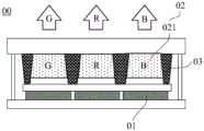
图1示出了相关技术中的显示装置00。如图1所示,该显示装置00包括多个发蓝光的发光部01、以及设置于该多个发蓝光的发光部01出光侧的彩色滤光层02和遮光图案03。其中,彩色滤光层02包括多个滤光部021(例如绿色滤光部、红色滤光部、蓝色滤光部),多个滤光部021与多个发蓝光的发光部01一一对应设置(即,一个发蓝光的发光部01和一个滤光部021位于同一个子像素内),多个滤光部021用于对进入其内的蓝色光线进行过滤,以使用于色彩显示的三基色光线透过(例如绿色滤光部仅可以透过绿色光线、红色滤光部仅可以透过红色光线、蓝色滤光部仅可以透过蓝色光线),从而实现全彩显示;遮光图案03设置在任意相邻滤光部021之间,遮光图案03具有吸收所有可见波段的光线的作用,用于将各个滤光部021隔开,防止不同的滤光部021之间发生串色,影响显示效果。FIG. 1 shows a
然而,在上述显示装置00中,经红色滤光部出射的红色光线的亮度以及经绿色滤光部出射的绿色光线的亮度都比较低,经蓝色滤光部出射的蓝色光线的亮度比较高。也即,该显示装置00存在红色子像素和绿色子像素出光亮度低,而蓝色子像素的出光亮度高的问题,进而导致该显示装置00在显示白画面时功耗会比较高。However, in the above-mentioned
基于此,本公开一些实施例提供一种显示面板。如图2所示,该显示面板1包括至少一个像素单元10,像素单元10包括第一子像素11、第二子像素12、第三子像素13和第四子像素14。Based on this, some embodiments of the present disclosure provide a display panel. As shown in FIG. 2 , the
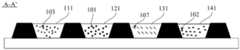
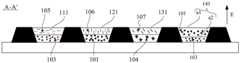
如图2所示,该第一子像素11包括第一彩膜部111,第一彩膜部111被配置为出射第一颜色光线(例如图2示出的第一彩膜部111被配置为出射红色光线);该第二子像素12包括第二彩膜部121,第二彩膜部121被配置为出射第二颜色光线(例如图2示出的第二彩膜部121被配置为出射绿色光线);该第三子像素13包括第三彩膜部131,第三彩膜部131被配置为出射第三颜色光线(例如图2示出的第三彩膜部111被配置为出射红色光线);其中,第三颜色光线与第一颜色光线、第二颜色光线为三基色光线。此处需要说明的是,图2仅是本公开的一种示例,而非对本公开实施例的限制。本公开实施例中的第一彩膜部111、第二彩膜部121和第三彩膜部131只需要满足能够出射三基色光线即可。例如,该三基色光线可以是红色光线、绿色光线和蓝色光线;又例如,该三基色光线还可以是红色光线、黄色光线和蓝色光线。As shown in FIG. 2 , the
如图2、图3A~图3D所示,该第四子像素14包括第四彩膜部141,第四彩膜部141包括至少一种光转换材料,所述至少一种光转换材料被配置为将射向所述第四彩膜部141的一部分光线转换为至少一种基色光线,所述至少一种基色光线能够与射向该第四彩膜部141的另一部分光线混合以出射白色光线。As shown in FIGS. 2 and 3A to 3D , the
例如,在射向该第四彩膜部141的光线为蓝色光线和红色光线时,该第四彩膜部141中的光转换材料(如图3A示出的绿光转换材料101)可以将蓝色光线中的一部分转换为绿色光线,然后使转换得到的绿色光线与射向该第四彩膜部141的红色光线、以及该蓝色光线中的另一部分混合,从而达到出射白色光线的目的;又例如,在射向该第四彩膜部141的光线为蓝色光线和红色光线时,该第四彩膜部141中的光转换材料(如图3B示出的黄光转换材料102)可以将蓝色光线中的一部分转换为黄色光线,然后使转换得到的黄色光线与射向该第四彩膜部141的红色光线、以及该蓝色光线中的另一部分混合,从而达到出射白色光线的目的;又例如,在射向该第四彩膜部141的光线为蓝色光线时,该第四彩膜部141中的光转换材料(如图3C示出的绿光转换材料101和红光转换材料103)可以将蓝色光线中的一部分转换为绿色光线和红色光线,然后使转换得到的绿色光线和红色光线与该蓝色光线中的另一部分混合,从而达到出射白色光线的目。For example, when the light emitted to the fourth
其中,需要说明的是,该第四彩膜部141中的光转换材料,可以是将短波长光线转换为长波长光线(例如将蓝色光线转换为绿色光线)的光转换材料,也可以是将长波长光线转换为短波长光线(例如将红色光线转换为绿色光线)的光转换材料。本公开实施例对此不做限制,只需要满足转换后得到的光线能够与未被转换的光线混合形成白色光线即可。It should be noted that the light conversion material in the fourth
本公开实施例提供的显示面板中,由于设置有可以出射白色光线的第四子像素,因此只需控制对应的第四子像素发光即可实现白画面显示,而无需通过第一子像素(例如红色子像素)、第二子像素(例如绿色子像素)和第三子像素(例如蓝色子像素)同时发光来输出白光以显示白画面。从而不会因红色子像素和绿色子像素出光亮度低,蓝色子像素的出光亮度高,而导致显示面板在显示白画面时功耗较高。换言之,采用该显示面板的显示装置在显示白画面时,相较相关技术中的显示装置而言,具有功耗更低的优点,而且在此基础上,还有利于进一步提高该显示装置的使用寿命。In the display panel provided by the embodiments of the present disclosure, since the fourth sub-pixels that can emit white light are provided, white screen display can be realized only by controlling the corresponding fourth sub-pixels to emit light without passing the first sub-pixels (for example, A red sub-pixel), a second sub-pixel (eg, a green sub-pixel), and a third sub-pixel (eg, a blue sub-pixel) simultaneously emit light to output white light to display a white picture. Therefore, the red sub-pixels and the green sub-pixels have low light-emitting brightness, and the blue sub-pixels have high light-emitting brightness, resulting in high power consumption of the display panel when displaying a white image. In other words, the display device using the display panel has the advantage of lower power consumption compared to the display device in the related art when displaying a white picture, and on this basis, it is also beneficial to further improve the use of the display device life.
示例性的,参见图3A~图3D,该第四彩膜部141中的光转换材料包括绿光转换材料101、黄光转换材料102和红光转换材料103中的至少一者。其中,该绿光转换材料101被配置为将接收到的光线转换为绿色光线;该黄光转换材料102被配置为将接收到的光线转换为黄色光线;该红光转换材料103被配置为将接收到的光线转换为红色光线。Exemplarily, referring to FIGS. 3A to 3D , the light conversion material in the fourth
在该第四彩膜部141包括绿光转换材料101和红光转换材料103的情况下:如图3C所示,该第四彩膜部141中红光转换材料103的掺杂质量百分比约为该第四彩膜部141中绿光转换材料101的掺杂质量百分比的0.5倍(其中,“约”是指在0.5倍的基础上可以上下浮动,例如在实际应用中也可以为0.4~0.6倍);和/或,如图3D所示,该第四彩膜部141包括沿由该第四彩膜部141的入光侧指向该第四彩膜部的出光侧的方向E依次层叠设置第一膜层a1和第二膜层a2,其中,该第一膜层a1中设置有红光转换材料103,该第二膜层a2中设置有绿光转换材料101。In the case where the fourth
本实施例中,通过设置该第四彩膜部141中红光转换材料103的掺杂质量百分比约为该第四彩膜部141中绿光转换材料101的掺杂质量百分比的0.5倍,使得经该第四彩膜部141后转换得到的红色光线的强度小于经该第四彩膜部141后转换得到的绿色光线的强度。而通过设置第一膜层a1和第二膜层a2,并在第一膜层a1中设置红光转换材料103,在第二膜层a2中设置有绿光转换材料101,可以使红光转换材料起到充分的光转换作用。这样设计,有利于提高混合后形成的白色光线的纯度,进而有利于提高显示装置的白画面显示效果。In this embodiment, the doping mass percentage of the red
需要说明的是,在该第四彩膜部141中红光转换材料103的掺杂质量百分比约为该第四彩膜部141中绿光转换材料101的掺杂质量百分比的0.5倍的情况下,这两种材料可以如图3C所示直接混合掺杂,或者,也可以如图3D所示分别掺杂在第一膜层a1和第二膜层a2中。而在图3D示出的基础上,示例性的,可以设置该第一膜层a1的厚度约为该第二膜层a2的厚度的0.5倍(其中,“约”是指在0.5倍的基础上可以上下浮动,例如在实际应用中也可以为0.4~0.6倍);此时,可以使红光转换材料103在第一膜层a1中的掺杂质量百分比接近绿光转换材料101在第二膜层a2中的掺杂质量百分比,进而更有利于提高光线在第一膜层a1和第二膜层a2中的转换效果。It should be noted that when the doping mass percentage of the red
在一些实施例中,该第四彩膜部141中光转换材料(即该第四彩膜部141中的全部光转换材料,例如包括绿光转换材料、黄光转换材料和红光转换材料中的至少一者)的掺杂质量百分比为15%~90%。例如可以为50%~75%,又例如可以为70%。这样设计,使得射向该第四彩膜部141的光线不会完全被该第四彩膜部141中的光转换材料吸收并转换,进而可以使该第四彩膜部141中转换得到的光线与未被转换的光线混合以实现输出白色光线。In some embodiments, the light conversion material in the fourth color filter portion 141 (that is, all the light conversion materials in the fourth
对于上述第一彩膜部111、第二彩膜部121以及第三彩膜部131中的任一者,可以按照以下一些示例进行设置。For any one of the first
示例性的,如图3A~图3D所示,该第一彩膜部111包括红光转换材料103,或者,该第一彩膜部111包括同时红色滤光材料105和红光转换材料103。该红色滤光材料105被配置为仅透过红色光线,该红光转换材料103被配置为将接收到的光线转换为红色光线。也即,该第一彩膜部111可以如图3A和图3B所示仅包括红光转换材料103,或者,也可以如图3C和图3D所示同时包括红色滤光材料105和红光转换材料103。而且,在该第一彩膜部111同时包括红色滤光材料105和红光转换材料103的情况下,这两种材料可以如图3C所示直接混合掺杂,或者也可以如图3D所示设置该第一彩膜部111中包含红色滤光材料105的部分位于包含红光转换材料103的部分的出光侧。这样设计,使得在射向该第一彩膜部111的光线未被包含红光转换材料103的部分完全转换时,可以利于包含红色滤光材料105的部分对未被转换的光线进行过滤,进而可以防止该第一彩膜部111出射不希望出现的颜色光线,也即使得该第一彩膜部可以出射纯度较高的出射红色光线。Exemplarily, as shown in FIGS. 3A to 3D , the first
示例性的,如图3A~图3D所示,该第二彩膜部121包括绿光转换材料101,或者,该第二彩膜部121同时包括绿色滤光材料106和绿光转换材料101。该绿色滤光材料106被配置为仅透过绿色光线,该绿光转换材料101被配置为将接收到的光线转换为绿色光线。也即,该第二彩膜部121可以如图3A和图3B所示仅包括绿光转换材料101,或者,也可以如图3C和图3D所示同时包括绿色滤光材料106和绿光转换材料101。而且,在该第二彩膜部121同时包括绿色滤光材料106和绿光转换材料101的情况下,这两种材料可以如图3C所示直接混合掺杂,或者也可以如图3D所示设置第二彩膜部121中包含绿色滤光材料106的部分位于包含绿光转换材料101的部分的出光侧。这样设计,使得在射向该第二彩膜部121的光线未被包含绿光转换材料101的部分完全转换时,可以利于包含绿色滤光材料106的部分对未被转换的光线进行过滤,进而可以防止该第二彩膜部121出射不希望出现的颜色光线,也即使得该第二彩膜部121可以出射纯度较高的出射绿色光线。Exemplarily, as shown in FIGS. 3A to 3D , the second
示例性的,如图3A~图3D所示,该第三彩膜部131包括蓝色滤光材料107和/或蓝光转换材料104,该蓝色滤光材料107被配置为仅透过蓝色光线,该蓝光转换材料104被配置为将接收到的光转换为蓝光。也即,该第三彩膜部131可以如图3A所示仅包括蓝光转换材料104,可以如图3B所示仅包括蓝色滤光材料107,或者,也可以如图3C和图3D所示同时包括蓝色滤光材料107和蓝光转换材料104。而且,在该第三彩膜部131同时包括蓝色滤光材料107和蓝光转换材料104的情况下,这两种材料可以如图3C所示直接混合掺杂,或者也可以如图3D所示设置第三彩膜部131中包含蓝色滤光材料107的部分位于包含蓝光转换材料104的部分的出光侧。这样设计,使得在射向该第三彩膜部131的光线未被包含蓝光转换材料104的部分完全转换时,可以利于包含蓝色滤光材料107的部分对未被转换的光线进行过滤,进而可以防止该第三彩膜部131出射不希望出现的颜色光线,也即使得该第三彩膜部131可以出射纯度较高的出射蓝色光线。Exemplarily, as shown in FIGS. 3A to 3D , the third
其中,上述红色滤光材料105、绿色滤光材料106和蓝色滤光材料107可以为光阻材料;上述绿光转换材料101、黄光转换材料102、红光转换材料103和蓝光转换材料104可以为荧光材料或量子点材料。Wherein, the
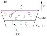
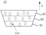
在一些实施例中,如图2、图4A~图4C所示,该第一彩膜部111、该第二彩膜部121、该第三彩膜部131和该第四彩膜部141中的至少一者还包括散射材料151。下面为了方便说明,以彩膜部15表示第一彩膜部111、第二彩膜部121、第三彩膜部131和第四彩膜部141中的一者,如图4A~图4C所示,该彩膜部15中包括散射材料151,例如该散射材料151可以是分散剂或者散射粒子。在该散射材料151为散射粒子的情况下,可以通过该散射粒子使光线在彩膜部15内来回反射,以提高光转换材料对光线的吸收转换效率。而在该散射材料151为分散剂的情况下,分散剂自身可以作为具有反射作用的粒子,而且通过分散剂还能够分散该彩膜部15中固体或液体粒子聚集的物质,此时,通过分散剂自身以及通过分散剂分散聚积物质得到的粒子可以使光线在彩膜部15内来回反射,进而可以大幅提高光转换材料对光线的吸收转换效率。In some embodiments, as shown in FIG. 2 and FIG. 4A to FIG. 4C , the first
示例性的,该散射材料151的粒径为5nm~1000nm。例如,该散射材料151的粒径可以为50nm~200nm,又例如,该散射材料151的粒径可以为5nm、50nm、100nm、200nm或者1000nm等。这样光线在彩膜部15中的散射效果会比较好。Exemplarily, the particle size of the
又示例性的,该彩膜部15中该散射材料151的掺杂质量百分比为0.01%~50%。例如,可以为3%~25%,又例如可以为3%、5%、25%。这样设计,既可以通过散射材料151提高光线散射效果,又不会因散射材料151掺杂过多而导致影响彩膜部15的透过率。In another example, the doping mass percentage of the
在一些示例中,如图4B和图4C所示,该散射材料151所在的彩膜部15包括沿第一方向E依次层叠设置的至少两层散射层;该第一方向E由该彩膜部15的入光侧指向该彩膜部15的出光侧,例如图3D中该第一方向E可以是由第四彩膜部141的入光侧指向该第四彩膜部141的出光侧。In some examples, as shown in FIGS. 4B and 4C , the
相邻两层散射层中,靠近该彩膜部15的出光侧的散射层(如图4B中的第二散射层b2)中该散射材料的掺杂质量百分比大于靠近该彩膜部15的入光侧的散射层(如图4B中的第一散射层b1)中该散射材料的掺杂质量百分比。这样可使更多光线进入彩膜部15,并提高光线被彩膜部15中光转换材料吸收及转换的效率。Among the two adjacent scattering layers, the scattering layer near the light-emitting side of the color filter portion 15 (as shown in the second scattering layer b2 in FIG. 4B ) has a higher doping mass percentage of the scattering material than that near the
其中,各散射层的厚度(即沿第一方向E的尺寸)的取值范围可以为0.1μm~20μm。Wherein, the thickness of each scattering layer (that is, the dimension along the first direction E) may range from 0.1 μm to 20 μm.
示例性的,如图4B所示,该散射材料151所在的彩膜部15包括沿第一方向E依次层叠设置的第一散射层b1和第二散射层b2;该第一散射层b1的厚度约为4μm,该第一散射层b1中散射材料151的掺杂质量百分比约为5%;该第二散射层b2的厚度约为6μm,该第二散射层b2中散射材料151的掺杂质量百分比约25%。其中“约”是指在对应数值的基础上可以上下浮动百分之十,例如第一散射层b1的厚度约为4μm,可以是指该第一散射层c1的厚度取值范围为3.6μm~4.4μm。本示例中的彩膜部15可以吸收更多光线,并且可以提高光线被光转换材料转换的效率。Exemplarily, as shown in FIG. 4B , the
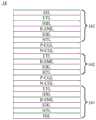
或者,如图4C所示,该散射材料151所在的彩膜部15包括沿第一方向E依次层叠设置的第一散射层b1、第二散射层b2和第三散射层b3;该第一散射层b1的厚度约为3μm,该第一散射层b1中散射材料151的掺杂质量百分比约为3%;该第二散射层b2的厚度约为3μm,该第二散射层b2中散射材料151的掺杂质量百分比约为12%;该第三散射层b3的厚度约为3μm,该第三散射层b3中散射材料151的掺杂质量百分比约为25%。其中“约”是指在各对应数值的基础上可以上下浮动百分之十,例如第一散射层b1的厚度约为3μm,可以是指该第一散射层b1的厚度取值范围为2.7μm~3.3μm。本示例中的彩膜部15可以吸收更多光线,并且可以提高光线被光转换材料转换的效率。Alternatively, as shown in FIG. 4C , the
其中,在第一彩膜部111按照散射材料151的掺杂量不同分为上述第一散射层b1和第二散射层b2,且该第一彩膜部111同时包括红光转换材料103和红色滤光材料105的情况下,如图4D和图4E所示,可以设置红光转换材料103掺杂于第一散射层b1中,红色滤光材料105掺杂于第二散射层b2中。即,此时该第一彩膜部111中包含红光转换材料103的部分为第一散射层b1,该第一彩膜部111中包含红色滤光材料105的部分为第二散射层b2。而在第一彩膜部111按照散射材料151的掺杂质量百分比分为上述第一散射层b1、第二散射层b2和第三散射层b3,且该第一彩膜部111同时包括红光转换材料103和红色滤光材料105的情况下,如图4F和图4G所示,可以设置该红光转换材料103掺杂于第一散射层b1和第二散射层b2中,红色滤光材料105掺杂于第三散射层b3中。即,此时该第一彩膜部111中包含红光转换材料103的部分为第一散射层b1和第二散射层b2,该第一彩膜部111中包含红色滤光材料105的部分为第三散射层b3。The first
在第二彩膜部121按照散射材料151的掺杂量不同分为上述第一散射层b1和第二散射层b2,且该第二彩膜部121同时包括绿光转换材料101和绿色滤光材料106的情况下,如图4D和图4E所示,可以设置绿光转换材料101掺杂于第一散射层b1中,绿色滤光材料106掺杂于第二散射层b2中。即,此时该第二彩膜部121中包含绿光转换材料101的部分为第一散射层b1,该第二彩膜部121中包含绿色滤光材料106的部分为第二散射层b2。而在第二彩膜部121按照散射材料151的掺杂质量百分比分为上述第一散射层b1、第二散射层b2和第三散射层b3,且该第二彩膜部121同时包括绿光转换材料101和绿色滤光材料106的情况下,如图4F和图4G所示,可以设置该绿光转换材料101掺杂于第一散射层b1和第二散射层b2中,绿色滤光材料106掺杂于第三散射层b3中。即,此时该第二彩膜部121中包含绿光转换材料101的部分为第一散射层b1和第二散射层b2,该第二彩膜部121中包含绿色滤光材料106的部分为第三散射层b3。The second
在第三彩膜部131按照散射材料151的掺杂量不同分为上述第一散射层b1和第二散射层b2,且该第三彩膜部131同时包括蓝光转换材料104和蓝色滤光材料107的情况下,如图4D所示,可以设置蓝光转换材料104掺杂于第一散射层b1中,蓝色滤光材料107掺杂于第二散射层b2中。即,此时该第三彩膜部131中包含蓝光转换材料104的部分为第一散射层b1,该第三彩膜部131中包含蓝色滤光材料107的部分为第二散射层b2。而在第三彩膜部131按照散射材料151的掺杂质量百分比分为上述第一散射层b1、第二散射层b2和第三散射层b3,且该第三彩膜部131同时包括蓝光转换材料104和蓝色滤光材料107的情况下,如图4F所示,可以设置该蓝光转换材料104掺杂于第一散射层b1和第二散射层b2中,蓝色滤光材料107掺杂于第三散射层b3中。即,此时该第三彩膜部131中包含蓝光转换材料104的部分为第一散射层b1和第二散射层b2,该第三彩膜部131中包含蓝色滤光材料107的部分为第三散射层b3。The third
此处,需要说明的是,由于射向该第三彩膜部131的光线通常至少包括蓝色光线,因此,如图4E和4G所示,该第三彩膜部131可以仅包括蓝色滤光材料107。而且,此时该第三彩膜部131中既可以不设置散射材料151,也可以设置多层散射材料。Here, it should be noted that, since the light entering the third
而在第四彩膜部141按照散射材料151的掺杂量不同分为上述第一散射层b1和第二散射层b2的情况下,如图4D~图4G所示,该第一散射层b1与该第四彩膜部141的第二膜层a2可以是该第四彩膜部141的同一部分,该第二散射层b2与该第四彩膜部141的第一膜层a1可以是该第四彩膜部141的同一部分。可以理解的是,本公开实施例并不对此进行限制,例如在另一些示例中,该第四彩膜层141中第一散射层b1和第二散射层b2的分界线,也可以与第四彩膜层中第一膜层a1和第二膜层a2的分界线不重合。又例如,在又一些示例中,该第四彩膜部141按照散射材料151的掺杂量不同还可以分为第一散射层b1和第二散射层b2和第三散射层b3。这三个散射层组成的整个第四彩膜部141同样可以按照所包含的光转换材料不同分为第一膜层a1和第二膜层a2。In the case where the fourth
需要说明的是,上述各实施例所描述的显示面板1,可以是图5A示出的对盒式显示面板(即彩膜基板1A与显示基板2A对盒设置,并通过封框胶51连接形成的显示面板),也可以是图5B示出的第二种显示面板(即在设置有驱动电路及发光部的衬底上直接制作有彩膜的显示面板)。在该显示面板1为对盒式显示面板的情况下,如图5A所示,该彩膜基板1A可以与未设置彩膜的显示基板2A对盒安装,从而实现全彩显示。其中,彩膜基板1A除包括第一彩膜部111、第二彩膜部121、第三彩膜部131和第四彩膜部141外,还包括用于将相邻的彩膜部(例如图5A示出的第一彩膜部111和第二彩膜部121、第二彩膜部121和第三彩膜部131、以及第三彩膜部131和第四彩膜部141)间隔开的间隔图案17,该间隔图案17可以防止不同的彩膜部之间发生串色,从而提高显示效果。同时,该间隔图案17可以具有吸光和/或反射光的功能,并且该间隔图案17还可以是透明的。在此基础上,可以设置间隔图案17靠近各彩膜部(例如第一彩膜部111、第二彩膜部121、第三彩膜部131和第四彩膜部141)的侧面具有反射光的功能(可以理解,在该间隔图案透明的情况下,可以通过在该侧面涂覆反射材料,从而实现反射光的功能),这样可以将光线更好的限制在各彩膜部中,从而有利于进一步提高各彩膜部的出光亮度。It should be noted that the
在此基础上,该显示面板1中的彩膜基板1A包括第一衬底100,该第一衬底100用于承载多个彩膜部(例如第一彩膜部111、第二彩膜部121、第三彩膜部131和第四彩膜部141)以及间隔图案17。同时,在形成有多个彩膜部及间隔图案17的第一衬底100上还可以形成有第一封装层18,通过设置该第一封装层18可以避免第一彩膜部111、第二彩膜部121、第三彩膜部131和第四彩膜部141受到水氧侵害。On this basis, the
继续参见图5A,该显示面板1中的显示基板2A包括第二衬底200,以及依次设置于该第二衬底200上的驱动电路、发光器件和第二封装层25。其中,驱动电路包括多个薄膜晶体管21。发光器件包括阳极22、发光部16以及阴极24,阳极22和多个薄膜晶体管21中作为驱动晶体管的薄膜晶体管21的漏极电连接。该未设置彩膜的显示基板2A还包括像素界定层23,像素界定层23包括多个开口区,一个发光部16设置在一个开口区中。Continuing to refer to FIG. 5A , the
示例性的,如图5A所示,在该显示面板1中,彩膜基板1A与显示基板2A对盒安装时,还可以在两者之间设置填充层,例如该填充层可以包括层叠设置的有机膜层31、无机膜层32和有机膜层33,这样有利于提高两者对盒安装后的稳定性和可靠性,使显示面板1不易发生变形。此外,还可以在整体的侧面设置一圈封框胶51(如图5A和图7A所示),例如,该封框胶51可以是紫外光(Ultraviolet Rays,UV)固化胶,这样有利于防止水汽渗入,提高使用寿命。Exemplarily, as shown in FIG. 5A , in the
在该彩膜基板1A与显示基板2A对盒安装后,示例性的,如图5A所示,该间隔图案17靠近第二衬底200的表面与第二衬底200之间的距离L1小于该彩膜部靠近第二衬底200的表面与第二衬底200之间的距离L2。这样可以更好的避免多个滤光部之间发生串色。After the
在该彩膜基板1A与显示基板2A对盒后,各发光部16位于与其对应的彩膜部的入光侧,例如在图5A中,显示基板2A包括设置于第一彩膜部111入光侧的发光部16、设置于第二彩膜部121入光侧的发光部16、设置于第三彩膜部131入光侧的发光部16、以及设置于第四彩膜部141入光侧的发光部16。After the
而在该显示面板1为如上所述的第二种显示面板的情况下,如图5B所示,该第二种显示面板包括第二衬底200,该第二衬底200上设置有多个彩膜部(例如所述第一彩膜部111、第二彩膜部121、第三彩膜部131和第四彩膜部141)。在此基础上,如图5B所示,该第二种显示面板还包括多个发光部16,各发光部16位于一个彩膜部与第二衬底200之间。例如,在图5B中,该第二种显示面板设置于该第一彩膜部111入光侧的发光部16、设置于该第二彩膜部121入光侧的发光部16、设置于该第三彩膜部131入光侧的发光部16、和设置于该第四彩膜部141入光侧的发光部16。In the case where the
在该第二种显示面板中,示例性的,如图5B所示,还包括设置于第二衬底200上的间隔图案17(该间隔图案17可以与上述彩膜基板1A中的间隔图案7相同,此处不再赘述),并且该间隔图案17靠近第二衬底200的表面与彩膜部靠近第二衬底200的表面齐平。这样可以更好的避免多个滤光部之间发生串色。In the second type of display panel, exemplary, as shown in FIG. 5B , further includes a spacer pattern 17 (the
参见图5A和图5B,该第二种显示面板与未设置彩膜的显示基板2A之间的区别在于,该第二种显示面板在制备完覆盖阴极层24的第二封装层25之后,依次形成一层有机膜层26和一层无机膜层27,该无机膜层27的远离第二衬底200的表面为平面,因此便于在该无机膜层27上继续制备上述间隔图案17、以及多个彩膜部(例如第一彩膜部111、第二彩膜部121、第三彩膜部131和第四彩膜部141)。最后还可以形成覆盖彩膜部及间隔图案17的第一封装层18,通过设置该封装层18可以避免第一彩膜部111、第二彩膜部121、第三彩膜部131和第四彩膜部141受到水氧侵害。Referring to FIGS. 5A and 5B , the difference between the second type of display panel and the
示例性的,该上述第一封装层18和第二封装层25均可以设置为包括依次层叠设置的无机膜层、有机膜层和无机膜层的三层结构,这样有利于提高封装效果。Exemplarily, the above-mentioned
在上述任意一种显示面板的基础上,在一些实施例中,上述发光部16包括层叠设置的至少一组发红光的发光功能层162和至少一组发蓝光的发光功能层161。Based on any of the above-mentioned display panels, in some embodiments, the light-emitting
例如,如图6所示,该发光部16包括两组发蓝光的发光功能层161,以及设置于这两组发蓝光的发光功能层161之间的一组发红光的发光功能层162。在此基础上,如图6所示,相邻的两组发光功能层之间可以通过P型电荷产生层P-CGL和N型电荷产生层N-CGL连接。也即,该发光部16可以包括依次层叠设置的电子注入层EIL、电子传输层ETL、空穴阻挡层HBL、蓝色发光层B-EML、电子阻挡层EBL、空穴传输层HTL、P型电荷产生层P-CGL、N型电荷产生层N-CGL、电子传输层ETL、红色发光层R-EML、电子阻挡层EBL、空穴传输层HTL、P型电荷产生层P-CGL、N型电荷产生层N-CGL、电子传输层ETL、空穴阻挡层HBL、蓝色发光层B-EML、电子阻挡层EBL、空穴传输层HTL、空穴注入层HIL。其中,P型电荷产生层P-CGL和N型电荷产生层N-CGL在外加电场条件下能够产生电子和空穴,从而能够提高位于中间的发光功能层的发光效果,并且有利于提高该发光部16的发光稳定性。For example, as shown in FIG. 6 , the light-emitting
该发光部16可以同时出射蓝色光线和红色光线,且蓝色光线的强度比较强。在将该发光部16设置于第四彩膜部141的入光侧时,该第四彩膜部141中的光转换材料(如图3A示出的绿光转换材料101)可以将蓝色光线中的一部分转换为绿色光线,然后使转换得到的绿色光线与射向该第四彩膜部141的红色光线、以及该蓝色光线中的另一部分混合,从而达到出射白色光线的目的,并且该白色光线的纯度和亮度较高。The light-emitting
需要说明的是,本公开实施例中的发光部16不局限于上述结构,只要能够满足发光部16与第四彩膜部141配合实现出射白色光线即可。例如,在上述结构的基础上,可以减少一组发蓝光的发光功能层161,也可以再增加一组发蓝光的发光功能层161,此时,均有利于提高混合形成的白色光线的纯度和亮度。又例如,该发光部16还可以仅设置一组或多组发蓝光的发光功能层161,此时仍然能够与第四彩膜部141(此时该第四彩膜部同时包括绿光转换材料和红光转换材料)配合实现出射白色光线。It should be noted that, the light-emitting
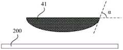
在一些实施例中,如图7A和图7B所示,该显示面板1还包括调光透镜41,该调光透镜41设置于发光部16和与该发光部16对应的彩膜部之间。例如,各发光部16和与该发光部对应的彩膜部之间设置有一个或多个调光透镜41,此时,可以利用位于一个发光部16和与该发光部对应的彩膜部之间的一个或多个调光透镜41,收敛由该发光部16发出的光线,以使该发光部16发出的光线能够射向对应的彩膜部。其中,在位于一个发光部16和与该发光部对应的彩膜部之间的调光透镜41的数量为一个的情况下(例如图7A和图7B中,在第一彩膜部111、第二彩膜部121、第三彩膜部131和第四彩膜部141四者的入光侧分别设置有一个调光透镜41),该发光部16在参考平面M(即平行于第二衬底200的平面)的正投影和与其对应的彩膜部在该参考平面M上的正投影均位于该一个调光透镜41在该参考平面M的正投影范围之内,这样可以更好的收敛由该发光部16发出的光线,以使该发光部16发出的光线能够射向对应的彩膜部。而在位于一个发光部16和与该发光部对应的彩膜部之间的调光透镜41的数量为多个的情况下,如图7C和图7D所示,可以将该多个调光透镜41阵列排布,以利用该多个调光透镜41收敛由该发光部16发出的光线,以使该发光部16发出的光线能够射向对应的彩膜部。同时,该发光部16在该参考平面M的正投影和与其对应的彩膜部在该参考平面M上的正投影均位于该多个调光透镜41在该参考平面M的正投影范围之内。In some embodiments, as shown in FIGS. 7A and 7B , the
又例如,该调光透镜41呈条状,同一行或者同一列的多个发光部16在参考平面上的正投影处于一个调光透镜41在所述参考平面M上的正投影范围之内,该参考平面平行于第二衬底200。此时,可以利用一个调光透镜对同一行或者同一列的多个发光部16发出的光线进行收敛,以使各发光部16发出的光线可以更多的射向与其对应的彩膜部,从而有利于提高显示亮度。For another example, the dimming
需要说明的是,上述位于正投影范围之内,是指包括两个正投影彼此重叠的情况。而且示例性的,可以设置调光透镜41在参考平面的正投影边缘超出位于其正投影范围之内的发光部和/或彩膜部的正投影边缘2μm~5μm。这样使其下方的发光部16发出的光线更多地被搜集会聚至其上方的彩膜部中。It should be noted that the above-mentioned being within the orthographic projection range refers to the case where two orthographic projections overlap each other. Also exemplarily, the orthographic projection edge of the dimming
示例性的,如图7A和图7B所示,该调光透镜41的靠近发光部16的表面为凸面;并且该调光透镜41的靠近彩膜部的表面为平面或凹面。这样能够达到较好的光线收敛效果。Exemplarily, as shown in FIG. 7A and FIG. 7B , the surface of the dimming
图7E和图7F中示出了两种调光透镜41的截面示意图。示例性的,如图7E所示,该调光透镜41为平凸透镜,此时,该调光透镜41的平面可以平行于该第二衬底200,并且过该调光透镜41的凸面边缘上的任一点且与该凸面相切的切线与平行于第二衬底200的平面之间的夹角α可以为20°~80°,这样具有更好的聚光效果。又示例性的,如图7F所示,该调光透镜41可以为凹凸透镜,此时过该调光透镜41的凸面边缘上的任一点且与该凸面相切的切线与平行于第二衬底200的平面之间的夹角α可以为20°~80°,这样具有更好的聚光效果。Two schematic cross-sectional views of the dimming
在一些实施例中,该显示面板1还包括第一填充层34和第二填充层35。该第一填充层34设置于调光透镜41与发光部16之间,该第二填充层35设置于调光透镜41与彩膜部(例如第一~第四彩膜部)之间。该调光透镜41的折射率大于第一填充层34的折射率,并且调光透镜41的折射率小于或等于第二填充层35的折射率。这样设计使得由发光部16射向对应的彩膜部的光线,在依次经过第一填充层34、调光透镜41和第二填充层35时,不会发光全反射,进而能够保证更多的光线射线彩膜部。In some embodiments, the
其中,该第一填充层34、调光透镜41和第二填充层35均可以由树脂(resin)材料制作,只要保证三者的折射率满足上述要求即可。另外,对于各调光透镜41沿垂直于参考平面M方向的厚度,可以根据所要达到的光线收敛程度进行设置,本公开实施例并非对此进行限制。The
本公开一些实施例还提供一种显示装置300,如图8所示,该显示装置300包括上述任一实施例所述的显示面板。其中,该显示装置300例如可以是该显示装置20例如可以是电视、数码相机、手机、手表、平板电脑、笔记本电脑、导航仪等任何适当的部件。该显示装置的技术效果,可参见上述实施例描述的显示面板的技术效果,在此不再赘述。Some embodiments of the present disclosure further provide a
本公开的一些实施例还提供了一种显示面板的制作方法,如图9所示,该制作方法包括步骤S1。Some embodiments of the present disclosure also provide a manufacturing method of a display panel, as shown in FIG. 9 , the manufacturing method includes step S1 .
步骤S1、参见图5A,在衬底(如第一衬底100)上形成至少一个像素单元,像素单元包括第一子像素11、第二子像素12、第三子像素13和第四子像素14;第一子像素11包括第一彩膜部111,第二子像素12包括第二彩膜部121,第三子像素13包括第三彩膜部131,第四子像素14包括第四彩膜部141。其中,该第一衬底100例如可以是玻璃基板、石英基板、塑料基板或其它适合材料的基板。例如,在一个示例中,第一衬底100还可以是柔性衬底基板,该柔性衬底基板例如是透明基板且可以弯曲。Step S1, referring to FIG. 5A, at least one pixel unit is formed on a substrate (eg, the first substrate 100), and the pixel unit includes a
该第一彩膜部111被配置为出射第一颜色光线;该第二彩膜部121被配置为出射第二颜色光线;该第三彩膜部131被配置为出射第三颜色光线;第三颜色光线与第一颜色光线、第二颜色光线为三基色光线。该第四彩膜部141包括至少一种光转换材料,所述至少一种光转换材料配置为将射向所述第四彩膜部141的一部分光线转换为至少一种基色光线,所述至少一种基色光线能够与射向该第四彩膜部141的另一部分光线混合以出射白色光线。The first
通过步骤S1形成的显示面板,由于设置有可以出射白色光线的第四子像素14,因此只需控制对应的第四子像素14发光即可实现白画面显示,而无需通过第一子像素11(例如红色子像素)、第二子像素12(例如绿色子像素)和第三子像素13(例如蓝色子像素)同时发光来输出白光以显示白画面。从而不会因红色子像素和绿色子像素出光亮度低,蓝色子像素的出光亮度高,而导致显示装置在显示白画面时功耗较高。换言之,采用该显示面板的显示装置在显示白画面时,相较相关技术中的显示装置而言,具有功耗更低的优点,而且在此基础上,还有利于进一步提高该显示装置的使用寿命。Since the display panel formed by step S1 is provided with the fourth sub-pixels 14 that can emit white light, it is only necessary to control the corresponding fourth sub-pixels 14 to emit light to achieve white screen display, without the need for the first sub-pixels 11 ( For example, a red sub-pixel), a second sub-pixel 12 (for example, a green sub-pixel), and a third sub-pixel 13 (for example, a blue sub-pixel) simultaneously emit light to output white light to display a white picture. Therefore, the red sub-pixels and the green sub-pixels have low light-emitting brightness, and the blue sub-pixels have high light-emitting brightness, resulting in high power consumption of the display device when displaying a white image. In other words, the display device using the display panel has the advantage of lower power consumption compared to the display device in the related art when displaying a white picture, and on this basis, it is also beneficial to further improve the use of the display device life.
在此基础上,还可以包括步骤S2、参见图7A,在形成有第一彩膜部111、第二彩膜部121、第三彩膜部131和第四彩膜部141的衬底(即第一衬底100)上依次形成第二填充层35、透镜层和第一填充层34;透镜层包括至少一个调光透镜41。On this basis, step S2 may also be included. Referring to FIG. 7A , in the substrate (ie The
其中,各调光透镜41覆盖至少一个彩膜部,各调光透镜41的靠近所述至少一个彩膜部的表面为平面或凹面,各调光透镜41的远离所述至少一个彩膜部的表面为凸面。并且各调光透镜41的折射率大于第一填充层34的折射率,各调光透镜41的折射率小于或等于第二填充层35的折射率。Wherein, each dimming
示例性的,各调光透镜41的折射率与第一填充层34的折射率之差大于或等于0.2。例如,可以设置该第一填充层34的材料为树脂材料,折射率范围为1.0~2.0,比如1.4~1.6;对应的,可以设置调光透镜41的材料为树脂材料,折射率范围为1.0~2.3,比如1.6~1.8。Exemplarily, the difference between the refractive index of each dimming
参见图7A,在制作该显示面板时,可以先在第一封装层18上涂覆形成第二填充层35的材料,并进行后烘固化形成第二填充层35;然后在第二填充层35和第一封装层18上形成包括至少一个调光透镜41的透镜层;最后形成覆盖透镜层的第一填充层34。Referring to FIG. 7A , when manufacturing the display panel, a material for forming the
通过步骤S1和S2形成的显示面板,可以利用至少一个调光透镜41对至少一个发光部16发出的光线进行收敛,以使各发光部16发出的光线可以更多的射向与其对应的彩膜部,从而有利于提高显示亮度。同时,由于各调光透镜41的折射率大于第一填充层34的折射率,且各调光透镜41的折射率小于或等于第二填充层35的折射率,还使得由各发光部16射向对应的彩膜部的光线,在依次经过第一填充层34、调光透镜41和第二填充层35时,不会发光全反射,进而能够保证更多的光线射线彩膜部。In the display panel formed through steps S1 and S2, at least one light-adjusting
在该显示面板1为如上所述的第二种显示面板的情况下,如图10所示,该制作方法至少包括步骤S11和步骤S13。In the case where the
步骤S11、参见图5B,在衬底(即第二衬底200)上形成多个发光部16,各发光部16包括层叠设置的至少一组发红光的功能层和至少一组发蓝光的功能层。其中,该第二衬底200例如可以是玻璃基板、石英基板、塑料基板或其它适合材料的基板。例如,在一个示例中,第二衬底200还可以是柔性衬底基板,该柔性衬底基板例如是透明基板且可以弯曲。此外,发光部16可以是上述任一实施例中所描述的发光部16,此处不再赘述。Step S11. Referring to FIG. 5B, a plurality of light-emitting
步骤S13在形成有所述多个发光部16的衬底(即第二衬底200)上形成彩膜层,该彩膜层包括上述第一彩膜部111、第二彩膜部121、第三彩膜部131和第四彩膜部141。In step S13, a color filter layer is formed on the substrate on which the plurality of light-emitting
通过步骤S11和S13形成的显示面板,第四子像素14中的光转换材料可以吸收发光部16发出的一部分蓝色光线将其转换为绿色光线,并使绿色光线与发光部16发出的红色光线、以及发光部16发出的另一部分蓝色光线混合以形成白色光线并出射。采用该显示面板的显示装置在显示白画面时,相较相关技术中的显示装置而言,具有功耗更低的优点,而且在此基础上,还有利于进一步提高该显示装置的使用寿命。Through the display panel formed in steps S11 and S13, the light conversion material in the
在此基础上,示例性的,在步骤S11、之后,及步骤S13之前,所述制作方法还包括步骤S12。On this basis, exemplary, after step S11, and before step S13, the manufacturing method further includes step S12.
步骤S12、参见图7B,在形成有所述多个发光部16的衬底上依次形成第一填充层34、透镜层和第二填充层35;所述透镜层包括至少一个调光透镜41。Step S12 , referring to FIG. 7B , a
其中,各调光透镜41覆盖至少一个发光部16,各调光透镜41的靠近所述至少一个发光部16的表面为凸面,各调光透镜41的远离所述至少一个发光部16的表面为平面或凹面;并且各调光透镜41的折射率大于第一填充层34的折射率,各调光透镜41的折射率小于或等于第二填充层35的折射率。Wherein, each dimming
参见图7B,在制作该显示面板时,可以先在第二封装层25上涂覆形成第一填充层34的材料(例如涂覆厚度约为15μm且折射率约为1.4的树脂材料),然后进行图案化处理,后烘出现对应调光透镜41的凹坑,然后在凹坑内涂覆形成调光透镜41的材料(例如涂覆厚度约为10μm且折射率约为1.6的树脂材料)并固化,以形成调光透镜41。然后在调光透镜41上形成第二填充层35,该第二填充层35可以是无机阻水层SiNx。之后,可以在该无机阻水层SiNx上制作间隔图案17、以及多个彩膜部(例如第一彩膜部111、第二彩膜部121、第三彩膜部131和第四彩膜部141)。而且还可以在间隔图案17、以及多个彩膜部上形成第二封装层25。Referring to FIG. 7B , when manufacturing the display panel, a material for forming the first filling layer 34 (eg, a resin material with a thickness of about 15 μm and a refractive index of about 1.4) may be coated on the
通过上述步骤S11、S12和S13形成的显示面板,可以利用至少一个调光透镜41对至少一个发光部16发出的光线进行收敛,以使各发光部16发出的光线可以更多的射向与其对应的彩膜部,从而有利于提高显示亮度。同时,由于各调光透镜41的折射率大于第一填充层34的折射率,且各调光透镜41的折射率小于或等于第二填充层35的折射率,还使得由各发光部16射向对应的彩膜部的光线,在依次经过第一填充层34、调光透镜41和第二填充层35时,不会发光全反射,进而能够保证更多的光线射线彩膜部。For the display panel formed by the above steps S11, S12 and S13, at least one dimming
以上所述,仅为本公开的具体实施方式,但本公开的保护范围并不局限于此,任何熟悉本技术领域的技术人员在本公开揭露的技术范围内,想到变化或替换,都应涵盖在本公开的保护范围之内。因此,本公开的保护范围应以所述权利要求的保护范围为准。The above are only specific embodiments of the present disclosure, but the protection scope of the present disclosure is not limited thereto. Any person skilled in the art who is familiar with the technical scope disclosed in the present disclosure, think of changes or replacements, should cover within the scope of protection of the present disclosure. Therefore, the protection scope of the present disclosure should be based on the protection scope of the claims.
Claims (20)
Translated fromChinesePriority Applications (3)
| Application Number | Priority Date | Filing Date | Title |
|---|---|---|---|
| CN202010478142.4ACN111524463B (en) | 2020-05-29 | 2020-05-29 | Display panel, manufacturing method thereof, and display device |
| PCT/CN2021/086191WO2021238444A1 (en) | 2020-05-29 | 2021-04-09 | Display panel, fabrication method therefor, and display device |
| US17/779,814US12276819B2 (en) | 2020-05-29 | 2021-04-09 | Display panel, and method for manufacturing the same, and display apparatus |
Applications Claiming Priority (1)
| Application Number | Priority Date | Filing Date | Title |
|---|---|---|---|
| CN202010478142.4ACN111524463B (en) | 2020-05-29 | 2020-05-29 | Display panel, manufacturing method thereof, and display device |
Publications (2)
| Publication Number | Publication Date |
|---|---|
| CN111524463Atrue CN111524463A (en) | 2020-08-11 |
| CN111524463B CN111524463B (en) | 2023-04-21 |
Family
ID=71909212
Family Applications (1)
| Application Number | Title | Priority Date | Filing Date |
|---|---|---|---|
| CN202010478142.4AActiveCN111524463B (en) | 2020-05-29 | 2020-05-29 | Display panel, manufacturing method thereof, and display device |
Country Status (3)
| Country | Link |
|---|---|
| US (1) | US12276819B2 (en) |
| CN (1) | CN111524463B (en) |
| WO (1) | WO2021238444A1 (en) |
Cited By (11)
| Publication number | Priority date | Publication date | Assignee | Title |
|---|---|---|---|---|
| CN112436097A (en)* | 2020-11-19 | 2021-03-02 | 合肥维信诺科技有限公司 | Display panel and preparation method thereof |
| CN113314680A (en)* | 2021-05-26 | 2021-08-27 | 京东方科技集团股份有限公司 | Display panel and display device |
| CN113571569A (en)* | 2021-07-27 | 2021-10-29 | 京东方科技集团股份有限公司 | Display panel and display device |
| WO2021238444A1 (en)* | 2020-05-29 | 2021-12-02 | 京东方科技集团股份有限公司 | Display panel, fabrication method therefor, and display device |
| CN113936567A (en)* | 2021-09-30 | 2022-01-14 | 厦门天马微电子有限公司 | Display panel and display device |
| CN114698385A (en)* | 2020-10-30 | 2022-07-01 | 京东方科技集团股份有限公司 | Display substrate, display substrate manufacturing method and display device |
| WO2023123573A1 (en)* | 2021-12-30 | 2023-07-06 | 惠州华星光电显示有限公司 | Liquid crystal display device |
| WO2023226796A1 (en)* | 2022-05-23 | 2023-11-30 | 京东方科技集团股份有限公司 | Light-emitting device, display panel, and display apparatus |
| WO2024130605A1 (en)* | 2022-12-21 | 2024-06-27 | 京东方科技集团股份有限公司 | Display panel, manufacturing method therefor, and display apparatus |
| WO2025086978A1 (en)* | 2023-10-25 | 2025-05-01 | 京东方科技集团股份有限公司 | Display panel and display device |
| CN120583855A (en)* | 2025-07-29 | 2025-09-02 | 合肥维信诺科技有限公司 | Display panel, preparation method of display panel and display device |
Families Citing this family (3)
| Publication number | Priority date | Publication date | Assignee | Title |
|---|---|---|---|---|
| JP7572811B2 (en)* | 2020-08-18 | 2024-10-24 | キヤノン株式会社 | Image encoding device, control method and program thereof |
| KR20230077822A (en)* | 2021-11-25 | 2023-06-02 | 삼성디스플레이 주식회사 | Display device |
| US20240268175A1 (en)* | 2022-03-31 | 2024-08-08 | Chengdu Boe Optoelectronics Technology Co., Ltd. | Display Panel and Display Apparatus |
Citations (10)
| Publication number | Priority date | Publication date | Assignee | Title |
|---|---|---|---|---|
| US20120319564A1 (en)* | 2011-06-20 | 2012-12-20 | Emagin Corporation | Color organic light-emitting diode display device |
| CN105097878A (en)* | 2015-07-17 | 2015-11-25 | 京东方科技集团股份有限公司 | Organic light-emitting diode display panel, preparation method and display device |
| CN105140264A (en)* | 2015-09-06 | 2015-12-09 | 友达光电股份有限公司 | A multi-primary color quantum dot display |
| CN106298854A (en)* | 2016-08-24 | 2017-01-04 | 武汉华星光电技术有限公司 | OLED and preparation method thereof |
| CN109065601A (en)* | 2018-09-21 | 2018-12-21 | 京东方科技集团股份有限公司 | Display panel and preparation method thereof, display device |
| CN110288904A (en)* | 2019-06-28 | 2019-09-27 | 上海天马微电子有限公司 | Display panel and display device |
| CN110544708A (en)* | 2018-05-29 | 2019-12-06 | 三星电子株式会社 | display device |
| CN110867466A (en)* | 2018-08-28 | 2020-03-06 | 三星显示有限公司 | display device |
| CN110875360A (en)* | 2018-08-31 | 2020-03-10 | 昆山工研院新型平板显示技术中心有限公司 | Display panel |
| CN111048556A (en)* | 2018-10-11 | 2020-04-21 | 三星电子株式会社 | Display panel and display device having the same |
Family Cites Families (14)
| Publication number | Priority date | Publication date | Assignee | Title |
|---|---|---|---|---|
| US7333080B2 (en) | 2004-03-29 | 2008-02-19 | Eastman Kodak Company | Color OLED display with improved power efficiency |
| KR20110032467A (en) | 2009-09-23 | 2011-03-30 | 삼성전자주식회사 | Display device |
| KR101351410B1 (en)* | 2009-09-29 | 2014-01-14 | 엘지디스플레이 주식회사 | White Organic Light Emitting Device |
| KR102189819B1 (en)* | 2014-09-01 | 2020-12-14 | 삼성디스플레이 주식회사 | Organic light emitting display apparatus |
| KR102444177B1 (en)* | 2015-12-28 | 2022-09-19 | 삼성디스플레이 주식회사 | Organic light emitting display device and manufacturing method thereof |
| CN205645818U (en)* | 2016-05-18 | 2016-10-12 | 武汉华星光电技术有限公司 | OLED (Organic light emitting diode) display panel |
| CN106910836A (en) | 2017-02-24 | 2017-06-30 | 深圳市华星光电技术有限公司 | A kind of OLED display device and OLED display |
| US10247983B2 (en)* | 2017-05-04 | 2019-04-02 | Shenzhen China Star Optoelectronics Technology Co., Ltd | Light conversion film for backlight module, backlight module and display device |
| KR102342052B1 (en)* | 2017-08-17 | 2021-12-22 | 삼성전자주식회사 | A display assembly and a displaying apparatus using the same |
| CN110875359A (en)* | 2018-08-31 | 2020-03-10 | 昆山工研院新型平板显示技术中心有限公司 | Display panel |
| KR102528943B1 (en)* | 2018-09-28 | 2023-05-03 | 엘지디스플레이 주식회사 | Self light emitting display device |
| CN110085638B (en)* | 2019-04-18 | 2021-08-06 | 深圳市华星光电半导体显示技术有限公司 | Double-sided white organic light emitting diode display device and manufacturing method thereof |
| CN111524463B (en)* | 2020-05-29 | 2023-04-21 | 京东方科技集团股份有限公司 | Display panel, manufacturing method thereof, and display device |
| CN114241933B (en)* | 2021-12-14 | 2023-02-07 | Tcl华星光电技术有限公司 | Display panel and method for manufacturing the same |
- 2020
- 2020-05-29CNCN202010478142.4Apatent/CN111524463B/enactiveActive
- 2021
- 2021-04-09USUS17/779,814patent/US12276819B2/enactiveActive
- 2021-04-09WOPCT/CN2021/086191patent/WO2021238444A1/ennot_activeCeased
Patent Citations (10)
| Publication number | Priority date | Publication date | Assignee | Title |
|---|---|---|---|---|
| US20120319564A1 (en)* | 2011-06-20 | 2012-12-20 | Emagin Corporation | Color organic light-emitting diode display device |
| CN105097878A (en)* | 2015-07-17 | 2015-11-25 | 京东方科技集团股份有限公司 | Organic light-emitting diode display panel, preparation method and display device |
| CN105140264A (en)* | 2015-09-06 | 2015-12-09 | 友达光电股份有限公司 | A multi-primary color quantum dot display |
| CN106298854A (en)* | 2016-08-24 | 2017-01-04 | 武汉华星光电技术有限公司 | OLED and preparation method thereof |
| CN110544708A (en)* | 2018-05-29 | 2019-12-06 | 三星电子株式会社 | display device |
| CN110867466A (en)* | 2018-08-28 | 2020-03-06 | 三星显示有限公司 | display device |
| CN110875360A (en)* | 2018-08-31 | 2020-03-10 | 昆山工研院新型平板显示技术中心有限公司 | Display panel |
| CN109065601A (en)* | 2018-09-21 | 2018-12-21 | 京东方科技集团股份有限公司 | Display panel and preparation method thereof, display device |
| CN111048556A (en)* | 2018-10-11 | 2020-04-21 | 三星电子株式会社 | Display panel and display device having the same |
| CN110288904A (en)* | 2019-06-28 | 2019-09-27 | 上海天马微电子有限公司 | Display panel and display device |
Cited By (16)
| Publication number | Priority date | Publication date | Assignee | Title |
|---|---|---|---|---|
| WO2021238444A1 (en)* | 2020-05-29 | 2021-12-02 | 京东方科技集团股份有限公司 | Display panel, fabrication method therefor, and display device |
| US12276819B2 (en) | 2020-05-29 | 2025-04-15 | Boe Technology Group Co., Ltd. | Display panel, and method for manufacturing the same, and display apparatus |
| CN114698385B (en)* | 2020-10-30 | 2023-10-24 | 京东方科技集团股份有限公司 | Display substrate, display substrate manufacturing method and display device |
| CN114698385A (en)* | 2020-10-30 | 2022-07-01 | 京东方科技集团股份有限公司 | Display substrate, display substrate manufacturing method and display device |
| CN112436097A (en)* | 2020-11-19 | 2021-03-02 | 合肥维信诺科技有限公司 | Display panel and preparation method thereof |
| CN112436097B (en)* | 2020-11-19 | 2023-03-24 | 合肥维信诺科技有限公司 | Display panel and preparation method thereof |
| CN113314680A (en)* | 2021-05-26 | 2021-08-27 | 京东方科技集团股份有限公司 | Display panel and display device |
| CN113314680B (en)* | 2021-05-26 | 2023-09-26 | 京东方科技集团股份有限公司 | Display panel and display device |
| CN113571569A (en)* | 2021-07-27 | 2021-10-29 | 京东方科技集团股份有限公司 | Display panel and display device |
| CN113936567A (en)* | 2021-09-30 | 2022-01-14 | 厦门天马微电子有限公司 | Display panel and display device |
| CN113936567B (en)* | 2021-09-30 | 2023-11-14 | 厦门天马微电子有限公司 | Display panel and display device |
| WO2023123573A1 (en)* | 2021-12-30 | 2023-07-06 | 惠州华星光电显示有限公司 | Liquid crystal display device |
| WO2023226796A1 (en)* | 2022-05-23 | 2023-11-30 | 京东方科技集团股份有限公司 | Light-emitting device, display panel, and display apparatus |
| WO2024130605A1 (en)* | 2022-12-21 | 2024-06-27 | 京东方科技集团股份有限公司 | Display panel, manufacturing method therefor, and display apparatus |
| WO2025086978A1 (en)* | 2023-10-25 | 2025-05-01 | 京东方科技集团股份有限公司 | Display panel and display device |
| CN120583855A (en)* | 2025-07-29 | 2025-09-02 | 合肥维信诺科技有限公司 | Display panel, preparation method of display panel and display device |
Also Published As
| Publication number | Publication date |
|---|---|
| US20230003927A1 (en) | 2023-01-05 |
| US12276819B2 (en) | 2025-04-15 |
| WO2021238444A1 (en) | 2021-12-02 |
| CN111524463B (en) | 2023-04-21 |
Similar Documents
| Publication | Publication Date | Title |
|---|---|---|
| CN111524463B (en) | Display panel, manufacturing method thereof, and display device | |
| CN112614957B (en) | A display panel and a display device | |
| Qi et al. | Monolithically integrated high-resolution full-color GaN-on-Si micro-LED microdisplay | |
| CN109713018B (en) | A display device and method of making the same | |
| US20210202620A1 (en) | Integrated display panel, manufacturing method thereof and display device | |
| CN114388560B (en) | Display panel, preparation method thereof and display device | |
| CN111505866A (en) | Display device and manufacturing method thereof | |
| CN116314244A (en) | Pixel array packaging structure | |
| WO2019052002A1 (en) | Color film substrate and display device | |
| CN214672621U (en) | Display panel and display device | |
| CN114582246B (en) | Display panel, manufacturing method thereof, and display device | |
| CN114628439A (en) | Display panel, preparation method thereof and display device | |
| US12132031B2 (en) | Display panel and manufacturing method of display panel | |
| CN115360314A (en) | Display substrate, display device and manufacturing method | |
| CN115312579B (en) | Display panel, display device and manufacturing method of display panel | |
| US20240268159A1 (en) | Display panel, method for manufacturing the same, and display device | |
| CN109683364A (en) | Display base plate, display device, the manufacturing method of display base plate | |
| CN112542537B (en) | Quantum dot film layer, backlight module and preparation method of backlight module | |
| CN115458566B (en) | Display panel, display device, and method for manufacturing display panel | |
| CN209198821U (en) | Color filter structure, color filter substrate, display panel and display device | |
| CN116156972A (en) | Display panel, method for manufacturing display panel, and display device | |
| WO2022236841A1 (en) | Color filter structure and preparation method therefor, and display panel | |
| CN214476125U (en) | Display panel and display device | |
| CN110911464A (en) | Display panel and display device | |
| US20240349578A1 (en) | Light-emitting substrate and display device |
Legal Events
| Date | Code | Title | Description |
|---|---|---|---|
| PB01 | Publication | ||
| PB01 | Publication | ||
| SE01 | Entry into force of request for substantive examination | ||
| SE01 | Entry into force of request for substantive examination | ||
| GR01 | Patent grant | ||
| GR01 | Patent grant |