CN111519184A - Method for preparing repairing layer on surface of worn high-voltage switch contact - Google Patents
Method for preparing repairing layer on surface of worn high-voltage switch contactDownload PDFInfo
- Publication number
- CN111519184A CN111519184ACN202010372003.3ACN202010372003ACN111519184ACN 111519184 ACN111519184 ACN 111519184ACN 202010372003 ACN202010372003 ACN 202010372003ACN 111519184 ACN111519184 ACN 111519184A
- Authority
- CN
- China
- Prior art keywords
- laser
- voltage switch
- switch contact
- repair layer
- worn
- Prior art date
- Legal status (The legal status is an assumption and is not a legal conclusion. Google has not performed a legal analysis and makes no representation as to the accuracy of the status listed.)
- Pending
Links
- 238000000034methodMethods0.000titleclaimsabstractdescription23
- 238000004372laser claddingMethods0.000claimsabstractdescription17
- 239000000463materialSubstances0.000claimsabstractdescription17
- 238000004140cleaningMethods0.000claimsabstractdescription4
- 229910045601alloyInorganic materials0.000claimsdescription27
- 239000000956alloySubstances0.000claimsdescription27
- 238000005253claddingMethods0.000claimsdescription12
- CSCPPACGZOOCGX-UHFFFAOYSA-NAcetoneChemical compoundCC(C)=OCSCPPACGZOOCGX-UHFFFAOYSA-N0.000claimsdescription10
- 230000001681protective effectEffects0.000claimsdescription10
- PXHVJJICTQNCMI-UHFFFAOYSA-NNickelChemical compound[Ni]PXHVJJICTQNCMI-UHFFFAOYSA-N0.000claimsdescription8
- 239000010949copperSubstances0.000claimsdescription8
- RYGMFSIKBFXOCR-UHFFFAOYSA-NCopperChemical group[Cu]RYGMFSIKBFXOCR-UHFFFAOYSA-N0.000claimsdescription7
- 229910052802copperInorganic materials0.000claimsdescription7
- 238000001035dryingMethods0.000claimsdescription7
- 239000007789gasSubstances0.000claimsdescription6
- OKTJSMMVPCPJKN-UHFFFAOYSA-NCarbonChemical compound[C]OKTJSMMVPCPJKN-UHFFFAOYSA-N0.000claimsdescription5
- 229910021389grapheneInorganic materials0.000claimsdescription5
- 239000000203mixtureSubstances0.000claimsdescription5
- XLYOFNOQVPJJNP-UHFFFAOYSA-NwaterChemical compoundOXLYOFNOQVPJJNP-UHFFFAOYSA-N0.000claimsdescription5
- XKRFYHLGVUSROY-UHFFFAOYSA-NArgonChemical compound[Ar]XKRFYHLGVUSROY-UHFFFAOYSA-N0.000claimsdescription4
- IJGRMHOSHXDMSA-UHFFFAOYSA-NAtomic nitrogenChemical compoundN#NIJGRMHOSHXDMSA-UHFFFAOYSA-N0.000claimsdescription4
- 239000000853adhesiveSubstances0.000claimsdescription4
- 230000001070adhesive effectEffects0.000claimsdescription4
- 229910052759nickelInorganic materials0.000claimsdescription4
- WFKWXMTUELFFGS-UHFFFAOYSA-NtungstenChemical compound[W]WFKWXMTUELFFGS-UHFFFAOYSA-N0.000claimsdescription4
- 229910052721tungstenInorganic materials0.000claimsdescription4
- 239000010937tungstenSubstances0.000claimsdescription4
- BQCADISMDOOEFD-UHFFFAOYSA-NSilverChemical compound[Ag]BQCADISMDOOEFD-UHFFFAOYSA-N0.000claimsdescription2
- ATJFFYVFTNAWJD-UHFFFAOYSA-NTinChemical compound[Sn]ATJFFYVFTNAWJD-UHFFFAOYSA-N0.000claimsdescription2
- RTAQQCXQSZGOHL-UHFFFAOYSA-NTitaniumChemical compound[Ti]RTAQQCXQSZGOHL-UHFFFAOYSA-N0.000claimsdescription2
- 229910052782aluminiumInorganic materials0.000claimsdescription2
- XAGFODPZIPBFFR-UHFFFAOYSA-NaluminiumChemical compound[Al]XAGFODPZIPBFFR-UHFFFAOYSA-N0.000claimsdescription2
- 229910052786argonInorganic materials0.000claimsdescription2
- 239000000919ceramicSubstances0.000claimsdescription2
- 239000002131composite materialSubstances0.000claimsdescription2
- 239000008367deionised waterSubstances0.000claimsdescription2
- 229910021641deionized waterInorganic materials0.000claimsdescription2
- 239000001307heliumSubstances0.000claimsdescription2
- 229910052734heliumInorganic materials0.000claimsdescription2
- SWQJXJOGLNCZEY-UHFFFAOYSA-Nhelium atomChemical compound[He]SWQJXJOGLNCZEY-UHFFFAOYSA-N0.000claimsdescription2
- 239000011261inert gasSubstances0.000claimsdescription2
- 229910052751metalInorganic materials0.000claimsdescription2
- 239000002184metalSubstances0.000claimsdescription2
- 229910052757nitrogenInorganic materials0.000claimsdescription2
- 229910052709silverInorganic materials0.000claimsdescription2
- 239000004332silverSubstances0.000claimsdescription2
- 239000010936titaniumSubstances0.000claimsdescription2
- 229910052719titaniumInorganic materials0.000claimsdescription2
- 238000002844meltingMethods0.000claims7
- 244000137852Petrea volubilisSpecies0.000claims4
- 238000005498polishingMethods0.000claims3
- 238000007605air dryingMethods0.000claims1
- 238000005406washingMethods0.000claims1
- 230000007547defectEffects0.000abstractdescription4
- 238000005516engineering processMethods0.000abstractdescription2
- 239000000126substanceSubstances0.000abstractdescription2
- 238000005299abrasionMethods0.000abstract1
- 239000010410layerSubstances0.000description28
- 239000000843powderSubstances0.000description22
- 238000000227grindingMethods0.000description6
- 239000000835fiberSubstances0.000description4
- 238000003754machiningMethods0.000description4
- 229910001018Cast ironInorganic materials0.000description3
- 238000005238degreasingMethods0.000description3
- 239000012153distilled waterSubstances0.000description3
- 239000002245particleSubstances0.000description3
- 238000002360preparation methodMethods0.000description3
- 238000002203pretreatmentMethods0.000description3
- 229910000531Co alloyInorganic materials0.000description2
- XEEYBQQBJWHFJM-UHFFFAOYSA-NIronChemical compound[Fe]XEEYBQQBJWHFJM-UHFFFAOYSA-N0.000description2
- 238000005259measurementMethods0.000description2
- 239000000758substrateSubstances0.000description2
- 239000002344surface layerSubstances0.000description2
- 229910000838Al alloyInorganic materials0.000description1
- 229910000881Cu alloyInorganic materials0.000description1
- 230000009286beneficial effectEffects0.000description1
- 229910000420cerium oxideInorganic materials0.000description1
- 239000000306componentSubstances0.000description1
- 239000008358core componentSubstances0.000description1
- 230000007812deficiencyEffects0.000description1
- 238000009826distributionMethods0.000description1
- 230000007613environmental effectEffects0.000description1
- 238000007542hardness measurementMethods0.000description1
- 229910052742ironInorganic materials0.000description1
- BMMGVYCKOGBVEV-UHFFFAOYSA-Noxo(oxoceriooxy)ceriumChemical compound[Ce]=O.O=[Ce]=OBMMGVYCKOGBVEV-UHFFFAOYSA-N0.000description1
- 239000011148porous materialSubstances0.000description1
- HYXGAEYDKFCVMU-UHFFFAOYSA-Nscandium oxideChemical compoundO=[Sc]O[Sc]=OHYXGAEYDKFCVMU-UHFFFAOYSA-N0.000description1
- 238000003756stirringMethods0.000description1
- 230000003746surface roughnessEffects0.000description1
- 230000007704transitionEffects0.000description1
- 239000002699waste materialSubstances0.000description1
Images
Classifications
- C—CHEMISTRY; METALLURGY
- C23—COATING METALLIC MATERIAL; COATING MATERIAL WITH METALLIC MATERIAL; CHEMICAL SURFACE TREATMENT; DIFFUSION TREATMENT OF METALLIC MATERIAL; COATING BY VACUUM EVAPORATION, BY SPUTTERING, BY ION IMPLANTATION OR BY CHEMICAL VAPOUR DEPOSITION, IN GENERAL; INHIBITING CORROSION OF METALLIC MATERIAL OR INCRUSTATION IN GENERAL
- C23C—COATING METALLIC MATERIAL; COATING MATERIAL WITH METALLIC MATERIAL; SURFACE TREATMENT OF METALLIC MATERIAL BY DIFFUSION INTO THE SURFACE, BY CHEMICAL CONVERSION OR SUBSTITUTION; COATING BY VACUUM EVAPORATION, BY SPUTTERING, BY ION IMPLANTATION OR BY CHEMICAL VAPOUR DEPOSITION, IN GENERAL
- C23C24/00—Coating starting from inorganic powder
- C23C24/08—Coating starting from inorganic powder by application of heat or pressure and heat
- C23C24/10—Coating starting from inorganic powder by application of heat or pressure and heat with intermediate formation of a liquid phase in the layer
- C23C24/103—Coating with metallic material, i.e. metals or metal alloys, optionally comprising hard particles, e.g. oxides, carbides or nitrides
- H—ELECTRICITY
- H01—ELECTRIC ELEMENTS
- H01H—ELECTRIC SWITCHES; RELAYS; SELECTORS; EMERGENCY PROTECTIVE DEVICES
- H01H11/00—Apparatus or processes specially adapted for the manufacture of electric switches
- H01H11/04—Apparatus or processes specially adapted for the manufacture of electric switches of switch contacts
- H—ELECTRICITY
- H02—GENERATION; CONVERSION OR DISTRIBUTION OF ELECTRIC POWER
- H02B—BOARDS, SUBSTATIONS OR SWITCHING ARRANGEMENTS FOR THE SUPPLY OR DISTRIBUTION OF ELECTRIC POWER
- H02B3/00—Apparatus specially adapted for the manufacture, assembly, or maintenance of boards or switchgear
Landscapes
- Engineering & Computer Science (AREA)
- Chemical & Material Sciences (AREA)
- Manufacturing & Machinery (AREA)
- Power Engineering (AREA)
- Chemical Kinetics & Catalysis (AREA)
- Materials Engineering (AREA)
- Mechanical Engineering (AREA)
- Metallurgy (AREA)
- Organic Chemistry (AREA)
- Manufacture Of Switches (AREA)
- Laser Beam Processing (AREA)
Abstract
Description
Translated fromChinese技术领域technical field
本发明涉及电工材料修复技术领域,特别涉及一种采用激光重熔与激光熔覆相结合的工艺在高压开关柜触头表面磨损、缺陷的修复方法。The invention relates to the technical field of repairing electrical materials, in particular to a method for repairing wear and defects on the contact surface of a high-voltage switchgear by using a combination of laser remelting and laser cladding.
背景技术Background technique
电触头应用于各种高压断路器中,是各种电力开关的核心器件。整体触头的主要成分是铜(Cu),其具有有意的导电、导热性能。但是,铜合金的硬度低,耐磨性差,在使用过程中容易磨损。目前,电触头磨损后基本是报废处理,浪费度极高,且针对其修复方案并不多见。为了延长电触头的使用寿命,节约成本,本发明采用激光重熔与激光熔覆相结合的工艺对磨损高压开关触头表面进行修复。首先改善触头基材表层的元素分布,再熔覆制备修复层,以达到提高修复层与基体之间的结合力,相关的学术论文或发明专利目前还未见报道。Electrical contacts are used in various high-voltage circuit breakers and are the core components of various power switches. The main component of the integral contact is copper (Cu), which has intentional electrical and thermal conductivity properties. However, copper alloys have low hardness and poor wear resistance, and are easy to wear during use. At present, the electrical contacts are basically scrapped after they are worn, and the waste is extremely high, and there are few repair plans for them. In order to prolong the service life of the electrical contacts and save the cost, the present invention adopts the combined process of laser remelting and laser cladding to repair the surface of the worn high-voltage switch contacts. Firstly, the element distribution of the surface layer of the contact base material is improved, and then the repair layer is prepared by cladding, so as to improve the bonding force between the repair layer and the substrate. The relevant academic papers or invention patents have not yet been reported.
发明内容SUMMARY OF THE INVENTION
本发明的目的在于克服现有技术的不足,提供一种将激光重熔与激光熔覆相结合的新工艺,在高压开关柜电触头的磨损表面制备一层导电性能优异,耐磨性能好,无裂纹缺陷的修复层。The purpose of the present invention is to overcome the deficiencies of the prior art, to provide a new process combining laser remelting and laser cladding, and to prepare a layer of excellent electrical conductivity and good wear resistance on the worn surface of the electrical contacts of the high-voltage switchgear. , repair layer without crack defects.
本发明的技术方案为:一种在磨损高压开关触头表面制备修复层的方法,其特征在于,包括以下步骤:The technical scheme of the present invention is: a method for preparing a repair layer on the surface of a worn high-voltage switch contact, which is characterized by comprising the following steps:
(1)试样预处理;(1) Sample pretreatment;
先对高压开关触头表面的磨损处进行打磨、清洗;其中,打磨是使用200~1200#砂纸逐级打磨,打磨后在丙酮溶液中超声波清洗10~15min,在用去离子水冲洗,然后室温风干;First, grind and clean the worn parts of the contact surface of the high-voltage switch; among them, the grinding is to use 200-1200# sandpaper to grind step by step, after grinding, ultrasonically clean in acetone solution for 10-15 minutes, rinse with deionized water, and then at room temperature air dry;
(2)对预处理的试样进行激光重熔处理;(2) Perform laser remelting on the pretreated sample;
将经步骤(1)预处理的试样放入激光重熔设备进行激光重熔处理;设置参数为:光斑直径D为0.2~3mm,焦距H为150~250mm;激光功率P为80~500W,扫描速度V为50~600mm/min,搭接率M为15~65%,保护气体气流L为2~20L/min;Put the pretreated sample in step (1) into the laser remelting equipment for laser remelting treatment; the setting parameters are: the spot diameter D is 0.2-3 mm, the focal length H is 150-250 mm; the laser power P is 80-500 W, The scanning speed V is 50~600mm/min, the overlap ratio M is 15~65%, and the protective gas flow L is 2~20L/min;
(3)对激光重熔处理后的磨损处进行激光修复处理;(3) Carry out laser repair treatment on the worn parts after laser remelting treatment;
首先对熔覆材料与粘接剂搅拌,并涂覆在开关触头磨损处,厚度为开发触头尺寸1.2~1.5倍;然后,对熔覆材料进行干燥处理,干燥温度为30~80℃,时间为8~24h;通过激光熔覆处理使激光重熔处理后的试样表面和熔覆材料同时熔化并快速凝固成修复层;激光熔覆的工艺参数为:激光功率为100~800W,扫描速度V为20~500mm/min,搭接率M为30~60%,保护气体气流L为2~20L/min;First, stir the cladding material and the adhesive, and coat it on the worn part of the switch contact, with a thickness of 1.2 to 1.5 times the size of the developed contact; then, dry the cladding material at a drying temperature of 30 to 80 °C, The time is 8 to 24 hours; the surface of the sample and the cladding material after the laser remelting treatment are simultaneously melted and rapidly solidified into a repair layer through the laser cladding treatment; The speed V is 20~500mm/min, the overlap ratio M is 30~60%, and the protective gas flow L is 2~20L/min;
(4)对激光熔覆处理后的试样进行机加工、打磨及清洗后续处理,,使试样表面光洁,以使修复后的电触头表面性能达到行业标准,投入使用后能达到使用标准。(4) Machining, grinding and cleaning the sample after laser cladding treatment, so that the surface of the sample is smooth and clean, so that the surface performance of the repaired electrical contact can meet the industry standard, and can meet the use standard after being put into use. .
进一步地,所述高压开关触头为铜基合金触头。Further, the high-voltage switch contacts are copper-based alloy contacts.
进一步地,所述步骤(2)中激光重熔可进行二次或多次重熔,进一步提高步骤(3)激光修复处理中修复层与试样的结合力。Further, the laser remelting in the step (2) can be performed two or more times to further improve the bonding force between the repaired layer and the sample in the laser repairing treatment in the step (3).
进一步地,所述步骤(2)和步骤(3)中的保护气体为惰性气体,包括氮气、氦气和氩气的任意一种或混合物。Further, the protective gas in the steps (2) and (3) is an inert gas, including any one or a mixture of nitrogen, helium and argon.
进一步地,所述步骤(3)中的熔覆材料包括铜基自熔合金、镍基自熔合金、锡基自熔合金、钨基自熔合金、钛基自熔合金、铝基自熔合金、银基自熔合金、石墨烯、氧化石墨烯以及纳米陶瓷/金属基复合材料中的任意一种或混合物。Further, the cladding materials in the step (3) include copper-based self-fluxing alloys, nickel-based self-fluxing alloys, tin-based self-fluxing alloys, tungsten-based self-fluxing alloys, titanium-based self-fluxing alloys, and aluminum-based self-fluxing alloys , any one or a mixture of silver-based self-fluxing alloys, graphene, graphene oxide and nano-ceramic/metal-based composite materials.
进一步地,所述步骤(3)中的粘接剂为PVA。Further, the adhesive in the step (3) is PVA.
本发明的有益效果是:The beneficial effects of the present invention are:
1、本发明采用激光重熔试样后结合激光熔覆的方法制备的修复层,与触头基材成冶金结合,无气孔缺陷,修复层均匀致密,性能优异。1. The present invention adopts the method of laser remelting and laser cladding to prepare the repair layer, which is metallurgically combined with the contact base material, has no pore defects, the repair layer is uniform and dense, and has excellent performance.
2、本发明激光重熔提高了表面粗糙度,从而提高修复层与试样的结合力;另外,试样的重熔处理可改善其表层的化学成分、组织,改善修复层与试样的过渡性,提高修复层的性能。2. The laser remelting of the present invention improves the surface roughness, thereby improving the bonding force between the repair layer and the sample; in addition, the remelting treatment of the sample can improve the chemical composition and structure of the surface layer, and improve the transition between the repair layer and the sample to improve the performance of the repair layer.
3、本发明采用激光熔覆技术对触头表面修复,具有高效、环保等特点,可大幅度提高其运行寿命,有效降低成本。3. The invention adopts the laser cladding technology to repair the surface of the contact, which has the characteristics of high efficiency and environmental protection, can greatly improve its operating life and effectively reduce the cost.
附图说明Description of drawings
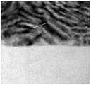
图1为本发明实施例1中制备修复层的截面图。FIG. 1 is a cross-sectional view of a repair layer prepared in Example 1 of the present invention.
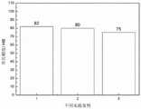
图2为本发明不同实施例中制备修复层的布氏硬度测量值。Figure 2 shows the Brinell hardness measurements of the prepared repair layers in different embodiments of the present invention.
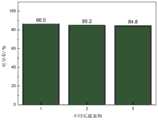
图3为本发明不同实施例中制备修复层的电导率测量值。Figure 3 is a measurement of the electrical conductivity of the prepared repair layer in various embodiments of the present invention.
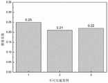
图4为本发明不同实施例中制备修复层的摩擦系数测量值。Figure 4 is a measurement of the coefficient of friction of the prepared repair layers in different embodiments of the present invention.
附图标记:修复层A、触头基材B。Reference numerals: repair layer A, contact base material B.
具体实施方式Detailed ways
以下结合具体实施例对本发明作进一步描述,但不限制本发明的保护范围和应用范围。The present invention is further described below in conjunction with specific embodiments, but does not limit the protection scope and application scope of the present invention.
实施例1Example 1
一种在磨损高压开关触头表面制备修复层的方法,包括以下步骤:A method for preparing a repair layer on the surface of a worn high-voltage switch contact, comprising the following steps:
1.试样预处理;先对35kV开关触头的磨损处用砂纸打磨至1200#,在丙酮溶液中超声波清洗10min,然后用蒸馏水冲洗干净,吹风机冷风吹干;1. Pre-treatment of the sample; first grind the worn parts of the 35kV switch contacts to 1200# with sandpaper, ultrasonically clean them in acetone solution for 10 minutes, then rinse them with distilled water, and dry them with a blower with cold air;
2.对预处理的试样进行激光重熔处理;激光重熔的工艺参数为:激光功率P为80W,扫描速度V为50mm/min,光斑直径D为2mm,搭接率M为15%,焦距H为209mm,保护气流L为2L/min;2. Carry out laser remelting treatment on the pretreated sample; the process parameters of laser remelting are: laser power P is 80W, scanning speed V is 50mm/min, spot diameter D is 2mm, overlap ratio M is 15%, The focal length H is 209mm, and the protective airflow L is 2L/min;
3.选取铜基合金粉末、钨基合金粉末、镍基合金粉、氧化石墨烯为熔覆材料,合金粉末的粒度为200~300目;对合金粉末进行干燥处理,干燥温度为120℃,时间为8h。3. Select copper-based alloy powder, tungsten-based alloy powder, nickel-based alloy powder, and graphene oxide as the cladding materials, and the particle size of the alloy powder is 200-300 mesh; the alloy powder is dried, and the drying temperature is 120 ° C and the time is 8h.
4.利用固体激光器对激光重熔处理后的试样进行激光熔覆处理,工艺参数为:激光功率P为800W,扫描速度V为180mm/min,光斑直径D为2mm,搭接率M为30%,送粉电压U为7V,焦距H为209mm,保护气流L为6L/min。4. Use a solid-state laser to carry out laser cladding treatment on the sample after laser remelting treatment. The process parameters are: laser power P is 800W, scanning speed V is 180mm/min, spot diameter D is 2mm, and overlap ratio M is 30 %, the powder feeding voltage U is 7V, the focal length H is 209mm, and the protective airflow L is 6L/min.
5.对激光熔覆处理后的试样进行后续处理,包括机加工、除油和打磨,使试样表面光洁,完成在铸铁表面制备无缺陷修复层。5. Follow-up processing of the samples after laser cladding treatment, including machining, degreasing and grinding, makes the surface of the samples smooth and completes the preparation of a defect-free repair layer on the surface of the cast iron.
如图1所示,采用扫描电镜对实施案例1所制备的样品截面进行分析,发现修复层A与触头基材B结合良好,修复层致密无空隙。As shown in Figure 1, the cross section of the sample prepared in Example 1 was analyzed by scanning electron microscope, and it was found that the repair layer A and the contact substrate B were well combined, and the repair layer was dense and free of voids.
如图2至图4所示,采用布氏硬度计测得修复层的硬度为:82HB,采用电导率检测仪测得电导率:86.5%,采用摩擦系数测试仪测得摩擦系数:0.25。As shown in Figures 2 to 4, the hardness of the repair layer measured by a Brinell hardness tester is: 82HB, the conductivity measured by a conductivity tester: 86.5%, and the friction coefficient measured by a friction coefficient tester: 0.25.
实施例2Example 2
一种在磨损高压开关触头表面制备修复层的方法,包括以下步骤:A method for preparing a repair layer on the surface of a worn high-voltage switch contact, comprising the following steps:
1.试样预处理;先对35kV开关触头的磨损处用砂纸打磨至1200#,在丙酮溶液中超声波清洗10min,然后用蒸馏水冲洗干净,吹风机冷风吹干;1. Pre-treatment of the sample; first grind the worn parts of the 35kV switch contacts to 1200# with sandpaper, ultrasonically clean them in acetone solution for 10 minutes, then rinse them with distilled water, and dry them with a blower with cold air;
2.选取铜基合金粉末、钨基合金粉末、铝合金粉末、氧化钪粉末为修复材料,合金粉末的粒度为200~300目;对铁基合金粉末进行干燥处理,干燥温度为100℃,时间为10h,干燥后送入光纤激光器的送粉装置。2. Select copper-based alloy powder, tungsten-based alloy powder, aluminum alloy powder, and scandium oxide powder as repair materials, and the particle size of the alloy powder is 200-300 mesh; the iron-based alloy powder is dried, and the drying temperature is 100 °C, and the time For 10h, after drying, it is sent to the powder feeding device of the fiber laser.
3.利用光纤激光器对激光重熔处理后的试样进行激光熔覆处理,工艺参数为:激光功率P为1800W,扫描速度V为540mm/min,光斑直径D为3mm,搭接率40%,送粉电压U为20V,焦距H为200mm,保护气流L为15L/min。3. Laser cladding is performed on the sample after laser remelting treatment with a fiber laser. The process parameters are: the laser power P is 1800W, the scanning speed V is 540mm/min, the spot diameter D is 3mm, and the lap rate is 40%. The powder feeding voltage U is 20V, the focal length H is 200mm, and the protective airflow L is 15L/min.
4.对激光熔覆处理后的试样进行后续处理,包括机加工、除油和打磨,使试样表面光洁,完成在铸铁表面制备无缺陷修复层。4. Follow-up processing of the samples after laser cladding treatment, including machining, degreasing and grinding, makes the surface of the samples smooth and completes the preparation of a defect-free repair layer on the surface of cast iron.
如图2至图4所示,采用布氏硬度计测得修复层的硬度为:80HB,采用电导率检测仪测得电导率:85.2%,采用摩擦系数测试仪测得摩擦系数:0.21。As shown in Figures 2 to 4, the hardness of the repair layer measured by a Brinell hardness tester is: 80HB, the conductivity measured by a conductivity tester: 85.2%, and the friction coefficient measured by a friction coefficient tester: 0.21.
实施例3Example 3
一种在磨损高压开关触头表面制备修复层的方法,包括以下步骤:A method for preparing a repair layer on the surface of a worn high-voltage switch contact, comprising the following steps:
1.试样预处理;先对35kV开关触头的磨损处用砂纸打磨至1200#,在丙酮溶液中超声波清洗10min,然后用蒸馏水冲洗干净,吹风机冷风吹干;1. Pre-treatment of the sample; first grind the worn parts of the 35kV switch contacts to 1200# with sandpaper, ultrasonically clean them in acetone solution for 10 minutes, then rinse them with distilled water, and dry them with a blower with cold air;
2.选取钴基合金粉末、镍基合金粉末、氧化铈粉末、石墨烯粉末为熔覆材料,合金粉末的粒度为200~300目;对钴基合金粉末进行干燥处理,干燥温度为120℃,时间为8h,干燥后送入光纤激光器的送粉装置。2. Select cobalt-based alloy powder, nickel-based alloy powder, cerium oxide powder, and graphene powder as cladding materials, and the particle size of the alloy powder is 200-300 mesh; the cobalt-based alloy powder is dried, and the drying temperature is 120 ℃, The time is 8h, and after drying, it is sent to the powder feeding device of the fiber laser.
5.利用光纤激光器对激光重熔处理后的试样进行激光熔覆处理,工艺参数为:激光功率P为2000W,扫描速度V为360mm/min,光斑直径D为3mm,搭接率50%,送粉电压U为30V,焦距H为200mm,保护气流L为15L/min。5. Use a fiber laser to perform laser cladding treatment on the sample after laser remelting treatment. The process parameters are: laser power P is 2000W, scanning speed V is 360mm/min, spot diameter D is 3mm, lap rate is 50%, The powder feeding voltage U is 30V, the focal length H is 200mm, and the protective airflow L is 15L/min.
6.对激光熔覆处理后的试样进行后续处理,包括机加工、除油和打磨,使试样表面光洁,完成在铸铁表面制备无缺陷修复层。6. Follow-up processing of the samples after laser cladding treatment, including machining, degreasing and grinding, makes the surface of the samples smooth and completes the preparation of a defect-free repair layer on the surface of cast iron.
如图2至图4所示,采用布氏硬度计测得修复层的硬度为75HB,采用电导率检测仪测得电导率:84.8%,采用摩擦系数测试仪测得摩擦系数:0.22。As shown in Figures 2 to 4, the hardness of the repair layer was measured by a Brinell hardness tester to be 75HB, the conductivity was measured by a conductivity tester: 84.8%, and the friction coefficient was measured by a friction coefficient tester: 0.22.
以上所述,仅为本发明的具体实施方式,但本发明的保护范围并不局限于此,任何不经过创造性劳动想到的变化或简单替换,都应该涵盖在本发明的保护范围之内。The above are only specific embodiments of the present invention, but the protection scope of the present invention is not limited thereto, and any changes or simple replacements that are not conceived of without creative work should be included within the protection scope of the present invention.
Claims (6)
Priority Applications (1)
| Application Number | Priority Date | Filing Date | Title |
|---|---|---|---|
| CN202010372003.3ACN111519184A (en) | 2020-05-06 | 2020-05-06 | Method for preparing repairing layer on surface of worn high-voltage switch contact |
Applications Claiming Priority (1)
| Application Number | Priority Date | Filing Date | Title |
|---|---|---|---|
| CN202010372003.3ACN111519184A (en) | 2020-05-06 | 2020-05-06 | Method for preparing repairing layer on surface of worn high-voltage switch contact |
Publications (1)
| Publication Number | Publication Date |
|---|---|
| CN111519184Atrue CN111519184A (en) | 2020-08-11 |
Family
ID=71908545
Family Applications (1)
| Application Number | Title | Priority Date | Filing Date |
|---|---|---|---|
| CN202010372003.3APendingCN111519184A (en) | 2020-05-06 | 2020-05-06 | Method for preparing repairing layer on surface of worn high-voltage switch contact |
Country Status (1)
| Country | Link |
|---|---|
| CN (1) | CN111519184A (en) |
Cited By (3)
| Publication number | Priority date | Publication date | Assignee | Title |
|---|---|---|---|---|
| CN113604718A (en)* | 2021-08-09 | 2021-11-05 | 内蒙古电力(集团)有限责任公司内蒙古电力科学研究院分公司 | Copper-based alloy powder material, preparation method and application thereof, cladding layer and preparation method thereof |
| CN114481118A (en)* | 2021-12-16 | 2022-05-13 | 中车工业研究院有限公司 | Method for repairing aluminum alloy by laser cladding in atmospheric environment |
| CN119549745A (en)* | 2024-12-09 | 2025-03-04 | 江西国创院新材料有限公司 | A preparation method of laser additive manufacturing copper alloy-tungsten copper composite electrical contact |
Citations (8)
| Publication number | Priority date | Publication date | Assignee | Title |
|---|---|---|---|---|
| CN101635210A (en)* | 2009-08-24 | 2010-01-27 | 西安理工大学 | Method for repairing defect in tungsten copper-copper integral electric contact material |
| CN101834077A (en)* | 2010-04-16 | 2010-09-15 | 河南理工大学 | A method of manufacturing pure copper/copper-chromium alloy composite contact material |
| CN105118702A (en)* | 2015-07-17 | 2015-12-02 | 河南科技大学 | Powder composition for copper alloy material, composite material layer, electric contact and preparation method of electric contact |
| CN106011841A (en)* | 2016-06-14 | 2016-10-12 | 重庆理工大学 | Preparation method of super-hard coating on surface of copper-chromium alloy |
| DE102015216754A1 (en)* | 2015-09-02 | 2017-03-02 | Siemens Aktiengesellschaft | Contact element for electrical switch and manufacturing process |
| CN107043933A (en)* | 2017-04-14 | 2017-08-15 | 广西大学 | A kind of method for preparing zero defect cladding layer in Cast Iron Surface |
| CN109267064A (en)* | 2018-11-09 | 2019-01-25 | 成都青石激光科技有限公司 | A kind of preparation method of ferrous alloy bearing shell wearing layer |
| CN110747458A (en)* | 2019-09-17 | 2020-02-04 | 上海宝钢工业技术服务有限公司 | Method for repairing crankshaft of hot-rolling fixed-width press |
- 2020
- 2020-05-06CNCN202010372003.3Apatent/CN111519184A/enactivePending
Patent Citations (8)
| Publication number | Priority date | Publication date | Assignee | Title |
|---|---|---|---|---|
| CN101635210A (en)* | 2009-08-24 | 2010-01-27 | 西安理工大学 | Method for repairing defect in tungsten copper-copper integral electric contact material |
| CN101834077A (en)* | 2010-04-16 | 2010-09-15 | 河南理工大学 | A method of manufacturing pure copper/copper-chromium alloy composite contact material |
| CN105118702A (en)* | 2015-07-17 | 2015-12-02 | 河南科技大学 | Powder composition for copper alloy material, composite material layer, electric contact and preparation method of electric contact |
| DE102015216754A1 (en)* | 2015-09-02 | 2017-03-02 | Siemens Aktiengesellschaft | Contact element for electrical switch and manufacturing process |
| CN106011841A (en)* | 2016-06-14 | 2016-10-12 | 重庆理工大学 | Preparation method of super-hard coating on surface of copper-chromium alloy |
| CN107043933A (en)* | 2017-04-14 | 2017-08-15 | 广西大学 | A kind of method for preparing zero defect cladding layer in Cast Iron Surface |
| CN109267064A (en)* | 2018-11-09 | 2019-01-25 | 成都青石激光科技有限公司 | A kind of preparation method of ferrous alloy bearing shell wearing layer |
| CN110747458A (en)* | 2019-09-17 | 2020-02-04 | 上海宝钢工业技术服务有限公司 | Method for repairing crankshaft of hot-rolling fixed-width press |
Non-Patent Citations (3)
| Title |
|---|
| 唐仕光等: "激光重熔处理对铝合金微弧氧化膜组织", 《材料工程》* |
| 左攀峰: "《学生毕业论文写作教程》", 31 August 2016, 北京:航空工业出版社* |
| 黎樵燊等: "《表面工程》", 30 November 2001, 北京:中国科学技术出版社* |
Cited By (6)
| Publication number | Priority date | Publication date | Assignee | Title |
|---|---|---|---|---|
| CN113604718A (en)* | 2021-08-09 | 2021-11-05 | 内蒙古电力(集团)有限责任公司内蒙古电力科学研究院分公司 | Copper-based alloy powder material, preparation method and application thereof, cladding layer and preparation method thereof |
| CN113604718B (en)* | 2021-08-09 | 2022-04-15 | 内蒙古电力(集团)有限责任公司内蒙古电力科学研究院分公司 | A copper-based alloy powder material, preparation method and application thereof, cladding layer and preparation method thereof |
| CN114481118A (en)* | 2021-12-16 | 2022-05-13 | 中车工业研究院有限公司 | Method for repairing aluminum alloy by laser cladding in atmospheric environment |
| CN114481118B (en)* | 2021-12-16 | 2023-11-10 | 中车工业研究院有限公司 | Method for repairing aluminum alloy by laser cladding in atmospheric environment |
| CN119549745A (en)* | 2024-12-09 | 2025-03-04 | 江西国创院新材料有限公司 | A preparation method of laser additive manufacturing copper alloy-tungsten copper composite electrical contact |
| CN119549745B (en)* | 2024-12-09 | 2025-08-05 | 江西国创院新材料有限公司 | A preparation method for laser additive manufacturing of copper alloy-tungsten copper composite electrical contacts |
Similar Documents
| Publication | Publication Date | Title |
|---|---|---|
| CN111519184A (en) | Method for preparing repairing layer on surface of worn high-voltage switch contact | |
| CN108611636A (en) | A kind of preparation method of wear resistant corrosion resistant composite coating | |
| CN101635210A (en) | Method for repairing defect in tungsten copper-copper integral electric contact material | |
| CN102528376B (en) | Electric spark precision repairing method for plastic mould | |
| CN103451650A (en) | Laser quick repair process method for large rotary machine bearing bush | |
| CN106011841A (en) | Preparation method of super-hard coating on surface of copper-chromium alloy | |
| CN104141129A (en) | Repairing method for threaded rod | |
| CN107043933A (en) | A kind of method for preparing zero defect cladding layer in Cast Iron Surface | |
| CN111455375A (en) | Method for repairing SiC coating of carbon/carbon composite material | |
| CN115505918B (en) | Repairing method for fatigue crack of aviation structural part | |
| CN111074266A (en) | Rapid forming and repairing method for damage of airplane electromagnetic pure iron part accessory | |
| CN102500912B (en) | Method for performing surface modification on metal by ultrasonic nano-welding | |
| CN113369728B (en) | Method for manufacturing titanium alloy large-scale complex structure component | |
| CN106757011A (en) | A kind of laser melting coating reproducing method of worm screw | |
| CN106435567A (en) | Laser cladding restoration method for compressor bearing shell | |
| CN106498386A (en) | A kind of laser melting coating copper surface composite coating and preparation method thereof | |
| CN112663040A (en) | Surface repairing method for isolating switch | |
| CN108213713A (en) | A kind of thin-wall part combined-repair method for increasing material based on pulse laser and continuous laser | |
| CN114643462B (en) | A kind of titanium alloy/stainless steel composite plate and preparation method thereof | |
| CN119549745B (en) | A preparation method for laser additive manufacturing of copper alloy-tungsten copper composite electrical contacts | |
| CN101618471B (en) | Metal surface vitrification method | |
| CN118492594A (en) | Method for prolonging service life of end face of aluminum alloy resistance spot welding electrode | |
| CN113604718A (en) | Copper-based alloy powder material, preparation method and application thereof, cladding layer and preparation method thereof | |
| CN107937860A (en) | A kind of preparation method of argon arc remelting Fe base wearing layers | |
| CN115369397A (en) | Corrosion fault repair method, composite coating and application of aerospace aluminum alloy parts |
Legal Events
| Date | Code | Title | Description |
|---|---|---|---|
| PB01 | Publication | ||
| PB01 | Publication | ||
| SE01 | Entry into force of request for substantive examination | ||
| SE01 | Entry into force of request for substantive examination | ||
| RJ01 | Rejection of invention patent application after publication | Application publication date:20200811 | |
| RJ01 | Rejection of invention patent application after publication |