CN111512710B - Substrates for printed wiring boards and printed wiring boards - Google Patents
Substrates for printed wiring boards and printed wiring boardsDownload PDFInfo
- Publication number
- CN111512710B CN111512710BCN201880083383.XACN201880083383ACN111512710BCN 111512710 BCN111512710 BCN 111512710BCN 201880083383 ACN201880083383 ACN 201880083383ACN 111512710 BCN111512710 BCN 111512710B
- Authority
- CN
- China
- Prior art keywords
- metal layer
- printed wiring
- base film
- wiring board
- copper
- Prior art date
- Legal status (The legal status is an assumption and is not a legal conclusion. Google has not performed a legal analysis and makes no representation as to the accuracy of the status listed.)
- Active
Links
Images


Classifications
- H—ELECTRICITY
- H05—ELECTRIC TECHNIQUES NOT OTHERWISE PROVIDED FOR
- H05K—PRINTED CIRCUITS; CASINGS OR CONSTRUCTIONAL DETAILS OF ELECTRIC APPARATUS; MANUFACTURE OF ASSEMBLAGES OF ELECTRICAL COMPONENTS
- H05K1/00—Printed circuits
- H05K1/02—Details
- H05K1/09—Use of materials for the conductive, e.g. metallic pattern
- H05K1/092—Dispersed materials, e.g. conductive pastes or inks
- H—ELECTRICITY
- H05—ELECTRIC TECHNIQUES NOT OTHERWISE PROVIDED FOR
- H05K—PRINTED CIRCUITS; CASINGS OR CONSTRUCTIONAL DETAILS OF ELECTRIC APPARATUS; MANUFACTURE OF ASSEMBLAGES OF ELECTRICAL COMPONENTS
- H05K3/00—Apparatus or processes for manufacturing printed circuits
- H05K3/38—Improvement of the adhesion between the insulating substrate and the metal
- B—PERFORMING OPERATIONS; TRANSPORTING
- B32—LAYERED PRODUCTS
- B32B—LAYERED PRODUCTS, i.e. PRODUCTS BUILT-UP OF STRATA OF FLAT OR NON-FLAT, e.g. CELLULAR OR HONEYCOMB, FORM
- B32B15/00—Layered products comprising a layer of metal
- B32B15/04—Layered products comprising a layer of metal comprising metal as the main or only constituent of a layer, which is next to another layer of the same or of a different material
- H—ELECTRICITY
- H05—ELECTRIC TECHNIQUES NOT OTHERWISE PROVIDED FOR
- H05K—PRINTED CIRCUITS; CASINGS OR CONSTRUCTIONAL DETAILS OF ELECTRIC APPARATUS; MANUFACTURE OF ASSEMBLAGES OF ELECTRICAL COMPONENTS
- H05K2201/00—Indexing scheme relating to printed circuits covered by H05K1/00
- H05K2201/01—Dielectrics
- H05K2201/0137—Materials
- H05K2201/0154—Polyimide
- H—ELECTRICITY
- H05—ELECTRIC TECHNIQUES NOT OTHERWISE PROVIDED FOR
- H05K—PRINTED CIRCUITS; CASINGS OR CONSTRUCTIONAL DETAILS OF ELECTRIC APPARATUS; MANUFACTURE OF ASSEMBLAGES OF ELECTRICAL COMPONENTS
- H05K2201/00—Indexing scheme relating to printed circuits covered by H05K1/00
- H05K2201/03—Conductive materials
- H05K2201/0332—Structure of the conductor
- H05K2201/0335—Layered conductors or foils
- H05K2201/0338—Layered conductor, e.g. layered metal substrate, layered finish layer or layered thin film adhesion layer
- H—ELECTRICITY
- H05—ELECTRIC TECHNIQUES NOT OTHERWISE PROVIDED FOR
- H05K—PRINTED CIRCUITS; CASINGS OR CONSTRUCTIONAL DETAILS OF ELECTRIC APPARATUS; MANUFACTURE OF ASSEMBLAGES OF ELECTRICAL COMPONENTS
- H05K2201/00—Indexing scheme relating to printed circuits covered by H05K1/00
- H05K2201/03—Conductive materials
- H05K2201/0332—Structure of the conductor
- H05K2201/0335—Layered conductors or foils
- H05K2201/0361—Etched tri-metal structure, i.e. metal layers or metal patterns on both sides of a different central metal layer which is later at least partly etched
- H—ELECTRICITY
- H05—ELECTRIC TECHNIQUES NOT OTHERWISE PROVIDED FOR
- H05K—PRINTED CIRCUITS; CASINGS OR CONSTRUCTIONAL DETAILS OF ELECTRIC APPARATUS; MANUFACTURE OF ASSEMBLAGES OF ELECTRICAL COMPONENTS
- H05K2203/00—Indexing scheme relating to apparatus or processes for manufacturing printed circuits covered by H05K3/00
- H05K2203/11—Treatments characterised by their effect, e.g. heating, cooling, roughening
- H05K2203/1131—Sintering, i.e. fusing of metal particles to achieve or improve electrical conductivity
- H—ELECTRICITY
- H05—ELECTRIC TECHNIQUES NOT OTHERWISE PROVIDED FOR
- H05K—PRINTED CIRCUITS; CASINGS OR CONSTRUCTIONAL DETAILS OF ELECTRIC APPARATUS; MANUFACTURE OF ASSEMBLAGES OF ELECTRICAL COMPONENTS
- H05K3/00—Apparatus or processes for manufacturing printed circuits
- H05K3/02—Apparatus or processes for manufacturing printed circuits in which the conductive material is applied to the surface of the insulating support and is thereafter removed from such areas of the surface which are not intended for current conducting or shielding
- H05K3/06—Apparatus or processes for manufacturing printed circuits in which the conductive material is applied to the surface of the insulating support and is thereafter removed from such areas of the surface which are not intended for current conducting or shielding the conductive material being removed chemically or electrolytically, e.g. by photo-etch process
- H—ELECTRICITY
- H05—ELECTRIC TECHNIQUES NOT OTHERWISE PROVIDED FOR
- H05K—PRINTED CIRCUITS; CASINGS OR CONSTRUCTIONAL DETAILS OF ELECTRIC APPARATUS; MANUFACTURE OF ASSEMBLAGES OF ELECTRICAL COMPONENTS
- H05K3/00—Apparatus or processes for manufacturing printed circuits
- H05K3/38—Improvement of the adhesion between the insulating substrate and the metal
- H05K3/388—Improvement of the adhesion between the insulating substrate and the metal by the use of a metallic or inorganic thin film adhesion layer
Landscapes
- Engineering & Computer Science (AREA)
- Microelectronics & Electronic Packaging (AREA)
- Chemical & Material Sciences (AREA)
- Dispersion Chemistry (AREA)
- Manufacturing & Machinery (AREA)
- Manufacturing Of Printed Wiring (AREA)
- Parts Printed On Printed Circuit Boards (AREA)
- Laminated Bodies (AREA)
Abstract
Description
Translated fromChinese技术领域technical field
本公开涉及一种印刷线路板用基材和印刷线路板。The present disclosure relates to a base material for a printed wiring board and a printed wiring board.
本申请基于并要求于2017年12月25日提交的日本专利申请No.2017-247550的优先权,该日本专利申请的全部内容通过引用方式并入本文。This application is based on and claims priority from Japanese Patent Application No. 2017-247550 filed on December 25, 2017, the entire contents of which are incorporated herein by reference.
背景技术Background technique
已知这样一种印刷线路板用基材,其中金属箔经由粘合剂层从而层叠在绝缘性基膜的表面上。而且,为了应对近来电子部件尺寸的减小,还提出了其中金属层直接层叠在基膜的表面上的印刷线路板用基材。作为这样的印刷线路板用基材,提出了使用溅射法将晶种层层叠在基膜的表面上的印刷线路板用基材(参见日本待审查专利公开No.2011-37214)。There is known a base material for a printed wiring board in which a metal foil is laminated on the surface of an insulating base film via an adhesive layer. Also, in order to cope with the recent reduction in size of electronic components, substrates for printed wiring boards in which a metal layer is directly laminated on the surface of a base film have also been proposed. As such a substrate for a printed wiring board, a substrate for a printed wiring board in which a seed layer is laminated on the surface of a base film using a sputtering method has been proposed (see Japanese Unexamined Patent Publication No. 2011-37214).
在上述出版物中描述的印刷线路板用基材包括由聚酰亚胺膜制成的基膜和层叠在该基膜的表面上的晶种层(底层)。晶种层是通过利用溅射法在基膜的表面上依次层叠镍-铬合金层和铜层而形成的。The base material for a printed wiring board described in the above publication includes a base film made of a polyimide film and a seed layer (underlayer) laminated on the surface of the base film. The seed layer is formed by sequentially laminating a nickel-chromium alloy layer and a copper layer on the surface of the base film by sputtering.
[现有技术文献][Prior art literature]
[专利文件][Patent Document]
[专利文献1]日本待审查专利公开No.2011-37214[Patent Document 1] Japanese Unexamined Patent Publication No. 2011-37214
发明内容Contents of the invention
根据本公开的一个方面,一种印刷线路板用基材包括:绝缘性基膜;以及金属层,该金属层层叠在基膜的至少一个表面上并且包含铜作为主要成分,其中,在金属层中距金属层与基膜的界面100nm以下的区域中,每单位面积的含量为:Cr<0.1mg/m2,并且Ni<0.1mg/m2,并且其中基膜的层叠有金属层的表面的算术平均粗糙度(Sa)小于0.10μm。According to an aspect of the present disclosure, a base material for a printed wiring board includes: an insulating base film; and a metal layer laminated on at least one surface of the base film and containing copper as a main component, wherein the metal layer In the region below 100nm from the interface between the metal layer and the base film, the content per unit area is: Cr<0.1mg/m2 , and Ni<0.1mg/m2 , and the surface of the base film where the metal layer is laminated The arithmetic average roughness (Sa) is less than 0.10μm.
根据本公开的另一方面,一种印刷线路板使用印刷线路板用基材。According to another aspect of the present disclosure, a printed wiring board uses a base material for a printed wiring board.
附图说明Description of drawings
图1为示出了根据本公开的一个实施方案的印刷线路板用基材的示意性截面图;1 is a schematic cross-sectional view showing a substrate for a printed wiring board according to an embodiment of the present disclosure;
图2为示出了根据与图1的印刷线路板用基材不同的实施方案的印刷线路板用基材的示意性截面图;2 is a schematic sectional view showing a substrate for a printed wiring board according to an embodiment different from that of FIG. 1;
图3为示出了使用图2的印刷线路板用基材的印刷线路板的示意性截面图;3 is a schematic sectional view showing a printed wiring board using the base material for a printed wiring board of FIG. 2;
图4A为示出了图1的印刷线路板用基材的制造方法的涂层形成步骤的示意性截面图;4A is a schematic cross-sectional view showing a coating layer forming step of the method of manufacturing the base material for a printed wiring board of FIG. 1;
图4B为示出了图1的印刷线路板用基材的制造方法的金属层形成步骤的示意性截面图;4B is a schematic cross-sectional view showing a metal layer forming step of the method of manufacturing the base material for a printed wiring board of FIG. 1;
图4C为示出了图2的印刷线路板用基材的制造方法的电镀层层叠步骤的示意性截面图;和4C is a schematic cross-sectional view showing a plating layer lamination step of the manufacturing method of the base material for a printed wiring board of FIG. 2; and
图5为示出了图3的印刷线路板的制造方法的蚀刻步骤的示意性截面图。5 is a schematic cross-sectional view illustrating an etching step of the method of manufacturing the printed wiring board of FIG. 3 .
具体实施方式Detailed ways
[本公开待解决的问题][Issues to be resolved in this disclosure]
如上述出版物中所述,在使用溅射方法形成晶种层的情况下,在基膜与铜层之间设置镍铬合金层以增强耐迁移性。然而,镍和铬比铜更难蚀刻。另外,在基膜与铜层之间存在镍铬合金层的情况下,需要分别进行铜层的蚀刻和镍铬合金层的蚀刻。因此,上述出版物中描述的印刷线路板用基材趋于需要长时间的蚀刻并且降低了蚀刻精度。因此,根据该印刷线路板用基材,难以形成精细线路。As described in the aforementioned publication, in the case of forming the seed layer using the sputtering method, a nichrome layer is provided between the base film and the copper layer to enhance migration resistance. However, nickel and chromium are more difficult to etch than copper. In addition, when there is a nichrome layer between the base film and the copper layer, it is necessary to perform etching of the copper layer and etching of the nichrome layer separately. Therefore, the base material for a printed wiring board described in the above-mentioned publication tends to require a long time for etching and lowers the etching precision. Therefore, according to this base material for printed wiring boards, it is difficult to form a fine line.
鉴于上述,本公开的目的在于提供一种能够容易地形成精细线路的印刷线路板用基材和印刷线路板。In view of the above, an object of the present disclosure is to provide a substrate for a printed wiring board and a printed wiring board capable of easily forming fine lines.
[本公开的效果][Effect of this disclosure]
根据本公开的印刷线路板用基材和印刷线路板能够容易地形成精细线路。The base material for a printed wiring board and the printed wiring board according to the present disclosure can easily form fine wiring.
[本公开的实施方案的描述][Description of Embodiments of the Present Disclosure]
首先,将列出并描述本公开的各方面。First, various aspects of the present disclosure will be listed and described.
根据本公开的一个方面,一种印刷线路板用基材包括:绝缘性基膜;以及金属层,该金属层层叠在基膜的至少一个表面上并且包含铜作为主要成分,其中,在金属层中距金属层与基膜的界面100nm以下的区域中,每单位面积的含量为:Cr<0.1mg/m2,并且Ni<0.1mg/m2,并且其中基膜的层叠有金属层的表面的算术平均粗糙度(Sa)小于0.10μm。According to an aspect of the present disclosure, a base material for a printed wiring board includes: an insulating base film; and a metal layer laminated on at least one surface of the base film and containing copper as a main component, wherein the metal layer In the region below 100nm from the interface between the metal layer and the base film, the content per unit area is: Cr<0.1mg/m2 , and Ni<0.1mg/m2 , and the surface of the base film where the metal layer is laminated The arithmetic average roughness (Sa) is less than 0.10μm.
在印刷线路板用基材中,由于金属层中距金属层与基膜的界面100nm以下的区域中的每单位面积的Cr和Ni的含量小并且在上述范围内,因此金属层的蚀刻比较容易。另外,在印刷线路板用基材中,由于基膜的层叠有金属层的表面的算术平均粗糙度(Sa)在上述范围内,因此可以抑制由于基膜表面上的凸起/凹陷而导致的蚀刻精度的降低。因此,根据印刷线路板用基材,可以高精度地进行蚀刻。因此,印刷线路板用基材能够容易地形成精细线路。In the base material for printed wiring boards, since the content of Cr and Ni per unit area in the region of the metal layer below 100 nm from the interface between the metal layer and the base film is small and within the above range, the etching of the metal layer is relatively easy . In addition, in the substrate for printed wiring boards, since the arithmetic mean roughness (Sa) of the surface of the base film on which the metal layer is laminated is within the above-mentioned range, it is possible to suppress roughness due to protrusions/depressions on the surface of the base film. Decrease in etching precision. Therefore, according to the base material for printed wiring boards, etching can be performed with high precision. Therefore, the substrate for a printed wiring board can easily form a fine circuit.
金属层优选包含固定在基膜上的铜颗粒的烧结体。以这种方式,通过使金属层包含固定在基膜上的铜颗粒的烧结体,可以以低成本形成精细线路,而无需诸如溅射之类的物理气相沉积所需的昂贵的真空设备。The metal layer preferably comprises a sintered body of copper particles fixed on the base film. In this way, by making the metal layer contain a sintered body of copper particles fixed on the base film, fine wiring can be formed at low cost without expensive vacuum equipment required for physical vapor deposition such as sputtering.
烧结体的平均粒径优选为50nm以上300nm以下。通过使烧结体的平均粒径在上述范围内,可以容易且可靠地形成致密的金属层,因此容易形成精细电路。The average particle diameter of the sintered body is preferably not less than 50 nm and not more than 300 nm. When the average particle size of the sintered body is within the above range, a dense metal layer can be easily and reliably formed, and thus a fine circuit can be easily formed.
优选地,在金属层中距金属层与基膜的界面100nm以下的区域中,每单位面积的含量为:Pd<0.1mg/m2。在上述区域中的Pd的含量高的情况下,除了用于去除铜的蚀刻之外,还需要用于去除Pd的蚀刻。相对于此,通过使金属层中距金属层与基膜的界面100nm以下的区域中的每单位面积的Pd的含量在上述范围内,则无需另外进行蚀刻去除Pd即可形成精细线路。Preferably, the content per unit area of the metal layer is: Pd<0.1 mg/m2 in a region within 100 nm from the interface between the metal layer and the base film. When the content of Pd in the above region is high, etching for removing Pd is required in addition to etching for removing copper. On the other hand, by setting the Pd content per unit area in the metal layer within 100 nm from the interface between the metal layer and the base film within the above range, fine lines can be formed without additional etching to remove Pd.
优选地,在金属层中距金属层与基膜的界面100nm以下的区域中,每单位面积的含量为:0.001mg/m2≤Ti≤0.05mg/m2。通过使金属层中距金属层与基膜的界面100nm以下的区域中的每单位面积的Ti的含量在上述范围内,可以抑制铜向基膜的扩散,从而可以形成致密的金属层。Preferably, the content per unit area in the metal layer within 100 nm from the interface between the metal layer and the base film is: 0.001 mg/m2 ≤ Ti ≤ 0.05 mg/m2 . By setting the Ti content per unit area in the metal layer within 100 nm from the interface between the metal layer and the base film within the above range, diffusion of copper into the base film can be suppressed and a dense metal layer can be formed.
烧结体的平均粒径优选为70nm以上200nm以下。根据该构成,可以形成精细线路。The average particle diameter of the sintered body is preferably not less than 70 nm and not more than 200 nm. According to this configuration, fine lines can be formed.
根据本公开的另一方面,一种印刷线路板使用该印刷线路板用基材。因为印刷线路板使用该印刷线路板用基材,所以易于形成精细线路。According to another aspect of the present disclosure, a printed wiring board uses the base material for a printed wiring board. Since the base material for a printed wiring board is used for a printed wiring board, it is easy to form a fine circuit.
优选的是,印刷线路板包括位于金属层的外表面上的电镀层。因为印刷线路板的金属层致密,所以可以在金属层的外表面上直接设置电镀层,而无需在金属层的外表面上层叠化学镀层。其结果是,可以提高制造效率并且可以促进成本降低。Preferably, the printed wiring board includes a plating layer on the outer surface of the metal layer. Because the metal layer of the printed wiring board is dense, an electroplating layer can be directly provided on the outer surface of the metal layer without stacking an electroless plating layer on the outer surface of the metal layer. As a result, manufacturing efficiency can be improved and cost reduction can be promoted.
需要说明的是,在本公开中,“主要成分”是指质量含量最大的成分,例如是指含量为50质量%以上的成分,优选含量为80质量%以上的成分,并且更优选含量为90质量%以上的成分。“金属层中距金属层与基膜的界面100nm以下的区域中的每单位面积的含量”是指通过ICP-MS(电感耦合等离子体质谱法)测定的值。“算术平均粗糙度(Sa)”是指通过对JIS-B0601:2001中定义的“算术平均粗糙度(Ra)”进行三维扩展而得到的参数,并且是在30μm×30μm的测量范围内且截断值为90时测量的值。“烧结体的平均粒径”是指通过表面SEM测定的粒径分布中的体积累积值为50%时的粒径。It should be noted that, in the present disclosure, "main component" refers to the component with the largest mass content, for example, it refers to a component with a content of 50% by mass or more, preferably a component with a content of 80% by mass or more, and more preferably a content of 90% by mass. Components above mass %. "Content per unit area in the region of 100 nm or less from the interface of a metal layer and a base film in a metal layer" means the value measured by ICP-MS (Inductively Coupled Plasma Mass Spectrometry). "Arithmetic mean roughness (Sa)" refers to the parameter obtained by three-dimensional extension of "arithmetic mean roughness (Ra)" defined in JIS-B0601:2001, and is within the measurement range of 30μm×30μm and truncated The value measured when the value is 90. The "average particle diameter of the sintered body" refers to the particle diameter when the cumulative volume value in the particle diameter distribution measured by surface SEM is 50%.
[本公开的实施方案的细节][Details of Embodiments of the Present Disclosure]
在下文中,将参考附图描述本公开的优选实施方案。Hereinafter, preferred embodiments of the present disclosure will be described with reference to the accompanying drawings.
[第一实施方案][First Embodiment]
<印刷线路板用基材><Substrates for printed wiring boards>
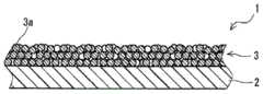
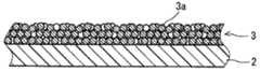
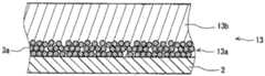
图1所示的印刷线路板用基材1包括绝缘性基膜2和金属层3,该金属层3层叠在基膜2的一个表面上并且包含铜作为主要成分。印刷线路板用基材1是柔性印刷线路板用基材,并且具有柔性。在印刷线路板用基材1中,金属层3中距金属层3与基膜2的界面100nm以下的区域中的每单位面积的含量为:Cr<0.1mg/m2,并且Ni<0.1mg/m2。此外,在印刷线路板用基材1中,基膜2的层叠有金属层3的表面的算术平均粗糙度(Sa)小于0.10μm。A substrate 1 for a printed wiring board shown in FIG. 1 includes an insulating
在印刷线路板用基材1中,因为金属层3中距金属层3与基膜2的界面100nm以下的区域中的每单位面积的Cr和Ni的含量小并且在上述范围内,因此,金属层3的蚀刻比较容易。例如,不需要分别进行铜的蚀刻以及Cr和Ni的蚀刻。另外,在印刷线路板用基材1中,由于基膜2的层叠有金属层3的表面的算术平均粗糙度(Sa)在上述范围内,因此可以抑制由于基膜2的表面上的突起/凹陷而导致的蚀刻精度的降低。因此,根据印刷线路板用基材1,可以以高精度进行蚀刻。因此,印刷线路板用基材1能够容易地形成精细线路。In the substrate 1 for a printed wiring board, since the content of Cr and Ni per unit area in the region below 100 nm from the interface between the
(金属层3)(metal layer 3)
金属层3构成印刷线路板用基材1的晶种层。金属层3直接层叠(即,不插入诸如粘合剂层之类的另一层)在基膜2的一个表面上。金属层3包含固定在基膜2上的铜颗粒的烧结体3a。即,金属层3不是通过溅射法形成的。因为印刷线路板用基材1不需要诸如溅射之类的物理气相沉积所需的昂贵的真空设备,所以当形成金属层3时,可以以低成本形成精细线路。另外,由于不是通过溅射法形成金属层3,因此即使金属层3中距金属层3与基膜2的界面100nm以下的区域中的Cr和Ni的含量降低,印刷线路板用基材1也具有足够的抗迁移性。The
在印刷线路板用基材1中,通过调节金属层3中距金属层3与基膜2的界面100nm以下的区域中每单位面积的金属成分的含量,可以容易地形成精细线路。在金属层3中距金属层3与基膜2的界面100nm以下的区域中,每单位面积的铜(Cu)的含量的下限优选为500mg/m2,更优选为600mg/m2。当上述区域中的每单位面积的Cu的含量小于该下限时,可能难以形成廉价的、具有低电阻且具有优异的蚀刻性能的金属层3。另一方面,上述区域中每单位面积的Cu的含量的上限例如可以为894mg/m2,以易于与其他成分的调整,这将在后面描述。In the base material 1 for a printed wiring board, fine wiring can be easily formed by adjusting the content of the metal component per unit area in the region of the
如上所述,金属层3中距金属层3与基膜2的界面100nm以下的区域中的每单位面积的Cr含量小于0.1mg/m2。因为Cr比铜更难于蚀刻,所以当上述区域中每单位面积的Cr含量超过该上限时,蚀刻精度劣化,因此难以形成包括精细线路的印刷线路板。此外,当上述区域中的每单位面积的Cr含量超过该上限时,可能需要分别进行铜的蚀刻以及Cr的蚀刻,从而导致更长的蚀刻时间并且降低了印刷线路板的制造效率。上述区域中的每单位面积的Cr含量的上限优选为0.05mg/m2,更优选为0.01mg/m2。通过使上述区域中的每单位面积的Cr含量小于上限,可以容易地进行蚀刻,并且可以提高蚀刻精度。另一方面,对于上述区域中每单位面积的Cr含量的下限没有特别限制,可以为0.00mg/m2。As described above, the Cr content per unit area in the region 100 nm or less from the interface between the
如上所述,金属层3中距金属层3与基膜2的界面100nm以下的区域中的每单位面积的Ni含量小于0.1mg/m2。因为Ni比铜更难于蚀刻,所以当上述区域中每单位面积的Ni含量超过该上限时,蚀刻精度劣化,因此难以形成包括精细线路的印刷线路板。此外,当上述区域中的每单位面积的Ni含量超过该上限时,可能需要分别进行铜的蚀刻以及Ni的蚀刻,从而导致更长的蚀刻时间并且降低了印刷线路板的制造效率。上述区域中的每单位面积的Ni含量的上限优选为0.05mg/m2,更优选为0.01mg/m2。通过使上述区域中的每单位面积的Ni含量小于上限,可以容易地进行蚀刻,并且可以进一步提高蚀刻精度。另一方面,对于上述区域中每单位面积的Ni含量的下限没有特别限制,可以为0.00mg/m2。As described above, the Ni content per unit area in the region within 100 nm from the interface between the
优选的是,金属层3中距金属层3与基膜2的界面100nm以下的区域中的每单位面积的钯(Pd)的含量小于0.1mg/m2。另外,上述区域中的每单位面积的Pd的含量的上限更优选为0.05mg/m2。通常,在基膜的一个表面上层叠金属层的情况下,使含Pd的催化剂附着在基膜的该表面上,然后通过化学镀铜形成金属层。然而,根据该构成,上述区域中的Pd含量增加,并且除了用于去除铜的蚀刻之外,还需要进行蚀刻以去除Pd。相对于此,在印刷线路板用基材1中,由于可以不进行化学镀覆而形成致密的金属层3,因此易于将Pd的含量调整至上述范围内。通过使上述区域中的每单位面积的Pd含量在上述范围内,可以形成精细线路而无需进行用以去除Pd的蚀刻。应注意,对于上述区域中的每单位面积的Pd含量的下限没有特别限制,并且可以为0.00mg/m2。Preferably, the palladium (Pd) content per unit area in the
金属层3中距金属层3与基膜2的界面100nm以下的区域中的每单位面积的Ti含量的下限优选为0.001mg/m2,更优选为0.01mg/m2。另一方面,上述区域中的每单位面积的Ti含量的上限优选为0.05mg/m2,更优选为0.04mg/m2。如下所述,例如使用通过钛氧化还原法得到的铜颗粒形成金属层3。因此,易于将上述区域中的每单位面积的Ti含量调整至上述范围内。通过使Ti以层状结构在金属层3中析出,可以抑制铜扩散到基膜2中。当上述区域中的每单位面积的Ti含量小于上述下限时,不能充分抑制铜扩散进入基膜2中。相反,当上述区域中的每单位面积的Ti含量超过上述上限时,蚀刻可能不容易进行并且可能无法充分提高蚀刻精度。The lower limit of the Ti content per unit area in the
金属层3中距金属层3与基膜2的界面100nm以下的区域中的每单位面积的钠(Na)含量的下限优选大于0mg/m2,更优选为1mg/m2。另一方面,上述区域中每单位面积的Na含量的上限优选为50mg/m2,更优选为40mg/m2。当上述区域中的每单位面积的Na含量小于上述下限时,则烧结体3a与基膜2的密着性可能不充分,或者铜可能会扩散到基膜2中。相反,当上述区域中的每单位面积的Na含量超过上述上限时,可能难以进行蚀刻,并且可能无法充分提高蚀刻精度。The lower limit of the sodium (Na) content per unit area in the
应当注意的是,可以通过(例如)使用具有适当浓度的氢氧化钠溶液对基膜2的层叠金属层3的表面进行碱处理,从而调节上述区域中每单位面积的Na含量。It should be noted that the Na content per unit area in the above region can be adjusted by, for example, subjecting the surface of
优选在基膜2与金属层3之间的界面附近存在氧化铜(CuO或Cu2O)或来源于氧化铜的基团。当烧结下述涂膜等时,基于导电性油墨中包含的铜颗粒而产生氧化铜或来源于氧化铜的基团。应注意,“基膜与金属层之间的界面附近”是指在厚度方向上距基膜与金属层的界面规定范围内的区域,优选为在厚度方向上距该界面0.1nm以上20nm以下的区域。It is preferable that copper oxide (CuO or Cu2 O) or a group derived from copper oxide exist in the vicinity of the interface between
在基膜2与金属层3之间的界面附近,氧化铜或来源于氧化铜的基团的每单位面积的含量的下限优选为0.10μg/cm2,更优选为0.15μg/cm2。另一方面,该含量的上限优选为10μg/cm2,更优选为5μg/cm2。当含量低于上述下限时,烧结体3a与基膜2的密着性不充分,或者铜可能扩散到基膜2中。相反,当该含量超过上述上限时,可能难以控制导电性油墨的热处理。The lower limit of the content per unit area of copper oxide or groups derived from copper oxide near the interface between
烧结体3a的平均粒径的下限优选为50nm,更优选为70nm。另一方面,烧结体3a的平均粒径的上限优选为300nm,更优选为200nm。The lower limit of the average particle diameter of the
当烧结体3a的平均粒径小于上述下限时,金属层3的抗氧化性可能会降低。相反,当烧结体3a的平均粒径超过上述上限时,可能难以形成足够致密的金属层3。When the average particle diameter of the
金属层3的平均厚度的下限优选为100nm,更优选为200nm。另一方面,金属层3的平均厚度的上限优选为1000nm,更优选为500nm。通过将金属层3的平均厚度设定为上述下限值以上,可以降低金属层3的电阻,因此在应用于制造用于(例如)射频信号处理用印刷线路板时,可以抑制传输损失。另一方面,当金属层3的平均厚度超过上述上限时,金属层3可能不必要地变厚,并且印刷线路板用基材1的制造效率可能会降低。The lower limit of the average thickness of the
(基膜)(basement membrane)
基膜2是绝缘的。基膜2的主要成分的实例包括诸如聚酰亚胺、液晶聚酯、聚对苯二甲酸乙二醇酯、聚萘二甲酸乙二醇酯、含氟聚合物等软质材料。其中,由于聚酰亚胺、液晶聚酯、聚对苯二甲酸乙二醇酯以及它们的组合与烧结体3a的结合强度高,因而是优选的,聚酰亚胺是更优选的。应当注意,基膜2可以是多孔的,或者可以包含填料、添加剂等。The
对于基膜2的厚度没有特别的限制。例如,基膜2的平均厚度的下限优选为5μm,并且更优选为12μm。另一方面,基膜2的平均厚度的上限优选为2mm,更优选为1.6mm。当基膜2的平均厚度小于上述下限时,基膜2的强度可能不足。相反,当基膜2的平均厚度超过上述上限时,可能难以应用于需要减小厚度的电子设备,并且柔性可能不足。There is no particular limitation on the thickness of the
在使用后述的导电性油墨形成烧结体3a的情况下,优选对基膜2的层叠金属层3的表面(烧结体3a的固定面)进行亲水化处理。作为亲水化处理,例如,可以使用通过等离子体照射使固定面亲水化的等离子体处理或通过碱性溶液使固定面亲水化的碱处理。由于通过对固定面进行亲水化处理降低了导电性油墨相对于固定面的表面张力,因此可以将导电性油墨均匀地涂布于固定面上。When the
如上所述,基膜2的层叠有金属层3的表面的算术平均粗糙度(Sa)小于0.10μm。另外,算术平均粗糙度(Sa)的上限优选为0.05μm。当算术平均粗糙度(Sa)超过上限时,对基膜2的表面的凹部的蚀刻可能不容易,并且蚀刻精度可能会降低。另外,在射频传播到金属层3的情况下,由于趋肤效应,信号沿着基膜2的表面的凹凸传输,因此行进距离可能变长并且损耗可能会增大。另一方面,对于算术平均粗糙度(Sa)的下限没有特别限制,例如可以为0.00μm。As described above, the arithmetic mean roughness (Sa) of the surface of the
(基膜与金属层之间的剥离强度)(Peel strength between base film and metal layer)
基膜2与金属层3之间的剥离强度的下限优选为6N/cm,更优选为8N/cm。通过使剥离强度为上述下限值以上,可以防止基膜2与金属层3之间的剥离,并且可以形成电连接可靠性高的印刷线路板。另一方面,对于剥离强度的上限没有特别的限制,例如可以为20N/cm。剥离强度可以通过例如固定在基膜2上的烧结体3a的量、导电性油墨中的铜颗粒的尺寸、后述的涂膜在烧结时的烧结温度和烧结时间来控制。应当注意,“剥离强度”是指根据JIS-C6471:1995在180°方向剥离试验中获得的剥离强度。The lower limit of the peel strength between the
[第二实施方案][Second Embodiment]
<印刷线路板用基材><Substrates for printed wiring boards>
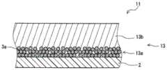
接下来,将参照图2描述根据本公开的第二实施方案的印刷线路板用基材11。印刷线路板用基材11包括:绝缘性基膜2;和金属层13,金属层13层叠在基膜2的一个表面上,并且包含铜作为主要成分。印刷线路板用基材11是柔性印刷线路板用基材,并且具有柔性。金属层13包括晶种层13a和层叠在晶种层13a的外表面上的电镀层13b,晶种层13a由直接层叠在基膜2上的图1的金属层3构成。印刷线路板用基材11具有与图1的印刷线路板用基材1相似的构成,不同之处在于,金属层13包括层叠在晶种层13a的外表面上的电镀层13b。因此,下面将仅描述电镀层13b。Next, a base material 11 for a printed wiring board according to a second embodiment of the present disclosure will be described with reference to FIG. 2 . The base material 11 for a printed wiring board includes: an insulating
(电镀层)(Plating)
电镀层13b直接层叠在晶种层13a的外表面上。电镀层13b包括通过电镀形成的电镀铜。电镀铜优选层叠在晶种层13a的外表面上,并且构成晶种层13a的烧结体3a之间的间隙填充有电镀铜。The
因为晶种层13a致密地形成于印刷线路板用基材11中,所以电镀层13b可直接层叠于晶种层13a的外表面上,而无需插入化学镀层。通过使印刷线路板用基材11包括电镀层13b,可以增加金属层13的厚度并且可以减小金属层13的电阻。因此,根据印刷线路板用基材11,例如,在用于制造用于射频信号处理的印刷线路板的情况下,可以抑制传输损耗。另外,根据印刷线路板用基材11,通过在晶种层13a的外表面上直接层叠电镀层13b,在减小金属层13的电阻的同时,可以容易地抑制异种金属混入金属层13中。由此,能够容易且可靠地将金属层13中距金属层13与基膜2的界面100nm以下的区域中的各种金属成分的含量调整至上述范围内。Since the
通过使金属层13包括电镀层13b,可以在相对短的时间内容易且可靠地调节厚度。根据待制造的印刷线路的构成来设定金属层13的平均厚度,对其没有特别限制,金属层13的厚度的下限优选为1μm,更优选为2μm。另一方面,平均厚度的上限优选为100μm,更优选为50μm。当平均厚度小于上述下限时,金属层13容易受损。相反,当平均厚度超过上述上限时,可能难以应用于需要减小厚度的电子设备。By making the
[第三实施方案][Third Embodiment]
<印刷线路板><Printed circuit board>
图3的印刷线路板21使用了图2的印刷线路板用基材11。印刷线路板21包括位于基膜2的一侧表面上的导电图案22。导电图案22是通过对印刷线路板用基材11的金属层13进行图案化而获得的,并且包括金属层13的一部分。作为此时的图案化方法,例如,可以使用通过对金属层13施加诸如抗蚀剂图案之类的掩模以进行蚀刻的方法(减去法)。因为印刷线路板21使用了印刷线路板用基材11,在该印刷线路板用基材11中,将距晶种层13a与基膜2之间的界面100nm以下的区域中的每单位面积的Cr含量和Ni含量、以及基膜2的层叠有金属层13的表面的算术平均粗糙度(Sa)控制在了上述范围内,因此容易形成精细线路。The printed
印刷线路板21包括位于晶种层13a的外表面上的电镀层13b。因为晶种层13a是致密的,所以印刷线路板21可具有直接设置在晶种层13a的外表面上的电镀层13b,而无需在晶种层13a的外表面上层叠化学镀层。由此,对于印刷线路板21,可以提高制造效率并促进成本降低。The printed
<印刷线路板用基材的制造方法><Manufacturing method of base material for printed wiring board>
接下来,将参照图4A至图4C描述根据本公开的印刷线路板用基材的制造方法。首先,参照图4A和图4B,将描述图1的印刷线路板用基材1的制造方法。Next, a method of manufacturing a base material for a printed wiring board according to the present disclosure will be described with reference to FIGS. 4A to 4C . First, referring to FIGS. 4A and 4B , a method of manufacturing the base material 1 for a printed wiring board of FIG. 1 will be described.
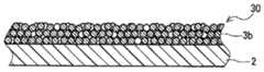
印刷线路板用基材的制造方法包括:通过涂布含有铜颗粒3b的导电性油墨而在基膜2的一个表面上形成涂膜30的涂膜形成步骤;和通过烧结涂膜30而形成包含铜颗粒3b的烧结体3a的金属层3的金属层形成步骤。The method of manufacturing a base material for a printed wiring board includes: a coating film forming step of forming a
在印刷线路板用基材的制造方法中,对金属层3中距金属层3与基膜2的界面100nm以下的区域中的每单位面积的含量进行调节,使得Cr<0.1mg/m2并且Ni<0.1mg/m2。此外,在印刷线路板用基材的制造方法中,将基膜2的层叠有金属层3的表面的算术平均粗糙度(Sa)控制为小于0.10μm。根据印刷线路板用基材的制造方法,可以制造能够容易地形成精细线路的上述印刷线路板用基材1。应当注意,在涂膜形成步骤之前,印刷线路板用基材的制造方法可还包括对基膜2的一个表面(待形成涂膜30的表面)施加亲水化处理的亲水化处理步骤。亲水化处理步骤中的亲水化处理方法的实例包括:通过等离子体照射使基膜2的一个表面亲水化的等离子体处理、或通过碱性溶液使基膜2的一个表面亲水化的碱处理。此外,在印刷线路板用基材的制造方法中,在涂膜形成步骤之前,可以将湿喷装置、喷砂处理等施用于基膜2的一个表面,使得算术平均粗糙度(Sa)在上述范围内。In the manufacturing method of the base material for printed wiring boards, the content per unit area in the region of the
(涂膜形成步骤)(coating film forming step)
在涂膜形成步骤中,如图4A所示,将包含铜颗粒3b的导电性油墨涂布到基膜2的一个表面上,并且使导电性油墨干燥以形成涂膜30。应当注意,涂膜30可以包含导电性油墨的分散介质等。In the coating film forming step, as shown in FIG. 4A , conductive ink containing
<铜颗粒><copper particles>
可以通过高温处理、液相还原法、气相法等来制造待分散在导电性油墨中的铜颗粒3b。其中,根据液相还原法,可以进一步降低制造成本,并且可以通过在水溶液等中搅拌而容易使铜颗粒3b的粒径均匀。The
为了通过液相还原法制造铜颗粒3b,例如,将分散剂以及作为形成铜颗粒3b的铜离子来源的水溶性金属化合物溶解在水中,并添加还原剂,从而使与铜离子的还原反应进行一定的时间。通过液相还原法制造的铜颗粒3b具有均匀的球状或颗粒形状,并且可以是微细颗粒。作为成为铜离子来源的水溶性铜化合物,例如,可以使用硝酸铜(II)(Cu(NO3)2)、五水合硫酸铜(II)(CuSO4·5H2O)等。In order to manufacture the
作为还原剂,可以使用能够在液相(水溶液)的反应体系中还原并析出铜离子的各种还原剂。还原剂的实例包括硼氢化钠、次磷酸钠、肼、诸如三价钛离子和二价钴离子之类的过渡金属离子、抗坏血酸、诸如葡萄糖和果糖之类的还原糖、诸如乙二醇和甘油之类的多元醇等。其中,三价钛离子优选作为还原剂。应当注意,使用三价钛离子作为还原剂的液相还原法称为钛氧化还原法。在钛氧化还原法中,当三价钛离子被氧化成四价钛离子时,铜离子通过氧化还原作用被还原,从而使铜颗粒3b析出。通过钛氧化还原法得到的铜颗粒3b的粒径小且均匀。因此,铜颗粒3b更紧密地堆积,并且涂膜30可以形成为更致密的膜。应当注意,在印刷线路板用基材的制造方法中,例如,通过调节导电性油墨中的钛离子的含量,在所得的印刷基板用基材1中,可以将金属层3中距金属层3与基膜2的界面100nm以下的区域中的每单位面积的Ti含量控制在上述范围内。As the reducing agent, various reducing agents capable of reducing and precipitating copper ions in a liquid phase (aqueous solution) reaction system can be used. Examples of reducing agents include sodium borohydride, sodium hypophosphite, hydrazine, transition metal ions such as trivalent titanium ions and divalent cobalt ions, ascorbic acid, reducing sugars such as glucose and fructose, class of polyols, etc. Among them, trivalent titanium ions are preferably used as the reducing agent. It should be noted that a liquid-phase reduction method using trivalent titanium ions as a reducing agent is called a titanium redox method. In the titanium redox method, when trivalent titanium ions are oxidized to tetravalent titanium ions, copper ions are reduced by oxidation-reduction action, so that
为了调节铜颗粒3b的粒径,可以调节铜化合物、分散剂和还原剂的类型和混合比,并且可以调节使金属化合物进行还原反应时的搅拌速率、温度、时间、pH等。反应体系的pH的下限优选为7,反应体系的pH的上限优选为13。通过将反应体系的pH设定在上述范围内,可以得到具有小粒径的铜颗粒3b。此时,通过使用pH调节剂,易于将反应体系的pH调节至上述范围内。可以使用的pH调节剂的实例包括常用的酸和碱,例如盐酸、硫酸、氢氧化钠、碳酸钠和氨。特别地,为了防止周边部件的劣化,优选不包含杂质元素的硝酸和氨,其中杂质元素例如为碱金属、碱土金属、诸如氯之类的卤素元素、硫、磷和硼。In order to adjust the particle size of the
铜颗粒3b的平均粒径的下限优选为10nm,更优选为15nm。另一方面,铜颗粒3b的平均粒径的上限优选为40nm,更优选为35nm。当铜颗粒3b的平均粒径小于上述下限时,铜颗粒3b在油墨中的分散性和稳定性可能会降低。相反,当铜颗粒3b的平均粒径超过上述上限时,则铜颗粒3b可能容易析出,并且在涂布导电性油墨时,铜颗粒3b的密度可能不均匀。应当注意的是,“平均粒径”是指以分散液中的铜颗粒的粒径分布的体积中心直径D50表示的平均粒径。The lower limit of the average particle diameter of the
导电性油墨中的铜颗粒3b的含有率的下限优选为5质量%,更优选为10质量%,进一步优选为20质量%。另外,导电性油墨中的铜颗粒3b的含有率的上限优选为50质量%,更优选为40质量%,进一步优选为30质量%。通过将铜颗粒3b的含有率设定为下限值以上,能够将涂膜30形成为更致密的膜。另一方面,当铜颗粒3b的含有率超过上限时,涂膜32的膜厚可能会不均匀。The lower limit of the content of
<其他成分><other ingredients>
导电性油墨除了包含铜颗粒3b以外,还可包含分散剂。作为分散剂,可以使用能够使铜颗粒3b很好地分散的各种分散剂,对其没有特别的限制。The conductive ink may contain a dispersant in addition to the
为了防止周边部件的劣化,分散剂优选不包含硫、磷、硼、卤素和碱。分子量在下述范围内的分散剂的优选实例包括:胺系高分子分散剂,例如聚乙烯亚胺和聚乙烯吡咯烷酮;分子中具有羧酸基团的烃系高分子分散剂,例如聚丙烯酸和羧甲基纤维素;具有极性基团的高分子分散剂,例如Poval(聚乙烯醇)、苯乙烯-马来酸共聚物、烯烃-马来酸共聚物,以及在一个分子中具有聚乙烯亚胺部分和聚环氧乙烷部分的共聚物。In order to prevent deterioration of peripheral components, the dispersant preferably does not contain sulfur, phosphorus, boron, halogen and alkali. Preferable examples of dispersants with molecular weights within the following ranges include: amine-based polymer dispersants such as polyethyleneimine and polyvinylpyrrolidone; hydrocarbon-based polymer dispersants having carboxylic acid groups in the molecule, such as polyacrylic acid and carboxyl Methyl cellulose; polymer dispersants with polar groups, such as Poval (polyvinyl alcohol), styrene-maleic acid copolymers, olefin-maleic acid copolymers, and polyethylene glycol in one molecule Copolymers of amine moieties and polyethylene oxide moieties.
分散剂的分子量的下限优选为2,000,并且分散剂的分子量的上限优选为54,000。通过使用分子量在上述范围内的分散剂,可以将铜颗粒3b令人满意地分散在导电性油墨中,并且可以使涂膜30的膜质量致密且无缺陷。当分散剂的分子量小于上述下限值时,可能无法充分获得抑制铜颗粒3b的聚集从而维持分散的效果。相反,当分散剂的分子量超过上述上限时,分散剂的体积可能变得过大,并且在烧结涂膜30时,可能会抑制铜颗粒3b的烧结并且可能产生空隙。此外,当分散剂的体积过大时,涂膜30的密度会降低,且分散剂的分解残留物可能会降低导电性。The lower limit of the molecular weight of the dispersant is preferably 2,000, and the upper limit of the molecular weight of the dispersant is preferably 54,000. By using a dispersant with a molecular weight within the above range, the
也可以将分散剂以溶解于水或水溶性有机溶剂中的溶液状态添加到导电性油墨中。在导电性油墨中混合有分散剂的情况下,相对于100质量份的铜颗粒3b,分散剂的含有率的下限优选为1质量份。相对于100质量份的铜颗粒3b,分散剂的含有率的上限优选为60质量份。当分散剂的含有率小于下限时,防止铜颗粒3b聚集的效果可能不足。相反,当分散剂的含有率超过上限时,在烧结涂膜30时,过量的分散剂可能会抑制铜颗粒3b的烧结并且可能会产生空隙。此外,分散剂的分解残余物可能作为杂质残留在烧结体3a中,从而降低导电性。The dispersant may also be added to the conductive ink in a solution state dissolved in water or a water-soluble organic solvent. When the conductive ink is mixed with a dispersant, the lower limit of the content of the dispersant is preferably 1 part by mass relative to 100 parts by mass of the
例如,水可以用作导电性油墨中的分散介质。在分散介质为水的情况下,相对于100质量份的铜颗粒3b,水的含有率的下限优选为20质量份。另外,相对于100质量份的铜颗粒3b,水的含有率的上限优选为1,900质量份。尽管作为分散介质的水起到(例如)使分散剂充分溶胀并令人满意地分散被分散剂包围的铜颗粒3b的作用,但是当水的含有率低于下限时,分散剂的溶胀效果可能不足。另一方面,当水的含有率超过上限时,导电性油墨中的铜颗粒3b的含有率降低,可能会无法形成具有所需的厚度和密度的良好的金属层3。For example, water can be used as a dispersion medium in conductive inks. When the dispersion medium is water, the lower limit of the water content is preferably 20 parts by mass relative to 100 parts by mass of the
应当注意,在通过液相还原法制造铜颗粒3b的情况下,可以通过使用经过过滤、洗涤、干燥、粉碎等步骤而制成粉末的导电性油墨来制备在液相反应体系(水溶液)中析出的铜颗粒3b。在这种情况下,可以预定比例混合粉末状铜颗粒3b、作为分散介质的水等、任选的分散剂和水溶性有机溶剂,以制备包含铜颗粒3b的导电性油墨。此时,优选使用其中已经析出有铜颗粒3b的液相(水溶液)作为起始材料来制备导电性油墨。具体而言,对包含析出的铜颗粒3b的液相(水溶液)进行处理,例如超滤、离心分离、用水洗涤或电渗析,以除去杂质,并且任选地进行浓缩以除去水。或者,在添加水以调节铜3b颗粒的浓度之后,任选地以预定比例进一步添加水溶性有机溶剂,从而制备包含铜颗粒3b的导电性油墨。通过该方法,可以防止在铜颗粒3b干燥时由于聚集而生成不规则的粗大颗粒,并且容易形成致密且均匀的烧结体3a。It should be noted that in the case of producing the
<导电性油墨的涂布方法><Method of Coating Conductive Ink>
作为将分散有铜颗粒3b的导电性油墨涂布在基膜2的一个表面上的方法,可以使用旋涂法、喷涂法、棒涂法、模涂法、狭缝涂布法、辊涂法或浸涂法等已知的涂布方法。此外,可以通过丝网印刷或利用分配器等将导电性油墨仅涂布在基膜2的一个表面中的一部分上。在涂布导电性油墨之后,例如通过在大于或等于室温的温度下干燥来形成涂膜30。干燥温度的上限优选为100℃,并且更优选为40℃。当干燥温度超过上述上限时,由于涂膜30的快速干燥,在涂膜30中可能出现裂纹。As a method of coating the conductive ink in which the
(金属层形成步骤)(Metal layer forming step)
在金属层形成步骤中,如图4B所示,通过烧结涂膜30形成包含铜颗粒3b的烧结体3a的金属层3。In the metal layer forming step, as shown in FIG. 4B , the
<烧结><sintering>
通过烧结,铜颗粒3b彼此烧结,并且烧结体3a固着在基膜2的一个表面上。应该注意的是,导电性油墨中可能包含的大部分分散剂和其他有机物质会因烧结而挥发或分解。另外,在烧结体3a与基膜2的界面附近,由于铜颗粒3b通过烧结而被氧化,因此在抑制了基于铜颗粒3b的氢氧化铜以及来源于氢氧化铜的基团的生成的同时,生成了基于铜颗粒3b的氧化铜和来源于该氧化铜的基团。在烧结体3a与基膜2的界面附近产生的氧化铜和来源于氧化铜的基团牢固地接合到构成基膜2的树脂如聚酰亚胺上,因此基膜2和烧结体3a之间的密着力增加。By sintering,
为了促进烧结体3a与基膜2的界面附近的铜颗粒3b的氧化,优选在含有一定量的氧的气氛中进行烧结。在这种情况中,烧结气氛中的氧浓度的下限优选为1体积ppm,更优选为10体积ppm。另一方面,氧浓度的上限优选为10,000体积ppm,更优选为1,000体积ppm。当氧浓度低于下限时,在烧结体3a与基膜2的界面附近产生的氧化铜和来源于氧化铜的基团的量可能减少,并且不能充分地增强基膜2和烧结体3a之间的密着力。相反,当氧浓度超过上限时,铜颗粒3b可能被过度氧化,并且烧结体3a的导电性可能会降低。In order to promote the oxidation of the
烧结温度的下限优选为150℃,并且更优选为200℃。另一方面,烧结温度的上限优选为500℃,更优选为400℃。当烧结温度低于下限时,在烧结体3a与基膜2的界面附近产生的氧化铜和来源于氧化铜的基团的量可能减少,并且可能不能充分增强基膜2和烧结体3a之间的密着力。相反,当烧结温度超过上限时,基膜2可能变形。应当注意,对于烧结时间没有特别的限制,但是例如可以在30分钟以上600分钟以下的范围内。The lower limit of the sintering temperature is preferably 150°C, and more preferably 200°C. On the other hand, the upper limit of the sintering temperature is preferably 500°C, more preferably 400°C. When the sintering temperature is lower than the lower limit, the amount of copper oxide and groups derived from copper oxide generated near the interface between the
在印刷线路板用基材的制造方法中,可以通过上述的涂膜形成步骤和金属层形成步骤来制造图1中的印刷线路板用基材1。同时,根据印刷线路板用基材的制造方法,如图4C所示,通过包括将电镀层13b层叠在由图4B的金属层3制成的晶种层13a的外表面上的电镀层层叠步骤,可以制造上述图2所示的印刷线路板用基材11。在印刷线路板用基材的制造方法中,通过包括电镀层层叠步骤,可以增加金属层13的厚度并且可以减小金属层13的电阻。因此,印刷线路板用基材的制造方法适合作为制造用于(例如)射频信号处理用印刷线路板的印刷线路板用基材的方法。In the manufacturing method of the base material for printed wiring boards, the base material 1 for printed wiring boards in FIG. 1 can be manufactured through the above-mentioned coating film formation process and metal layer formation process. Meanwhile, according to the manufacturing method of a base material for a printed wiring board, as shown in FIG. 4C , by including the plating layer lamination step of laminating the
(电镀层层叠步骤)(Electroplating Layer Lamination Step)
在电镀层层叠步骤中,通过电镀铜,从而将电镀层13b层叠在晶种层13a的外表面上。在电镀层层叠步骤中,优选通过使用具有尽可能少的异种金属的催化剂和镀液来形成电镀层13b,以便不影响晶种层13a中距晶种层13a与基膜2的界面100nm以下的区域中的各种不同金属成分的含量。对于电镀层层叠步骤的过程没有特别的限制,例如,可以从公知的铜电镀浴和电镀条件中适当选择。In the plating layer lamination step, the
<印刷线路板的制造方法><Manufacturing method of printed wiring board>
接下来,将参照图5描述根据本公开的印刷线路板的制造方法的一个实施方案。此处,将描述使用图2的印刷线路板用基材11来制造图3的印刷线路板21的方法。印刷线路板的制造方法包括通过将诸如抗蚀剂图案之类的掩模施加至金属层13而进行蚀刻的蚀刻步骤。Next, an embodiment of a method of manufacturing a printed wiring board according to the present disclosure will be described with reference to FIG. 5 . Here, a method of manufacturing the printed
(蚀刻步骤)(etching step)
在蚀刻步骤中,优选通过单次蚀刻去除晶种层13a的位于导电图案22之间的部分。在印刷线路板的制造方法中,因为在所使用的印刷线路板用基材11中,在晶种层13a中距晶种层13a与基膜2的界面100nm以下的区域中每单位面积的Cr和Ni的含量在上述范围内,所以不需要另外进行铜以外的金属的蚀刻。根据该印刷线路板的制造方法,通过蚀刻步骤,可以容易地形成精细线路。In the etching step, the portion of the
[其他实施方案][Other implementations]
以上公开的实施方案在所有方面均应视为示例性的,而不是限制性的。本发明的范围不限于上述实施方案的构成,而是由权利要求书指示,并且意图包括与权利要求书等同的含义和范围内的所有改变。The embodiments disclosed above are to be considered in all respects as illustrative and not restrictive. The scope of the present invention is not limited to the configuration of the above-described embodiments but is indicated by the claims, and is intended to include all changes within the meaning and range equivalent to the claims.
例如,在印刷线路板用基材中,可以不仅在基膜的一个表面上形成金属层,而是可以在基膜的两个表面上层叠金属层。For example, in a base material for a printed wiring board, a metal layer may be formed not only on one surface of a base film but may be laminated on both surfaces of the base film.
如上所述,优选的是,金属层包含固定在基膜上的铜颗粒的烧结体。然而,只要金属层中距金属层与基膜的界面100nm以下的区域中每单位面积的Cr和Ni的含量在上述范围内,则金属层可以不必一定包含固定在基膜上的铜颗粒的烧结体。As described above, it is preferable that the metal layer comprises a sintered body of copper particles fixed on the base film. However, as long as the content of Cr and Ni per unit area in the area below 100 nm from the interface between the metal layer and the base film in the metal layer is within the above range, the metal layer may not necessarily contain sintered copper particles fixed on the base film. body.
印刷线路板用基材不必一定是柔性印刷线路板的基材,而是可以为刚性基材。在这种情况下,基膜的主要成分的实例包括硬质材料,例如酚醛纸、环氧纸、玻璃复合材料、玻璃环氧树脂和玻璃基材;硬质材料和软质材料复合在一起的刚性-柔性材料等。The base material for a printed wiring board does not necessarily have to be a base material of a flexible printed wiring board, and may be a rigid base material. In this case, examples of the main component of the base film include hard materials such as phenolic paper, epoxy paper, glass composite materials, glass epoxy resin, and glass substrates; Rigid-flexible materials, etc.
可以使用例如图1的印刷线路板用基材1形成印刷线路板。印刷线路板还可以包括位于晶种层的外表面上的化学镀层。A printed wiring board can be formed using, for example, the base material 1 for printed wiring boards shown in FIG. 1 . The printed wiring board may also include an electroless plating layer on the outer surface of the seed layer.
尽管在如上所述的实施方案中已经描述了通过减去法形成导电图案的实例,但是用于制造印刷线路板的方法还可以通过半加成方法形成导电图案。Although an example of forming a conductive pattern by a subtractive method has been described in the embodiments described above, the method for manufacturing a printed wiring board can also form a conductive pattern by a semi-additive method.
例子example
尽管下面将参考实施例详细描述本公开,但是本公开不限于这些实施例。Although the present disclosure will be described in detail below with reference to examples, the present disclosure is not limited to these examples.
[实施例][Example]
[No.1][No.1]
将作为还原剂的80g(0.1M)三氯化钛溶液、作为pH调节剂的50g碳酸钠、作为配合剂的90g柠檬酸钠和作为分散剂的1g PEI-PEO接枝共聚物溶解在烧杯中的1升纯水中,将水溶液保持在35℃。另外,向该水溶液中加入保持在相同温度(35℃)的10g(0.04M)硝酸铜三水合物水溶液,进行搅拌以使铜微粒析出。此外,对于通过离心分离的铜微粒,将用200mL的纯水进行水洗的步骤重复两次,并且将铜微粒干燥,然后得到粉末状的铜微粒。铜微粒的平均粒径D50为30nm。随后,通过向粉末状铜微粒中添加纯水以调节浓度,从而制造铜微粒的含有率为30质量%的导电性油墨。此外,通过棒涂法将300μL的导电性油墨涂布在基膜上,从而形成涂膜,其中该基膜由进行了亲水化处理的聚酰亚胺膜(10cm见方)构成。然后,通过在350℃烧结涂膜,形成由铜颗粒的烧结体构成的金属层,从而制备了印刷线路板用基材No.1。用Hitachi High-Tech公司制造的SEM装置“SU8020”测定时,铜颗粒的烧结体的平均粒径为105nm。通过ICP-MS(由Agilent Technologies公司制造的“ICP-MS 7700x”)测定在印刷线路板用基材No.1中,金属层中距金属层与基膜的界面100nm以下的区域中的每单位面积的Cr、Ni、Pd和Ti的含量。另外,以30μm×30μm的测量范围和90的截断值测量基膜的层叠有金属层的表面的算术平均粗糙度(Sa)。测量结果在表1中示出。80g (0.1M) titanium trichloride solution as reducing agent, 50g sodium carbonate as pH regulator, 90g sodium citrate as complexing agent and 1g PEI-PEO graft copolymer as dispersant are dissolved in a beaker 1 liter of pure water, and keep the aqueous solution at 35°C. In addition, 10 g (0.04 M) of copper nitrate trihydrate aqueous solution maintained at the same temperature (35° C.) was added to this aqueous solution, and stirred to deposit copper fine particles. Furthermore, for the copper fine particles separated by centrifugation, the step of washing with 200 mL of pure water was repeated twice, and the copper fine particles were dried, and then powdery copper fine particles were obtained. The average particle diameter D50 of the copper fine particles was 30 nm. Then, the concentration was adjusted by adding pure water to the powdery copper fine particles to manufacture a conductive ink having a copper fine particle content of 30% by mass. In addition, 300 μL of conductive ink was applied by a bar coating method on a base film composed of a polyimide film (10 cm square) subjected to a hydrophilization treatment to form a coating film. Then, the coating film was sintered at 350° C. to form a metal layer composed of a sintered body of copper particles, thereby preparing a substrate No. 1 for a printed wiring board. The average particle diameter of the sintered body of copper particles was 105 nm when measured with SEM apparatus "SU8020" manufactured by Hitachi High-Tech Corporation. In substrate No. 1 for printed wiring boards, in the area of 100 nm or less from the interface between the metal layer and the base film in the metal layer, each unit The content of Cr, Ni, Pd and Ti in the area. In addition, the arithmetic mean roughness (Sa) of the metal layer-laminated surface of the base film was measured with a measurement range of 30 μm×30 μm and a cutoff value of 90. The measurement results are shown in Table 1.
[No.2和No.3][No.2 and No.3]
以与No.1相同的方式制备印刷线路板用基材No.2和No.3,不同之处在于,如表1所示设定铜颗粒的烧结体的平均粒径、金属层中距金属层与基膜的界面100nm以下的区域中的每单位面积的Cr、Ni、Pd和Ti的含量、以及基膜的层叠有金属层的表面的算术平均粗糙度(Sa)。Base materials No.2 and No.3 for printed wiring boards were prepared in the same manner as No.1, except that the average particle diameter of the sintered body of copper particles, the distance between the metal layer and the metal layer were set as shown in Table 1. The content of Cr, Ni, Pd and Ti per unit area in the area below 100 nm of the interface between the layer and the base film, and the arithmetic mean roughness (Sa) of the surface of the base film on which the metal layer is laminated.
[比较例][comparative example]
[No.4][No.4]
通过溅射法在由聚酰亚胺膜(10cm见方)构成的基膜上依次层叠镍铬合金层和铜层,从而制备印刷线路板用基材No.4。对于印刷线路板用基材No.4,表1中示出了通过与上述相同的方法测定的金属层中距金属层与基膜的界面100nm以下的区域中的每单位面积的Cr、Ni、Pd和Ti的含量,以及基膜的层叠有金属层的表面的算术平均粗糙度(Sa)的测定结果。A nichrome layer and a copper layer were sequentially laminated on a base film composed of a polyimide film (10 cm square) by a sputtering method to prepare a substrate No. 4 for a printed wiring board. For substrate No. 4 for printed wiring boards, in Table 1, Cr, Ni, Ni, Ni, The content of Pd and Ti, and the measurement results of the arithmetic mean roughness (Sa) of the surface of the base film on which the metal layer is laminated.
[No.5][No.5]
通过经由粘合剂层将铜箔层叠在由聚酰亚胺膜(10cm见方)制成的基膜上,从而制备印刷线路板用基材No.5,其中在基膜的一个表面上层叠了由铜箔制成的金属层。对于印刷线路板用基材No.5,表1中示出了通过与上述相同的方法测定的金属层中距金属层与基膜的界面(金属层的基膜侧的界面)100nm以下的区域中的每单位面积的Cr、Ni、Pd和Ti的含量,以及基膜的层叠有金属层的表面的算术平均粗糙度(Sa)的测定结果。Substrate No. 5 for printed wiring boards was prepared by laminating copper foil on a base film made of polyimide film (10 cm square) via an adhesive layer, in which on one surface of the base film laminated A metal layer made of copper foil. For substrate No. 5 for printed wiring boards, Table 1 shows the region of 100 nm or less from the interface between the metal layer and the base film (the interface on the base film side of the metal layer) in the metal layer measured by the same method as above. The content of Cr, Ni, Pd, and Ti per unit area in , and the measurement results of the arithmetic mean roughness (Sa) of the surface of the base film on which the metal layer is laminated.
[No.6][No.6]
通过溅射法在由聚酰亚胺膜(10cm见方)构成的基膜上依次层叠镍铬合金层和铜层,从而制备印刷线路板用基材No.6。对于印刷线路板用基材No.6,表1中示出了通过与上述相同的方法测定的金属层中距金属层与基膜的界面100nm以下的区域中的每单位面积的Cr、Ni、Pd和Ti的含量,以及基膜的层叠有金属层的表面的算术平均粗糙度(Sa)的测定结果。A nichrome layer and a copper layer were sequentially laminated on a base film composed of a polyimide film (10 cm square) by a sputtering method to prepare a substrate No. 6 for a printed wiring board. For substrate No. 6 for printed wiring boards, in Table 1, Cr, Ni, Ni, Ni, The content of Pd and Ti, and the measurement results of the arithmetic mean roughness (Sa) of the surface of the base film on which the metal layer is laminated.
[No.7][No.7]
以与No.1相同的方式制备印刷线路板用基材No.7,不同之处在于,如表1所示设定铜颗粒的烧结体的平均粒径、金属层中距金属层与基膜的界面100nm以下的区域中的每单位面积的Cr、Ni、Pd和Ti的含量、以及基膜的层叠有金属层的表面的算术平均粗糙度(Sa)。Base material No. 7 for printed wiring boards was prepared in the same manner as No. 1, except that the average particle diameter of the sintered body of copper particles, the distance between the metal layer and the base film were set as shown in Table 1. The contents of Cr, Ni, Pd, and Ti per unit area in the region below 100 nm of the interface, and the arithmetic mean roughness (Sa) of the surface of the base film on which the metal layer is laminated.
<精细线路的形成性><Formation of fine lines>
对于No.1至No.7中的每一个,通过将抗蚀剂图案施加至印刷线路板用基材的金属层的表面,以使L/S(线&间距)=10μm/10μm,从而进行蚀刻。具体而言,将其浸入1重量%的十二烷基硫酸钠水溶液中,然后将其浸入CA5330(由MEC COMPANY LTD制造)中。蚀刻结果示于表1。应注意,在表1中,“A”表示形成了L/S=10μm/10μm的线路,而“B”表示没有形成“L/S=10μm/10μm”的线路。For each of No.1 to No.7, by applying a resist pattern to the surface of the metal layer of the substrate for printed wiring boards so that L/S (line & space) = 10 μm/10 μm, etch. Specifically, it was immersed in a 1% by weight aqueous solution of sodium lauryl sulfate, and then it was immersed in CA5330 (manufactured by MEC COMPANY LTD). The etching results are shown in Table 1. It should be noted that in Table 1, "A" indicates that a line of L/S = 10 µm/10 µm was formed, and "B" indicates that a line of "L/S = 10 µm/10 µm" was not formed.
[表1][Table 1]

<评估结果><evaluation result>
如表1所示,在印刷线路板用基材No.1至No.3中,金属层中距金属层与基膜的界面100nm以下的区域中的每单位面积的Cr和Ni的含量在上述范围内,并且基膜的层叠有金属层的表面的算术平均粗糙度(Sa)为上述值。因此,可以高精度地进行金属层的蚀刻,其结果是,可以形成精细线路。另一方面,在印刷线路板用基材No.4和No.6中,金属层中距金属层与基膜的界面100nm以下的区域中的每单位面积的Cr和Ni的含量为0.1mg/m2以上,并且在印刷线路板用基材No.5和No.7中,基膜的层叠有金属层的表面的算术平均粗糙度(Sa)为0.10μm以上。因此,蚀刻是困难的,并且不能进行高精度的蚀刻,并且不能形成精细电路。As shown in Table 1, in base materials No. 1 to No. 3 for printed wiring boards, the contents of Cr and Ni per unit area in the region of the metal layer within 100 nm from the interface between the metal layer and the base film are within the above-mentioned range. range, and the arithmetic average roughness (Sa) of the surface of the base film on which the metal layer is laminated is the above value. Therefore, the metal layer can be etched with high precision, and as a result, fine lines can be formed. On the other hand, in base materials No. 4 and No. 6 for printed wiring boards, the content of Cr and Ni per unit area in the region of 100 nm or less from the interface between the metal layer and the base film in the metal layer was 0.1 mg/ m2 or more, and in substrates No. 5 and No. 7 for printed wiring boards, the arithmetic average roughness (Sa) of the surface of the base film on which the metal layer was laminated was 0.10 μm or more. Therefore, etching is difficult, and high-precision etching cannot be performed, and fine circuits cannot be formed.
附图标记说明Explanation of reference signs
1,11 印刷线路板用基材1,11 Substrates for printed circuit boards
2 基膜2 basement membrane
3、13 金属层3, 13 metal layers
3a 烧结体3a Sintered body
3b 铜颗粒3b copper particles
13a 晶种层13a Seed layer
13b 电镀层13b Plating layer
21 印刷线路板21 printed circuit board
22 导电图案22 conductive patterns
30 涂膜30 film
Claims (8)
Applications Claiming Priority (3)
| Application Number | Priority Date | Filing Date | Title |
|---|---|---|---|
| JP2017-247550 | 2017-12-25 | ||
| JP2017247550AJP7032127B2 (en) | 2017-12-25 | 2017-12-25 | Method for manufacturing printed wiring board base material, printed wiring board and printed wiring board base material |
| PCT/JP2018/035236WO2019130690A1 (en) | 2017-12-25 | 2018-09-24 | Printed circuit board substrate and printed circuit board |
Publications (2)
| Publication Number | Publication Date |
|---|---|
| CN111512710A CN111512710A (en) | 2020-08-07 |
| CN111512710Btrue CN111512710B (en) | 2023-06-16 |
Family
ID=67063372
Family Applications (1)
| Application Number | Title | Priority Date | Filing Date |
|---|---|---|---|
| CN201880083383.XAActiveCN111512710B (en) | 2017-12-25 | 2018-09-24 | Substrates for printed wiring boards and printed wiring boards |
Country Status (4)
| Country | Link |
|---|---|
| US (1) | US11013113B2 (en) |
| JP (1) | JP7032127B2 (en) |
| CN (1) | CN111512710B (en) |
| WO (1) | WO2019130690A1 (en) |
Families Citing this family (3)
| Publication number | Priority date | Publication date | Assignee | Title |
|---|---|---|---|---|
| US20230371176A1 (en)* | 2020-10-09 | 2023-11-16 | Sumitomo Electric Industries, Ltd. | Base material for printed circuit, printed circuit, and method of manufacturing base material for printed circuit |
| CN118044340A (en)* | 2022-03-29 | 2024-05-14 | 住友电气工业株式会社 | Substrate for printed wiring board and printed wiring board |
| TWI842105B (en)* | 2022-09-26 | 2024-05-11 | 國立清華大學 | Method of fabricating electronic circuit and metal ion solution |
Citations (4)
| Publication number | Priority date | Publication date | Assignee | Title |
|---|---|---|---|---|
| JP2006303171A (en)* | 2005-04-20 | 2006-11-02 | Teijin Ltd | Substrate for flexible printed circuit |
| JP2006310360A (en)* | 2005-04-26 | 2006-11-09 | Teijin Ltd | Substrate for flexible printed circuit |
| CN101996891A (en)* | 2009-08-18 | 2011-03-30 | 住友金属矿山株式会社 | Metal-coated polyimide film and process for producing the same |
| JP2016152405A (en)* | 2015-02-19 | 2016-08-22 | 住友電工プリントサーキット株式会社 | Base material for printed wiring board, printed wiring board and method of producing base material for printed wiring board |
Family Cites Families (5)
| Publication number | Priority date | Publication date | Assignee | Title |
|---|---|---|---|---|
| JPWO2003103352A1 (en)* | 2002-06-04 | 2005-10-06 | 住友電気工業株式会社 | Printed wiring board, printed wiring board and manufacturing method thereof |
| KR100701645B1 (en)* | 2004-08-02 | 2007-03-30 | 도레이새한 주식회사 | Manufacturing method of laminated structure for flexible circuit board |
| JP4948199B2 (en)* | 2007-02-16 | 2012-06-06 | 旭化成イーマテリアルズ株式会社 | Manufacturing method of laminate |
| JP2010219075A (en)* | 2009-03-12 | 2010-09-30 | Dainippon Printing Co Ltd | Printed wiring board and method of manufacturing the same |
| JP6675989B2 (en) | 2014-12-25 | 2020-04-08 | 住友電気工業株式会社 | Printed wiring board substrate, printed wiring board, and method for manufacturing printed wiring board substrate |
- 2017
- 2017-12-25JPJP2017247550Apatent/JP7032127B2/enactiveActive
- 2018
- 2018-09-24USUS16/955,351patent/US11013113B2/enactiveActive
- 2018-09-24CNCN201880083383.XApatent/CN111512710B/enactiveActive
- 2018-09-24WOPCT/JP2018/035236patent/WO2019130690A1/ennot_activeCeased
Patent Citations (4)
| Publication number | Priority date | Publication date | Assignee | Title |
|---|---|---|---|---|
| JP2006303171A (en)* | 2005-04-20 | 2006-11-02 | Teijin Ltd | Substrate for flexible printed circuit |
| JP2006310360A (en)* | 2005-04-26 | 2006-11-09 | Teijin Ltd | Substrate for flexible printed circuit |
| CN101996891A (en)* | 2009-08-18 | 2011-03-30 | 住友金属矿山株式会社 | Metal-coated polyimide film and process for producing the same |
| JP2016152405A (en)* | 2015-02-19 | 2016-08-22 | 住友電工プリントサーキット株式会社 | Base material for printed wiring board, printed wiring board and method of producing base material for printed wiring board |
Also Published As
| Publication number | Publication date |
|---|---|
| WO2019130690A1 (en) | 2019-07-04 |
| US11013113B2 (en) | 2021-05-18 |
| US20210022245A1 (en) | 2021-01-21 |
| JP2019114681A (en) | 2019-07-11 |
| JP7032127B2 (en) | 2022-03-08 |
| CN111512710A (en) | 2020-08-07 |
Similar Documents
| Publication | Publication Date | Title |
|---|---|---|
| CN102415222B (en) | Substrate for printed wiring board, printed wiring board, and methods for producing same | |
| JP2020057799A (en) | Printed wiring board substrate, printed wiring board, method for manufacturing printed wiring board, and method for manufacturing printed wiring board | |
| JP6400503B2 (en) | Printed wiring board substrate and printed wiring board | |
| JP6484218B2 (en) | Printed wiring board substrate and printed wiring board | |
| CN107211537A (en) | The manufacture method of printed substrate base material, printed substrate and printed substrate | |
| US10292265B2 (en) | Substrate for printed circuit board, printed circuit board, and method for producing substrate for printed circuit board | |
| US10237976B2 (en) | Substrate for printed circuit board, printed circuit board, and method for producing substrate for printed circuit board | |
| CN111512710B (en) | Substrates for printed wiring boards and printed wiring boards | |
| WO2019077815A1 (en) | Base material for printed wiring board, and printed wiring board | |
| JP6466110B2 (en) | Printed wiring board substrate, printed wiring board, and printed wiring board manufacturing method | |
| JP6484026B2 (en) | Printed wiring board substrate, printed wiring board, and printed wiring board manufacturing method | |
| JP2017073415A (en) | Substrate for printed wiring board, printed wiring board and electronic component | |
| CN111886937A (en) | Substrate for printed circuit board, printed circuit board, method for manufacturing substrate for printed circuit board, and copper nano-ink | |
| US10842027B2 (en) | Base material for printed circuit board and printed circuit board | |
| WO2016104391A1 (en) | Substrate for printed wiring board, printed wiring board, and method for producing substrate for printed wiring board | |
| CN111512709B (en) | Substrate for printed wiring board and printed wiring board | |
| JP5327107B2 (en) | Printed wiring board substrate, printed wiring board, and printed wiring board manufacturing method | |
| JP6473018B2 (en) | Method for manufacturing substrate for printed wiring board, substrate for printed wiring board and printed wiring board | |
| WO2019225269A1 (en) | Printed circuit board substrate and printed circuit board |
Legal Events
| Date | Code | Title | Description |
|---|---|---|---|
| PB01 | Publication | ||
| PB01 | Publication | ||
| SE01 | Entry into force of request for substantive examination | ||
| SE01 | Entry into force of request for substantive examination | ||
| GR01 | Patent grant | ||
| GR01 | Patent grant |