CN111512356A - Display device - Google Patents
Display deviceDownload PDFInfo
- Publication number
- CN111512356A CN111512356ACN201880083528.6ACN201880083528ACN111512356ACN 111512356 ACN111512356 ACN 111512356ACN 201880083528 ACN201880083528 ACN 201880083528ACN 111512356 ACN111512356 ACN 111512356A
- Authority
- CN
- China
- Prior art keywords
- display device
- insulating film
- channel
- oxide semiconductor
- film
- Prior art date
- Legal status (The legal status is an assumption and is not a legal conclusion. Google has not performed a legal analysis and makes no representation as to the accuracy of the status listed.)
- Granted
Links
Images


Classifications
- G—PHYSICS
- G02—OPTICS
- G02F—OPTICAL DEVICES OR ARRANGEMENTS FOR THE CONTROL OF LIGHT BY MODIFICATION OF THE OPTICAL PROPERTIES OF THE MEDIA OF THE ELEMENTS INVOLVED THEREIN; NON-LINEAR OPTICS; FREQUENCY-CHANGING OF LIGHT; OPTICAL LOGIC ELEMENTS; OPTICAL ANALOGUE/DIGITAL CONVERTERS
- G02F1/00—Devices or arrangements for the control of the intensity, colour, phase, polarisation or direction of light arriving from an independent light source, e.g. switching, gating or modulating; Non-linear optics
- G02F1/01—Devices or arrangements for the control of the intensity, colour, phase, polarisation or direction of light arriving from an independent light source, e.g. switching, gating or modulating; Non-linear optics for the control of the intensity, phase, polarisation or colour
- G02F1/13—Devices or arrangements for the control of the intensity, colour, phase, polarisation or direction of light arriving from an independent light source, e.g. switching, gating or modulating; Non-linear optics for the control of the intensity, phase, polarisation or colour based on liquid crystals, e.g. single liquid crystal display cells
- G02F1/133—Constructional arrangements; Operation of liquid crystal cells; Circuit arrangements
- G02F1/136—Liquid crystal cells structurally associated with a semi-conducting layer or substrate, e.g. cells forming part of an integrated circuit
- G02F1/1362—Active matrix addressed cells
- G02F1/1368—Active matrix addressed cells in which the switching element is a three-electrode device
- G02F1/13685—Top gates
- G—PHYSICS
- G09—EDUCATION; CRYPTOGRAPHY; DISPLAY; ADVERTISING; SEALS
- G09F—DISPLAYING; ADVERTISING; SIGNS; LABELS OR NAME-PLATES; SEALS
- G09F9/00—Indicating arrangements for variable information in which the information is built-up on a support by selection or combination of individual elements
- G09F9/30—Indicating arrangements for variable information in which the information is built-up on a support by selection or combination of individual elements in which the desired character or characters are formed by combining individual elements
- H—ELECTRICITY
- H10—SEMICONDUCTOR DEVICES; ELECTRIC SOLID-STATE DEVICES NOT OTHERWISE PROVIDED FOR
- H10D—INORGANIC ELECTRIC SEMICONDUCTOR DEVICES
- H10D30/00—Field-effect transistors [FET]
- H10D30/60—Insulated-gate field-effect transistors [IGFET]
- H10D30/67—Thin-film transistors [TFT]
- H10D30/6704—Thin-film transistors [TFT] having supplementary regions or layers in the thin films or in the insulated bulk substrates for controlling properties of the device
- H10D30/6723—Thin-film transistors [TFT] having supplementary regions or layers in the thin films or in the insulated bulk substrates for controlling properties of the device having light shields
- H—ELECTRICITY
- H10—SEMICONDUCTOR DEVICES; ELECTRIC SOLID-STATE DEVICES NOT OTHERWISE PROVIDED FOR
- H10D—INORGANIC ELECTRIC SEMICONDUCTOR DEVICES
- H10D30/00—Field-effect transistors [FET]
- H10D30/60—Insulated-gate field-effect transistors [IGFET]
- H10D30/67—Thin-film transistors [TFT]
- H10D30/6729—Thin-film transistors [TFT] characterised by the electrodes
- H10D30/673—Thin-film transistors [TFT] characterised by the electrodes characterised by the shapes, relative sizes or dispositions of the gate electrodes
- H—ELECTRICITY
- H10—SEMICONDUCTOR DEVICES; ELECTRIC SOLID-STATE DEVICES NOT OTHERWISE PROVIDED FOR
- H10D—INORGANIC ELECTRIC SEMICONDUCTOR DEVICES
- H10D30/00—Field-effect transistors [FET]
- H10D30/60—Insulated-gate field-effect transistors [IGFET]
- H10D30/67—Thin-film transistors [TFT]
- H10D30/6729—Thin-film transistors [TFT] characterised by the electrodes
- H10D30/6737—Thin-film transistors [TFT] characterised by the electrodes characterised by the electrode materials
- H10D30/6739—Conductor-insulator-semiconductor electrodes
- H—ELECTRICITY
- H10—SEMICONDUCTOR DEVICES; ELECTRIC SOLID-STATE DEVICES NOT OTHERWISE PROVIDED FOR
- H10D—INORGANIC ELECTRIC SEMICONDUCTOR DEVICES
- H10D30/00—Field-effect transistors [FET]
- H10D30/60—Insulated-gate field-effect transistors [IGFET]
- H10D30/67—Thin-film transistors [TFT]
- H10D30/674—Thin-film transistors [TFT] characterised by the active materials
- H10D30/6755—Oxide semiconductors, e.g. zinc oxide, copper aluminium oxide or cadmium stannate
- H—ELECTRICITY
- H10—SEMICONDUCTOR DEVICES; ELECTRIC SOLID-STATE DEVICES NOT OTHERWISE PROVIDED FOR
- H10D—INORGANIC ELECTRIC SEMICONDUCTOR DEVICES
- H10D64/00—Electrodes of devices having potential barriers
- H10D64/01—Manufacture or treatment
- H—ELECTRICITY
- H10—SEMICONDUCTOR DEVICES; ELECTRIC SOLID-STATE DEVICES NOT OTHERWISE PROVIDED FOR
- H10D—INORGANIC ELECTRIC SEMICONDUCTOR DEVICES
- H10D86/00—Integrated devices formed in or on insulating or conducting substrates, e.g. formed in silicon-on-insulator [SOI] substrates or on stainless steel or glass substrates
- H10D86/01—Manufacture or treatment
- H10D86/021—Manufacture or treatment of multiple TFTs
- H10D86/0221—Manufacture or treatment of multiple TFTs comprising manufacture, treatment or patterning of TFT semiconductor bodies
- H—ELECTRICITY
- H10—SEMICONDUCTOR DEVICES; ELECTRIC SOLID-STATE DEVICES NOT OTHERWISE PROVIDED FOR
- H10D—INORGANIC ELECTRIC SEMICONDUCTOR DEVICES
- H10D86/00—Integrated devices formed in or on insulating or conducting substrates, e.g. formed in silicon-on-insulator [SOI] substrates or on stainless steel or glass substrates
- H10D86/40—Integrated devices formed in or on insulating or conducting substrates, e.g. formed in silicon-on-insulator [SOI] substrates or on stainless steel or glass substrates characterised by multiple TFTs
- H10D86/421—Integrated devices formed in or on insulating or conducting substrates, e.g. formed in silicon-on-insulator [SOI] substrates or on stainless steel or glass substrates characterised by multiple TFTs having a particular composition, shape or crystalline structure of the active layer
- H10D86/423—Integrated devices formed in or on insulating or conducting substrates, e.g. formed in silicon-on-insulator [SOI] substrates or on stainless steel or glass substrates characterised by multiple TFTs having a particular composition, shape or crystalline structure of the active layer comprising semiconductor materials not belonging to the Group IV, e.g. InGaZnO
- H—ELECTRICITY
- H10—SEMICONDUCTOR DEVICES; ELECTRIC SOLID-STATE DEVICES NOT OTHERWISE PROVIDED FOR
- H10D—INORGANIC ELECTRIC SEMICONDUCTOR DEVICES
- H10D86/00—Integrated devices formed in or on insulating or conducting substrates, e.g. formed in silicon-on-insulator [SOI] substrates or on stainless steel or glass substrates
- H10D86/40—Integrated devices formed in or on insulating or conducting substrates, e.g. formed in silicon-on-insulator [SOI] substrates or on stainless steel or glass substrates characterised by multiple TFTs
- H10D86/421—Integrated devices formed in or on insulating or conducting substrates, e.g. formed in silicon-on-insulator [SOI] substrates or on stainless steel or glass substrates characterised by multiple TFTs having a particular composition, shape or crystalline structure of the active layer
- H10D86/425—Integrated devices formed in or on insulating or conducting substrates, e.g. formed in silicon-on-insulator [SOI] substrates or on stainless steel or glass substrates characterised by multiple TFTs having a particular composition, shape or crystalline structure of the active layer having different crystal properties in different TFTs or within an individual TFT
- H—ELECTRICITY
- H10—SEMICONDUCTOR DEVICES; ELECTRIC SOLID-STATE DEVICES NOT OTHERWISE PROVIDED FOR
- H10D—INORGANIC ELECTRIC SEMICONDUCTOR DEVICES
- H10D86/00—Integrated devices formed in or on insulating or conducting substrates, e.g. formed in silicon-on-insulator [SOI] substrates or on stainless steel or glass substrates
- H10D86/40—Integrated devices formed in or on insulating or conducting substrates, e.g. formed in silicon-on-insulator [SOI] substrates or on stainless steel or glass substrates characterised by multiple TFTs
- H10D86/451—Integrated devices formed in or on insulating or conducting substrates, e.g. formed in silicon-on-insulator [SOI] substrates or on stainless steel or glass substrates characterised by multiple TFTs characterised by the compositions or shapes of the interlayer dielectrics
- H—ELECTRICITY
- H10—SEMICONDUCTOR DEVICES; ELECTRIC SOLID-STATE DEVICES NOT OTHERWISE PROVIDED FOR
- H10D—INORGANIC ELECTRIC SEMICONDUCTOR DEVICES
- H10D86/00—Integrated devices formed in or on insulating or conducting substrates, e.g. formed in silicon-on-insulator [SOI] substrates or on stainless steel or glass substrates
- H10D86/40—Integrated devices formed in or on insulating or conducting substrates, e.g. formed in silicon-on-insulator [SOI] substrates or on stainless steel or glass substrates characterised by multiple TFTs
- H10D86/60—Integrated devices formed in or on insulating or conducting substrates, e.g. formed in silicon-on-insulator [SOI] substrates or on stainless steel or glass substrates characterised by multiple TFTs wherein the TFTs are in active matrices
- H—ELECTRICITY
- H10—SEMICONDUCTOR DEVICES; ELECTRIC SOLID-STATE DEVICES NOT OTHERWISE PROVIDED FOR
- H10D—INORGANIC ELECTRIC SEMICONDUCTOR DEVICES
- H10D99/00—Subject matter not provided for in other groups of this subclass
- H—ELECTRICITY
- H10—SEMICONDUCTOR DEVICES; ELECTRIC SOLID-STATE DEVICES NOT OTHERWISE PROVIDED FOR
- H10K—ORGANIC ELECTRIC SOLID-STATE DEVICES
- H10K59/00—Integrated devices, or assemblies of multiple devices, comprising at least one organic light-emitting element covered by group H10K50/00
- H10K59/10—OLED displays
- H10K59/12—Active-matrix OLED [AMOLED] displays
- H10K59/121—Active-matrix OLED [AMOLED] displays characterised by the geometry or disposition of pixel elements
- H10K59/1213—Active-matrix OLED [AMOLED] displays characterised by the geometry or disposition of pixel elements the pixel elements being TFTs
- H—ELECTRICITY
- H10—SEMICONDUCTOR DEVICES; ELECTRIC SOLID-STATE DEVICES NOT OTHERWISE PROVIDED FOR
- H10K—ORGANIC ELECTRIC SOLID-STATE DEVICES
- H10K59/00—Integrated devices, or assemblies of multiple devices, comprising at least one organic light-emitting element covered by group H10K50/00
- H10K59/10—OLED displays
- H10K59/12—Active-matrix OLED [AMOLED] displays
- H10K59/126—Shielding, e.g. light-blocking means over the TFTs
- H—ELECTRICITY
- H01—ELECTRIC ELEMENTS
- H01L—SEMICONDUCTOR DEVICES NOT COVERED BY CLASS H10
- H01L21/00—Processes or apparatus adapted for the manufacture or treatment of semiconductor or solid state devices or of parts thereof
- H01L21/02—Manufacture or treatment of semiconductor devices or of parts thereof
- H01L21/04—Manufacture or treatment of semiconductor devices or of parts thereof the devices having potential barriers, e.g. a PN junction, depletion layer or carrier concentration layer
- H01L21/34—Manufacture or treatment of semiconductor devices or of parts thereof the devices having potential barriers, e.g. a PN junction, depletion layer or carrier concentration layer the devices having semiconductor bodies not provided for in groups H01L21/18, H10D48/04 and H10D48/07, with or without impurities, e.g. doping materials
- H01L21/42—Bombardment with radiation
- H01L21/423—Bombardment with radiation with high-energy radiation
- H01L21/425—Bombardment with radiation with high-energy radiation producing ion implantation
- H01L21/426—Bombardment with radiation with high-energy radiation producing ion implantation using masks
- H—ELECTRICITY
- H10—SEMICONDUCTOR DEVICES; ELECTRIC SOLID-STATE DEVICES NOT OTHERWISE PROVIDED FOR
- H10D—INORGANIC ELECTRIC SEMICONDUCTOR DEVICES
- H10D30/00—Field-effect transistors [FET]
- H10D30/60—Insulated-gate field-effect transistors [IGFET]
- H10D30/67—Thin-film transistors [TFT]
- H10D30/6729—Thin-film transistors [TFT] characterised by the electrodes
- H10D30/673—Thin-film transistors [TFT] characterised by the electrodes characterised by the shapes, relative sizes or dispositions of the gate electrodes
- H10D30/6733—Multi-gate TFTs
- H10D30/6734—Multi-gate TFTs having gate electrodes arranged on both top and bottom sides of the channel, e.g. dual-gate TFTs
Landscapes
- Physics & Mathematics (AREA)
- Nonlinear Science (AREA)
- Engineering & Computer Science (AREA)
- Microelectronics & Electronic Packaging (AREA)
- General Physics & Mathematics (AREA)
- Optics & Photonics (AREA)
- Crystallography & Structural Chemistry (AREA)
- Chemical & Material Sciences (AREA)
- Mathematical Physics (AREA)
- Geometry (AREA)
- Theoretical Computer Science (AREA)
- Thin Film Transistor (AREA)
- Manufacturing & Machinery (AREA)
- Electroluminescent Light Sources (AREA)
- Liquid Crystal (AREA)
- Devices For Indicating Variable Information By Combining Individual Elements (AREA)
Abstract
Description
Translated fromChinese技术领域technical field
本发明涉及显示装置,涉及具有使用氧化物半导体的TFT的显示装置。The present invention relates to a display device, and relates to a display device having a TFT using an oxide semiconductor.
背景技术Background technique
有机EL显示装置在各像素内具有由TFT(Thin Film Transistor:薄膜晶体管)形成的驱动晶体管、开关晶体管,另外,液晶显示装置在各像素内具有由TFT形成的开关晶体管。因此TFT的特性是重要的。The organic EL display device includes a driving transistor and a switching transistor formed of a TFT (Thin Film Transistor) in each pixel, and a liquid crystal display device includes a switching transistor formed of a TFT in each pixel. Therefore, the characteristics of the TFT are important.
氧化物半导体截止电阻(OFF电阻)高,在将其用于TFT时能够减小截止电流(OFF电流)。因此能够减小像素电极电位的变化。另外,使用氧化物半导体的TFT与使用多晶硅等TFT相比能够在更低的温度形成,因此能够实现使用树脂基板而得的显示装置。Oxide semiconductors have high off-resistance (OFF resistance) and can reduce off-current (OFF current) when they are used in TFTs. Therefore, the variation in the potential of the pixel electrode can be reduced. In addition, a TFT using an oxide semiconductor can be formed at a lower temperature than a TFT using polysilicon or the like, and thus a display device using a resin substrate can be realized.
在TFT中,在沟道与漏极之间电场集中,存在在该部分发生绝缘击穿的危险。因此,在使用多晶硅(poly-Si)的TFT中,在沟道与漏极之间形成LDD(Lightly Doped Drain:轻掺杂漏极)区域以防止该部分的绝缘击穿。In a TFT, the electric field is concentrated between the channel and the drain, and there is a risk of dielectric breakdown in this portion. Therefore, in a TFT using polysilicon (poly-Si), an LDD (Lightly Doped Drain: Lightly Doped Drain) region is formed between the channel and the drain to prevent insulation breakdown in this portion.
在使用氧化物半导体的在TFT中,为了形成漏极和源极,通过向氧化物半导体的漏极和源极的部分供给氢而进行对该部分赋予导电性的处理。在专利文献1中记载了下述构成:使供给至漏极及源极的氢扩散,形成发挥与LDD区域相同作用的区域、即在沟道与漏极或源极之间形成电阻比沟道区域小、比漏极或源极大的区域。In a TFT using an oxide semiconductor, in order to form a drain electrode and a source electrode, a process of imparting conductivity to the portion of the drain electrode and the source electrode of the oxide semiconductor is performed by supplying hydrogen to the portion.
现有技术文献prior art literature
专利文献Patent Literature
专利文献1:日本特开2017-85079号公报Patent Document 1: Japanese Patent Laid-Open No. 2017-85079
发明内容SUMMARY OF THE INVENTION
发明要解决的课题The problem to be solved by the invention
如专利文献1记载所示,对于通过退火使氢扩散至栅电极的下侧而形成中间电阻部分的方法而言,难以控制氢的扩散区域。特别是,若沟道长度变小,则存在TFT耗尽(deplete)的危险。若为了减小漏极及源极的电阻而向漏极及源极供给更多的氢,则耗尽的危险进一步增加。As described in
本发明的课题为能够得到下述构成,即,在使用氧化物半导体的TFT中,能够在沟道与漏极及源极之间稳定地形成中间区域。另外,本发明的课题为,实现具有稳定特性的使用氧化物半导体的TFT。An object of the present invention is to obtain a configuration in which an intermediate region can be stably formed between a channel and a drain and a source in a TFT using an oxide semiconductor. Another object of the present invention is to realize a TFT using an oxide semiconductor having stable characteristics.
用于解决课题的手段means of solving problems
本发明能够克服上述问题,具体的手段如下。The present invention can overcome the above problems, and the specific means are as follows.
(1)显示装置,其形成有多个具有由氧化物半导体构成的薄膜晶体管(TFT)的像素,所述显示装置的特征在于,所述氧化物半导体中形成有沟道,在所述沟道的两侧形成有漏极及源极,在所述沟道与所述漏极之间及所述沟道与所述源极之间形成有中间区域,在所述氧化物半导体的所述沟道与所述中间区域之上形成有栅极绝缘膜,在所述栅极绝缘膜之上形成有氧化铝膜,在所述沟道的上方且在所述氧化铝膜之上形成有栅电极,在所述栅电极的两侧形成有侧壁间隔件,以覆盖所述栅电极、所述侧壁间隔件及所述源极及漏极的方式形成有层间绝缘膜。(1) A display device in which a plurality of pixels having thin film transistors (TFTs) made of an oxide semiconductor are formed, wherein a channel is formed in the oxide semiconductor, and a channel is formed in the channel. A drain electrode and a source electrode are formed on both sides of the oxide semiconductor, an intermediate region is formed between the channel and the drain electrode and between the channel and the source electrode, and the trench of the oxide semiconductor is formed A gate insulating film is formed over the channel and the intermediate region, an aluminum oxide film is formed over the gate insulating film, and a gate electrode is formed over the channel and over the aluminum oxide film and sidewall spacers are formed on both sides of the gate electrode, and an interlayer insulating film is formed to cover the gate electrode, the sidewall spacers, and the source and drain electrodes.
(2)根据(1)所述的显示装置,其特征在于,在俯视观察时,在所述氧化物半导体与所述栅电极和所述氧化铝膜相接触的部分重叠的部分形成有所述沟道,同样地,在与所述侧壁间隔件对应的部分形成有所述氧化物半导体的所述中间区域。(2) The display device according to (1), wherein the oxide semiconductor is formed in a portion where the oxide semiconductor overlaps with a portion in which the gate electrode and the aluminum oxide film are in contact in a plan view. A channel is similarly formed with the intermediate region of the oxide semiconductor in a portion corresponding to the sidewall spacer.
(3)根据(1)所述的显示装置,其特征在于,所述层间绝缘膜与所述氧化物半导体的所述漏极及所述源极直接接触。(3) The display device according to (1), wherein the interlayer insulating film is in direct contact with the drain electrode and the source electrode of the oxide semiconductor.
(4)根据(1)所述的显示装置,其特征在于,所述氧化物半导体的所述漏极及所述源极由所述栅极绝缘膜覆盖,所述层间绝缘膜与所述栅极绝缘膜接触。(4) The display device according to (1), wherein the drain electrode and the source electrode of the oxide semiconductor are covered with the gate insulating film, and the interlayer insulating film is connected to the gate insulating film. The gate insulating film contacts.
附图说明Description of drawings
图1是有机EL显示装置的俯视图。FIG. 1 is a plan view of an organic EL display device.
图2是作为对比例的有机EL显示装置的显示区域的剖视图。FIG. 2 is a cross-sectional view of a display region of an organic EL display device as a comparative example.
图3是示出图2的构成的问题的剖视图。FIG. 3 is a cross-sectional view illustrating a problem of the configuration of FIG. 2 .
图4是本发明的有机EL显示装置的显示区域的剖视图。4 is a cross-sectional view of a display region of the organic EL display device of the present invention.
图5是实施例1的TFT部分的剖视图。5 is a cross-sectional view of a TFT portion of Example 1. FIG.
图6是实施例1的TFT部分的俯视图。6 is a plan view of a TFT portion of Example 1. FIG.
图7是示出用于形成本发明的TFT的中间工序的剖视图。7 is a cross-sectional view showing an intermediate process for forming the TFT of the present invention.
图8是示出用于形成本发明的TFT的接续图7的中间工序的剖视图。FIG. 8 is a cross-sectional view showing an intermediate step following FIG. 7 for forming the TFT of the present invention.
图9是示出用于形成本发明的TFT的接续图8的中间工序的剖视图。FIG. 9 is a cross-sectional view showing an intermediate step following FIG. 8 for forming the TFT of the present invention.
图10是示出用于形成本发明的TFT的接续图9的中间工序的剖视图。FIG. 10 is a cross-sectional view showing an intermediate step following FIG. 9 for forming the TFT of the present invention.
图11是示出用于形成本发明的TFT的接续图10的中间工序的剖视图。FIG. 11 is a cross-sectional view showing an intermediate step following FIG. 10 for forming the TFT of the present invention.
图12是示出用于形成本发明的TFT的接续图11的中间工序的剖视图。FIG. 12 is a cross-sectional view showing an intermediate step following FIG. 11 for forming the TFT of the present invention.
图13是实施例2的有机EL显示装置的显示区域的剖视图。13 is a cross-sectional view of a display region of the organic EL display device of Example 2. FIG.
图14是示出用于形成实施例2的TFT的中间工序的剖视图。14 is a cross-sectional view showing an intermediate process for forming the TFT of Example 2. FIG.
图15是示出实施例2的TFT完成的状态的剖视图。15 is a cross-sectional view showing a state in which the TFT of Example 2 is completed.
图16是液晶显示装置的俯视图。FIG. 16 is a plan view of the liquid crystal display device.
图17是本发明的液晶显示装置的显示区域的剖视图。17 is a cross-sectional view of a display region of the liquid crystal display device of the present invention.
具体实施方式Detailed ways
以下,通过实施例详细说明本发明的内容。作为氧化物半导体,存在IGZO(IndiumGallium Zinc Oxide:氧化铟镓锌)、ITZO(Indium Tin Zinc Oxide:氧化铟锡锌)、ZnON(Zinc Oxide Nitride:氮氧化锌)、IGO(Indium Gallium Oxide:氧化铟镓)等。在氧化物半导体中,光学透明且非结晶性物质被称为TAOS(Transparent Amorphous OxideSemiconductor:透明非晶氧化物半导体)。在本说明书中,也存在将氧化物半导体称为TAOS的情况。在实施例1及2中,说明将本发明应用于有机EL显示装置的情况,在实施例3中说明将本发明应用于液晶显示装置的情况。Hereinafter, the content of the present invention will be described in detail by way of examples. Examples of oxide semiconductors include IGZO (Indium Gallium Zinc Oxide: Indium Gallium Zinc Oxide), ITZO (Indium Tin Zinc Oxide: Indium Tin Zinc Oxide), ZnON (Zinc Oxide Nitride: Zinc Oxide), IGO (Indium Gallium Oxide: Indium Oxide) Gallium) etc. Among oxide semiconductors, an optically transparent and amorphous substance is called TAOS (Transparent Amorphous Oxide Semiconductor). In this specification, an oxide semiconductor is sometimes referred to as TAOS. In
实施例1Example 1
在图1中,在显示区域10的两侧形成有扫描线驱动电路80。在显示区域10中,扫描线91沿横向(x方向)延伸并沿纵向(y方向)排列。影像信号线92及电源线93沿纵向延伸并沿横向排列。由扫描线91、影像信号线92及电源线93包围的区域成为像素95,在像素95内形成有由TFT形成的驱动晶体管、开关晶体管、发光的有机EL层等。In FIG. 1 , scanning
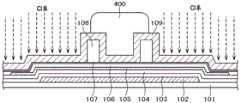
在TFT基板100的一边形成有端子区域20。在端子区域20中,为了向有机EL显示装置供给电源、信号而连接有柔性布线基板600。若由例如0.2mm以下的玻璃形成TFT基板100,则能够将显示器弯曲使用。另外,若由聚酰亚胺等树脂形成TFT基板100,则能够形成柔性的显示装置。聚酰亚胺从机械强度、耐热性等角度作为显示装置的基板具有优异的特性。A
图2为作为对比例的有机EL显示装置的显示区域10的剖视图。在TFT基板100之上形成有基底膜101。基底膜101防止在上层形成的氧化物半导体105被来自玻璃或树脂的杂质污染,并提高在显示装置上形成的膜与树脂基板或玻璃基板的粘接力。FIG. 2 is a cross-sectional view of a
基底膜101例如成为氧化硅膜(以下以SiO表示)、氮化硅膜(以下以SiN表示)、SiO的三层构成。下层的SiO防止杂质侵入并确保与作为TFT基板的玻璃或聚酰亚胺的粘接性。SiN针对来自玻璃基板或聚酰亚胺基板的特别是水分等具有优异的阻隔性。上层的SiO具有针对杂质的阻隔的作用,并提高在SiO之上形成的层与基板的粘接力。The
在图2中,在基底膜101之上形成有底栅电极102。栅电极也形成在氧化物半导体105的上侧,图2的TFT成为所谓的双栅极方式。但是,在图2的构成中,顶栅电极109的影响大于底栅电极102的影响。底栅电极102还具有避免半导体层105受到来自背侧的光的影响的效果。In FIG. 2 , the
在底栅电极102与氧化物半导体105之间形成有由双层构造形成的底栅极绝缘膜。底栅极绝缘膜成为第1底栅极绝缘膜103和第2底栅极绝缘膜104的双层构造。第1底栅极绝缘膜103例如由50nm的氮化硅膜(SiN)形成,第2底栅极绝缘膜104例如由200nm的氧化硅膜(SiO)形成。A bottom gate insulating film formed of a double-layer structure is formed between the
在第2底栅极绝缘膜104之上形成有氧化物半导体105。在氧化物半导体105的与沟道部相当的部分形成有顶栅极绝缘膜106,并在其上形成有顶栅电极109。图2中的TFT的构成使用图3说明。An
在图2中,以覆盖TFT的方式形成有层间绝缘膜110。层间绝缘膜110成为SiN膜、SiO膜或SiN与SiO的层叠构造。图2的层间绝缘膜110具有向氧化物半导体105供给氢的作用。因此,层间绝缘膜110为含有氢的膜较好。In FIG. 2, the
在层间绝缘膜110上形成有贯通孔,以将氧化物半导体105的漏极区域与漏电极111连接、将氧化物半导体105的源极区域与源电极112连接。由丙烯酸等树脂以覆盖层间绝缘膜110、漏电极111、源电极112等的方式形成有机平坦化膜113。有机平坦化膜113具有作为平坦化膜的作用,因此形成得较厚,为1.5μm至4μm左右。Through holes are formed in the
在有机平坦化膜113上形成有贯通孔,以进行下部电极114与源电极112的连接。下部电极114为下层由银的薄膜等形成的反射电极,上侧作为针对有机EL层的阳极动作。阳极由例如作为透明导电膜的ITO(Indium Tin Oxide:氧化铟锌)形成。Through holes are formed in the
以覆盖下部电极114的端部、有机平坦化膜113等的方式形成隔堤115。隔堤115由丙烯酸等树脂形成。隔堤115的作用为避免在下部电极114之上形成的有机EL层116在下部电极114的端部处发生台阶式切断以及对像素间进行划分。隔堤115为初始形成在整个面上,之后在形成有有机EL层116的部分即在发光部分形成孔的构成。The
在图2中,在隔堤115的孔内,在下部电极114之上形成有有机EL层116。有机EL层116例如自下而上依次由空穴注入层、空穴传输层、发光层、电子传输层、电子注入层这5层形成。In FIG. 2 , an
在有机EL层116之上,由透明电极形成有作为阴极的上部电极117。上部电极117必须是透明的。上部电极117例如由ITO、IZO(Indium Zinc Oxide:氧化铟锌)、AZO(AntimonyZinc Oxide:氧化锑锌)等透明导电膜或银等金属的薄膜形成。金属在薄膜化时也接近透明。上部电极117在各像素中公共地形成在显示区域10的整个面上。On the
有机EL层116不耐受水,且因为薄而机械强度低。因此,使用由SiN、SiO、丙烯酸等形成的有机膜等层叠膜形成的保护膜118以覆盖上部电极117的方式形成。SiN成为针对水分的阻隔层,有机膜构成机械缓冲层,SiO发挥作为阻隔层的作用并提高与其他膜的粘接力。The
有机EL显示装置具有反射膜而反射外部光。外部光的反射导致视觉辨认性恶化。由此,图2所示的有机EL显示装置在显示面上借助粘合材料119配置有圆偏振片120以防止外部光的反射。The organic EL display device has a reflective film to reflect external light. The reflection of external light causes deterioration of visibility. Thus, the organic EL display device shown in FIG. 2 is provided with the
图3是图2中的TFT部分的放大剖视图。在图3中,在基底膜101之上使用金属形成有底栅电极102。第1底栅极绝缘膜103由SiN以覆盖底栅电极102的方式形成厚度为例如50nm。在其上由SiO形成有厚度200nm的第2底栅极绝缘膜104。第1底栅极绝缘膜103、第2底栅极绝缘膜104能够连续地通过CVD(Chemical Vapor Deposition:化学气相沉积)形成。FIG. 3 is an enlarged cross-sectional view of a TFT portion in FIG. 2 . In FIG. 3 , the
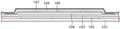
在第2底栅极绝缘膜104之上形成有氧化物半导体105。氧化物半导体105若被氢还原则特性变化。为了使SiN释放氢,与氧化物半导体105接触的第2底栅极绝缘膜104由SiO形成。氧化物半导体105通过例如溅射法形成为10nm至100nm的厚度。氧化物半导体105由例如IGZO形成。An
在图3中,在氧化物半导体105之上,在与氧化物半导体105的沟道对应的部分由SiO形成例如厚度100nm的顶栅极绝缘膜106。顶栅极绝缘膜106例如在整个面上形成SiO之后通过光刻而仅保留在与沟道对应的部分。In FIG. 3 , over the
之后在顶栅极绝缘膜106之上形成顶栅电极109。顶栅电极109的厚度为例如200nm。顶栅极绝缘膜106的厚度为100nm,底栅极绝缘膜为由SiO形成的200nm的第2底栅极绝缘膜104和由SiN形成的50nm的第1栅极绝缘膜103的层叠膜,因此在TFT的Vg-Id特性中,顶栅电极109的影响占主导。以下也存在将顶栅电极109简称为栅电极,将顶栅极绝缘膜106简称为栅极绝缘膜的情况。The
之后,以覆盖栅电极109、氧化物半导体105的方式形成层间绝缘膜110。在许多情况下,层间绝缘膜110设为下层为SiN膜、上层为SiO膜的层叠构造。之所以将下层设为SiN膜,是为了从SiN膜向氧化物半导体105供给氢以在氧化物半导体105上形成漏极区域和源极区域。即,在退火工序中,氢扩散至氧化物半导体105的未被栅电极109覆盖部分,对氧化物半导体105赋予导电性。由此,在氧化物半导体105上形成漏极区域及源极区域。并且,在层间绝缘膜110上形成贯通孔,将氧化物半导体105的漏极与漏电极111连接,将氧化物半导体105的源极与源电极112连接。After that, the
另一方面,氢未向氧化物半导体105中由栅电极109覆盖的部分扩散,因此保持高电阻。但是,被氧化物半导体105的漏极及源极吸收的来自SiN的氢在退火工序中也沿氧化物半导体105的横向扩散。由此,在沟道长度短的情况下会出现沟道导通的问题。或者虽然沟道未导通,但出现Vd-Id特性出现偏差的问题。On the other hand, hydrogen is not diffused to the portion covered by the
本发明能够应对上述问题。图4是本发明的有机EL显示装置的显示区域10的剖视图。图4与图2的区别在于具有氧化物半导体105的TFT的构成及覆盖TFT的层间绝缘膜110的构成。在图4中,由SiO形成第2底栅极绝缘膜104、在其上形成氧化物半导体105并进行图案化,至此与图2相同。The present invention can cope with the above-mentioned problems. FIG. 4 is a cross-sectional view of the
在图4中,在与氧化物半导体105的由漏极区域和源极区域夹入的区域对应的部分形成有由SiO形成的栅极绝缘膜106,在其上形成有氧化铝膜(以下记为AlO)107。虽然也可以由SiO膜106和AlO膜107形成栅极绝缘膜,但在本说明书中,方便起见将SiO膜称为栅极绝缘膜106,将氧化铝膜称为AlO膜107。In FIG. 4, a
在AlO膜107之上由金属或合金形成有栅电极109,而本发明的特征为在AlO膜107的两端形成有由例如SiN等绝缘膜形成的侧壁间隔件108。如后所述,能够通过该侧壁间隔件108可靠地将沟道与漏极或源极分离开。A
栅电极109及栅极绝缘膜106被图案化,氧化物半导体105的漏极及源极未由栅极绝缘膜106或栅电极109覆盖而与层间绝缘膜110直接接触。层间绝缘膜110成为SiN膜或SiN膜与SiO膜的双层构造。本发明的特征之一为SiN膜直接与氧化物半导体105的漏极或源极接触。因此能够向漏极及源极供给氢,减小漏极及源极的电阻。The
在向漏极及源极供给了氢的情况下,由于氢容易扩散,因此在作为对比例的图3的构成中,在退火工序中氢扩散,TFT的特性变得不稳定。此外,若沟道长度变短,则还会出现沟道导通的危险。本发明特别是通过在栅电极109的两侧形成侧壁间隔件108来防止具有氧化物半导体的TFT的特性变得不稳定。层间绝缘膜110之上的构成与使用图2说明的内容相同。When hydrogen is supplied to the drain and the source, since hydrogen is easily diffused, in the configuration of FIG. 3 as a comparative example, hydrogen diffuses during the annealing step, and the characteristics of the TFT become unstable. In addition, if the channel length is shortened, there is also a risk of channel conduction. In particular, the present invention prevents the characteristics of the TFT having an oxide semiconductor from becoming unstable by forming
图5为图4中的TFT周边的剖视图。在图5中,在氧化物半导体105之上形成有栅极绝缘膜106、AlO膜107及栅电极109。在栅电极109的端部与AlO膜107之间形成有侧壁间隔件108。栅电极109的未夹持侧壁间隔件108而与氧化物半导体105相对的部分成为氧化物半导体105的沟道1051。换言之,图5中的氧化物半导体105的与形成栅电极109的金属中成为凹部1091的部分对应的部分成为沟道1051。FIG. 5 is a cross-sectional view of the periphery of the TFT in FIG. 4 . In FIG. 5 , a
栅极绝缘膜106仅形成在栅电极109的下侧,氧化物半导体105的成为漏极、源极的部分未被覆盖。之后由SiN以覆盖栅电极109、氧化物半导体105等的方式形成层间绝缘膜110。由于氧化物半导体105的与SiN膜接触的部分被供给氢,因此漏极及源极成为低电阻,能够增大漏极电流。The
以往,使缺陷相对较多的SiO与氧化物半导体105接触而形成漏极及源极,但就氢的释放而言比SiN少,因此无法充分地使漏极及源极低电阻化,无法增大漏极电流。另一方面,在现有的构成中由SiN形成层间绝缘膜110时,氢被向氧化物半导体105供给,但该氢也向氧化物半导体105的沟道1051扩散而使沟道导通。特别是,在沟道长度短的TFT中,该危险很大。Conventionally, the drain and source electrodes are formed by contacting SiO, which has relatively many defects, with the
本发明通过在栅电极109的两旁形成侧壁间隔件108来控制的氢向沟道1051扩散,同时实现氧化物半导体105中的漏极及源极的低电阻化和防止氢对沟道1051的影响。本发明还在栅极绝缘膜106与栅电极109及侧壁间隔件108之间形成AlO膜107,从而进一步增强该效果。The present invention controls the diffusion of hydrogen into the
在图5中,位于栅极绝缘膜106与栅电极109及侧壁间隔件108之间的AlO膜107的厚度为10至50nm。为了抑制氧化物半导体105的沟道的特性变化,供给氧是有效的。因此,通过还从AlO膜107供给氧而更加稳定地向氧化物半导体105供给氧。In FIG. 5 , the thickness of the
在AlO膜107之上形成的侧壁间隔件108的形状在截面中为一个侧壁形成倾斜的梯形。通过侧壁间隔件108而在氧化物半导体105上形成偏移区域(offset region)1052。偏移区域1052可靠地形成氧化物半导体105的沟道与漏极及源极(以下以漏极表示)之间的中间区域,即使在向漏极或源极供给了大量氢的情况下,也能够防止该氢对沟道造成影响,防止TFT的特性不均匀。特别是在沟道长度变短的情况下,该效果显著。The shape of the
在图5中,偏移区域1052的长度d2为0.5μm至2μm。例如,在沟道长度d1为2μm的情况下,优选偏移区域1052的长度d2为1μm左右。在偏移区域1051与侧壁间隔件108之间存在AlO膜107。该AlO膜107成为氧的良好的供给源,因此使欲从漏极向沟道侧扩散的氢偏移,有效防止沟道1051被氢还原。In FIG. 5 , the length d2 of the offset
在图5中,栅电极109搭在侧壁间隔件108的上表面上。这是为了稳定地形成栅电极109。栅电极109搭在侧壁间隔件108上的量d3优选0.1μm以上。在俯视观察时,从栅电极109的端部到偏移区域1052的端部的距离为d4。d4优选0.3μm以上。偏移区域1052的宽度d2成为d3+d4。In FIG. 5 , the
在图5中,侧壁间隔件108的一个侧壁成为倾斜面。将侧壁间隔件108的侧壁设为倾斜面的理由为,提高以覆盖栅电极109、侧壁间隔件108的方式形成的层间绝缘膜110的阶梯覆盖率。因此,倾斜面并非本发明的必要构成要素。In FIG. 5 , one side wall of the
侧壁间隔件108的厚度例如为100nm至500nm。若侧壁间隔件108的厚度过小,则在通过干蚀刻对侧壁间隔件进行加工时,其会消失。另一方面,在侧壁间隔件108的厚度过大的情况下,会出现覆盖栅电极109、侧壁间隔件108的层间绝缘膜110的台阶式切断的问题、侧壁间隔件108的加工时间变长等问题。另外,若侧壁间隔件108的厚度过大,则在侧壁间隔件108由SiN形成的情况下,会出现来自侧壁间隔件108自身的氢的供给量增多的问题。The thickness of the
以覆盖栅电极109及侧壁间隔件108的方式形成有层间绝缘膜110。层间绝缘膜110通常由SiN和SiO这两层膜形成,但若可以,则较好的是与氧化物半导体105接触的下层由SiN膜形成。SiN膜成为氢的供给体,能够减小氧化物半导体105的漏极区域和源电极区域的电阻。An interlayer insulating
在图5中,如后所述,侧壁间隔件108的材质根据干蚀刻的微细加工的要求而优选由SiN形成,但根据加工条件,也可以由SiON(氮氧化硅)或SiO形成。在由SiN形成侧壁间隔件108的情况下,构成层间绝缘膜110的SiN与构成侧壁间隔件108的SiN也可以是相同的膜质。但是,优选构成层间绝缘膜110的SiN的氢含量比构成侧壁间隔件108的SiN的氢含量多。也就是说,由于侧壁间隔件108接近沟道,因此较好是抑制来自侧壁间隔件108的氢的供给。In FIG. 5 , as described later, the material of the
各种SiN均通过CVD形成,而即使是相同的气体比、功率、成膜压力等,也是只要将成膜侧壁间隔件108时的成膜温度设定为高温(例如300℃至350℃)即可。高温成膜的情况下,由于膜的均镀性更好,因此还具有不易形成气坑的优点。Various SiNs are formed by CVD, and even if the gas ratio, power, film-forming pressure, etc. are the same, the film-forming temperature at the time of film-forming the
图6是TFT的俯视图。在图6中,在底栅电极102之上隔着底栅极绝缘膜形成有氧化物半导体105。在氧化物半导体105之上以岛状形成有栅极绝缘膜,但在图6中被栅电极109及侧壁间隔件108覆盖而不可见。在图6中,能够在栅电极109的周围看到侧壁间隔件108,其为图5中的侧壁间隔件108的倾斜面。FIG. 6 is a plan view of a TFT. In FIG. 6 , an
在栅电极109上形成有凹部1091。在栅电极109的形成有凹部1091的部分形成有氧化物半导体105的沟道,在凹部1091的两侧形成有偏移区域1052。在图6中,构成层间绝缘膜110的SiN与未与栅电极109、侧壁间隔件108重叠的氧化物半导体105接触,氧化物半导体105被从SiN供给的氢还原,形成漏极及源极。在漏极经由贯通孔连接漏电极111,在源极经由贯通孔连接源电极112。A
图7至图12是示出实现图5的构成的制造工序的剖视图。在图7中,在基底膜101之上形成有底栅电极102,并以覆盖该底栅电极102的方式形成有第1底栅极绝缘膜103、第2底栅极绝缘膜104,在其上形成有氧化物半导体105。底栅电极102在使用溅射法成膜后进行图案化。第1底栅极绝缘膜103由SiN以例如厚度50nm形成,第2底栅极绝缘膜104由SiO以例如厚度200nm形成。SiN与SiO能够连续地通过CVD形成。7 to 12 are cross-sectional views showing manufacturing steps for realizing the configuration of FIG. 5 . In FIG. 7 , a
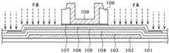
之后在第2底栅极绝缘膜104之上形成氧化物半导体105。氧化物半导体105在以10至100nm成膜后图案化为岛状。之后由SiO在氧化物半导体105之上形成顶栅极绝缘膜(栅极绝缘膜)106。SiO的膜厚例如为100nm。底栅极绝缘膜与顶栅极绝缘膜的膜厚的关系如使用图2所说明。之后通过溅射法形成10至50nm的厚度的AlO膜107。Then, the
图8是示出用于形成侧壁间隔件108的中间工序的剖视图。在图8中,通过CVD以100nm至500nm的厚度成膜用于形成侧壁间隔件108的SiN膜。形成该SiN的CVD与形成之后形成的层间绝缘膜110的CVD相比在高温(例如300℃至350℃)下进行。采用更致密的膜质以抑制氢的释放。在图8中,在SiN膜之上形成用于使侧壁间隔件图案化的抗蚀剂400。之后,使用SF6系的气体对SiN膜进行干蚀刻。FIG. 8 is a cross-sectional view illustrating an intermediate process for forming the
图9是示出对侧壁间隔件108用的SiN膜进行干蚀刻后的状态的剖视图。SiN易于通过使用SF6系的气体的干蚀刻而被侧蚀刻。以图9的箭头示出侧蚀刻的情形。通过侧蚀刻,侧壁间隔件108的宽度变得小于抗蚀剂的宽度。侧壁间隔件的宽度在底面处非常小,为0.5μm至2μm,因此难以形成这样的抗蚀剂图案。通过使用SiN,根据侧蚀刻的效果,能够将侧壁间隔件108加工为抗蚀剂的图案化极限以下的尺寸。FIG. 9 is a cross-sectional view showing a state in which the SiN film for the
将AlO与构成侧壁间隔件的SiN进行对比可知,在使用SF6系气体的干蚀刻中,AlO的选择比与SiN相比非常大,因此在图9所示的干蚀刻工序中,AlO膜基本未被蚀刻。Comparing AlO with SiN constituting the sidewall spacers, it can be seen that in dry etching using SF6-based gas, the selectivity ratio of AlO is very large compared to SiN, so in the dry etching process shown in FIG. 9, the AlO film is basically Not etched.
之后如图10所示,对成为栅电极109的金属或合金进行成膜,在希望作为栅电极109保留的部分形成抗蚀剂400。作为栅电极109,例如使用Mo、MoW或Ti-Al-Ti等层叠膜。并且,通过使用Cl系气体的干蚀刻对金属及AlO膜进行蚀刻,使AlO膜107及栅电极109图案化。在使用Cl系气体的情况下,构成栅极绝缘膜106的SiO虽难以被蚀刻,但由于不是零,因此根据需要在SiO的蚀刻中途使Cl系的干蚀刻停止。After that, as shown in FIG. 10 , the metal or alloy to be the
图11是示出通过图10所示的使用Cl系气体的干蚀刻而使栅电极109及AlO膜107图案化后的状态的剖视图。在该状态下,氧化物半导体105由栅极绝缘膜106覆盖。由此,如图11所示,通过F系的干蚀刻对成为栅极绝缘膜的材料的SiO进行蚀刻,使栅极绝缘膜106图案化。在F系的干蚀刻中,氧化物半导体105几乎未被蚀刻。FIG. 11 is a cross-sectional view showing a state in which the
图12是示出通过F系的干蚀刻将SiO去除以使栅极绝缘膜106图案化后的状态的剖视图。构成侧壁间隔件108的SiN也通过F系的干蚀刻被蚀刻若干,因此在侧壁间隔件108的外侧的壁上形成锥形状。12 is a cross-sectional view showing a state in which SiO is removed by F-based dry etching to pattern the
在图12中,栅电极109残留在截面为梯形状的侧壁间隔件108的上底。该量为d3。d3优选0.1μm以上。优选侧壁间隔件108的下底与侧壁间隔件108的上底的差为0.3μm以上。In FIG. 12 , the
之后针对图12的构成形成层间绝缘膜110,则成为图5的构成。层间绝缘膜110由SiN或SiN和SiO的层叠膜形成,而由于层间绝缘膜110会向氧化物半导体105供给氢,因此在采用层叠膜的情况下,最好是与氧化物半导体105接触的层由SiN形成。另外,优选层间绝缘膜110中的SiN的氢的含量比构成侧壁间隔件108的SiN多。After that, the
实施例2Example 2
图13是表示本发明的实施例2的有机EL显示装置的显示区域的剖视图。在图13中,顶栅极绝缘膜106并非仅形成在栅电极109的下方而是形成在整个面上。另外,侧壁间隔件108的侧面不倾斜。图13的其他构成与图4相同。在图13中,氧化物半导体105的漏极区域及源极区域与层间绝缘膜110不接触。因此,即使由SiN形成层间绝缘膜110,也无法从SiN接受氢。因此,为了形成氧化物半导体105的漏极区域及源极区域,如图14所示,需要另行进行离子注入(I/I)。13 is a cross-sectional view showing a display region of an organic EL display device according to Example 2 of the present invention. In FIG. 13 , the top
图14的剖面构造与实施例1的图11相同。但在图14中,不进行干蚀刻而是进行离子注入(I/I),在氧化物半导体105中掺杂硼(B)或磷(P)等而赋予导电性,在氧化物半导体上形成漏极及源极。需要说明的是,离子注入(I/I)是使氧化物半导体105的构造产生缺陷以赋予导电性,因此也可以注入Ar等。离子注入(I/I)以栅电极109为掩膜来进行。另外,侧壁间隔件108也形成得较厚,而且在该部分也存在AlO膜107,因此在沟道与漏极及源极之间构成中间区域。需要说明的是,在离子注入(I/I)中,侧壁间隔件108未被蚀刻,因此侧壁间隔件108的侧面不易形成图12所示的倾斜。The cross-sectional structure of FIG. 14 is the same as that of FIG. 11 of the first embodiment. However, in FIG. 14 , ion implantation (I/I) is performed instead of dry etching, and the
图15是示出在离子注入后形成层间绝缘膜110并在该层间绝缘膜110上形成贯通孔,连接有漏电极111和源电极112的状态的剖视图。层间绝缘膜110的构成与使用实施例1的图5等说明的内容相同。在实施例2中,氧化物半导体105的漏极区域及源极区域通过离子注入而被赋予导电性。15 is a cross-sectional view showing a state in which the
氧化物半导体105的漏极区域及源极区域由含有大量氧的栅极绝缘膜106覆盖。由此,即使通过离子注入赋予导电性,漏极区域、源极区域也由于氧的影响而存在电阻逐渐上升的可能性。The drain region and the source region of the
通过由SiN构成层间绝缘膜110的与栅极绝缘膜106接触的面,从而通过来自SiN的氢的供给来缓和由来自栅极绝缘膜106的氧对氧化物半导体105的漏极及源极的影响。因此能够使TFT的特性稳定化。其他构成与实施例1中说明的内容相同。By forming the surface of the
实施例3Example 3
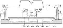
在实施例1及2中说明了将本发明应用于有机EL显示装置的情况。但本发明也能够应用于液晶显示装置。图16是液晶显示装置的俯视图。在图16中,TFT基板100与对置基板200通过密封材料30粘接,在密封材料30的内侧,在TFT基板100与对置基板200之间夹持有液晶。In
在TFT基板100与对置基板200重叠的部分形成有显示区域10。在显示区域10中,扫描线91沿横向(x方向)延伸并沿纵向(y方向)排列。另外,影像信号线92沿纵向延伸并沿横向排列。在由扫描线91和影像信号线92包围的区域中形成有像素95。TFT基板100形成得比对置基板200大,TFT基板100的未与对置基板200重叠的部分成为端子区域20。在端子区域20中连接用于向液晶显示装置供给电源、信号的柔性布线基板600。The
图17是液晶显示装置的显示区域的剖视图。在图17中,直到有机平坦化膜110的形成为止与实施例1的图4相同。需要说明的是,实施例1的图4的TFT为驱动有机EL层的驱动TFT,而本实施例的TFT为开关TFT,但基本构成相同。17 is a cross-sectional view of a display region of a liquid crystal display device. In FIG. 17 , up to the formation of the
即,在兼作为遮光膜的第1栅电极102之上形成有双层构成的底栅极绝缘膜(103、104),在其上形成有氧化物半导体105。在氧化物半导体105中的与沟道对应的部分形成顶栅极绝缘膜106。在顶栅极绝缘膜106之上形成AlO膜107。并且,在AlO膜107的上部两端形成作为本发明的特征的侧壁间隔件108。之后形成栅电极109。That is, a bottom gate insulating film (103, 104) having a double-layer structure is formed on the
以覆盖栅电极109、侧壁间隔件108、氧化物半导体105等的方式形成层间绝缘膜110。层间绝缘膜110的构成也与使用图5说明的内容相同。并且,在层间绝缘膜110上形成贯通孔,以使氧化物半导体105的漏极与漏电极111连接、使氧化物半导体105的源极与源电极112连接。以覆盖漏电极111、源电极112、层间绝缘膜110的方式形成有机平坦化膜113。The
在图17中,在有机平坦化膜113之后形成的构成与图4所示的有机EL显示装置不同。图17是IPS(In Plane Switching:共面转换)方式的液晶显示装置的剖视图。在图17中,在有机平坦化膜113上形成用于连接源电极112与像素电极152的贯通孔。在图17中,在有机平坦化膜113之上形成有由ITO形成的公共电极150。由SiN以覆盖公共电极150的方式形成电容绝缘膜151。In FIG. 17 , the configuration formed after the
在电容绝缘膜151之上形成有像素电极152。像素电极152在有机平坦化膜113上形成的贯通孔中与源电极112连接。需要说明的是,电容绝缘膜151覆盖有机平坦化膜113的贯通孔的侧壁,但在下部形成贯通孔,以使得像素电极152能够与源电极112连接。在像素电极152之上形成有用于使液晶初始取向的取向膜153。A
夹着液晶层300而以与TFT基板100相对的方式形成有对置基板200。在对置基板200的内侧形成有黑矩阵202,在与像素电极122对应的部分形成有彩色滤光片201。以覆盖黑矩阵202及彩色滤光片201的方式形成有顶涂膜203。为了使液晶初始取向而在顶涂膜203之上形成有取向膜204。The opposing
在图17中,在向像素电极122施加影像信号时产生如箭头所示的电力线,使液晶分子301旋转,控制像素中的来自背光源的光的透射率,以形成图像。In FIG. 17, when the image signal is applied to the pixel electrode 122, electric force lines as indicated by arrows are generated, the
如上所述,在液晶显示装置中也能够通过应用实施例1的构成的TFT来形成特性稳定的使用氧化物半导体的TFT。在实施例2中说明的构成也同样地能够应用于液晶显示装置。As described above, a TFT using an oxide semiconductor having stable characteristics can be formed by applying the TFT having the configuration of Example 1 to a liquid crystal display device. The configuration described in Embodiment 2 can be similarly applied to a liquid crystal display device.
在以上的说明中,说明了IPS方式的液晶显示装置,但也能够应用于其他方式的液晶显示装置。In the above description, the liquid crystal display device of the IPS system has been described, but it can also be applied to liquid crystal display devices of other systems.
氧化物半导体能够减小漏电流,但由于迁移率小于多晶硅,因此存在难以由使用氧化物半导体的TFT构成周边驱动电路例如图1中的扫描线驱动电路80的情况。在这一点上,多晶硅由于迁移率大,因此能够将使用多晶硅的TFT应用于周边驱动电路。Oxide semiconductors can reduce leakage current, but since the mobility is lower than that of polysilicon, it may be difficult to configure peripheral driver circuits such as the scan
另一方面,使用多晶硅的TFT的漏电流较大,因此像素电极的电位变化成为问题。因此,显示区域中的像素应用使用氧化物半导体的TFT,而周边驱动电路中应用使用多晶硅的TFT是合理的。将这样的构成称为混合式,本发明也能够应用于这样的混合式的显示装置。On the other hand, since the leakage current of the TFT using polysilicon is large, the potential change of the pixel electrode becomes a problem. Therefore, it is reasonable to use TFTs using oxide semiconductors for pixels in the display area, and TFTs using polysilicon for peripheral driving circuits. Such a configuration is called a hybrid type, and the present invention can also be applied to such a hybrid type display device.
附图标记说明Description of reference numerals
10…显示区域、20…端子区域、30…密封材料、80…扫描线驱动电路、91…扫描线、92…影像信号线、93…电源线、95…像素、100…TFT基板、101…基底膜、102…底栅电极、103…第1底栅极绝缘膜、104…第2底栅极绝缘膜、105…氧化物半导体、106…栅极绝缘膜、107…AlO膜、108…侧壁间隔件、109…栅电极、110…层间绝缘膜、111…漏电极、112…源电极、113…有机平坦化膜、114…下部电极、115…隔堤、116…有机EL层、117…上部电极、118…保护膜、119…粘合材料、120…圆偏振片、150…公共电极、151…电容绝缘膜、152…像素电极、153…取向膜、200…对置基板、201…彩色滤光片、202…黑矩阵、203…顶涂膜、204…取向膜、300…液晶层、400…抗蚀剂、301…液晶分子、1051…沟道、1052…偏移区域、1091…栅电极的凹部、I/I…离子注入10...display area, 20...terminal area, 30...sealing material, 80...scanning line driver circuit, 91...scanning line, 92...image signal line, 93...power supply line, 95...pixel, 100...TFT substrate, 101...substrate film, 102...bottom gate electrode, 103...first bottom gate insulating film, 104...second bottom gate insulating film, 105...oxide semiconductor, 106...gate insulating film, 107...AlO film, 108...sidewall Spacer, 109...gate electrode, 110...interlayer insulating film, 111...drain electrode, 112...source electrode, 113...organic planarizing film, 114...lower electrode, 115...bank, 116...organic EL layer, 117... Upper electrode, 118...protective film, 119...adhesive material, 120...circular polarizer, 150...common electrode, 151...capacitive insulating film, 152...pixel electrode, 153...alignment film, 200...counter substrate, 201...color Filter, 202...Black matrix, 203...Top coating film, 204...Orientation film, 300...Liquid crystal layer, 400...Resist, 301...Liquid crystal molecules, 1051...Channel, 1052...Offset region, 1091...Gate Electrode recess, I/I...Ion implantation
Claims (20)
Translated fromChinesePriority Applications (1)
| Application Number | Priority Date | Filing Date | Title |
|---|---|---|---|
| CN202210280593.6ACN114649259B (en) | 2018-01-11 | 2018-11-28 | Method for manufacturing a display device |
Applications Claiming Priority (3)
| Application Number | Priority Date | Filing Date | Title |
|---|---|---|---|
| JP2018-002641 | 2018-01-11 | ||
| JP2018002641AJP7022592B2 (en) | 2018-01-11 | 2018-01-11 | Display device |
| PCT/JP2018/043661WO2019138714A1 (en) | 2018-01-11 | 2018-11-28 | Display device |
Related Child Applications (1)
| Application Number | Title | Priority Date | Filing Date |
|---|---|---|---|
| CN202210280593.6ADivisionCN114649259B (en) | 2018-01-11 | 2018-11-28 | Method for manufacturing a display device |
Publications (2)
| Publication Number | Publication Date |
|---|---|
| CN111512356Atrue CN111512356A (en) | 2020-08-07 |
| CN111512356B CN111512356B (en) | 2022-04-08 |
Family
ID=67218253
Family Applications (2)
| Application Number | Title | Priority Date | Filing Date |
|---|---|---|---|
| CN202210280593.6AActiveCN114649259B (en) | 2018-01-11 | 2018-11-28 | Method for manufacturing a display device |
| CN201880083528.6AActiveCN111512356B (en) | 2018-01-11 | 2018-11-28 | Display device |
Family Applications Before (1)
| Application Number | Title | Priority Date | Filing Date |
|---|---|---|---|
| CN202210280593.6AActiveCN114649259B (en) | 2018-01-11 | 2018-11-28 | Method for manufacturing a display device |
Country Status (4)
| Country | Link |
|---|---|
| US (4) | US11309336B2 (en) |
| JP (1) | JP7022592B2 (en) |
| CN (2) | CN114649259B (en) |
| WO (1) | WO2019138714A1 (en) |
Cited By (1)
| Publication number | Priority date | Publication date | Assignee | Title |
|---|---|---|---|---|
| CN114639687A (en)* | 2020-12-15 | 2022-06-17 | 夏普株式会社 | Active Matrix Substrate |
Families Citing this family (5)
| Publication number | Priority date | Publication date | Assignee | Title |
|---|---|---|---|---|
| US11009757B2 (en)* | 2019-03-14 | 2021-05-18 | Sharp Kabushiki Kaisha | Liquid crystal display |
| WO2021144666A1 (en)* | 2020-01-16 | 2021-07-22 | 株式会社半導体エネルギー研究所 | Semiconductor device and method for manufacturing semiconductor device |
| KR102850343B1 (en)* | 2021-02-03 | 2025-08-28 | 삼성디스플레이 주식회사 | Transistor and display device including the same |
| WO2023062695A1 (en)* | 2021-10-11 | 2023-04-20 | シャープディスプレイテクノロジー株式会社 | Display device |
| EP4618157A1 (en)* | 2024-03-11 | 2025-09-17 | Huawei Technologies Co., Ltd. | Transistor device and method |
Citations (23)
| Publication number | Priority date | Publication date | Assignee | Title |
|---|---|---|---|---|
| US20070072439A1 (en)* | 2005-09-29 | 2007-03-29 | Semiconductor Energy Laboratory Co., Ltd. | Semiconductor device and manufacturing method thereof |
| CN101093854A (en)* | 2006-06-21 | 2007-12-26 | 株式会社东芝 | Semiconductor device and method of manufacturing the same |
| JP2009111302A (en)* | 2007-11-01 | 2009-05-21 | Hitachi Ltd | Semiconductor device and manufacturing method thereof |
| US20110012106A1 (en)* | 2009-07-17 | 2011-01-20 | Semiconductor Energy Laboratory Co., Ltd. | Semiconductor device and manufacturing method thereof |
| CN102822981A (en)* | 2010-04-07 | 2012-12-12 | 夏普株式会社 | Circuit board, display device, and method for manufacturing circuit board |
| JP2012256871A (en)* | 2011-05-19 | 2012-12-27 | Semiconductor Energy Lab Co Ltd | Semiconductor device manufacturing method |
| JP2013050503A (en)* | 2011-08-30 | 2013-03-14 | Japan Display West Co Ltd | Liquid crystal optical element |
| JP2013123041A (en)* | 2011-11-11 | 2013-06-20 | Semiconductor Energy Lab Co Ltd | Semiconductor device and semiconductor device manufacturing method |
| CN103477441A (en)* | 2011-04-18 | 2013-12-25 | 夏普株式会社 | Thin-film transistor, display panel, and method for producing thin-film transistor |
| CN103515395A (en)* | 2012-06-14 | 2014-01-15 | 株式会社日本显示器 | Display device and manufacturing method for same |
| JP2014131047A (en)* | 2012-12-31 | 2014-07-10 | Samsung Display Co Ltd | Thin-film transistor and thin-film transistor display board |
| CN104078511A (en)* | 2013-03-28 | 2014-10-01 | 索尼公司 | Semiconductor device, display unit, and electronic apparatus |
| KR20160018928A (en)* | 2014-08-07 | 2016-02-18 | 삼성디스플레이 주식회사 | Thin film transistor and method for manufacturing of the same |
| CN105355661A (en)* | 2015-10-10 | 2016-02-24 | 无锡盈芯半导体科技有限公司 | Thin film transistor and preparation method for semiconductor channel layer of thin film transistor |
| US20170053951A1 (en)* | 2015-08-19 | 2017-02-23 | Japan Display Inc. | Display device |
| US20170117374A1 (en)* | 2015-10-27 | 2017-04-27 | Nlt Technologies, Ltd. | Thin film transistor, display device, and method for manufacturing thin film transistor |
| CN106981520A (en)* | 2017-04-12 | 2017-07-25 | 京东方科技集团股份有限公司 | Thin film transistor (TFT) and preparation method thereof, array base palte and display device |
| CN107017287A (en)* | 2015-10-27 | 2017-08-04 | Nlt科技股份有限公司 | The manufacture method of thin film transistor (TFT), display device and thin film transistor (TFT) |
| JP2017152701A (en)* | 2011-05-13 | 2017-08-31 | 株式会社半導体エネルギー研究所 | Semiconductor device |
| CN107210013A (en)* | 2015-01-21 | 2017-09-26 | 株式会社日本显示器 | Display device |
| CN107275397A (en)* | 2016-03-30 | 2017-10-20 | 瑞萨电子株式会社 | The manufacture method of semiconductor devices and semiconductor devices |
| JP2017204659A (en)* | 2012-01-20 | 2017-11-16 | 株式会社半導体エネルギー研究所 | Semiconductor device |
| CN107408578A (en)* | 2015-03-30 | 2017-11-28 | 堺显示器制品株式会社 | Thin film transistor and display panel |
Family Cites Families (13)
| Publication number | Priority date | Publication date | Assignee | Title |
|---|---|---|---|---|
| KR100229678B1 (en)* | 1996-12-06 | 1999-11-15 | 구자홍 | Thin film transistor and its manufacturing method |
| JPH1197705A (en)* | 1997-09-23 | 1999-04-09 | Semiconductor Energy Lab Co Ltd | Semiconductor integrated circuit |
| US20120242923A1 (en)* | 2010-02-25 | 2012-09-27 | Sharp Kabushiki Kaisha | Thin film transistor substrate, method for manufacturing the same, and display device |
| US9960278B2 (en)* | 2011-04-06 | 2018-05-01 | Yuhei Sato | Manufacturing method of semiconductor device |
| US9287405B2 (en)* | 2011-10-13 | 2016-03-15 | Semiconductor Energy Laboratory Co., Ltd. | Semiconductor device comprising oxide semiconductor |
| US8748240B2 (en)* | 2011-12-22 | 2014-06-10 | Semiconductor Energy Laboratory Co., Ltd. | Method for manufacturing semiconductor device |
| US9653614B2 (en)* | 2012-01-23 | 2017-05-16 | Semiconductor Energy Laboratory Co., Ltd. | Semiconductor device and method for manufacturing the same |
| US8981370B2 (en)* | 2012-03-08 | 2015-03-17 | Semiconductor Energy Laboratory Co., Ltd. | Semiconductor device |
| US9048323B2 (en)* | 2012-04-30 | 2015-06-02 | Semiconductor Energy Laboratory Co., Ltd. | Semiconductor device |
| JP6186166B2 (en)* | 2012-05-02 | 2017-08-23 | 株式会社半導体エネルギー研究所 | Semiconductor device |
| JP6539873B2 (en)* | 2016-03-16 | 2019-07-10 | 株式会社Joled | Thin film transistor, and display device provided with thin film transistor |
| JP2017191834A (en)* | 2016-04-12 | 2017-10-19 | 株式会社Joled | Thin film transistor substrate |
| JP2018190753A (en)* | 2017-04-28 | 2018-11-29 | 株式会社半導体エネルギー研究所 | Semiconductor device and display device |
- 2018
- 2018-01-11JPJP2018002641Apatent/JP7022592B2/enactiveActive
- 2018-11-28CNCN202210280593.6Apatent/CN114649259B/enactiveActive
- 2018-11-28WOPCT/JP2018/043661patent/WO2019138714A1/ennot_activeCeased
- 2018-11-28CNCN201880083528.6Apatent/CN111512356B/enactiveActive
- 2020
- 2020-07-07USUS16/922,438patent/US11309336B2/enactiveActive
- 2022
- 2022-03-15USUS17/694,754patent/US11791346B2/enactiveActive
- 2023
- 2023-09-01USUS18/459,677patent/US12159876B2/enactiveActive
- 2024
- 2024-10-21USUS18/921,200patent/US20250048741A1/enactivePending
Patent Citations (23)
| Publication number | Priority date | Publication date | Assignee | Title |
|---|---|---|---|---|
| US20070072439A1 (en)* | 2005-09-29 | 2007-03-29 | Semiconductor Energy Laboratory Co., Ltd. | Semiconductor device and manufacturing method thereof |
| CN101093854A (en)* | 2006-06-21 | 2007-12-26 | 株式会社东芝 | Semiconductor device and method of manufacturing the same |
| JP2009111302A (en)* | 2007-11-01 | 2009-05-21 | Hitachi Ltd | Semiconductor device and manufacturing method thereof |
| US20110012106A1 (en)* | 2009-07-17 | 2011-01-20 | Semiconductor Energy Laboratory Co., Ltd. | Semiconductor device and manufacturing method thereof |
| CN102822981A (en)* | 2010-04-07 | 2012-12-12 | 夏普株式会社 | Circuit board, display device, and method for manufacturing circuit board |
| CN103477441A (en)* | 2011-04-18 | 2013-12-25 | 夏普株式会社 | Thin-film transistor, display panel, and method for producing thin-film transistor |
| JP2017152701A (en)* | 2011-05-13 | 2017-08-31 | 株式会社半導体エネルギー研究所 | Semiconductor device |
| JP2012256871A (en)* | 2011-05-19 | 2012-12-27 | Semiconductor Energy Lab Co Ltd | Semiconductor device manufacturing method |
| JP2013050503A (en)* | 2011-08-30 | 2013-03-14 | Japan Display West Co Ltd | Liquid crystal optical element |
| JP2013123041A (en)* | 2011-11-11 | 2013-06-20 | Semiconductor Energy Lab Co Ltd | Semiconductor device and semiconductor device manufacturing method |
| JP2017204659A (en)* | 2012-01-20 | 2017-11-16 | 株式会社半導体エネルギー研究所 | Semiconductor device |
| CN103515395A (en)* | 2012-06-14 | 2014-01-15 | 株式会社日本显示器 | Display device and manufacturing method for same |
| JP2014131047A (en)* | 2012-12-31 | 2014-07-10 | Samsung Display Co Ltd | Thin-film transistor and thin-film transistor display board |
| CN104078511A (en)* | 2013-03-28 | 2014-10-01 | 索尼公司 | Semiconductor device, display unit, and electronic apparatus |
| KR20160018928A (en)* | 2014-08-07 | 2016-02-18 | 삼성디스플레이 주식회사 | Thin film transistor and method for manufacturing of the same |
| CN107210013A (en)* | 2015-01-21 | 2017-09-26 | 株式会社日本显示器 | Display device |
| CN107408578A (en)* | 2015-03-30 | 2017-11-28 | 堺显示器制品株式会社 | Thin film transistor and display panel |
| US20170053951A1 (en)* | 2015-08-19 | 2017-02-23 | Japan Display Inc. | Display device |
| CN105355661A (en)* | 2015-10-10 | 2016-02-24 | 无锡盈芯半导体科技有限公司 | Thin film transistor and preparation method for semiconductor channel layer of thin film transistor |
| US20170117374A1 (en)* | 2015-10-27 | 2017-04-27 | Nlt Technologies, Ltd. | Thin film transistor, display device, and method for manufacturing thin film transistor |
| CN107017287A (en)* | 2015-10-27 | 2017-08-04 | Nlt科技股份有限公司 | The manufacture method of thin film transistor (TFT), display device and thin film transistor (TFT) |
| CN107275397A (en)* | 2016-03-30 | 2017-10-20 | 瑞萨电子株式会社 | The manufacture method of semiconductor devices and semiconductor devices |
| CN106981520A (en)* | 2017-04-12 | 2017-07-25 | 京东方科技集团股份有限公司 | Thin film transistor (TFT) and preparation method thereof, array base palte and display device |
Cited By (1)
| Publication number | Priority date | Publication date | Assignee | Title |
|---|---|---|---|---|
| CN114639687A (en)* | 2020-12-15 | 2022-06-17 | 夏普株式会社 | Active Matrix Substrate |
Also Published As
| Publication number | Publication date |
|---|---|
| JP2019120897A (en) | 2019-07-22 |
| JP7022592B2 (en) | 2022-02-18 |
| WO2019138714A1 (en) | 2019-07-18 |
| US20200335530A1 (en) | 2020-10-22 |
| US20250048741A1 (en) | 2025-02-06 |
| US20230411401A1 (en) | 2023-12-21 |
| CN114649259B (en) | 2025-06-10 |
| CN111512356B (en) | 2022-04-08 |
| CN114649259A (en) | 2022-06-21 |
| US12159876B2 (en) | 2024-12-03 |
| US11309336B2 (en) | 2022-04-19 |
| US11791346B2 (en) | 2023-10-17 |
| US20220208795A1 (en) | 2022-06-30 |
Similar Documents
| Publication | Publication Date | Title |
|---|---|---|
| CN111512356B (en) | Display device | |
| US11177363B2 (en) | Display device | |
| US12356722B2 (en) | Manufacturing method of an oxide semiconductor device | |
| CN103403849B (en) | Semiconductor device and manufacture method thereof and display device | |
| CN101526709A (en) | Liquid crystal display divice | |
| US9425270B2 (en) | Array substrate structure and contact structure | |
| US12237335B2 (en) | Display device and manufacturing method thereof | |
| US10580801B2 (en) | Display device and manufacturing method thereof | |
| JP2019186301A (en) | Display device and manufacturing method thereof | |
| CN114823914A (en) | Array substrate and manufacturing method thereof, and display panel | |
| US9570482B2 (en) | Manufacturing method and manufacturing equipment of thin film transistor substrate | |
| US20220223707A1 (en) | Semiconductor device | |
| KR20140111527A (en) | Thin Film Transistor Substrate Having Metal Oxide Semiconductor and Manufacturing Method Thereof |
Legal Events
| Date | Code | Title | Description |
|---|---|---|---|
| PB01 | Publication | ||
| PB01 | Publication | ||
| SE01 | Entry into force of request for substantive examination | ||
| SE01 | Entry into force of request for substantive examination | ||
| GR01 | Patent grant | ||
| GR01 | Patent grant | ||
| TR01 | Transfer of patent right | ||
| TR01 | Transfer of patent right | Effective date of registration:20250724 Address after:Tokyo, Japan Patentee after:Magno Haote Co.,Ltd. Country or region after:Japan Address before:Tokyo, Japan Patentee before:JAPAN DISPLAY Inc. Country or region before:Japan |