CN111509100A - led - Google Patents
ledDownload PDFInfo
- Publication number
- CN111509100A CN111509100ACN201911369944.5ACN201911369944ACN111509100ACN 111509100 ACN111509100 ACN 111509100ACN 201911369944 ACN201911369944 ACN 201911369944ACN 111509100 ACN111509100 ACN 111509100A
- Authority
- CN
- China
- Prior art keywords
- layer
- type semiconductor
- light emitting
- conductive type
- semiconductor layer
- Prior art date
- Legal status (The legal status is an assumption and is not a legal conclusion. Google has not performed a legal analysis and makes no representation as to the accuracy of the status listed.)
- Pending
Links
Images


Classifications
- H—ELECTRICITY
- H10—SEMICONDUCTOR DEVICES; ELECTRIC SOLID-STATE DEVICES NOT OTHERWISE PROVIDED FOR
- H10H—INORGANIC LIGHT-EMITTING SEMICONDUCTOR DEVICES HAVING POTENTIAL BARRIERS
- H10H20/00—Individual inorganic light-emitting semiconductor devices having potential barriers, e.g. light-emitting diodes [LED]
- H10H20/80—Constructional details
- H10H20/85—Packages
- H10H20/857—Interconnections, e.g. lead-frames, bond wires or solder balls
- H—ELECTRICITY
- H10—SEMICONDUCTOR DEVICES; ELECTRIC SOLID-STATE DEVICES NOT OTHERWISE PROVIDED FOR
- H10H—INORGANIC LIGHT-EMITTING SEMICONDUCTOR DEVICES HAVING POTENTIAL BARRIERS
- H10H20/00—Individual inorganic light-emitting semiconductor devices having potential barriers, e.g. light-emitting diodes [LED]
- H10H20/80—Constructional details
- H10H20/81—Bodies
- H10H20/814—Bodies having reflecting means, e.g. semiconductor Bragg reflectors
- H—ELECTRICITY
- H10—SEMICONDUCTOR DEVICES; ELECTRIC SOLID-STATE DEVICES NOT OTHERWISE PROVIDED FOR
- H10H—INORGANIC LIGHT-EMITTING SEMICONDUCTOR DEVICES HAVING POTENTIAL BARRIERS
- H10H20/00—Individual inorganic light-emitting semiconductor devices having potential barriers, e.g. light-emitting diodes [LED]
- H10H20/80—Constructional details
- H10H20/84—Coatings, e.g. passivation layers or antireflective coatings
- H10H20/841—Reflective coatings, e.g. dielectric Bragg reflectors
- H—ELECTRICITY
- H10—SEMICONDUCTOR DEVICES; ELECTRIC SOLID-STATE DEVICES NOT OTHERWISE PROVIDED FOR
- H10H—INORGANIC LIGHT-EMITTING SEMICONDUCTOR DEVICES HAVING POTENTIAL BARRIERS
- H10H29/00—Integrated devices, or assemblies of multiple devices, comprising at least one light-emitting semiconductor element covered by group H10H20/00
- H10H29/10—Integrated devices comprising at least one light-emitting semiconductor component covered by group H10H20/00
- H10H29/14—Integrated devices comprising at least one light-emitting semiconductor component covered by group H10H20/00 comprising multiple light-emitting semiconductor components
- H10H29/142—Two-dimensional arrangements, e.g. asymmetric LED layout
- H—ELECTRICITY
- H10—SEMICONDUCTOR DEVICES; ELECTRIC SOLID-STATE DEVICES NOT OTHERWISE PROVIDED FOR
- H10H—INORGANIC LIGHT-EMITTING SEMICONDUCTOR DEVICES HAVING POTENTIAL BARRIERS
- H10H20/00—Individual inorganic light-emitting semiconductor devices having potential barriers, e.g. light-emitting diodes [LED]
- H10H20/80—Constructional details
- H10H20/83—Electrodes
- H10H20/832—Electrodes characterised by their material
- H10H20/835—Reflective materials
Landscapes
- Led Devices (AREA)
- Led Device Packages (AREA)
Abstract
Description
Translated fromChinese技术领域technical field
本发明涉及一种发光二极管。The present invention relates to a light emitting diode.
背景技术Background technique
通常,氮化镓(GaN)、氮化铝(AlN)等之类Ⅲ族元素的氮化物热稳定性优异,并具有直接跃迁型能带(band)结构,因此最近作为可见光以及紫外线区段的光源用物质备受瞩目。尤其,利用氮化铟镓(InGaN)的蓝色以及绿色发光二极管应用于大规模天然色平板显示装置、信号灯、室内照明、高密度光源、高分辨率输出系统和光通信等各种应用领域。In general, nitrides of group III elements such as gallium nitride (GaN) and aluminum nitride (AlN) are excellent in thermal stability and have a direct transition type band structure. Materials for light sources are attracting attention. In particular, blue and green light emitting diodes using indium gallium nitride (InGaN) are used in various application fields such as large-scale natural color flat panel display devices, signal lamps, indoor lighting, high-density light sources, high-resolution output systems, and optical communications.
另一方面,分布布拉格反射器是通过层叠折射率彼此不同的绝缘层而在特定波段中具有高反射率的反射器。分布布拉格反射器在发光二极管中反射光而减少光损失,由此,提高发光二极管的光效率。On the other hand, the distributed Bragg reflector is a reflector having high reflectivity in a specific wavelength band by stacking insulating layers having different refractive indices from each other. The distributed Bragg reflector reflects light in the light emitting diode to reduce light loss, thereby improving the light efficiency of the light emitting diode.
形成在如基板那样平坦的面上的分布布拉格反射器能够形成均匀的层,反射器的可靠性高。与此相反,当在如台面那样具有侧面的结构物上形成分布布拉格反射器时,分布布拉格反射器内可能形成大量微小裂纹或者针孔,由此,水分渗透会降低可靠性。The distributed Bragg reflector formed on a flat surface such as a substrate can form a uniform layer, and the reliability of the reflector is high. On the contrary, when the DBR is formed on a structure having side surfaces such as a mesa, a large number of microscopic cracks or pinholes may be formed in the DBR, whereby moisture penetration may reduce reliability.
尤其,层叠的层数越增加,分布布拉格反射器的反射率越增加,因此需要大量的层叠数。另外,为了使得在可视区域的宽波段中具有高反射率,进一步增加分布布拉格反射器的厚度。分布布拉格反射器的厚度增加进一步降低发光二极管的可靠性,使发光二极管制造工艺变难。In particular, as the number of stacked layers increases, the reflectance of the DBR increases, so a large number of stacked layers is required. In addition, in order to have high reflectivity in a wide wavelength band of the visible region, the thickness of the distributed Bragg reflector is further increased. The increased thickness of the DBR further reduces the reliability of the light emitting diode and makes the manufacturing process of the light emitting diode difficult.
另一方面,发光二极管以各种芯片形状提供,发光二极管芯片安装在封装件、基底或者印刷电路板等的安装面。例如,倒装芯片形式的发光二极管包括凸块焊盘,凸块焊盘通过焊锡膏安装在印刷电路板等的接通焊盘上。On the other hand, light emitting diodes are provided in various chip shapes, and the light emitting diode chips are mounted on a mounting surface of a package, a substrate, or a printed circuit board or the like. For example, light emitting diodes in flip-chip form include bump pads that are mounted on via pads on a printed circuit board or the like by means of solder paste.
以往技术的安装工艺通常将焊锡膏涂布在接通焊盘上,将发光二极管芯片的凸块焊盘放置在焊锡膏上之后,通过回流工艺来执行,由此,凸块焊盘通过焊锡焊接到接通焊盘。The mounting process of the prior art is usually performed by applying solder paste on the turn-on pads, placing the bump pads of the light-emitting diode chip on the solder paste, and then performing a reflow process, whereby the bump pads are soldered by solder. to the turn-on pad.
但是,为了焊接发光二极管芯片,需要在接通焊盘上涂布相当量的焊锡膏。为此,还需要在一个接通焊盘上涂布多次焊锡膏。因此,涂布在接通焊盘上的焊锡膏的量越增加,发光二极管芯片的安装工艺越变复杂,发生工艺不良的可能性也会增大。However, in order to solder the LED chips, it is necessary to apply a considerable amount of solder paste on the via pads. To do this, it is also necessary to apply solder paste multiple times on a single pass pad. Therefore, as the amount of solder paste applied to the via pad increases, the mounting process of the light-emitting diode chip becomes more complicated, and the possibility of process failure also increases.
另一方面,形成在发光二极管芯片上的凸块焊盘通常具有相对薄的厚度,因此无助于操纵发光二极管芯片。由此,难以形成用于提高发光二极管芯片亮度的白墙(whitewall)。另外,由于难以操纵相对小尺寸的发光二极管芯片,难以进行利用焊锡膏的安装工艺。On the other hand, bump pads formed on light-emitting diode chips generally have relatively thin thicknesses, and thus do not facilitate manipulation of the light-emitting diode chips. As a result, it is difficult to form a whitewall for improving the brightness of the light-emitting diode chip. In addition, the mounting process using solder paste is difficult due to the difficulty in handling the relatively small-sized light emitting diode chips.
发明内容SUMMARY OF THE INVENTION
本发明所要解决的课题在于提供一种采用能够保持相对高的反射率且能够减小厚度的分布布拉格反射器的发光二极管。The problem to be solved by the present invention is to provide a light emitting diode using a distributed Bragg reflector that can maintain a relatively high reflectivity and can reduce the thickness.
本发明所要解决的另一课题在于提供一种在高湿环境下具有高可靠性的发光二极管。Another problem to be solved by the present invention is to provide a light-emitting diode with high reliability in a high-humidity environment.
本发明所要解决的另一课题在于提供一种能够容易执行利用焊锡的焊接工艺的发光二极管芯片。Another problem to be solved by the present invention is to provide a light-emitting diode chip that can easily perform a soldering process using solder.
本发明所要解决的另一课题在于提供一种易于操纵的发光二极管芯片。Another problem to be solved by the present invention is to provide a light-emitting diode chip that is easy to handle.
本发明一实施例的发光二极管包括:第一导电型半导体层;台面,位于所述第一导电型半导体层上,并包括活性层以及第二导电型半导体层;以及下绝缘层,覆盖所述台面以及在所述台面周围暴露的第一导电型半导体层的至少一部分,并具有用于允许与所述第一导电型半导体层电接通的第一开口部以及用于允许与所述第二导电型半导体层电接通的第二开口部,所述活性层生成具有500nm以下峰值波长的光,所述下绝缘层包括分布布拉格反射器,所述下绝缘层具有在可视区域的波长范围内连续表现出90%以上反射率的高反射波段,所述高反射波段中包括在所述活性层中生成的光的峰值波长的第一波长区域中的反射率比554nm至700nm范围内的第二波长区域中的反射率高,所述第一波长区域位于比554nm短的波长区域。A light emitting diode according to an embodiment of the present invention includes: a first conductive type semiconductor layer; a mesa located on the first conductive type semiconductor layer and including an active layer and a second conductive type semiconductor layer; and a lower insulating layer covering the first conductive type semiconductor layer a mesa and at least a portion of the first conductivity type semiconductor layer exposed around the mesa, and having a first opening for allowing electrical contact with the first conductivity type semiconductor layer and a first opening for allowing contact with the second conductivity type semiconductor layer a second opening to which the conductive semiconductor layer is electrically connected, the active layer generates light having a peak wavelength of 500 nm or less, the lower insulating layer includes a distributed Bragg reflector, and the lower insulating layer has a wavelength range in the visible region A high reflection band continuously exhibiting a reflectance of 90% or more, the reflectance in the first wavelength region including the peak wavelength of light generated in the active layer in the high reflection band is higher than that in the first wavelength region in the range of 554 nm to 700 nm. The reflectance is high in the second wavelength region, and the first wavelength region is located in a wavelength region shorter than 554 nm.
本发明另一实施例的发光二极管包括:第一导电型半导体层;台面,位于所述第一导电型半导体层上,并包括活性层以及第二导电型半导体层;以及下绝缘层,覆盖所述台面以及在所述台面周围暴露的第一导电型半导体层的至少一部分,并具有用于允许与所述第一导电型半导体层电接通的第一开口部以及用于允许与所述第二导电型半导体层电接通的第二开口部,所述下绝缘层包括分布布拉格反射器以及布置在所述分布布拉格反射器上的耦合层,所述耦合层包括包含SiO2的至少两种氧化物的混合层。A light emitting diode according to another embodiment of the present invention includes: a first conductive type semiconductor layer; a mesa located on the first conductive type semiconductor layer and including an active layer and a second conductive type semiconductor layer; and a lower insulating layer covering all the the mesa and at least a portion of the first conductive type semiconductor layer exposed around the mesa, and have a first opening for allowing electrical contact with the first conductivity type semiconductor layer and a first opening for allowing contact with the first conductivity type semiconductor layer The second opening portion to which the two-conductivity-type semiconductor layer is electrically connected, the lower insulating layer includes a DBR and a coupling layer arranged on the DBR, the coupling layer includes at least two kinds of SiO2 . mixed layers of oxides.
本发明另一实施例的发光二极管包括:第一导电型半导体层;台面,位于所述第一导电型半导体层上,并包括活性层以及第二导电型半导体层;分布布拉格反射器,覆盖所述台面的侧面以及在所述台面周围暴露的第一导电型半导体层的至少一部分;以及保护层,在所述第一导电型半导体层上覆盖所述分布布拉格反射器,所述保护层包括包含SiO2的至少两种氧化物的混合层。A light emitting diode according to another embodiment of the present invention includes: a first conductive type semiconductor layer; a mesa located on the first conductive type semiconductor layer and including an active layer and a second conductive type semiconductor layer; a distributed Bragg reflector covering all the a side surface of the mesa and at least a portion of the first conductive type semiconductor layer exposed around the mesa; and a protective layer covering the distributed Bragg reflector on the first conductive type semiconductor layer, the protective layer comprising a A mixed layer of at least two oxides ofSiO2 .
本发明另一实施例的发光二极管包括:第一导电型半导体层;活性层,布置在所述第一导电型半导体层上;第二导电型半导体层,布置在所述活性层上;第一凸块焊盘,与所述第一导电型半导体层电接通;第二凸块焊盘,与所述第二导电型半导体层电接通;第一焊锡凸块,布置在所述第一凸块焊盘上;以及第二焊锡凸块,布置在所述第二凸块焊盘上,所述第一焊锡凸块以及所述第二焊锡凸块分别具有所述第一凸块焊盘以及所述第二凸块焊盘的厚度的10倍至80倍范围内的厚度。A light emitting diode according to another embodiment of the present invention includes: a first conductivity type semiconductor layer; an active layer, arranged on the first conductivity type semiconductor layer; a second conductivity type semiconductor layer, arranged on the active layer; a first a bump pad, electrically connected to the first conductive type semiconductor layer; a second bump pad, electrically connected to the second conductive type semiconductor layer; a first solder bump, arranged on the first a bump pad; and a second solder bump arranged on the second bump pad, the first solder bump and the second solder bump respectively having the first bump pad and a thickness in the range of 10 times to 80 times the thickness of the second bump pad.
本发明另一实施例的发光二极管包括:基板;第一导电型半导体层,布置在所述基板上;活性层,布置在所述第一导电型半导体层上;第二导电型半导体层,布置在所述活性层上;上绝缘层,布置在所述第二导电型半导体层上,并具有用于允许电接通的开口部;以及第一焊锡凸块及第二焊锡凸块,布置在所述上绝缘层上,并分别通过所述上绝缘层的开口部与所述第一导电型半导体层以及所述第二导电型半导体层电接通,所述第一焊锡凸块以及所述第二焊锡凸块分别具有10um至100um范围内的厚度。A light emitting diode according to another embodiment of the present invention includes: a substrate; a first conductivity type semiconductor layer, arranged on the substrate; an active layer, arranged on the first conductivity type semiconductor layer; and a second conductivity type semiconductor layer, arranged on the on the active layer; an upper insulating layer disposed on the second conductivity type semiconductor layer and having an opening for allowing electrical connection; and first and second solder bumps disposed on on the upper insulating layer and electrically connected to the first conductive type semiconductor layer and the second conductive type semiconductor layer through the openings of the upper insulating layer, respectively, the first solder bump and the The second solder bumps have thicknesses ranging from 10um to 100um, respectively.
本发明另一实施例的发光元件包括:安装面,具有接通焊盘;以及发光二极管,通过焊锡安装在所述安装面上,所述发光二极管包括:第一导电型半导体层;活性层,布置在所述第一导电型半导体层上;第二导电型半导体层,布置在所述活性层上;第一凸块焊盘,与所述第一导电型半导体层电接通;以及第二凸块焊盘,与所述第二导电型半导体层电接通,所述焊锡焊接所述接通焊盘和所述第一凸块焊盘以及所述第二凸块焊盘,所述焊锡具有所述第一凸块焊盘以及所述第二凸块焊盘的厚度的10倍至80倍范围内的厚度。A light-emitting element according to another embodiment of the present invention includes: a mounting surface having a connection pad; and a light-emitting diode mounted on the mounting surface by soldering, the light-emitting diode comprising: a first conductive type semiconductor layer; an active layer, arranged on the first conductivity type semiconductor layer; a second conductivity type semiconductor layer arranged on the active layer; a first bump pad in electrical communication with the first conductivity type semiconductor layer; and a second a bump pad in electrical contact with the second conductive type semiconductor layer, the solder solders the contact pad and the first bump pad and the second bump pad, the solder having a thickness ranging from 10 to 80 times the thickness of the first bump pad and the second bump pad.
本发明另一实施例的发光二极管包括:基板;至少四个发光单元,布置在所述基板上,并分别包括第一导电型半导体层、活性层以及第二导电型半导体层;以及至少两个焊锡凸块,布置在所述发光单元上,所述至少四个发光单元包括靠近所述基板的一侧边缘布置的至少两个发光单元以及靠近所述基板的另一侧边缘布置的至少两个发光单元,在靠近所述基板的一侧边缘布置的至少两个发光单元中的两个以上发光单元上提供焊锡凸块,在靠近所述基板的另一侧边缘布置的至少两个发光单元中的两个以上发光单元上提供焊锡凸块。A light emitting diode according to another embodiment of the present invention includes: a substrate; at least four light emitting units arranged on the substrate and including a first conductivity type semiconductor layer, an active layer and a second conductivity type semiconductor layer respectively; and at least two Solder bumps, arranged on the light-emitting units, the at least four light-emitting units include at least two light-emitting units arranged near one edge of the substrate and at least two light-emitting units arranged near the other side edge of the substrate A light-emitting unit, providing solder bumps on two or more of the at least two light-emitting units arranged near the edge of one side of the substrate, and in the at least two light-emitting units arranged near the edge of the other side of the substrate Solder bumps are provided on more than two light-emitting units.
根据本发明的实施例,对在活性层生成的光具有高反射率,对相对长波长区域的可见光具有相对低的反射率,从而能够减小分布布拉格反射器的厚度,由此能够提供可靠性高的发光二极管。According to the embodiments of the present invention, the reflectivity of light generated in the active layer is high, and the reflectivity of visible light in a relatively long wavelength region is relatively low, so that the thickness of the distributed Bragg reflector can be reduced, whereby reliability can be improved High LEDs.
另外,使用能够防止水分渗透的防水用耦合层而保护分布布拉格反射器,从而能够提供在高温高湿环境下具有高可靠性的发光二极管。In addition, the distributed Bragg reflector is protected by the waterproof coupling layer which can prevent the penetration of moisture, so that it is possible to provide a light emitting diode with high reliability in a high temperature and high humidity environment.
进而,根据本发明的实施例,通过在发光二极管设置相对厚的焊锡凸块而能够容易地执行焊接工艺,从而能够易于操纵发光二极管芯片。Furthermore, according to the embodiments of the present invention, the soldering process can be easily performed by providing relatively thick solder bumps on the light emitting diode, so that the light emitting diode chip can be easily handled.
通过详细说明,本发明的其它优点以及效果会变得更加清楚。Other advantages and effects of the present invention will become more apparent from the detailed description.
附图说明Description of drawings
图1是用于说明本发明一实施例的发光二极管的概要俯视图。FIG. 1 is a schematic plan view of a light emitting diode for explaining an embodiment of the present invention.
图2是沿着图1的截取线A-A截取的截面图。FIG. 2 is a cross-sectional view taken along line A-A of FIG. 1 .
图3是用于说明下绝缘层的一例的概要截面图。3 is a schematic cross-sectional view for explaining an example of a lower insulating layer.
图4是用于说明图3的下绝缘层内分布布拉格反射器的一例的概要曲线图。FIG. 4 is a schematic graph for explaining an example of the DBR in the lower insulating layer of FIG. 3 .
图5是用于说明采用图4的分布布拉格反射器的下绝缘层的反射率的模拟曲线图。FIG. 5 is a simulation graph for explaining the reflectance of the lower insulating layer using the distributed Bragg reflector of FIG. 4 .
图6是用于说明下绝缘层的另一例的概要截面图。6 is a schematic cross-sectional view for explaining another example of the lower insulating layer.
图7是用于说明图6的下绝缘层内分布布拉格反射器的一例的概要曲线图。FIG. 7 is a schematic graph for explaining an example of the DBR in the lower insulating layer of FIG. 6 .
图8是用于说明采用图6的分布布拉格反射器的下绝缘层的反射率的模拟以及实际测定曲线图。FIG. 8 is a graph illustrating simulation and actual measurement of the reflectance of the lower insulating layer using the distributed Bragg reflector of FIG. 6 .
图9a以及图9b是用于说明分布布拉格反射器和耦合层的概要截面图。9a and 9b are schematic cross-sectional views for explaining the distributed Bragg reflector and the coupling layer.
图10是用于说明本发明另一实施例的发光二极管的概要截面图。10 is a schematic cross-sectional view of a light emitting diode for explaining another embodiment of the present invention.
图11是用于说明本发明另一实施例的发光二极管的概要俯视图。11 is a schematic plan view of a light emitting diode for explaining another embodiment of the present invention.
图12是用于说明图11的发光二极管的概要电路图。FIG. 12 is a schematic circuit diagram for explaining the light emitting diode of FIG. 11 .
图13是沿着图11的截取线B-B截取的概要截面图。FIG. 13 is a schematic cross-sectional view taken along the line B-B of FIG. 11 .
图14是沿着图11的截取线C-C截取的概要截面图。FIG. 14 is a schematic cross-sectional view taken along the line C-C of FIG. 11 .
图15是用于说明本发明一实施例的发光二极管的概要俯视图。15 is a schematic plan view of a light emitting diode for explaining an embodiment of the present invention.
图16是沿着图15的截取线A-A截取的截面图。FIG. 16 is a cross-sectional view taken along line A-A of FIG. 15 .
图17是用于说明本发明一实施例的发光二极管的焊锡凸块的概要截面图。17 is a schematic cross-sectional view illustrating a solder bump of a light emitting diode according to an embodiment of the present invention.
图18是用于说明本发明一实施例的发光二极管的概要俯视图。18 is a schematic plan view of a light emitting diode for explaining an embodiment of the present invention.
图19a至图19f是用于说明本发明一实施例的发光元件制造工艺的概要截面图。19a to 19f are schematic cross-sectional views for explaining a manufacturing process of a light-emitting element according to an embodiment of the present invention.
图20是用于说明本发明另一实施例的发光二极管的概要俯视图。20 is a schematic plan view of a light emitting diode for explaining another embodiment of the present invention.
图21是用于说明图20的发光二极管的概要电路图。FIG. 21 is a schematic circuit diagram for explaining the light emitting diode of FIG. 20 .
图22是沿着图20的截取线B-B截取的概要截面图。FIG. 22 is a schematic cross-sectional view taken along the line B-B of FIG. 20 .
图23是沿着图20的截取线C-C截取的概要截面图。FIG. 23 is a schematic cross-sectional view taken along the line C-C of FIG. 20 .
图24是用于说明本发明另一实施例的发光二极管的概要截面图。24 is a schematic cross-sectional view of a light emitting diode for explaining another embodiment of the present invention.
图25是用于说明本发明另一实施例的发光二极管的概要俯视图。25 is a schematic plan view of a light emitting diode for explaining another embodiment of the present invention.
图26是用于说明适用本发明一实施例的发光二极管的照明装置的分解立体图。26 is an exploded perspective view for explaining a lighting device to which the light-emitting diode according to an embodiment of the present invention is applied.
图27是用于说明适用本发明另一实施例的发光二极管的显示装置的截面图。27 is a cross-sectional view for explaining a display device to which a light emitting diode according to another embodiment of the present invention is applied.
图28是用于说明适用本发明另一实施例的发光二极管的显示装置的截面图。28 is a cross-sectional view for explaining a display device to which a light emitting diode according to another embodiment of the present invention is applied.
图29是用于说明头灯上适用本发明另一实施例的发光二极管的例子的截面图。29 is a cross-sectional view for explaining an example of applying a light emitting diode according to another embodiment of the present invention to a headlight.
具体实施方式Detailed ways
以下,参照所附附图对本发明的实施例进行详细说明。以下介绍的实施例为示例提供,以便使本发明的构思能够充分传达给本发明所属技术领域的通常的技术人员。因此,本发明不限于以下说明的实施例,也可以以其它方式具体化。而且,在附图中,构成要件的宽度、长度、厚度等为了方便起见也可能夸张呈现。另外,当记载为一个构成要件在其它构成要件的“上方”或“上”时,不仅包括各部分“直接在”其它部分“上方”或“直接在”其它部分“上”的情况,还包括在各构成要件和其它构成要件之间还介有其它构成要件的情况。贯穿整个说明书,相同的参照编号表示相同的构成要件。Hereinafter, embodiments of the present invention will be described in detail with reference to the accompanying drawings. The embodiments introduced below are provided as examples so that the concept of the present invention can be fully conveyed to those skilled in the art to which the present invention pertains. Therefore, the present invention is not limited to the embodiments described below, and may be embodied in other forms. Furthermore, in the drawings, the width, length, thickness, and the like of the constituent elements may be exaggerated for convenience. In addition, when a constituent element is described as being "above" or "on" other constituent elements, it includes not only the case where each part is "directly above" or "directly on" the other part, but also includes There are cases where other constituent elements are interposed between each constituent element and other constituent elements. Throughout the specification, the same reference numerals denote the same constituent elements.
本发明一实施例的发光二极管包括:第一导电型半导体层;台面,位于所述第一导电型半导体层上,并包括活性层以及第二导电型半导体层;以及下绝缘层,覆盖所述台面以及在所述台面周围暴露的第一导电型半导体层的至少一部分,并具有用于允许与所述第一导电型半导体层电接通的第一开口部以及用于允许与所述第二导电型半导体层电接通的第二开口部,所述活性层生成具有500nm以下峰值波长的光,所述下绝缘层包括分布布拉格反射器,所述下绝缘层具有在可视区域的波长范围内连续表现出90%以上反射率的高反射波段,所述高反射波段中包括在所述活性层中生成的光的峰值波长的第一波长区域中的反射率比554nm至700nm范围内的第二波长区域中的反射率高,所述第一波长区域位于比554nm短的波长区域。A light emitting diode according to an embodiment of the present invention includes: a first conductive type semiconductor layer; a mesa located on the first conductive type semiconductor layer and including an active layer and a second conductive type semiconductor layer; and a lower insulating layer covering the first conductive type semiconductor layer a mesa and at least a portion of the first conductivity type semiconductor layer exposed around the mesa, and having a first opening for allowing electrical contact with the first conductivity type semiconductor layer and a first opening for allowing contact with the second conductivity type semiconductor layer a second opening to which the conductive semiconductor layer is electrically connected, the active layer generates light having a peak wavelength of 500 nm or less, the lower insulating layer includes a distributed Bragg reflector, and the lower insulating layer has a wavelength range in the visible region A high reflection band continuously exhibiting a reflectance of 90% or more, the reflectance in the first wavelength region including the peak wavelength of light generated in the active layer in the high reflection band is higher than that in the first wavelength region in the range of 554 nm to 700 nm. The reflectance is high in the second wavelength region, and the first wavelength region is located in a wavelength region shorter than 554 nm.
通过设置在高反射波段中具有相对高的反射率的第一波长区域,可以减小分布布拉格反射器的整体厚度,由此,可以提供能够提高可靠性的发光二极管。By arranging the first wavelength region having relatively high reflectance in the high reflection band, the overall thickness of the distributed Bragg reflector can be reduced, whereby a light emitting diode capable of improving reliability can be provided.
可以是,所述下绝缘层还包括布置在所述分布布拉格反射器上的耦合层。It may be that the lower insulating layer further includes a coupling layer arranged on the DBR.
在一些实施例中,可以是,所述耦合层包括包含SiO2的至少两种氧化物的混合层。在此,术语“混合层”意指两种以上氧化物彼此混合的层。例如,可以是,在SiO2层中混合TiO2、SnO2、MgO或者ZnO等的氧化物。在一实施例中,可以是,所述耦合层包括SiO2-TiO2混合层。SiO2-TiO2混合层意指SiO2和TiO2彼此混合的层,考虑DBR(分布布拉格反射器)设计,可以是TiO2以约1摩尔%至5摩尔%在SiO2-TiO2混合层中无规则混合。SiO2-TiO2耦合层具有防水特性,因此,可以提高发光二极管在高温高湿环境下的可靠性。In some embodiments, the coupling layer may comprise a mixed layer of at least two oxides comprising SiO2 . Here, the term "mixed layer" means a layer in which two or more oxides are mixed with each other. For example, oxides such as TiO2 , SnO2 , MgO, or ZnO may be mixed with the SiO2 layer. In one embodiment, the coupling layer may include a SiO2 -TiO2 mixed layer. TheSiO2 -TiO2 mixed layer means a layer in whichSiO2 andTiO2 are mixed with each other, considering DBR (Distributed Bragg Reflector) design, may beTiO2 at about 1 mol% to 5 mol% in theSiO2 -TiO2 mixed layer There is no regular mixing in the medium. The SiO2 -TiO2 coupling layer has waterproof properties, and therefore, can improve the reliability of the light emitting diode in a high temperature and high humidity environment.
在一实施例中,可以是,所述耦合层覆盖所述分布布拉格反射器的顶面而使侧面暴露。在另一实施例中,可以是,所述耦合层覆盖所述分布布拉格反射器的顶面以及侧面。In one embodiment, the coupling layer may cover the top surface of the DBR to expose the side surfaces. In another embodiment, the coupling layer may cover the top surface and the side surface of the DBR.
另一方面,可以是,所述下绝缘层在420nm至480nm的波长范围内具有98%以上反射率,并在554nm至700nm的波长范围内具有90%以上反射率。On the other hand, the lower insulating layer may have a reflectivity of 98% or more in a wavelength range of 420 nm to 480 nm, and a reflectivity of 90% or more in a wavelength range of 554 nm to 700 nm.
在一实施例中,可以是,所述第一波长区域在420nm至480nm范围内,所述第一波长区域中的反射率比500nm至700nm范围内的波长中的反射率高。In one embodiment, the first wavelength region may be in the range of 420 nm to 480 nm, and the reflectivity in the first wavelength region may be higher than the reflectivity in the wavelength in the range of 500 nm to 700 nm.
可以是,所述发光二极管还包括:透明的导电性氧化物层,布置在所述台面上,并与所述第二导电型半导体层电接通;介电层,覆盖所述导电性氧化物层,并具有使得所述导电性氧化物层暴露的多个开口部;以及金属反射层,布置在所述介电层上,并通过所述介电层的开口部与所述导电性氧化物层接通,所述下绝缘层布置在所述金属反射层上,所述第一开口部使得所述第一导电型半导体层暴露,所述第二开口部使得所述金属反射层暴露。It can be that the light emitting diode further comprises: a transparent conductive oxide layer arranged on the mesa and electrically connected with the second conductive type semiconductor layer; a dielectric layer covering the conductive oxide layer and having a plurality of openings exposing the conductive oxide layer; and a metal reflective layer disposed on the dielectric layer and connected to the conductive oxide through the openings of the dielectric layer The layers are turned on, the lower insulating layer is disposed on the metal reflective layer, the first opening portion exposes the first conductive type semiconductor layer, and the second opening portion exposes the metal reflective layer.
进而,可以是,所述发光二极管还包括:第一焊盘金属层,布置在所述下绝缘层上,并通过所述下绝缘层的第一开口部与所述第一导电型半导体层电接通;以及第二焊盘金属层,布置在所述下绝缘层上,并通过所述下绝缘层的第二开口部与所述第二导电型半导体层电接通。Furthermore, the light emitting diode may further include: a first pad metal layer, arranged on the lower insulating layer, and electrically connected to the first conductive type semiconductor layer through the first opening of the lower insulating layer and a second pad metal layer disposed on the lower insulating layer and electrically connected to the second conductive type semiconductor layer through the second opening of the lower insulating layer.
另外,可以是,所述发光二极管还包括:上绝缘层,覆盖所述第一焊盘金属层以及所述第二焊盘金属层,并包括使得所述第一焊盘金属层暴露的第一开口部以及使得所述第二焊盘金属层暴露的第二开口部。In addition, the light emitting diode may further include: an upper insulating layer covering the first pad metal layer and the second pad metal layer, and including a first pad metal layer exposing the first pad metal layer an opening and a second opening that exposes the second pad metal layer.
在一些实施例中,可以是,所述上绝缘层包括SiO2-TiO2混合层。In some embodiments, the upper insulating layer may include a SiO2 -TiO2 mixed layer.
另外,可以是,所述上绝缘层覆盖所述下绝缘层的侧面。In addition, the upper insulating layer may cover the side surfaces of the lower insulating layer.
可以是,所述发光二极管还包括:第一凸块焊盘;以及第二凸块焊盘,所述第一凸块焊盘以及所述第二凸块焊盘分别通过所述上绝缘层的第一开口部以及第二开口部与所述第一焊盘金属层以及所述第二焊盘金属层电接通。It can be that the light emitting diode further includes: a first bump pad; and a second bump pad, the first bump pad and the second bump pad respectively pass through the upper insulating layer. The first opening portion and the second opening portion are electrically connected to the first pad metal layer and the second pad metal layer.
在一些实施例中,可以是,所述发光二极管还包括:基板;以及多个发光单元,布置在所述基板上,所述发光单元分别包括所述第一导电型半导体层以及台面,所述下绝缘层覆盖所述多个发光单元,并具有用于允许与各发光单元的第一导电型半导体层以及第二导电型半导体层电接通的第一开口部以及第二开口部。In some embodiments, the light emitting diode may further include: a substrate; and a plurality of light emitting units arranged on the substrate, the light emitting units respectively including the first conductive type semiconductor layer and the mesa, the The lower insulating layer covers the plurality of light emitting cells, and has a first opening portion and a second opening portion for allowing electrical connection with the first conductive type semiconductor layer and the second conductive type semiconductor layer of each light emitting cell.
另外,可以是,所述下绝缘层覆盖在所述发光单元之间暴露的基板。In addition, it may be that the lower insulating layer covers the substrate exposed between the light emitting units.
另外,可以是,所述发光二极管还包括:透明的导电性氧化物层,布置在各发光单元的台面上而与所述第二导电型半导体层电接通;介电层,覆盖各发光单元上的所述导电性氧化物层,并具有使得所述导电性氧化物层暴露的多个开口部;以及金属反射层,布置在各发光单元上的所述介电层上,并通过所述介电层的开口部与所述导电性氧化物层接通,所述下绝缘层布置在所述金属反射层上,所述第一开口部使得所述第一导电型半导体层暴露,所述第二开口部使得所述金属反射层暴露。In addition, the light emitting diode may further comprise: a transparent conductive oxide layer, arranged on the mesa of each light emitting unit and electrically connected to the second conductive type semiconductor layer; a dielectric layer covering each light emitting unit the conductive oxide layer on the light emitting unit and having a plurality of openings exposing the conductive oxide layer; and a metal reflective layer disposed on the dielectric layer on each light emitting unit and passing through the The opening portion of the dielectric layer is in contact with the conductive oxide layer, the lower insulating layer is disposed on the metal reflective layer, the first opening portion exposes the first conductive type semiconductor layer, the The second opening portion exposes the metal reflective layer.
另一方面,可以是,所述介电层彼此隔开,各个介电层位于各发光单元的第一导电型半导体层的上方区域内。On the other hand, the dielectric layers may be spaced apart from each other, and each of the dielectric layers is located in a region above the first conductive type semiconductor layer of each light-emitting unit.
进而,可以是,所述发光二极管还包括:第一焊盘金属层,布置在所述发光单元中的任一发光单元上,并通过所述第一开口部与第一导电型半导体层接通;第二焊盘金属层,布置在所述发光单元中的另一发光单元上,并通过所述第二开口部与第二导电型半导体层电接通;以及连接金属层,将相邻的发光单元电连接。Further, the light emitting diode may further include: a first pad metal layer, which is arranged on any one of the light emitting units, and is connected to the first conductive type semiconductor layer through the first opening. a second pad metal layer, arranged on another light-emitting unit in the light-emitting unit, and electrically connected to the second conductive type semiconductor layer through the second opening; and a connection metal layer, connecting the adjacent The light emitting unit is electrically connected.
本发明另一实施例的发光二极管包括:第一导电型半导体层;台面,位于所述第一导电型半导体层上,并包括活性层以及第二导电型半导体层;以及下绝缘层,覆盖所述台面以及在所述台面周围暴露的第一导电型半导体层的至少一部分,并具有用于允许与所述第一导电型半导体层电接通的第一开口部以及用于允许与所述第二导电型半导体层电接通的第二开口部,所述下绝缘层包括分布布拉格反射器以及布置在所述分布布拉格反射器上的耦合层,所述耦合层包括包含SiO2的至少两种氧化物的混合层。A light emitting diode according to another embodiment of the present invention includes: a first conductive type semiconductor layer; a mesa located on the first conductive type semiconductor layer and including an active layer and a second conductive type semiconductor layer; and a lower insulating layer covering all the the mesa and at least a portion of the first conductive type semiconductor layer exposed around the mesa, and have a first opening for allowing electrical contact with the first conductivity type semiconductor layer and a first opening for allowing contact with the first conductivity type semiconductor layer The second opening portion to which the two-conductivity-type semiconductor layer is electrically connected, the lower insulating layer includes a DBR and a coupling layer arranged on the DBR, the coupling layer includes at least two kinds of SiO2 . mixed layers of oxides.
在一实施例中,可以是,所述混合层是SiO2-TiO2混合层。In one embodiment, the mixed layer may be a SiO2 -TiO2 mixed layer.
本发明另一实施例的发光二极管包括:第一导电型半导体层;台面,位于所述第一导电型半导体层上,并包括活性层以及第二导电型半导体层;分布布拉格反射器,覆盖所述台面的侧面以及在所述台面周围暴露的第一导电型半导体层的至少一部分;以及保护层,在所述第一导电型半导体层上覆盖所述分布布拉格反射器,所述保护层包括至少两种氧化物的混合层。A light emitting diode according to another embodiment of the present invention includes: a first conductive type semiconductor layer; a mesa located on the first conductive type semiconductor layer and including an active layer and a second conductive type semiconductor layer; a distributed Bragg reflector covering all the a side surface of the mesa and at least a portion of the first conductive type semiconductor layer exposed around the mesa; and a protective layer covering the distributed Bragg reflector on the first conductive type semiconductor layer, the protective layer comprising at least A mixed layer of two oxides.
在一实施例中,可以是,所述混合层是SiO2-TiO2混合层。In one embodiment, the mixed layer may be a SiO2 -TiO2 mixed layer.
可以是,所述保护层覆盖所述分布布拉格反射器的整个顶面。例如,可以是,所述保护层是耦合层。It may be that the protective layer covers the entire top surface of the DBR. For example, the protective layer may be a coupling layer.
在一些实施例中,可以是,所述保护层覆盖所述分布布拉格反射器的顶面一部分和侧面。例如,可以是,所述保护层是上绝缘层。In some embodiments, the protective layer may cover a part of the top surface and the side surfaces of the DBR. For example, the protective layer may be an upper insulating layer.
本发明另一实施例的发光二极管包括:第一导电型半导体层;活性层,布置在所述第一导电型半导体层上;第二导电型半导体层,布置在所述活性层上;第一凸块焊盘,与所述第一导电型半导体层电接通;第二凸块焊盘,与所述第二导电型半导体层电接通;第一焊锡凸块,布置在所述第一凸块焊盘上;以及第二焊锡凸块,布置在所述第二凸块焊盘上,所述第一焊锡凸块以及所述第二焊锡凸块分别具有所述第一凸块焊盘以及所述第二凸块焊盘的厚度的10倍至80倍范围内的厚度。A light emitting diode according to another embodiment of the present invention includes: a first conductivity type semiconductor layer; an active layer, arranged on the first conductivity type semiconductor layer; a second conductivity type semiconductor layer, arranged on the active layer; a first a bump pad, electrically connected to the first conductive type semiconductor layer; a second bump pad, electrically connected to the second conductive type semiconductor layer; a first solder bump, arranged on the first a bump pad; and a second solder bump arranged on the second bump pad, the first solder bump and the second solder bump respectively having the first bump pad and a thickness in the range of 10 times to 80 times the thickness of the second bump pad.
进而,可以是,所述第一焊锡凸块以及所述第二焊锡凸块具有倾斜的侧面,倾斜的所述侧面的倾斜角相对于底面在65度至75度范围内。Further, the first solder bump and the second solder bump may have inclined side surfaces, and the inclined side surfaces may have an inclination angle in a range of 65 degrees to 75 degrees with respect to the bottom surface.
另一方面,可以是,所述第一焊锡凸块和所述第二焊锡凸块之间的间隔是所述第一焊锡凸块或者所述第二焊锡凸块的厚度的2倍以上且10倍以下。On the other hand, the interval between the first solder bump and the second solder bump may be 2 times or more and 10 times the thickness of the first solder bump or the second solder bump. times or less.
进而,可以是,所述发光二极管还包括布置在所述第一导电型半导体层之下的基板,所述第一焊锡凸块或者所述第二焊锡凸块和所述基板之间的水平方向最短距离相同或大于所述第一焊锡凸块和所述第二焊锡凸块的厚度。Furthermore, the light emitting diode may further include a substrate disposed under the first conductive type semiconductor layer, and a horizontal direction between the first solder bump or the second solder bump and the substrate may be The shortest distance is the same as or greater than the thicknesses of the first solder bump and the second solder bump.
可以是,所述发光二极管还包括布置在所述第二导电型半导体层上的上绝缘层,所述上绝缘层具有用于允许电接通的开口部,所述第一凸块焊盘以及所述第二凸块焊盘布置在所述上绝缘层上,并通过所述开口部与第一导电型半导体层以及第二导电型半导体层电接通。It may be that the light emitting diode further includes an upper insulating layer disposed on the second conductive type semiconductor layer, the upper insulating layer having an opening for allowing electrical connection, the first bump pad, and The second bump pad is disposed on the upper insulating layer, and is electrically connected to the first conductive type semiconductor layer and the second conductive type semiconductor layer through the opening portion.
在一实施例中,可以是,所述第一焊锡凸块以及所述第二焊锡凸块分别覆盖所述第一凸块焊盘以及所述第二凸块焊盘的整个顶面。In one embodiment, the first solder bump and the second solder bump may cover the entire top surfaces of the first bump pad and the second bump pad, respectively.
可以是,所述第一凸块焊盘和所述第二凸块焊盘之间的间隔是所述第一焊锡凸块或者所述第二焊锡凸块的厚度的2倍以上且10倍以下。The interval between the first bump pad and the second bump pad may be 2 times or more and 10 times or less the thickness of the first solder bump or the second solder bump .
可以是,所述发光二极管还包括布置在所述第一导电型半导体层之下的基板,所述第一凸块焊盘或者所述第二凸块焊盘和所述基板的边缘之间的水平方向最短距离相同或大于所述第一焊锡凸块和所述第二焊锡凸块的厚度。It may be that the light emitting diode further includes a substrate arranged under the first conductive type semiconductor layer, the first bump pad or the second bump pad and the edge of the substrate. The shortest distance in the horizontal direction is the same as or greater than the thicknesses of the first solder bump and the second solder bump.
可以是,所述发光二极管还包括:透明的导电性氧化物层,与所述第二导电型半导体层电接通;介电层,覆盖所述导电性氧化物层,并具有使得所述导电性氧化物层暴露的多个开口部;金属反射层,布置在所述介电层上,并通过所述介电层的开口部与所述导电性氧化物层接通;下绝缘层,布置在所述金属反射层上,并包括使得所述第一导电型半导体层暴露的第一开口部以及使得所述金属反射层暴露的第二开口部;第一焊盘金属层,布置在所述下绝缘层上,并通过所述下绝缘层的第一开口部与所述第一导电型半导体层电接通;以及第二焊盘金属层,布置在所述下绝缘层上,并通过所述下绝缘层的第二开口部与所述第二导电型半导体层电接通,所述上绝缘层的开口部使得所述第一焊盘金属层以及所述第二焊盘金属层暴露。It can be that the light emitting diode further comprises: a transparent conductive oxide layer electrically connected to the second conductive type semiconductor layer; a dielectric layer covering the conductive oxide layer and having the conductive oxide layer a plurality of openings exposed by the conductive oxide layer; a metal reflective layer, arranged on the dielectric layer, and connected to the conductive oxide layer through the openings of the dielectric layer; a lower insulating layer, arranged on the metal reflective layer, and including a first opening for exposing the first conductive type semiconductor layer and a second opening for exposing the metal reflective layer; a first pad metal layer, arranged on the on the lower insulating layer and electrically connected to the first conductive type semiconductor layer through the first opening of the lower insulating layer; and a second pad metal layer arranged on the lower insulating layer and passing through the lower insulating layer The second opening of the lower insulating layer is electrically connected to the second conductive type semiconductor layer, and the opening of the upper insulating layer exposes the first pad metal layer and the second pad metal layer.
在一些实施例中,可以是,所述发光二极管还包括:基板;以及多个发光单元,布置在所述基板上,所述发光单元分别包括所述第一导电型半导体层、活性层以及第二导电型半导体层,所述第一凸块焊盘与所述多个发光单元中的一个发光单元的第一导电型半导体层电接通,所述第二凸块焊盘与所述多个发光单元中的另一个发光单元的第二导电型半导体层电接通。In some embodiments, the light-emitting diode may further include: a substrate; and a plurality of light-emitting units arranged on the substrate, the light-emitting units respectively including the first conductive type semiconductor layer, the active layer and the first conductive layer. Two conductive type semiconductor layers, the first bump pad is electrically connected to the first conductive type semiconductor layer of one of the plurality of light emitting units, and the second bump pad is connected to the plurality of light emitting units The second conductive type semiconductor layer of the other one of the light-emitting units is electrically turned on.
在一实施例中,可以是,所述发光二极管还包括布置在所述多个发光单元中的再其它发光单元上的虚拟凸块焊盘,所述虚拟凸块焊盘与所述发光单元电隔离。In one embodiment, the light emitting diode may further include dummy bump pads arranged on other light emitting units in the plurality of light emitting units, and the dummy bump pads are electrically connected to the light emitting units. isolation.
在另一实施例中,可以是,所述第一凸块焊盘以及所述第二凸块焊盘分别跨至少两个发光单元而布置。In another embodiment, the first bump pad and the second bump pad may be respectively arranged across at least two light emitting units.
进而,可以是,所述第一凸块焊盘以及所述第二凸块焊盘在发光单元之间的区域包括宽度窄的区域。Furthermore, the regions of the first bump pad and the second bump pad between the light emitting units may include regions with a narrow width.
本发明另一实施例的发光二极管包括:基板;第一导电型半导体层,布置在所述基板上;活性层,布置在所述第一导电型半导体层上;第二导电型半导体层,布置在所述活性层上;上绝缘层,布置在所述第二导电型半导体层上,并具有用于允许电接通的开口部;以及第一焊锡凸块及第二焊锡凸块,布置在所述上绝缘层上,并分别通过所述上绝缘层的开口部与所述第一导电型半导体层以及所述第二导电型半导体层电接通,所述第一焊锡凸块以及所述第二焊锡凸块分别具有10um至100um范围内的厚度。A light emitting diode according to another embodiment of the present invention includes: a substrate; a first conductivity type semiconductor layer, arranged on the substrate; an active layer, arranged on the first conductivity type semiconductor layer; and a second conductivity type semiconductor layer, arranged on the on the active layer; an upper insulating layer disposed on the second conductivity type semiconductor layer and having an opening for allowing electrical connection; and first and second solder bumps disposed on on the upper insulating layer and electrically connected to the first conductive type semiconductor layer and the second conductive type semiconductor layer through the openings of the upper insulating layer, respectively, the first solder bump and the The second solder bumps have thicknesses ranging from 10um to 100um, respectively.
另外,可以是,可以是,所述第一焊锡凸块以及所述第二焊锡凸块具有倾斜的侧面,倾斜的所述侧面的倾斜角相对于底面在65度至75度范围内。In addition, the first solder bump and the second solder bump may have inclined side surfaces, and the inclination angle of the inclined side surfaces may be in a range of 65 degrees to 75 degrees with respect to the bottom surface.
进而,可以是,所述第一焊锡凸块和所述第二焊锡凸块之间的间隔是所述第一焊锡凸块或者所述第二焊锡凸块的厚度的2倍以上且10倍以下。Furthermore, the interval between the first solder bump and the second solder bump may be 2 times or more and 10 times or less the thickness of the first solder bump or the second solder bump. .
可以是,所述第一焊锡凸块或者所述第二焊锡凸块和所述基板之间的水平方向最短距离是所述第一焊锡凸块和所述第二焊锡凸块之间的间隔的1/2以上。It may be that the shortest distance in the horizontal direction between the first solder bump or the second solder bump and the substrate is the interval between the first solder bump and the second solder bump. 1/2 or more.
本发明另一实施例的发光元件包括:安装面,具有接通焊盘;以及发光二极管,通过焊锡安装在所述安装面上,所述发光二极管包括:第一导电型半导体层;活性层,布置在所述第一导电型半导体层上;第二导电型半导体层,布置在所述活性层上;第一凸块焊盘,与所述第一导电型半导体层电接通;以及第二凸块焊盘,与所述第二导电型半导体层电接通,所述焊锡焊接所述接通焊盘和所述第一凸块焊盘以及所述第二凸块焊盘,所述焊锡具有所述第一凸块焊盘以及所述第二凸块焊盘的厚度的10倍至80倍范围内的厚度。A light-emitting element according to another embodiment of the present invention includes: a mounting surface having a connection pad; and a light-emitting diode mounted on the mounting surface by soldering, the light-emitting diode comprising: a first conductive type semiconductor layer; an active layer, arranged on the first conductivity type semiconductor layer; a second conductivity type semiconductor layer arranged on the active layer; a first bump pad in electrical communication with the first conductivity type semiconductor layer; and a second a bump pad in electrical contact with the second conductive type semiconductor layer, the solder solders the contact pad and the first bump pad and the second bump pad, the solder having a thickness ranging from 10 to 80 times the thickness of the first bump pad and the second bump pad.
另外,可以是,所述发光二极管还包括:上绝缘层,位于所述第二导电型半导体层和所述第一凸块焊盘以及所述第二凸块焊盘之间,并具有用于允许电接通的开口部。In addition, it may be that the light emitting diode further includes: an upper insulating layer located between the second conductive type semiconductor layer and the first bump pad and the second bump pad, and having an upper insulating layer for An opening that allows electrical connection.
进而,可以是,所述发光二极管还包括:透明的导电性氧化物层,与所述第二导电型半导体层电接通;介电层,覆盖所述导电性氧化物层,并具有使得所述导电性氧化物层暴露的多个开口部;金属反射层,布置在所述介电层上,并通过所述介电层的开口部与所述导电性氧化物层接通;下绝缘层,布置在所述金属反射层上,并包括使得所述第一导电型半导体层暴露的第一开口部以及使得所述金属反射层暴露的第二开口部;第一焊盘金属层,布置在所述下绝缘层上,并通过所述下绝缘层的第一开口部与所述第一导电型半导体层电接通;以及第二焊盘金属层,布置在所述下绝缘层上,并通过所述下绝缘层的第二开口部与所述第二导电型半导体层电接通,所述上绝缘层的开口部使得所述第一焊盘金属层以及所述第二焊盘金属层暴露。Furthermore, the light emitting diode may further include: a transparent conductive oxide layer electrically connected to the second conductive type semiconductor layer; a dielectric layer covering the conductive oxide layer and having a plurality of openings exposed by the conductive oxide layer; a metal reflective layer arranged on the dielectric layer and connected to the conductive oxide layer through the openings of the dielectric layer; a lower insulating layer , which is arranged on the metal reflective layer, and includes a first opening that exposes the first conductive type semiconductor layer and a second opening that exposes the metal reflective layer; a first pad metal layer, arranged on the on the lower insulating layer and electrically connected to the first conductive type semiconductor layer through the first opening of the lower insulating layer; and a second pad metal layer, arranged on the lower insulating layer, and The second opening portion of the lower insulating layer is electrically connected to the second conductive type semiconductor layer, and the opening portion of the upper insulating layer enables the first pad metal layer and the second pad metal layer exposed.
本发明另一实施例的发光二极管包括:基板;至少四个发光单元,布置在所述基板上,并分别包括第一导电型半导体层、活性层以及第二导电型半导体层;以及至少两个焊锡凸块,布置在所述发光单元上,所述至少四个发光单元包括靠近所述基板的一侧边缘布置的至少两个发光单元以及靠近所述基板的另一侧边缘布置的至少两个发光单元,在靠近所述基板的一侧边缘布置的至少两个发光单元中的两个以上发光单元上提供焊锡凸块,在靠近所述基板的另一侧边缘布置的至少两个发光单元中的两个以上发光单元上提供焊锡凸块。A light emitting diode according to another embodiment of the present invention includes: a substrate; at least four light emitting units arranged on the substrate and including a first conductivity type semiconductor layer, an active layer and a second conductivity type semiconductor layer respectively; and at least two Solder bumps, arranged on the light-emitting units, the at least four light-emitting units include at least two light-emitting units arranged near one edge of the substrate and at least two light-emitting units arranged near the other side edge of the substrate A light-emitting unit, providing solder bumps on two or more of the at least two light-emitting units arranged near the edge of one side of the substrate, and in the at least two light-emitting units arranged near the edge of the other side of the substrate Solder bumps are provided on more than two light-emitting units.
可以是,焊锡凸块以对称结构布置,以便能够稳定地安装发光二极管。It may be that the solder bumps are arranged in a symmetrical structure so that the light emitting diodes can be stably mounted.
另一方面,可以是,所述至少两个焊锡凸块包括:第一焊锡凸块,与一个发光单元电接通;以及第二焊锡凸块,与另一个发光单元电接通。On the other hand, the at least two solder bumps may include: a first solder bump that is electrically connected to one light-emitting unit; and a second solder bump that is electrically connected to another light-emitting unit.
进而,可以是,所述发光二极管还包括:第一凸块焊盘,位于所述第一焊锡凸块和发光单元之间;以及第二凸块焊盘,位于所述第二焊锡凸块和发光单元之间,所述第一焊锡凸块以及所述第二焊锡凸块分别具有所述第一凸块焊盘以及所述第二凸块焊盘的厚度的10倍至80倍范围内的厚度。Further, the light emitting diode may further include: a first bump pad located between the first solder bump and the light-emitting unit; and a second bump pad located between the second solder bump and the light-emitting unit. Between the light-emitting units, the first solder bump and the second solder bump have thicknesses ranging from 10 times to 80 times the thickness of the first bump pad and the second bump pad, respectively. thickness.
以下,参照附图具体说明本发明的实施例。Hereinafter, embodiments of the present invention will be specifically described with reference to the accompanying drawings.
图1是用于说明本发明一实施例的发光二极管的概要俯视图,图2是沿着图1的截取线A-A截取的截面图。FIG. 1 is a schematic plan view of a light emitting diode for explaining an embodiment of the present invention, and FIG. 2 is a cross-sectional view taken along the line A-A of FIG. 1 .
参照图1以及图2,所述发光二极管包括基板21、第一导电型半导体层23、活性层25、第二导电型半导体层27、导电性氧化物层28、介电层29、金属反射层31、下绝缘层33、第一焊盘金属层35a、第二焊盘金属层35b以及上绝缘层37。进而,所述发光二极管可以还包括第一凸块焊盘39a以及第二凸块焊盘39b。1 and 2, the light emitting diode includes a
所述基板21只要是能够使氮化镓系半导体层生长的基板,则不特别限制。作为基板21的例子,可以是蓝宝石基板、氮化镓基板、SiC基板等各种基板,可以是图案化的蓝宝石基板。基板21可以如图1的俯视图那样具有矩形或者正方形的外形,但不是必须限于此。基板21的尺寸不特别限制,可以多样地选择。The
第一导电型半导体层23布置在基板21上。第一导电型半导体层23是在基板21上生长的层,可以是氮化镓系半导体层。第一导电型半导体层23可以是掺杂有掺杂,例如Si的氮化镓系半导体层。The first conductive
在本实施例中,第一导电型半导体层23的边缘与基板21的边缘并肩。但是,本发明并不限于此,第一导电型半导体层23也可以位于被基板21的边缘围绕的区域内侧。此时,基板21的上表面中的一部分区域可以沿着第一导电型半导体层23的缘边暴露。In this embodiment, the edge of the first conductive
台面M布置在第一导电型半导体层23上。台面M可以限定并存在于被第一导电型半导体层23围绕的区域内侧,因此,第一导电型半导体层23的边缘附近区域可以不被台面M覆盖而暴露在外部。The mesa M is arranged on the first conductive
台面M包括第二导电型半导体层27和活性层25。所述活性层25介于第一导电型半导体层23和第二导电型半导体层27之间。活性层25可以具有单量子阱结构或者多量子阱结构。在活性层25中,阱层的组成以及厚度可以决定所生成的光的波长。尤其,可以通过调整阱层的组成来提供生成紫外线、青色光或者绿色光的活性层。在本实施例中,活性层25可以生成尤其500nm以下的紫外线或者青色光,进而可以生成400nm至470nm范围内的可见光。The mesa M includes the second conductive
另一方面,第二导电型半导体层27可以是掺杂有p型掺杂、例如Mg的氮化镓系半导体层。第二导电型半导体层27的p型掺杂的浓度可以具有例如8×10¹⁸~4×10²¹/cm3范围。尤其,第二导电型半导体层27中的p型掺杂浓度可以具有在所述范围内根据厚度变化的浓度分布。On the other hand, the second conductive
另一方面,第一导电型半导体层23以及第二导电型半导体层27可以分别是单层,但并不限于此,也可以是多重层,也可以包括超晶格层。第一导电型半导体层23、活性层25以及第二导电型半导体层27可以利用金属有机化学气相沉积法(MOCVD)或者分子束外延(MBE)之类公知方法在腔室内生长在基板21上而形成。On the other hand, the first-conductivity-
另一方面,如图1所示,可以在所述台面M上形成向内部进入的凸伸部30,可以通过凸伸部30使得第一导电型半导体层23的顶面暴露。凸伸部30可以从台面M的一侧边缘朝向与其对置的另一侧边缘,向台面M内部长长地形成。凸伸部30的长度不特别限制,可以是台面M长度的1/2或者比其长。另外,图1中示出两个凸伸部30,但是凸伸部30的数量既可以是一个,也可以是三个以上。凸伸部30的数量越增加,后述的第一焊盘金属层35a的内部接触部35a2的数量也越增加,电流分散性能得到改善。On the other hand, as shown in FIG. 1 , a protruding
另一方面,凸伸部30在末端部具有宽度变宽的圆形形状。通过如此设置凸伸部30的末端部形状,可以以类似的形状对下绝缘层33进行图案化。尤其,当下绝缘层33包括分布布拉格反射器时,如果并未如图1那样在末端部中宽度变宽,则分布布拉格反射器的侧壁上形成严重的双台阶,侧壁的倾斜角变大,因此在第一焊盘金属层35a中容易发生破裂。因此,通过如本实施例那样构成凸伸部30的末端部形状以及下绝缘层33的第一开口部33a2的末端部形状,下绝缘层33的边缘可以形成为具有平缓的倾斜角,可以改善发光二极管的产率。On the other hand, the protruding
在本实施例中,示出并说明了台面M中形成凸伸部30,但是台面M可以具有贯通第二导电型半导体层27以及活性层25的至少一个过孔而代替凸伸部30。In the present embodiment, the protruding
另一方面,导电性氧化物层28布置在台面M上方而与第二导电型半导体层27接触。导电性氧化物层28可以在台面M上方区域中跨台面M的几乎整个区域而布置。例如,导电性氧化物层28可以覆盖台面M上方区域的80%以上,进而可以覆盖90%以上。On the other hand, the
导电性氧化物层28由使得在活性层25生成的光透过的氧化物层形成。导电性氧化物层28例如可以由ITO(铟锡氧化物)或者ZnO等形成。导电性氧化物层28以足以与第二导电型半导体层27欧姆接触的厚度形成,例如可以在3nm至50nm厚度范围内,具体地在6nm至30nm的厚度范围内形成。如果导电性氧化物层28的厚度过薄,则无法提供充分的欧姆特性,正向电压增加。另外,如果导电性氧化物层28的厚度过厚,则发生光吸收引起的损失,降低发光效率。The
另一方面,介电层29覆盖导电性氧化物层28。进而,介电层29可以覆盖第二导电型半导体层27以及活性层25的侧面。介电层29的边缘可以被下绝缘层33覆盖。因此,与下绝缘层33的边缘相比,介电层29的边缘更远离基板21的边缘。由此,如后面所述,下绝缘层33的一部分可以在台面M周围与第一导电型半导体层23相接。进一步,介电层29可以限定在第二导电型半导体层27的上方区域内,下绝缘层33也可以与第二导电型半导体层27以及活性层25的侧面相接。On the other hand, the
介电层29具有使得导电性氧化物层28暴露的开口部29a。多个开口部29a可以布置在导电性氧化物层28上方。开口部29a可以用作接通通道,以使金属反射层31能够与导电性氧化物层28接通。介电层29还在台面M周围使得第一导电型半导体层23暴露并使得第一导电型半导体层23在凸伸部30内暴露。The
介电层29由具有比第二导电型半导体层27以及导电性氧化物层28低的折射率的绝缘物质形成。介电层29例如可以由SiO2形成。The
介电层29的厚度可以具有200nm至1000nm范围内的厚度,具体地,可以具有300nm至800nm范围内的厚度。当介电层29的厚度小于200nm时,正向电压高且光输出低而不理想。另一方面,若介电层29厚度超过400nm,则光输出饱和,显示出正向电压再次增加的趋势。因此,优选的是介电层29的厚度不超过1000nm,尤其可以是800nm以下。The thickness of the
另一方面,金属反射层31布置在介电层29上而通过开口部29a与欧姆接触层28接通。金属反射层31可以包含反射性金属,例如可以包含Ag或者Ni/Ag。进而,金属反射层32可以包括用于保护反射金属物质层的障壁层,例如Ni,另外,为了防止金属层的氧化,可以包括Au层。进而,为了提高Au层的粘合力,也可以在Au层下方包括Ti层。金属反射层31相接于介电层29的顶面,因此,所述介电层29的厚度与导电性氧化物层28和金属反射层31之间的隔开距离相同。On the other hand, the
由导电性氧化物层28形成欧姆接触,在介电层29上布置金属反射层31,从而可以防止焊锡等导致的欧姆电阻变高。进而,可以通过将导电性氧化物层28、介电层29以及金属反射层31布置在第二导电型半导体层27上而提高光的反射率,从而可以改善发光效率。The ohmic contact is formed by the
下绝缘层33覆盖台面M以及金属反射层31。下绝缘层33可以还沿着台面M缘边覆盖第一导电型半导体层23,可以在台面M内部的凸伸部30内覆盖第一导电型半导体层23。下绝缘层33尤其覆盖台面M的侧面。下绝缘层33可以还覆盖介电层29。The lower insulating
另一方面,下绝缘层33具有使得第一导电型半导体层暴露的第一开口部33a1、33a2以及使得金属反射层31暴露的第二开口部33b。第一开口部33a1沿着台面M缘边使得第一导电型半导体层23暴露,第一开口部33a2在所述凸伸部30内使得第一导电型半导体层23暴露。当形成过孔而代替凸伸部30时,第一开口部33a2在过孔内使得第一导电型半导体层23暴露。On the other hand, the lower insulating
如图1所示,所述第一开口部33a1和第一开口部33a2可以彼此连接。但是,本发明并不限于此,第一开口部33a1、33a2也可以彼此隔开。As shown in FIG. 1 , the first opening portion 33a1 and the first opening portion 33a2 may be connected to each other. However, the present invention is not limited to this, and the first openings 33a1 and 33a2 may be separated from each other.
在本实施例中,下绝缘层33的第一开口部33a1形成为将包括第一导电型半导体层23的边缘在内的其周边区域均暴露。但是,本发明并不限于此,下绝缘层33的第一开口部33a1可以沿着台面M的缘边形成为带状。此时,第一导电型半导体层23的边缘可以由下绝缘层33覆盖或者与下绝缘层33的边缘并肩。In the present embodiment, the first opening portion 33a1 of the lower insulating
第二开口部33b使得金属反射层31暴露。可以形成多个第二开口部33b,这些第二开口部33b可以与所述凸伸部30相对置布置在基板21的一侧边缘附近。对于第二开口部33b的位置,在下面再次说明。The
另一方面,下绝缘层33包括分布布拉格反射器。分布布拉格反射器可以层叠折射率彼此不同的绝缘层而形成。例如,分布布拉格反射器可以交替重复层叠硅氮化膜和硅氧化膜而形成。下绝缘层33可以还包括耦合层。耦合层可以覆盖分布布拉格反射器的顶面而作为保护分布布拉格反射器的保护层发挥功能。另外,耦合层提高布置在分布布拉格反射器上的焊盘金属层35a、35b的粘合力。对于下绝缘层33的具体结构,在下面参照图3至图8再次说明。On the other hand, the lower insulating
另一方面,第一焊盘金属层35a布置在所述下绝缘层33上,通过下绝缘层33相对于台面M以及金属反射层31绝缘。第一焊盘金属层35a通过下绝缘层33的第一开口部33a1、33a2与第一导电型半导体层23接触。第一焊盘金属层35a可以包括沿着台面M缘边与第一导电型半导体层23接触的外部接触部35a1以及在所述凸伸部30或者过孔内与第一导电型半导体层23接触的内部接触部35a2。外部接触部35a1沿着台面M缘边在基板21的边缘附近与第一导电型半导体层23接触,内部接触部35a2在被外部接触部35a1围绕的区域内部与第一导电型半导体层23接触。外部接触部35a1和内部接触部35a2也可以彼此连接,但并不限于此,也可以彼此隔开。另外,外部接触部35a1可以沿着台面M缘边与第一导电型半导体层23连续接触,但并不限于此,多个外部接触部35a1也可以彼此隔开布置。On the other hand, the first
另一方面,第二焊盘金属层35b在下绝缘层33上布置在台面M上方区域,通过下绝缘层33的第二开口部33b与金属反射层31电接通。第二焊盘金属层35b可以被第一焊盘金属层35a围绕,在它们之间可以形成边界区域35ab。下绝缘层33在边界区域35ab暴露,该边界区域35ab由后述的上绝缘层37覆盖。On the other hand, the second
第一焊盘金属层35a和第二焊盘金属层35b可以通过相同工艺以相同材料一起形成。第一焊盘金属层35a以及第二焊盘金属层35b可以包括Al层之类欧姆反射层,欧姆反射层可以形成在Ti、Cr或者Ni等的粘合层上。另外,可以在所述欧姆反射层上形成Ni、Cr、Au等的单层或者复合层结构的保护层。第一焊盘金属层35a以及第二焊盘金属层35b例如可以具有Cr/Al/Ni/Ti/Ni/Ti/Au/Ti的多层结构。The first
上绝缘层37覆盖第一焊盘金属层35a以及第二焊盘金属层35b。另外,上绝缘层37可以沿着台面M缘边覆盖第一导电型半导体层23。在本实施例中,上绝缘层37可以沿着基板21的边缘使得第一导电型半导体层23暴露。但是,本发明并不限于此,上绝缘层37既可以将第一导电型半导体层23全部覆盖,也可以与基板21的边缘并肩。The upper insulating
另一方面,上绝缘层37具有使得第一焊盘金属层35a暴露的第一开口部37a以及使得第二焊盘金属层35b暴露的第二开口部37b。第一开口部37a以及第二开口部37b可以布置在台面M上方区域,可以布置为彼此对置。尤其,第一开口部37a以及第二开口部37b可以布置为接近台面M的两侧边缘。On the other hand, the upper insulating
上绝缘层37可以由SiO2或者Si3N4的单层形成,但并不限于此,也可以包括SiO2-TiO2混合层或者MgF2层。SiO2-TiO2混合层或者MgF2层是防水特性优异,可以提高发光二极管在高温高湿环境下的可靠性。另外,上绝缘层37既可以具有包括硅氮化膜和硅氧化膜的多层结构,也可以包括交替层叠硅氧化膜和钛氧化膜的分布布拉格反射器。The upper insulating
另一方面,第一凸块焊盘39a与通过上绝缘层37的第一开口部37a暴露的第一焊盘金属层35a电接触,第二凸块焊盘39b与通过第二开口部37b暴露的第二焊盘金属层35b电接触。如图1所示,可以是第一凸块焊盘39a布置在上绝缘层37的第一开口部37a内,第二凸块焊盘39b布置在上绝缘层37的第二开口部37b内。但是,本发明并不限于此,第一凸块焊盘39a以及第二凸块焊盘39b也可以分别将第一开口部37a以及第二开口部37b全部覆盖并密封。另外,所述第二凸块焊盘39b可以覆盖下绝缘层33的第二开口部33b的上方区域。第二凸块焊盘39b可以将下绝缘层33的第二开口部33b全部覆盖,但并不限于此,也可以开口部33b中的一部分位于第二凸块焊盘39b的外部。On the other hand, the
另外,如图1所示,第二凸块焊盘39b也可以限定在第二焊盘金属层35a的上方区域内。但是,本发明并不限于此,第二凸块焊盘39b的一部分也可以与第一焊盘金属层35a重叠。只是,上绝缘层37可以布置在第一焊盘金属层35a和第二凸块焊盘39b之间而将它们绝缘。In addition, as shown in FIG. 1 , the
根据本发明的实施例,使用导电性氧化物层28、介电层29以及金属反射层31的反射结构而代替以往的欧姆反射层。由此,可以阻断焊锡等焊接材料渗入到接触区域,确保稳定的欧姆接触电阻,可以提高发光二极管的可靠性。进而,通过将介电层29的厚度设为300nm以上,可以实现高的光输出以及低的正向电压。According to the embodiment of the present invention, the reflective structure of the
图3是用于说明下绝缘层33的一例的概要截面图,图4是用于说明图3的下绝缘层内分布布拉格反射器的一例的概要曲线图,图5是用于说明采用图4的分布布拉格反射器的下绝缘层的反射率的模拟曲线图。3 is a schematic cross-sectional view for explaining an example of the lower insulating
首先,参照图3,下绝缘层33可以包括分布布拉格反射器133a和耦合层33c,所述分布布拉格反射器133a包括多对具有第一折射率的第一绝缘层33a和具有第二折射率的第二绝缘层33b。First, referring to FIG. 3 , the lower insulating
第一绝缘层33a可以具有比第二绝缘层33b低的折射率,例如,可以由硅氧化膜(折射率:约1.47)形成。第二绝缘层33b例如可以由钛氧化膜(折射率:约2.39)形成。The first insulating
如图4所示,例如可以形成12对第一绝缘层33a和第二绝缘层33b,分布布拉格反射器中的第一绝缘层33a的厚度彼此不同,第二绝缘层33b的厚度也可以彼此不同。As shown in FIG. 4 , for example, 12 pairs of the first insulating
尤其,可以通过调整第一绝缘层33a和第二绝缘层33b的厚度,提供在减小分布布拉格反射器的整体厚度的同时光效率相对高的发光二极管。In particular, by adjusting the thicknesses of the first insulating
例如,第一绝缘层33a和第二绝缘层33b可以形成为,在包括在活性层25生成的光的峰值波长的第一波长区域表现出相对高的反射率,比第一波长区域更长的长波长区域表现出相对低的反射率。图4示出根据第一绝缘层33a和第二绝缘层33b的层顺序的光学厚度的一例。在此,考虑到可视区域,中心波长λ设为554nm。For example, the first insulating
如图4所示,第一绝缘层33a和第二绝缘层33b的光学厚度彼此不同,尤其,位于分布布拉格反射器的下方区域的层(例如第1~10层)与位于上方区域的层(例如第11~24层)相比,厚度偏差大。例如,位于下方区域的层包括具有0.3λ以上光学厚度的层以及具有0.25λ以下光学厚度的层。与此相反,位于上方区域的层大致上具有0.25λ以下的厚度。As shown in FIG. 4 , the optical thicknesses of the first insulating
另外,在本实施例中,具有0.25λ以下光学厚度的层可以比具有其以上光学厚度的层更多。由此,在分布布拉格反射器的阻带(stop band)中可以形成反射率彼此不同的波段,可以使得在相对短的短波段中具有更高的反射率。In addition, in this embodiment, there may be more layers having an optical thickness of 0.25λ or less than layers having an optical thickness greater than that. As a result, wavelength bands with different reflectances from each other can be formed in the stop band of the DBR, and higher reflectance can be made in a relatively short short wavelength band.
另一方面,耦合层33c可以由与第一绝缘层33a相同的材料,例如SiO2层形成。但是,耦合层33c并不限于SiO2。耦合层33c可以是包括SiO2的至少两种氧化物的混合层。作为混合层的例子,可举出SiO2-TiO2、SiO2-SnO2或者SiO2-ZnO等。尤其,图6示出耦合层33d为SiO2-TiO2混合层或者MgF2层,对其在后面再次说明。On the other hand, the
图5是用于说明包括具有图4的光学厚度的分布布拉格反射器和SiO2耦合层33c的下绝缘层33的反射率的模拟曲线图。在此,用虚线一起示出包括以往的形成为在可视区域的宽波长区域具有高反射率的分布布拉格反射器的下绝缘层的模拟曲线图,用实线表示本发明实施例的模拟曲线图。模拟如下执行:在玻璃基板(n:约1.52)上交替层叠第一绝缘层33a以及第二绝缘层33b,最后形成约120nm厚度的SiO2耦合层33c,之后显示玻璃基板一侧的反射率。FIG. 5 is a simulation graph for explaining the reflectance of the lower insulating
参照图5,包括以往的分布布拉格反射器的下绝缘层在阻带区域中大致上表现出高的反射率,在阻带中观察到了几个起伏(ripple),但表现出基本一定的反射率。与此相反,可知本发明的特定实施例的下绝缘层33划分为在阻带中表现出相对高的反射率的第一波长区域和表现出比其相对低的反射率的第二波长区域。Referring to FIG. 5 , the lower insulating layer including the conventional DBR exhibits substantially high reflectivity in the stop band region, and several ripples are observed in the stop band, but it exhibits a substantially constant reflectivity . In contrast to this, it can be seen that the lower insulating
在此,本发明难以定义阻带,因此为了说明本发明,引入了类似于阻带的“高反射波段”(high reflection wavelength band)。本说明书中“高反射波段”定义为连续表现出90%以上反射率的波段。因此,以往技术的下绝缘层的高反射波段是约420nm至750nm之间的区域,本发明的一例的高反射波段是约400nm至700nm之间的区域。Here, it is difficult for the present invention to define a stop band, so to illustrate the present invention, a "high reflection wavelength band" similar to the stop band is introduced. In this specification, the "high-reflection band" is defined as a band continuously exhibiting a reflectance of 90% or more. Therefore, the high reflection wavelength band of the lower insulating layer of the prior art is a region between about 420 nm and 750 nm, and the high reflection wavelength band of an example of the present invention is a region between about 400 nm and 700 nm.
通过调整第一绝缘层33a、第二绝缘层33b和耦合层33c的材料以及厚度,可以调整为高反射波段包括可视区域的宽波长区域。By adjusting the materials and thicknesses of the first insulating
另一方面,以往的下绝缘层在高反射波段中表现出具有相对于中心波长大致对称形状的反射率,但是本发明实施例的下绝缘层33表现出相对于中心波长明显不对称的反射率。即,本发明实施例的下绝缘层33在高反射波段中比中心波长更短的短波长一侧包括与其它波长区域相比表现出相对高反射率的第一波长区域。图5中第一波长区域可以是约420nm至480nm的波长范围,在该范围中表现出98%以上反射率,在500nm至700nm的波长范围中具有90%以上反射率。On the other hand, the lower insulating
在本实施例中,使得在420nm至480nm的波长范围中具有相对高的反射率是为了,当将从活性层25发出的光的峰值波长假设为约450nm时,确保从活性层25发出的光的高反射率。因此,可以考虑在活性层25中生成的光的波长,改变表现出98%以上反射率的第一波长区域。In the present embodiment, the relatively high reflectance in the wavelength range of 420 nm to 480 nm is made in order to ensure the light emitted from the
另一方面,并不是在高反射波段中表现出相对低的反射率的波长范围也限定在500nm至700nm,可以改成其它波长范围。只是,中心波长即554nm以上的可视区域可以设定为与第一波长区域相比具有相对低的反射率。另外,第一波长区域可以限定在比中心波长即554nm短的短波长区域。On the other hand, the wavelength range that does not exhibit relatively low reflectance in the high reflection band is also limited to 500 nm to 700 nm, and can be changed to other wavelength ranges. However, the central wavelength, that is, the visible region of 554 nm or more may be set to have a relatively low reflectance compared to the first wavelength region. In addition, the first wavelength region may be limited to a short wavelength region shorter than the center wavelength, ie, 554 nm.
在高反射波段中,使得第一波长区域具有相对高的反射率,使得除其以外区域具有相对低的反射率,从而可以在减小分布布拉格反射器133a的整体厚度的同时防止发光二极管的光损失。进而,通过减小分布布拉格反射器133a的厚度,可以减小发光二极管中下绝缘层33的厚度,可以确保工艺稳定性以及可靠性。In the high reflection band, the first wavelength region is made to have relatively high reflectivity, and the other regions are made to have relatively low reflectivity, so that it is possible to reduce the overall thickness of the distributed
另一方面,图5示出模拟曲线图,与模拟相比,实际测定的反射率可能略微不同。尽管如此,下绝缘层33可以在高反射波段中比中心波长更短的短波长一侧包括表现出相对高反射率的第一波长区域。On the other hand, Fig. 5 shows a simulation graph, and the actual measured reflectance may be slightly different from the simulation. Nevertheless, the lower insulating
图6是用于说明下绝缘层的另一例的概要截面图,图7是用于说明图6的下绝缘层中分布布拉格反射器的一例的概要曲线图,图8是用于说明采用图6的分布布拉格反射器的下绝缘层的反射率的模拟以及实际测定曲线图。6 is a schematic cross-sectional view for explaining another example of the lower insulating layer, FIG. 7 is a schematic graph for explaining an example of a DBR in the lower insulating layer of FIG. 6 , and FIG. 8 is a schematic diagram for explaining the use of FIG. 6 Simulation and actual measurement curves of the reflectivity of the lower insulating layer of the distributed Bragg reflector.
参照图6,本实施例的下绝缘层33′与图3的下绝缘层33大体类似,其区别在于耦合层33d是用于防止水分渗透的防水用耦合层。耦合层33d例如可以包括SiO2-TiO2混合层或者MgF2层。Referring to FIG. 6 , the lower insulating
SiO2-TiO2混合层或者MgF2层具有疏水特性,因此防止水分向分布布拉格反射器133b渗透。当水分向包括TiO2层的分布布拉格反射器133b内渗透时,由于TiO2层易受到水分影响,分布布拉格反射器的反射率可能急剧变差,进而,可能发生通过下绝缘层的电短路而导致元件不良。通过采用防水耦合层33d,可以保护分布布拉格反射器133b,可以提高高湿环境下的可靠性。The SiO2 -TiO2 mixed layer or the MgF2 layer has hydrophobic properties, thus preventing the penetration of water to the distributed
SiO2-TiO2混合层可以通过电子束蒸镀技术并同时使用SiO2靶和TiO2靶或者使用混合SiO2氧化物和TiO2氧化物的靶来形成,考虑DBR(分布布拉格反射器)的设计,相对于整体混合层,SiO2-TiO2混合层中TiO2的含量可以是约1摩尔%~5摩尔%。耦合层33d可以具有100nm以上厚度,进而可以具有200nm以上、300nm以上的厚度。只是,耦合层33d的厚度的增加导致下绝缘层33′的厚度增加,因此耦合层33d的厚度例如可以限定在约400nm以下。The SiO2 -TiO2 mixed layer can be formed by electron beam evaporation techniques using a SiO2 target and a TiO2 target at the same time or a target that mixes SiO2 oxide and TiO2 oxide, considering the DBR (Distributed Bragg Reflector) By design, the content of TiO2 in the SiO2 -TiO2 mixed layer may be about 1 mol % to 5 mol % relative to the overall mixed layer. The
另一方面,分布布拉格反射器133b可以具有与分布布拉格反射器133a相同的层结构,但是,随着耦合层33d由SiO2-TiO2混合层形成,耦合层33d正下方的绝缘层可能是第一绝缘层33a,第一绝缘层33a以及第二绝缘层33b的厚度可能改为适合耦合层33d。图7示出分布布拉格反射器133b的各绝缘层33a、33b的光学厚度。On the other hand, the
参照图7,第一绝缘层33a以及第二绝缘层33b的各自厚度显示出不同于参照图4所说明厚度的值,但整体构成大体类似。即,第一绝缘层33a和第二绝缘层33b的光学厚度彼此不同,尤其,分布布拉格反射器133b的位于下方区域的层(例如第1~9层)与位于上方区域的层(例如第10~23层)相比,厚度偏差大。例如,位于下方区域的层包括具有0.3λ以上光学厚度的层以及具有0.25λ以下光学厚度的层。与此相反,位于上方区域的层大致具有0.25λ以下厚度。另外,在本实施例中,具有0.25λ以下光学厚度的层可以比具有其以上光学厚度的层更多。由此,可以在分布布拉格反射器的阻带中形成反射率彼此不同的波段,可以在相对短的短波长区域中具有更高的反射率。Referring to FIG. 7, the respective thicknesses of the first insulating
另一方面,在图7的情况下,随着将耦合层33d形成在第一绝缘层33a上,可以在分布布拉格反射器133a的层数中省略一个第二绝缘层33b而减少整体层数。On the other hand, in the case of FIG. 7 , as the
图8示出用于说明包括具有图7的光学厚度的分布布拉格反射器133b和由约300nm的SiO2-TiO2混合层形成的耦合层33d的下绝缘层33′的反射率的模拟曲线图(实线)以及实际测定的曲线图(虚线)。FIG. 8 shows a simulation graph for explaining the reflectance of the lower insulating layer 33' including the distributed
模拟如下执行:在玻璃基板(n:约1.52)交替层叠第一绝缘层33a以及第二绝缘层33b而最终作为耦合层33d以约300nm厚度形成SiO2-TiO2混合层(n:约1.51),之后显示出玻璃基板一侧的反射率。实际测定也同样在玻璃基板形成下绝缘层33′之后,在玻璃基板一侧执行测定。The simulation was performed by alternately stacking the first insulating
首先,观察模拟曲线图(实线),在反射率为90%以上的高反射波段中,在约405nm至约485nm范围中表现出相对高的反射率,在约500nm至700nm范围中表现出相对低的反射率。表现出高反射率的第一波长区域位于比554nm短的短波长区域,554nm至700nm的波长区域表现出与第一波长区域相比相对低的反射率。First, observing the simulated graph (solid line), in the high reflection band with a reflectance of 90% or more, a relatively high reflectance is exhibited in the range of about 405 nm to about 485 nm, and a relatively high reflectance is exhibited in the range of about 500 nm to 700 nm. low reflectivity. The first wavelength region exhibiting high reflectance is located in a short wavelength region shorter than 554 nm, and the wavelength region of 554 nm to 700 nm exhibits relatively low reflectance compared to the first wavelength region.
另一方面,观察实际测定曲线图(虚线)可知,与模拟曲线图相比,高反射率区域和低反射率区域的边界模糊,但是可以与模拟曲线图类似地划分出高反射率区域和低反射率区域。On the other hand, observation of the actual measurement graph (dotted line) shows that the boundary between the high reflectance area and the low reflectance area is blurred compared to the simulated graph, but the high reflectance area and the low reflectance area can be divided similarly to the simulated graph. reflectivity area.
在实际测定曲线图中,约420nm至500nm区域中表现出相对高的反射率,约nm520至700nm区域中表现出相对低的反射率。即,包括在活性层25中生成的光的峰值波长(例如450nm)的第一波长区域的反射率比中心波长即554nm以上的可视区域的反射率高。In the actual measurement graph, a relatively high reflectance is exhibited in a region of about 420 nm to 500 nm, and a relatively low reflectance is exhibited in a region of about nm 520 to 700 nm. That is, the reflectance of the first wavelength region including the peak wavelength (eg, 450 nm) of light generated in the
根据本发明的实施例,分布布拉格反射器133a、133b在比中心波长短的短波长区域的特定可视区域中表现出相对高的反射率,因此无需增加分布布拉格反射器的整体厚度,可以减小下绝缘层33、33′的厚度。According to the embodiment of the present invention, the DBRs 133a, 133b exhibit relatively high reflectance in a specific visible region of a short wavelength region shorter than the center wavelength, so the overall thickness of the DBR can be reduced without increasing the overall thickness of the DBR. The thickness of the lower insulating
进而,通过将耦合层33d形成为SiO2-TiO2混合层或MgF2层,下绝缘层33′可以防止水分渗透,可以提高发光二极管在高温高湿环境下的可靠性。Furthermore, by forming the
另一方面,在本实施例中,说明了下绝缘层33′包括分布布拉格反射器133b和耦合层33d,但是通过耦合层33d实现了发光二极管在高温高湿环境下的可靠性,因此也可以将耦合层33d适用于以往的分布布拉格反射器。On the other hand, in this embodiment, it is described that the lower insulating layer 33' includes the distributed
图9a以及图9b是用于说明分布布拉格反射器133b和耦合层33d的概要截面图。9a and 9b are schematic cross-sectional views for explaining the distributed
参照图9a,耦合层33d位于分布布拉格反射器133b上,可以覆盖分布布拉格反射器133b的整个顶面。耦合层33d可以在蒸镀分布布拉格反射器133b之后连续蒸镀,可以与分布布拉格反射器133b一起图案化。由此,耦合层33d使得分布布拉格反射器133b的侧面暴露。Referring to FIG. 9a, the
参照图9b,在本实施例中,耦合层33d将分布布拉格反射器133b的顶面和侧面一起覆盖。首先对分布布拉格反射器133b进行图案化之后,在图案化的分布布拉格反射器133b上形成耦合层33d,从而可以提供如图9b所示那样结构的下绝缘层。由此,耦合层33d不仅可以保护分布布拉格反射器133b的顶面,也可以保护侧面。Referring to FIG. 9b, in this embodiment, the
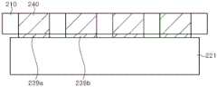
本发明的实施例中,说明了耦合层33d保护分布布拉格反射器133b,但也可以是前面说明的上绝缘层37覆盖分布布拉格反射器133b的顶面以及侧面而保护分布布拉格反射器133b。进而,上绝缘层37可以由SiO2-TiO2混合层或MgF2层形成,可以省略耦合层33d。In the embodiment of the present invention, the
图10是用于说明本发明另一实施例的发光二极管的概要截面图。图10是放大示出基板21的边缘部分的截面图。10 is a schematic cross-sectional view of a light emitting diode for explaining another embodiment of the present invention. FIG. 10 is an enlarged cross-sectional view showing an edge portion of the
参照图10,本实施例的发光二极管与参照图1以及图2而说明的发光二极管大体类似,其区别在于上绝缘层37覆盖下绝缘层33的侧面。Referring to FIG. 10 , the light emitting diode of this embodiment is generally similar to the light emitting diode described with reference to FIGS. 1 and 2 , and the difference is that the upper insulating
如图所示,第一导电型半导体层23形成为使基板21的边缘部分暴露。As shown in the drawing, the first conductive
下绝缘层33可以覆盖第一导电型半导体层23的侧面,但并不限于此,下绝缘层33的边缘也可以位于第一导电型半导体层23上。下绝缘层33的边缘可以位于第一焊盘金属层35a的外侧。如图所示,外部接触部35a1可以位于下绝缘层33的开口部33a1内。The lower insulating
上绝缘层37可以与下绝缘层33的侧面相接,进而可以与下绝缘层33的一部分顶面相接。The upper insulating
在本实施例中,下绝缘层33可以与参照图3或者图6而说明的情况相同,但并不限于此,也可以是包括以往技术的分布布拉格反射器的情况(例如,表现出图5中用虚线示出的反射率的下绝缘层)。In the present embodiment, the lower insulating
另一方面,当下绝缘层33包括以往技术的分布布拉格反射器时,上绝缘层37可以由SiO2-TiO2混合层或者MgF2层形成,由此,可以防止水分向分布布拉格反射器内渗透。On the other hand, when the lower insulating
图11是用于说明本发明另一实施例的发光二极管的概要俯视图,图12是用于说明图11的发光二极管的概要电路图,图13是沿着图11的截取线B-B截取的概要截面图,图14是沿着图11的截取线C-C截取的概要截面图。11 is a schematic plan view of a light emitting diode for explaining another embodiment of the present invention, FIG. 12 is a schematic circuit diagram for explaining the light emitting diode of FIG. 11 , and FIG. 13 is a schematic cross-sectional view taken along line B-B of FIG. 11 . 14 is a schematic cross-sectional view taken along the interception line C-C of FIG. 11 .
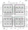
参照图11至图14,本实施例的发光二极管与前面说明的实施例大体类似,其区别在于在基板21上排列多个发光单元C1、C2、C3、C4。如图12所示,这些发光单元C1、C2、C3、C4可以在第一凸块焊盘39a和第二凸块焊盘39b之间串联连接。Referring to FIGS. 11 to 14 , the light emitting diode of this embodiment is generally similar to the embodiment described above, and the difference lies in that a plurality of light emitting units C1 , C2 , C3 , and C4 are arranged on the
第一发光单元C1、第二发光单元C2、第三发光单元C3以及第四发光单元C4布置在基板21上。第一发光单元C1、第二发光单元C2、第三发光单元C3以及第四发光单元C4通过使基板21暴露的分离区域彼此隔开。可以在发光单元之间的区域中暴露基板21的顶面。The first light emitting unit C1 , the second light emitting unit C2 , the third light emitting unit C3 and the fourth light emitting unit C4 are arranged on the
在本实施例中,示出第一发光单元C1以及第二发光单元C2布置在下方,第三发光单元C3以及第四发光单元C4布置在上方,但是第一发光单元C1、第二发光单元C2、第三发光单元C3以及第四发光单元C4可以以各种方式排列。另外,在本实施例中,示出并说明了四个发光单元排列在基板21上,但是发光单元的数量不特别限制。例如,在基板21上可以布置两个发光单元,也可以布置七个发光单元。In this embodiment, it is shown that the first light emitting unit C1 and the second light emitting unit C2 are arranged below, the third light emitting unit C3 and the fourth light emitting unit C4 are arranged above, but the first light emitting unit C1 and the second light emitting unit C2 , the third light emitting unit C3 and the fourth light emitting unit C4 may be arranged in various ways. In addition, in the present embodiment, four light-emitting units are shown and described as being arranged on the
各发光单元包括第一导电型半导体层23以及台面M。第一电型半导体层23以及台面M与前面参照图1以及图2而说明的情况相同,因此为了避免重复,省略对相同事项的详细说明。Each light emitting unit includes the first conductive
台面M可以限定在被第一导电型半导体层23围绕的区域内侧,因此,与第一导电型半导体层23的外侧面相邻的边缘附近区域不被台面M覆盖而暴露在外部。The mesas M may be defined inside the region surrounded by the first conductive
在本实施例中,各台面M可以包括过孔27a,第一导电型半导体层23在过孔27a内暴露。In this embodiment, each of the mesas M may include a via
另一方面,在各台面M上布置导电性氧化物层28,介电层29覆盖各个发光单元C1、C2、C3、C4上的导电性氧化物层28以及台面M。导电性氧化物层28与第二导电型半导体层27欧姆接触。导电性氧化物层28可以在台面M上方区域跨台面M的几乎整个区域而布置。只是,导电性氧化物层28可以与台面M的边缘隔开。On the other hand, a
介电层29可以覆盖台面M上方区域以及侧面,并覆盖暴露在台面M周围的第一导电型半导体层。介电层29还具有使得导电性氧化物层28暴露的开口部29a。介电层29位于第一导电型半导体层23的上方区域内,因此,彼此不同的发光单元上的介电层29可以彼此隔开。但是,本发明并不是必须限于此,相邻的发光单元上的介电层也可以彼此连接。The
金属反射层31布置在介电层29上,通过介电层29的开口部29a与导电性氧化物层28接通。金属反射层31布置在各发光单元C1、C2、C3、C4的台面M上方区域内。The metal
下绝缘层33覆盖台面M并覆盖金属反射层31以及介电层29。下绝缘层33还覆盖暴露在介电层29外部的第一导电型半导体层23以及基板21。当基板21为图案化的蓝宝石基板时,下绝缘层33可以沿着基板21上的凸出部的形状形成。The lower insulating
如图所示,下绝缘层33的边缘可以位于各发光单元的第一导电型半导体层23上,但并不限于此,可以覆盖第一导电型半导体层23的侧面并位于基板21上。As shown in the figure, the edge of the lower insulating
下绝缘层33具有在各台面M的过孔27a内使得第一导电型半导体层23暴露的第一开口部33a,还具有在第一发光单元C1上使得金属反射层31暴露的第二开口部33b1以及在第二发光单元C2、第三发光单元C3以及第四发光单元C4上使得金属反射层31暴露的第二开口部33b2。The lower insulating
在本实施例中,下绝缘层33不包括使得台面M周围的第一导电型半导体层23暴露的开口部。但是,本发明并不限于此,下绝缘层33也可以包括使得台面周围的第一导电型半导体层23暴露的开口部。In the present embodiment, the lower insulating
第二开口部33b1布置在第一发光单元C1上,第二开口部33b2在发光单元的分离区域附近中使得各发光单元的金属反射层31暴露。第二开口部33b2可以具有大体上沿着分离区域长的形状,但并不限于此,可以具有各种形状。The second opening portion 33b1 is arranged on the first light emitting cell C1, and the second opening portion 33b2 exposes the
另一方面,第二开口部33b1可以位于第一发光单元C1上,并位于第二凸块焊盘39b下方区域内。但是,在另一实施例中,第二开口部33b1也可以在第一发光单元C1上在水平方向上与第二凸块焊盘39b隔开布置。On the other hand, the second opening portion 33b1 may be located on the first light emitting cell C1 and located in a region under the
另一方面,第一焊盘金属层35a、第二焊盘金属层35b以及连接金属层35c布置在下绝缘层33上。On the other hand, the first
第一焊盘金属层35a布置在第四发光单元C4上,与暴露在台面M的过孔27a内的第一导电型半导体层23欧姆接触。在本实施例中,示出在过孔27a内形成内部接触部,但是在台面M周围上也可以形成外部接触部。只是,通过将第一焊盘金属层35a布置在台面M的上方区域内,可以使得远离基板21的边缘,由此,可以防止第一焊盘金属层35a因从基板21的侧面一侧进入的水分受到损伤。The first
第二焊盘金属层35b可以布置在第一发光单元C1上,并通过第二开口部33b1与金属反射层31电接通。由此,第二焊盘金属层35b与第一发光单元C1的第二导电型半导体层27电接通。The second
第二焊盘金属层35b位于台面M上,与第一导电型半导体层23绝缘。进而,第二焊盘金属层35b可以与第一发光单元C1上的台面M的侧面隔开。由此,可以防止第二焊盘金属层35b因从基板21的侧面一侧进入的水分受到损伤。The second
另一方面,连接金属层35c将相邻的发光单元彼此串联连接。连接金属层35c可以通过下绝缘层33的第一开口部33a以及第二开口部33b2与相邻的发光单元的第一导电型半导体层23以及第二导电型半导体层27电接通。例如,一个连接金属层35c可以与第一发光单元C1中的第一导电型半导体层23电接通,同时与第二发光单元C2上的金属反射层31电接通。由此,第一发光单元C1和第二发光单元C2通过连接金属层33c彼此串联连接。如此,第二发光单元C2和第三发光单元C3可以通过连接金属层35c串联连接,第三发光单元C3和第四发光单元C4可以通过连接金属层35c串联连接。On the other hand, the
连接金属层35c与第一焊盘金属层35a以及第二焊盘金属层35b隔开。进而,连接金属层35c可以形成为具有比台面M窄的宽度,因此,可以比台面M更远离基板21的边缘。The
第一焊盘金属层35a、第二焊盘金属层35b以及连接金属层35c可以通过相同工艺并以相同材料一起形成。例如,第一焊盘金属层35a、第二焊盘金属层35b以及连接金属层35c可以包括Al层之类欧姆反射层,欧姆反射层可以形成在Ti、Cr或者Ni等的粘合层上。另外,可以在所述欧姆反射层上形成Ni、Cr、Au等的单层或者复合层结构的保护层。第一焊盘金属层35a、第二焊盘金属层35b以及连接金属层35c例如可以具有Cr/Al/Ni/Ti/Ni/Ti/Au/Ti的多层结构。The first
上绝缘层37布置在第一焊盘金属层35a、第二焊盘金属层35b以及连接金属层35c上,具有使得第一焊盘金属层35a暴露的第一开口部37a以及使得第二焊盘金属层35b暴露的第二开口部37b。上绝缘层37可以覆盖暴露在发光单元21周围的基板21顶面。如图所示,上绝缘层37可以覆盖基板21的边缘,但并不限于此,上绝缘层37的边缘可以位于基板21的边缘内侧。The upper insulating
另一方面,所述第一开口部37a布置在第一焊盘金属层35a的上方区域内,因此,与连接金属层35c以及下绝缘层33的第二开口部33b2隔开。另外,所述第二开口部37b还限定并存在于第二焊盘金属层35b上,与连接金属层35c隔开。On the other hand, the
在本实施例中,通过上绝缘层37的第一开口部37a以及第二开口部37b暴露的所述第一焊盘金属层35a以及第二焊盘金属层35b可以用作直接焊接焊锡的焊接盘。与此不同,如参照图1以及图2而说明的那样,第一凸块焊盘39a以及第二凸块焊盘39b可以分别覆盖通过上绝缘层37的第一开口部37a以及第二开口部37b暴露的第一焊盘金属层35a以及第二焊盘金属层35b。所述第一凸块焊盘39a以及第二凸块焊盘39b可以分别跨多个发光单元而布置,覆盖并密封第一开口部37a以及第二开口部37b。In this embodiment, the first
在本实施例中,下绝缘层33可以是参照图3而说明的下绝缘层,但并不限于此,也可以是参照图6而说明的下绝缘层33′。另外,也可以是参照图9a或者图9b而说明的下绝缘层。进而,下绝缘层33可以是包括以往的分布布拉格反射器的下绝缘层,此时,上绝缘层37可以包括SiO2-TiO2混合层或者MgF2层。In this embodiment, the lower insulating
另一方面,将由SiO2-TiO2混合层形成的耦合层33d和适用图7的分布布拉格反射器的下绝缘层33′适用到包括多个发光单元的发光二极管,在温度85℃及相对湿度85%,温度60℃及相对湿度90%的高温高湿环境下执行可靠性测试。另一方面,将图5的以往技术的下绝缘层适用到包括所述多个发光单元的发光二极管,在相同条件下执行可靠性测试。On the other hand, applying the
以往技术的式样经500小时,大部分的发光二极管发生不良,中止了可靠性测试,但是,本发明实施例的式样在两个条件下直到2000小时,不良发生率均未超过5%。After 500 hours in the prior art model, most of the light-emitting diodes failed and the reliability test was terminated. However, the model of the present invention did not exceed 5% of the failure rate until 2000 hours under both conditions.
因此,可以确认通过使用SiO2-TiO2混合层而高温高湿环境下的可靠性提高。Therefore, it was confirmed that reliability in a high temperature and high humidity environment was improved by using the SiO2 -TiO2 mixed layer.
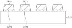
图15是用于说明本发明一实施例的发光二极管1000的概要俯视图,图16是沿着图15的截取线A-A截取的截面图。FIG. 15 is a schematic plan view illustrating a
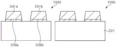
参照图15以及图16,所述发光二极管可以包括基板221、第一导电型半导体层223、活性层225、第二导电型半导体层227、导电性氧化物层228、介电层229、金属反射层231、下绝缘层233、第一焊盘金属层235a、第二焊盘金属层235b、上绝缘层237、第一凸块焊盘239a、第二凸块焊盘239b、第一焊锡凸块241a以及第二焊锡凸块241b。15 and 16 , the light emitting diode may include a
所述基板221只要是能够使氮化镓系半导体层生长的基板,不特别限制。作为基板221的例子,可以是蓝宝石基板、氮化镓基板、SiC基板等各种基板,可以是图案化的蓝宝石基板。基板221可以如图15的俯视图那样具有矩形或者正方形的外形,但不是必须限于此。基板221的尺寸不特别限制,可以多样地选择。The
第一导电型半导体层223布置在基板221上。第一导电型半导体层223是在基板221上生长的层,可以是氮化镓系半导体层。第一导电型半导体层223可以是掺杂有掺杂,例如Si的氮化镓系半导体层。The first conductive
在本实施例中,第一导电型半导体层223的边缘可以位于被基板221的边缘围绕的区域内侧。由此,基板221的上表面中的一部分区域可以沿着第一导电型半导体层223的缘边暴露。但是,本发明并不限于此,第一导电型半导体层223的边缘也可以与基板221的边缘并肩。In this embodiment, the edge of the first conductive
台面M可以布置在第一导电型半导体层223上。台面M可以限定并存在于被第一导电型半导体层223围绕的区域内侧,因此,第一导电型半导体层223的边缘附近区域可以不被台面M覆盖而暴露在外部。The mesas M may be arranged on the first conductive
台面M包括第二导电型半导体层227和活性层225。虽未图示,台面M也可以包括第一导电型半导体层223的一部分厚度。所述活性层225介于第一导电型半导体层223和第二导电型半导体层227之间。活性层225可以具有单量子阱结构或者多量子阱结构。在活性层225内,阱层的组成以及厚度决定所生成的光的波长。尤其,可以通过调整阱层的组成来提供生成紫外线、青色光或者绿色光的活性层。The mesa M includes the second conductive
另一方面,第二导电型半导体层227可以是掺杂有p型掺杂,例如Mg的氮化镓系半导体层。第二导电型半导体层227中的p型掺杂浓度可以具有在所述范围内根据厚度变化的浓度分布。On the other hand, the second conductive
另一方面,第一导电型半导体层223以及第二导电型半导体层22可以分别是单层,但并不限于此,也可以是多重层,也可以包括超晶格层。第一导电型半导体层223、活性层225以及第二导电型半导体层227可以利用金属有机化学气相沉积法(MOCVD)或者分子束外延(MBE)等的公知方法在腔室内在基板221上生长而形成。On the other hand, the first-conductivity-
另一方面,如图15所示,所述台面M上可以具有使第一导电型半导体层223暴露的过孔227a。过孔227a可以被第二导电型半导体层227以及活性层225围绕。如图15所示,过孔227a可以具有经过发光二极管中心的长的形状。如图所示,过孔227a可以布置为经过台面M的中心,向一侧边缘侧倾斜。过孔227a的长度不特别限制,可以是台面M长度的1/2或者比其长。On the other hand, as shown in FIG. 15 , the mesas M may have via
另一方面,如图所示,过孔227a的两侧端部可以宽度相对宽并具有圆形形状。通过如此设置过孔227a的末端部形状,可以以类似的形状对介电层229以及下绝缘层233进行图案化。尤其,当下绝缘层233包括分布布拉格反射器时,如果并未如图15那样在过孔227a的末端部处宽度变宽,则在分布布拉格反射器的侧壁形成严重的双台阶,侧壁的倾斜角变大,因此在第一焊盘金属层235a中容易发生破裂。因此,通过如本实施例那样构成过孔227a的末端部形状以及下绝缘层233的第一开口部233a2的末端部形状,下绝缘层233的边缘可以具有平缓的倾斜角,可以改善发光二极管的产率。On the other hand, as shown in the drawing, both side end portions of the via
示出并说明了台面M具有单一的过孔227a,但本发明并不限于此。例如,在台面M内部也可以排列多个过孔。过孔227a的数量约增加,越能改善发光二极管的电流分散性能。另外,也可以在台面M缘边形成向台面M内部进入的凸伸部而代替过孔227a。凸伸部可以从台面M的一侧边缘朝向与其对置的另一侧边缘,向台面M内部长长地形成。It is shown and described that the mesa M has a single via
另一方面,导电性氧化物层228布置在台面M上方而与第二导电型半导体层227接触。导电性氧化物层228可以在台面M上方区域中跨台面M的几乎整个区域而布置。例如,导电性氧化物层228可以覆盖台面M上方区域的80%以上,进而90%以上。On the other hand, the
导电性氧化物层228由使得在活性层225生成的光透过的氧化物层形成。导电性氧化物层228例如可以由ITO(铟锡氧化物)或者ZnO等形成。导电性氧化物层228以足以与第二导电型半导体层227欧姆接触的厚度形成,例如可以在3nm至50nm厚度范围内,具体地在6nm至30nm的厚度范围内形成。如果导电性氧化物层228的厚度过薄,则无法提供充分的欧姆特性,正向电压增加。另外,如果导电性氧化物层228的厚度过厚,则发生光吸收引起的损失,降低发光效率。The
另一方面,介电层229覆盖导电性氧化物层228。进而,介电层229可以覆盖第二导电型半导体层227以及活性层225的侧面。介电层229的边缘可以由下绝缘层233覆盖。因此,与下绝缘层233的边缘相比,介电层229的边缘更远离基板221的边缘。由此,如后面所述,下绝缘层233的一部分可以在台面M周围与第一导电型半导体层223相接。进一步,介电层229可以限定在第二导电型半导体层227的上方区域内,下绝缘层233也可以与第二导电型半导体层227以及活性层225的侧面相接。On the other hand, the
介电层229具有使得导电性氧化物层228暴露的开口部229a。多个开口部229a可以布置在导电性氧化物层228上方。开口部229a可以用作接通通道,以使金属反射层231能够与导电性氧化物层228接通。介电层229可以还具有在台面M周围使得第一导电型半导体层223暴露并在过孔227a内使得第一导电型半导体层223暴露的开口部229b。The
介电层229由具有比第二导电型半导体层227以及导电性氧化物层228低的折射率的绝缘物质形成。介电层229例如可以由SiO2形成。The
介电层229的厚度可以具有200nm至1000nm范围内的厚度,具体地可以具有300nm至800nm范围内的厚度。当介电层229的厚度小于200nm时,正向电压高且光输出低而不理想。另一方面,若介电层229厚度超过400nm,则光输出饱和,显示出正向电压再次增加的趋势。因此,优选的是介电层229的厚度不超过1000nm,尤其可以是800nm以下。The thickness of the
另一方面,金属反射层231布置在介电层229上而通过开口部229a与欧姆接触层228接通。金属反射层231可以包含反射性金属,例如可以包含Ag或者Ni/Ag。进而,金属反射层232可以包括用于保护反射金属物质层的障壁层,例如Ni,另外,为了防止金属层的氧化,可以包括Au层。进而,为了提高Au层的粘合力,也可以在Au层下方包括Ti层。金属反射层231与介电层229的顶面相接,因此,所述介电层229的厚度与导电性氧化物层228和金属反射层231之间的隔开距离相同。On the other hand, the
由导电性氧化物层228形成欧姆接触,在介电层229上布置金属反射层231,从而可以防止焊锡等导致的欧姆电阻变高。进而,可以通过将导电性氧化物层228、介电层229以及金属反射层231布置在第二导电型半导体层227上而提高光的反射率,从而可以改善发光效率。The ohmic contact is formed by the
下绝缘层233覆盖台面M以及金属反射层231。下绝缘层233可以还沿着台面M缘边覆盖第一导电型半导体层223,可以在台面M内部的过孔227a内覆盖第一导电型半导体层223。下绝缘层233尤其覆盖台面M的侧面。下绝缘层233可以还覆盖介电层229。The lower
另一方面,下绝缘层233具有使得第一导电型半导体层暴露的第一开口部233a1、233a2以及使得金属反射层231暴露的第二开口部233b。第一开口部233a1沿着台面M缘边使得第一导电型半导体层223暴露,第一开口部233a2在所述过孔227a内使得第一导电型半导体层223暴露。On the other hand, the lower insulating
如图15所示,可以沿着台面M缘边排列多个第一开口部233a1,但本发明并不限于此。例如,也可以沿着台面M缘边形成单一的第一开口部233a1。As shown in FIG. 15 , a plurality of first openings 233a1 may be arranged along the edge of the mesa M, but the present invention is not limited thereto. For example, a single first opening 233a1 may be formed along the edge of the mesa M.
在本实施例中,示出并说明了沿着台面M缘边布置下绝缘层233的第一开口部233a1,但是下绝缘层233也可形成为将包括第一导电型半导体层223的边缘在内的其周边区域均暴露。即,在本实施例中,示出了下绝缘层233的边缘与基板221的边缘并肩,但是下绝缘层233的边缘可以位于第一导电型半导体层223上。In the present embodiment, the first opening portion 233a1 of the lower insulating
第二开口部233b使得金属反射层231暴露。可以形成多个第二开口部233b,这些第二开口部233b可以布置在台面M的中央区域附近。The
另一方面,下绝缘层233可以由SiO2或者Si3N4的单层形成,但并不限于此,也可以由多重层形成。进而,下绝缘层233可以包括分布布拉格反射器。分布布拉格反射器可以层叠折射率彼此不同的绝缘层而形成。例如,分布布拉格反射器可以交替重复层叠硅氧化膜和钛氧化膜而形成。下绝缘层233可以还包括耦合层。耦合层可以覆盖分布布拉格反射器的顶面而作为保护分布布拉格反射器的保护层发挥功能。另外,耦合层提高布置在分布布拉格反射器上的焊盘金属层235a、235b的粘合力。所述耦合层可以由SiO2形成,但并不限于此,也可以由SiO2-TiO2混合层或者MgF2层形成。SiO2-TiO2混合层或者MgF2层具有防水特性,因此提高发光二极管在高温高湿环境下的可靠性。On the other hand, the lower insulating
另一方面,第一焊盘金属层235a布置在所述下绝缘层233上,通过下绝缘层233相对于台面M以及金属反射层231绝缘。第一焊盘金属层235a通过下绝缘层233的第一开口部233a1、233a2与第一导电型半导体层223接触。第一焊盘金属层235a可以沿着台面M缘边通过第一开口部233a1与第一导电型半导体层223接触,另外,可以通过第二开口部233a2在过孔227a内与第一导电型半导体层223接触。On the other hand, the first
另一方面,第二焊盘金属层235b在下绝缘层233上布置在台面M上方区域,通过下绝缘层233的第二开口部233b与金属反射层231电接通。第二焊盘金属层235b可以被第一焊盘金属层235a围绕,在它们之间可以形成边界区域。如图15所示,边界区域可以形成为环形状。下绝缘层233在边界区域中暴露,该边界区域由后述的上绝缘层237覆盖。On the other hand, the second
第一焊盘金属层235a和第二焊盘金属层235b可以通过相同工艺以相同材料一起形成。第一焊盘金属层235a以及第二焊盘金属层235b可以包括Al层之类欧姆反射层,欧姆反射层可以形成在Ti、Cr或者Ni等的粘合层上。另外,可以在所述欧姆反射层上形成Ni、Cr、Au等的单层或者复合层结构的保护层。第一焊盘金属层235a以及第二焊盘金属层235b例如可以具有Cr/Al/Ni/Ti/Ni/Ti/Au/Ti的多层结构。The first
上绝缘层237覆盖第一焊盘金属层235a以及第二焊盘金属层235b。另外,上绝缘层237可以沿着台面M缘边覆盖第一导电型半导体层223。在本实施例中,上绝缘层237与基板221的边缘并肩。但是,本发明并不限于此,上绝缘层237的边缘也可以位于被基板221的边缘围绕的区域内侧,以便上绝缘层237使基板221的边缘区域暴露。The upper insulating
另一方面,上绝缘层237具有使得第一焊盘金属层235a暴露的第一开口部237a以及使得第二焊盘金属层235b暴露的第二开口部237b。第一开口部237a以及第二开口部237b可以布置在台面M上方区域,可以布置为彼此对置。尤其,第一开口部237a以及第二开口部237b可以布置为接近台面M的两侧边缘。另外,如图所示,上绝缘层237的第二开口部237b可以与下绝缘层233的第二开口部233b横向隔开。通过使得下绝缘层233的第二开口部233b和上绝缘层237的第二开口部237b横向隔开,可以防止焊锡引起金属反射层231以及导电性氧化物层228损伤。On the other hand, the upper insulating
上绝缘层237可以由SiO2或者Si3N4的单层形成,但并不限于此,也可以包括SiO2-TiO2混合层或者MgF2层。SiO2-TiO2混合层或者MgF2层的防水特性优异,可以提高发光二极管在高温高湿环境下的可靠性。另外,上绝缘层237既也可以具有包括硅氮化膜和硅氧化膜的多层结构,也可以包括交替层叠硅氧化膜和钛氧化膜的分布布拉格反射器。The upper insulating
另一方面,第一凸块焊盘239a与通过上绝缘层237的第一开口部237a暴露的第一焊盘金属层235a电接触,第二凸块焊盘239b与通过第二开口部237b暴露的第二焊盘金属层235b电接触。如图15所示,第一凸块焊盘239a以及第二凸块焊盘239b可以分别将上绝缘层237的第一开口部237a以及第二开口部237b全部覆盖并密封。但是,本发明并不限于此,可以是第一凸块焊盘239a布置在上绝缘层237的第一开口部237a内,第二凸块焊盘239b布置在上绝缘层237的第二开口部237b内。On the other hand, the
另外,如图15所示,第二凸块焊盘239b可以限定并存在于第二焊盘金属层235a的上方区域内。但是,本发明并不限于此,第二凸块焊盘239b的一部分也可以与第一焊盘金属层235a重叠。只是,上绝缘层237可以布置在第一焊盘金属层235a和第二凸块焊盘239b之间而使它们绝缘。In addition, as shown in FIG. 15, a
第一凸块焊盘239a以及第二凸块焊盘239b可以由金属层形成,可以包括多个层。尤其,第一凸块焊盘239a以及第二凸块焊盘239b可以包含Au或者Pt。The
第一焊锡凸块241a布置在第一凸块焊盘239a上,第二焊锡凸块241b布置在第二凸块焊盘239b上。第一焊锡凸块241a以及第二焊锡凸块241b例如可以包括AgCuSn。The
第一焊锡凸块241a以及第二焊锡凸块241b可以分别如下形成:在第一凸块焊盘239a以及第二凸块焊盘239b上布置包括焊锡粉末和钎剂的焊锡膏之后利用回流工艺去除钎剂。由此,第一焊锡凸块241a以及第二焊锡凸块241b可以分别具有与第一凸块焊盘239a、第二凸块焊盘239b的面积相同的底部面积。The
另一方面,与第一凸块焊盘239a以及第二凸块焊盘239b相比,第一焊锡凸块241a以及第二焊锡凸块241b相对厚。例如,第一焊锡凸块241a或者第二焊锡凸块241b的厚度T2可以是第一凸块焊盘239a或者第二凸块焊盘239b的厚度T1的10倍至80倍。具体地,所述第一凸块焊盘239a以及第二凸块焊盘239b具有大致1um程度的厚度,与此相反,第一焊锡凸块241a以及第二焊锡凸块241b可以具有10um至100um的厚度。On the other hand, the
另外,第一焊锡凸块241a以及第二焊锡凸块241b可以具有倾斜的侧面,可以具有大致梯形的截面形状。如图17所示,第一焊锡凸块241a以及第二焊锡凸块241b的侧面相对于底面的倾斜角θ可以在约65度至75度范围内。当倾斜角θ在上述范围内时,可以容易形成焊锡凸块241a、241b,进而,可以容易地转移(transfer)发光二极管1000。In addition, the
另一方面,如图18所示,需要控制第一焊锡凸块241a和第二焊锡凸块241b之间的间隔s1、第一焊锡凸块241a以及第二焊锡凸块241b和基板221边缘之间的间隔s2、s3。例如,间隔s1是第一焊锡凸块241a以及第二焊锡凸块241b的厚度的2倍以上。间隔s1的上限不特别限制,但是为了确保焊锡凸块241a、焊锡凸块241b的足够面积,可以不超过10倍。On the other hand, as shown in FIG. 18, it is necessary to control the interval s1 between the
另一方面,间隔s2、s3可以是间隔s1的1/2以上。进而,间隔s2、s3可以与第一焊锡凸块241a以及第二焊锡凸块241b的厚度T2相同或者比其大。通过控制间隔s1、s2、s3,可以利用丝网印刷技术容易地形成第一焊锡凸块241a以及第二焊锡凸块241b,可以防止焊锡凸块之间的电短路。On the other hand, the intervals s2 and s3 may be 1/2 or more of the interval s1. Furthermore, the intervals s2 and s3 may be the same as or larger than the thickness T2 of the
根据本发明的实施例,使用导电性氧化物层228、介电层229以及金属反射层231的反射结构而代替以往的欧姆反射层。由此,可以阻断焊锡等的焊接材料进入到接触区域,可以确保稳定的欧姆接触电阻,从而可以提高发光二极管的可靠性。进而,通过将介电层229的厚度设为300nm以上,可以实现高的光输出以及低的正向电压。According to the embodiment of the present invention, the reflective structure of the
进而,通过在第一凸块焊盘239a以及第二凸块焊盘239b上形成第一焊锡凸块241a以及第二焊锡凸块241b,可以减少在发光二极管的安装工艺中使用的焊锡膏的量,可以简化发光二极管安装工艺。Furthermore, by forming the
另外,通过布置与第一凸块焊盘239a以及第二凸块焊盘239b相比具有10倍以上厚度的焊锡凸块241a、241b,可以容易地进行发光二极管的操纵。In addition, by arranging the solder bumps 241a, 241b having a
图19a至图19f是用于说明本发明一实施例的发光元件制造工艺的概要截面图。在此,说明利用丝网印刷技术形成焊锡凸块241a、241b并利用其在安装面上进行安装的工艺。19a to 19f are schematic cross-sectional views for explaining a manufacturing process of a light-emitting element according to an embodiment of the present invention. Here, the process of forming the solder bumps 241a and 241b by the screen printing technique and mounting them on the mounting surface will be described.
首先,参照图19a,准备形成有凸块焊盘239a、239b的基板221。虽未图示,可以在基板221上形成如参照图15以及图16所说明那样的第一导电型半导体层223、活性层225、第二导电型半导体层227、导电性氧化物层228、介电层229、金属反射层231、下绝缘层233、第一焊盘金属层235a、第二焊盘金属层235b以及上绝缘层237。可以在上绝缘层237上布置第一凸块焊盘239a以及第二凸块焊盘239b。First, referring to FIG. 19a, a
可以在基板221上布置多个发光二极管区域,在各区域中可以形成第一凸块焊盘239a以及第二凸块焊盘239b。A plurality of light emitting diode regions may be arranged on the
参照图19b,在基板221上布置掩模210。掩模210具有使得凸块焊盘239a、239b暴露的开口部,掩模210布置为开口部与凸块焊盘239a、239b对齐。开口部的高度可以是约20um以上,可以是约300um以下。Referring to FIG. 19b , the
接着,焊锡膏240填满掩模210的开口部。可以例如利用挤压印刷(SqueezePrinting)技术来涂布焊锡膏240。由此,具有大致与开口部的高度相对应的厚度的焊锡膏240布置在凸块焊盘上。Next, the
参照图19c,去除掩模210,通过回流工艺使焊锡膏回流。由此,焊锡膏凝结而形成具有侧面倾斜且顶面鼓起形状的焊锡凸块240a。在回流工艺中,可以去除焊锡膏中的大部分钎剂。Referring to FIG. 19c, the
为了去除掩模210,需要将焊锡膏240之间的间隔设成焊锡膏240的厚度以上。若焊锡膏240之间的间隔过窄,则焊锡膏240可能彼此连接,难以去除掩模210。In order to remove the
另一方面,在回流工艺中,第一凸块焊盘239a以及第二凸块焊盘239b和焊锡还可能彼此扩散而混合。由此,也可能导致第一凸块焊盘239a以及第二凸块焊盘239b和焊锡凸块240a之间的边界不清楚。只是,当第一凸块焊盘239a以及第二凸块焊盘239b由多层金属层形成时,可以是一部分与焊锡混合而一部分残留。On the other hand, in the reflow process, the
参照图19d,去除焊锡凸块240a的厚度一部分而形成第一焊锡凸块241a以及第二焊锡凸块241b。可以例如利用飞剪(Flying Cut)技术之类切削工艺来切削焊锡凸块240a。19d, a part of the thickness of the
尤其,焊锡凸块240a可以切削50%以上。由此,第一焊锡凸块241a以及第二焊锡凸块241b可以以掩模210的开口部的高度的1/2以下的厚度形成。在焊锡凸块240a的切削小于50%的情况下,当转移发光二极管时,由于焊锡凸块241a、241b的粘合力不良而容易发生工艺不良。In particular, the
参照图19e,通过分割基板221来完成个体发光二极管1000。可以在分割基板221之前增加磨削基板221的底面而减少厚度的工艺。减少基板221的厚度的工艺也可以在印刷焊锡膏之前执行。Referring to FIG. 19e , the individual
另一方面,图中示出形成两个发光二极管1000,但是可以在一个基板221上形成几百个或者几千个发光二极管1000。On the other hand, the figure shows that two light emitting
参照图19f,发光二极管1000焊接到具有接通焊盘251a、251b的基底基板251上。发光二极管1000的焊锡凸块241a、241b在接通焊盘251a、251b上对齐,可以通过利用回流工艺的焊接技术将发光二极管1000焊接到基底基板251上。19f, the
此时,可以预先在接通焊盘251a、251b上涂布焊锡膏。只是,随着焊锡凸块241a、241b布置在发光二极管1000上,与以往技术相比,可以大幅减少涂布在接通焊盘251a、251b上的焊锡膏的量。At this time, solder paste may be applied to the via
由此,提供通过焊锡241a′、241b′将接通焊盘251a、251b和第一凸块焊盘241a、第二凸块焊盘241b彼此焊接的发光元件。Thereby, a light-emitting element in which the
在此,虽然说明了发光二极管1000安装在基底基板251上,但是也可以使用印刷电路板而代替基底基板251,或者也可以使用具有引线的封装件。Here, although the
由此,可以提供安装有发光二极管1000的发光二极管封装件或者发光模组等各种发光元件。Thereby, various light-emitting elements such as a light-emitting diode package or a light-emitting module in which the light-emitting
图20是用于说明本发明另一实施例的发光二极管2000的概要俯视图,图21是用于说明图20的发光二极管的概要电路图,图22是沿着图20的截取线B-B截取的概要截面图,图23是沿着图20的截取线C-C截取的概要截面图。20 is a schematic plan view of a
参照图20至图23,本实施例的发光二极管与前面参照图15而说明的实施例大体类似,其区别在于在基板221上排列多个发光单元C1、C2、C3、C4。如图21所示,这些发光单元C1、C2、C3、C4可以在第一凸块焊盘239a和第二凸块焊盘239b之间串联连接。Referring to FIGS. 20 to 23 , the light emitting diode of this embodiment is generally similar to the embodiment described above with reference to FIG. 15 , the difference is that a plurality of light emitting units C1 , C2 , C3 , and C4 are arranged on the
在基板221上布置第一发光单元C1、第二发光单元C2、第三发光单元C3以及第四发光单元C4。通过使基板221暴露的分离区域,第一发光单元C1、第二发光单元C2、第三发光单元C3以及第四发光单元C4彼此隔开。基板221的顶面可以在发光单元之间的区域暴露。The first light emitting cell C1 , the second light emitting cell C2 , the third light emitting cell C3 and the fourth light emitting cell C4 are arranged on the
在本实施例中,示出第一发光单元C1以及第二发光单元C2布置在下侧,第三发光单元C3以及第四发光单元C4布置在上侧,但是第一发光单元C1、第二发光单元C2、第三发光单元C3以及第四发光单元C4可以以各种方式排列。另外,在本实施例中,示出并说明了四个发光单元排列在基板221上,但是发光单元的数量不特别限制。例如,在基板221上既可以布置两个发光单元,也可以布置七个发光单元。In this embodiment, it is shown that the first light emitting unit C1 and the second light emitting unit C2 are arranged on the lower side, and the third light emitting unit C3 and the fourth light emitting unit C4 are arranged on the upper side, but the first light emitting unit C1 and the second light emitting unit C4 are arranged on the upper side. The C2, the third light emitting unit C3, and the fourth light emitting unit C4 may be arranged in various ways. In addition, in the present embodiment, four light-emitting units are shown and described as being arranged on the
各发光单元包括第一导电型半导体层223以及台面M。第一导电型半导体层223以及台面M与前面参照图15以及图16而说明的情况相同,因此为了避免重复,省略对相同事项的详细说明。Each light emitting unit includes the first conductive
台面M可以限定并存在于被第一导电型半导体层223围绕的区域内侧,因此,与第一导电型半导体层223的外侧面相邻的边缘附近区域不被台面M覆盖而暴露在外部。The mesas M may be defined and present inside a region surrounded by the first conductive
在本实施例中,各台面M可以包括过孔227a,第一导电型半导体层223在各过孔227a内暴露。In this embodiment, each of the mesas M may include a via
另一方面,在各台面M上布置导电性氧化物层228,介电层229覆盖各个发光单元C1、C2、C3、C4上的导电性氧化物层228以及台面M。导电性氧化物层228与第二导电型半导体层227欧姆接触。导电性氧化物层228可以在台面M上方区域跨台面M的几乎整个区域而布置。只是,导电性氧化物层228可以与台面M的边缘隔开。On the other hand, a
介电层229可以覆盖台面M上方区域以及侧面,并覆盖暴露在台面M周围的第一导电型半导体层。介电层229还具有使得导电性氧化物层228暴露的开口部229a。介电层229位于第一导电型半导体层223的上方区域内,因此,彼此不同的发光单元上的介电层229可以彼此隔开。但是,本发明并不必须限于此,相邻的发光单元上的介电层也可以彼此连接。The
金属反射层231布置在介电层229上,通过介电层229的开口部229a与导电性氧化物层228接通。金属反射层231布置在各发光单元C1、C2、C3、C4的台面M上方区域内。The metal
下绝缘层233覆盖台面M并覆盖金属反射层231以及介电层229。下绝缘层233还覆盖暴露在介电层229外部的第一导电型半导体层223以及基板221。当基板221为图案化的蓝宝石基板时,下绝缘层233可以沿着基板221上的凸出部的形状形成。The lower
如图所示,下绝缘层233的边缘可以位于各发光单元的第一导电型半导体层223上,但并不限于此,也可以覆盖第一导电型半导体层223的侧面并位于基板221上。As shown in the figure, the edge of the lower insulating
下绝缘层233具有在各台面M的过孔227a内使得第一导电型半导体层223暴露的第一开口部233a,还具有在第一发光单元C1上使得金属反射层231暴露的第二开口部233b1以及在第二发光单元C2、第三发光单元C3以及第四发光单元C4上使得金属反射层231暴露的第二开口部233b2。The lower
在本实施例中,下绝缘层233不包括使得台面M周围的第一导电型半导体层223暴露的开口部。但是,本发明并不限于此,下绝缘层233也可以包括使得台面周围的第一导电型半导体层223暴露的开口部。In the present embodiment, the lower insulating
第二开口部233b1布置在第一发光单元C1上,第二开口部233b2在发光单元的分离区域附近使得各发光单元的金属反射层231暴露。第二开口部233b2可以具有大体上沿着分离区域长的形状,但并不限于此,可以具有各种形状。The second opening portion 233b1 is arranged on the first light emitting unit C1, and the second opening portion 233b2 exposes the
另一方面,第二开口部233b1可以位于第一发光单元C1上,并位于第二凸块焊盘239b下方区域内。但是,在另一实施例中,第二开口部233b1也可以在第一发光单元C1上在水平方向上与第二凸块焊盘239b隔开布置。On the other hand, the second opening part 233b1 may be located on the first light emitting cell C1 and located in the area under the
如参照图15以及图16而说明的那样,下绝缘层233可以形成为单层或者多重层,或者可以包括分布布拉格反射器。另外,下绝缘层233可以还包括覆盖所述分布布拉格反射器的耦合层。As explained with reference to FIGS. 15 and 16 , the lower insulating
另一方面,第一焊盘金属层235a、第二焊盘金属层235b以及连接金属层235c布置在下绝缘层233上。On the other hand, the first
第一焊盘金属层235a布置在第四发光单元C4上,与暴露在台面M的过孔227a内的第一导电型半导体层223欧姆接触。在本实施例中,示出了在过孔227a内第一焊盘金属层235a与第一导电型半导体层223接触,但是也可以在台面M周围与第一导电型半导体层223接触。只是,通过将第一焊盘金属层235a布置在台面M的上方区域内,可以远离基板221的边缘,由此,可以防止第一焊盘金属层235a因从基板221的侧面一侧进入的水分受到损伤。The first
第二焊盘金属层235b可以布置在第一发光单元C1上,并通过第二开口部233b1与金属反射层231电接通。由此,第二焊盘金属层235b与第一发光单元C1的第二导电型半导体层227电接通。The second
第二焊盘金属层235b位于台面M上,与第一导电型半导体层223绝缘。进而,第二焊盘金属层235b可以与第一发光单元C1上的台面M的侧面隔开。由此,可以防止第二焊盘金属层235b因从基板221的侧面一侧进入的水分受到损伤。The second
另一方面,连接金属层235c将相邻的发光单元彼此串联连接。连接金属层235c可以通过下绝缘层233的第一开口部233a以及第二开口部233b2与相邻的发光单元的第一导电型半导体层223以及第二导电型半导体层227电接通。例如,一个连接金属层235c可以与第一发光单元C1内的第一导电型半导体层223电接通,同时与第二发光单元C2上的金属反射层231电接通。由此,第一发光单元C1和第二发光单元C2通过连接金属层233c彼此串联连接。如此,第二发光单元C2和第三发光单元C3可以通过连接金属层235c串联连接,第三发光单元C3和第四发光单元C4可以通过连接金属层235c串联连接。On the other hand, the
连接金属层235c与第一焊盘金属层235a以及第二焊盘金属层235b隔开。进而,连接金属层235c可以形成为具有比台面M窄的宽度,因此,可以比台面M更远离基板221的边缘。The
第一焊盘金属层235a、第二焊盘金属层235b以及连接金属层235c可以通过相同工艺以相同材料一起形成。例如,第一焊盘金属层235a、第二焊盘金属层235b以及连接金属层235c可以包括Al层之类欧姆反射层,欧姆反射层可以形成在Ti、Cr或者Ni等的粘合层上。另外,可以在所述欧姆反射层上形成Ni、Cr、Au等的单层或者复合层结构的保护层。第一焊盘金属层235a、第二焊盘金属层235b以及连接金属层235c例如可以具有Cr/Al/Ni/Ti/Ni/Ti/Au/Ti的多层结构。The first
上绝缘层237布置在第一焊盘金属层235a、第二焊盘金属层235b以及连接金属层235c上,并具有使得第一焊盘金属层235a暴露的第一开口部237a以及使得第二焊盘金属层235b暴露的第二开口部237b。上绝缘层237可以覆盖暴露在发光单元221周围的基板221顶面。如图所示,上绝缘层237可以覆盖基板221的边缘,但并不限于此,上绝缘层237的边缘也可以位于基板221的边缘内侧。The upper insulating
另一方面,所述第一开口部237a布置在第一焊盘金属层235a的上方区域内,因此,与连接金属层235c以及下绝缘层233的第二开口部233b2隔开。另外,所述第二开口部237b限定并存在于第二焊盘金属层235b上,与连接金属层235c隔开。On the other hand, the
在本实施例中,通过上绝缘层237的第一开口部237a以及第二开口部237b暴露的所述第一焊盘金属层235a以及第二焊盘金属层235b可以用作在其之上形成焊锡凸块241a、241b的凸块焊盘。与此不同,如参照图15以及图16而说明的那样,第一凸块焊盘239a以及第二凸块焊盘239b可以分别覆盖通过上绝缘层237的第一开口部237a以及第二开口部237b暴露的第一焊盘金属层235a以及第二焊盘金属层235b。所述第一凸块焊盘239a以及第二凸块焊盘239b可以分别跨多个发光单元而布置,可以覆盖并密封第一开口部237a以及第二开口部237b。In this embodiment, the first
第一焊锡凸块241a以及第二焊锡凸块241b分别布置在第一凸块焊盘239a以及第二凸块焊盘239b上。第一焊锡凸块241a以及第二焊锡凸块241b可以具有与第一凸块焊盘239a以及第二凸块焊盘239b相同形状的底面。另一方面,第一焊锡凸块241a及第二焊锡凸块241b的厚度、它们之间的间隔以及它们和基板221边缘之间的间隔与参照图17以及图18而说明的情况相同,因此为了避免重复,省略详细说明。The
图24以及图25是用于说明本发明另一实施例的发光二极管200a、200b的概要俯视图。24 and 25 are schematic plan views of light emitting diodes 200a and 200b for explaining another embodiment of the present invention.
参照图24,本实施例的发光二极管200a与参照图20至图23而说明的发光二极管大体类似,其区别在于第一凸块焊盘239a以及第二凸块焊盘239b的形状不同,由此,第一焊锡凸块241a以及第二焊锡凸块241b的形状存在差异。Referring to FIG. 24 , the light emitting diode 200 a of this embodiment is generally similar to the light emitting diode described with reference to FIGS. 20 to 23 , and the difference lies in that the shapes of the
即,在发光二极管2000中,第一凸块焊盘239a以及第二凸块焊盘239b具有大致上长的矩形形状,并分别跨多个发光单元而布置。相对于此,在发光二极管200a中,第一凸块焊盘239a以及第二凸块焊盘239b分别跨多个发光单元而布置,但在发光单元之间的区域包括宽度窄的区域。That is, in the
第一焊锡凸块241a以及第二焊锡凸块241b可以覆盖第一凸块焊盘239a以及第二凸块焊盘239a,并形成为与第一凸块焊盘239a以及第二凸块焊盘239b相同的形状。The
参照图25,本实施例的发光二极管200b与参照图20至图23而说明的发光二极管2000大体类似,其区别在于第一凸块焊盘239a以及第二凸块焊盘239b分别布置在单一的发光单元C4、C1上且在其它发光单元C2、C3上布置虚拟凸块焊盘239c。Referring to FIG. 25 , the light emitting diode 200b of the present embodiment is substantially similar to the
虚拟凸块焊盘239c在上绝缘层237上与第一凸块焊盘239a以及第二凸块焊盘239b在相同工艺中一起形成。只是,虚拟凸块焊盘239c通过上绝缘层237与第一发光单元C1、第二发光单元C2、第三发光单元C3以及第四发光单元C4电隔离。The
另一方面,可以是第一焊锡凸块241a以及第二焊锡凸块241b分别布置在第一凸块焊盘239a以及第二凸块焊盘239b上,虚拟焊锡凸块241c布置在虚拟凸块焊盘239c上。也可以省略虚拟焊锡凸块241c,因此,可以节省用于形成焊锡凸块的焊锡膏的量。On the other hand, the
在本实施例中,将包括四个发光单元的发光二极管作为例子进行说明,但是发光二极管可以包括比四个更多的发光单元。此时,焊锡凸块可以布置成能够稳定地进行发光二极管的安装工艺。例如,可以是第一焊锡凸块跨靠近基板的一侧边缘布置的至少两个发光单元而布置,第二焊锡凸块跨靠近基板的另一侧边缘布置的至少两个发光单元而布置。或者,可以是虚拟焊锡凸块布置在靠近基板的一侧边缘布置的至少两个发光单元中的至少一个上,第一焊锡凸块布置在其它发光单元中的至少一个上。另外,可以是虚拟焊锡凸块布置在靠近基板的另一侧边缘布置的至少两个发光单元中的至少一个上,第二焊锡凸块布置在其它发光单元中的至少一个上。In the present embodiment, the light emitting diode including four light emitting units is described as an example, but the light emitting diode may include more light emitting units than four. At this time, the solder bumps can be arranged so that the mounting process of the light emitting diode can be performed stably. For example, the first solder bumps may be arranged across at least two light emitting units arranged near one side edge of the substrate, and the second solder bumps may be arranged across at least two light emitting units arranged near the other side edge of the substrate. Alternatively, the dummy solder bumps may be arranged on at least one of the at least two light emitting units arranged close to one edge of the substrate, and the first solder bumps may be arranged on at least one of the other light emitting units. In addition, dummy solder bumps may be arranged on at least one of the at least two light emitting units arranged close to the other side edge of the substrate, and the second solder bumps may be arranged on at least one of the other light emitting units.
图26是用于说明适用本发明一实施例的发光二极管的照明装置的分解立体图。26 is an exploded perspective view for explaining a lighting device to which the light-emitting diode according to an embodiment of the present invention is applied.
参照图26,本实施例的照明装置包括扩散罩1010、发光元件模组1020以及主体部1030。主体部1030可以容纳发光元件模组1020,扩散罩1010可以布置在主体部1030上以便能够盖住发光元件模组1020的上方。Referring to FIG. 26 , the lighting device of this embodiment includes a
主体部1030只要是容纳并支承发光元件模组1020并能够向发光元件模组1020供应电力电源的形式,并不限制。例如,如图所示,主体部1030可以包括主体壳体1031、电源供应装置1033、电源壳体1035以及电源接通部1037。The
电源供应装置1033可以容纳在电源壳体1035内并与发光元件模组1020电连接,并包括至少一个IC芯片。所述IC芯片可以调整、转换或者控制向发光元件模组1020供应的电源特性。电源壳体1035可以容纳并支承电源供应装置1033,在其内部固定有电源供应装置1033的电源壳体1035可位于主体壳体1031的内部。电源接通部115可以布置在电源壳体1035的下端并与电源壳体1035结合。由此,电源接通部1037与电源壳体1035内部的电源供应装置1033电连接,能够起到能够使外部电源供应到电源供应装置1033的通道作用。The
发光元件模组1020包括基板1023以及布置在基板1023上的发光元件1021。发光元件模组1020可以设置在主体壳体1031上方而与电源供应装置1033电连接。The light-emitting element module 1020 includes a substrate 1023 and a light-emitting element 1021 arranged on the substrate 1023 . The light-emitting element module 1020 may be disposed above the
基板1023只要是能够支承发光元件1021的基板,并不限制,例如,可以是包括布线的印刷电路基板。基板1023可以具有与主体壳体1031上方的固定部相对应的形状,以便能够稳定地固定于主体壳体1031。发光元件1021可以包括上述的本发明实施例的发光二极管中的至少一个。The substrate 1023 is not limited as long as it can support the light-emitting element 1021, and may be, for example, a printed circuit board including wiring. The base plate 1023 may have a shape corresponding to the fixing portion above the
扩散罩1010可以布置在发光元件1021上且固定到主体壳体1031而盖住发光元件1021。扩散罩1010可以具有透光性材质,可以通过调整扩散罩1010的形状以及光透过性来调整照明装置的光指向特性。因此,扩散罩1010可以根据照明装置的利用目的以及适用形式改变成各种形式。The
图27是用于说明适用本发明另一实施例的发光二极管的显示装置的截面图。27 is a cross-sectional view for explaining a display device to which a light emitting diode according to another embodiment of the present invention is applied.
本实施例的显示装置包括:显示面板2110;背光单元,向显示面板2110提供光;以及面板导件,支承所述显示面板2110的下边缘。The display device of this embodiment includes: a
显示面板2110不特别限制,例如可以是包括液晶层的液晶显示面板。在显示面板2110的边缘可以还设置由所述栅线供应驱动信号的栅极驱动PCB(印刷电路板)。在此,栅极驱动PCB也可以不构成于单独的PCB而形成在薄膜晶体管基板上。The
背光单元包括光源模组,所述光源模组包括至少一个基板以及多个发光元件2160。进而,背光单元可以还包括底盖2180、反射片2170、扩散板2131以及光学片2130。The backlight unit includes a light source module, and the light source module includes at least one substrate and a plurality of
底盖2180可以向上方开口而容纳基板、发光元件2160、反射片2170、扩散板2131以及光学片2130。另外,底盖2180可以与面板导件结合。基板可以位于反射片2170的下方并布置成被反射片2170围绕的形式。只是,并不限于此,当反射物质涂布在表面时,也可以位于反射片2170上。另外,基板可以形成为多个并以多个基板并肩布置的形式布置,但并不限于此,可以形成为单一基板。The
发光元件2160可以包括上述的本发明实施例的发光二极管。发光元件2160可以在基板上以一定图案规则地排列。另外,在各个发光元件2160上布置透镜2210,可以提高从多个发光元件2160发出的光的均匀性。The light-emitting
扩散板2131以及光学片2130位于发光元件2160上。从发光元件2160发出的光可以经过扩散板2131以及光学片2130以面光源形式向显示面板2110供应。The diffusion plate 2131 and the
如此,本发明实施例的发光元件可以适用于如本实施例那样的直下型显示装置。In this way, the light-emitting element of the embodiment of the present invention can be applied to a direct-type display device as in this embodiment.
图28是用于说明适用本发明另一实施例的发光二极管的显示装置的截面图。28 is a cross-sectional view for explaining a display device to which a light emitting diode according to another embodiment of the present invention is applied.
具备本实施例的背光单元的显示装置包括:显示影像的显示面板3210;布置在显示面板3210的背面而照射光的背光单元。进而,所述显示装置包括:支承显示面板3210并容纳背光单元的框架3240;以及包裹所述显示面板3210的罩盖3270、3280。The display device provided with the backlight unit of the present embodiment includes: a
显示面板3210不特别限制,例如,可以是包括液晶层的液晶显示面板。在显示面板3210的边缘可以还设置向所述栅线供应驱动信号的栅极驱动PCB。在此,栅极驱动PCB也可以不构成于单独的PCB而形成在薄膜晶体管基板上。显示面板3210可以通过位于其上下方的罩盖3270、3280来固定,位于下方的罩盖3270可与背光单元结合。The
向显示面板3210提供光的背光单元包括:下罩盖3270,顶面的一部分开口;光源模组,布置在下罩盖3270的内部一侧;以及导光板3250,与所述光源模组并肩设置而将点光转换为面光。另外,本实施例的背光单元可以还包括:光学片3230,位于导光板3250上而使光扩散并聚光;反射片3260,布置在导光板3250的下方而使向导光板3250的下方方向行进的光向显示面板3210方向反射。The backlight unit that provides light to the
光源模组包括:基板3220;以及多个发光元件3110,在所述基板3220的一面以一定间隔隔开布置。基板3220只要是支承发光元件3110并与发光元件3110电连接,并不限制,例如,可以是印刷电路基板。发光元件3110可以包括至少一个上述的本发明实施例的发光二极管。从光源模组发出的光入射到导光板3250并通过光学片3230向显示面板3210供应。可以通过导光板3250以及光学片3230,将从发光元件3110发出的点光源转换为面光源。The light source module includes: a
如此,本发明实施例的发光元件可以适用于如本实施例那样的边缘型显示装置。In this way, the light-emitting element of the embodiment of the present invention can be applied to an edge-type display device as in this embodiment.
图29是用于说明头灯上适用本发明另一实施例的发光二极管的例子的截面图。29 is a cross-sectional view for explaining an example of applying a light emitting diode according to another embodiment of the present invention to a headlamp.
参照图29,所述头灯包括灯主体4070、基板4020、发光元件4010以及盖透镜4050。进而,所述头灯可以还包括散热部4030、支承肋4060以及连接部件4040。Referring to FIG. 29 , the headlamp includes a
基板4020被支承肋4060固定并隔开布置在灯主体4070上。基板4020只要是能够支承发光元件4010的基板,并不限制,例如,可以是印刷电路基板之类具有导电图案的基板。发光元件4010可以位于基板4020上,并被基板4020支承并固定。另外,发光元件4010可以通过基板4020的导电图案与外部的电源电连接。另外,发光元件4010可以包括至少一个上述的本发明实施例的发光二极管。The
盖透镜4050位于从发光元件4010发出的光所移动的路径上。例如,如图所示,盖透镜4050可以通过连接部件4040与发光元件4010隔开布置,可以布置在欲提供从发光元件4010发出的光的方向上。可以通过盖透镜4050调整从头灯向外部发出的光指向角和/或颜色。另一方面,连接部件4040也可以在将盖透镜4050与基板4020固定的同时,布置成围绕发光元件4010而起到提供发光路径4045的导光作用。此时,连接部件4040可以由光反射性物质形成,或者用光反射性物质进行涂布。另一方面,散热部4030可以包括散热片4031和/或散热扇4033,可以向外部排出发光元件4010驱动时产生的热量。The
如此,本发明实施例的发光元件可以适用于如本实施例那样的头灯,尤其可以适用于汽车用头灯。In this way, the light-emitting element of the embodiment of the present invention can be applied to a headlamp like this embodiment, and especially can be applied to an automobile headlamp.
以上,对本发明的各种实施例进行了说明,但是本发明并不限于这些实施例。另外,只要不脱离本发明的技术构思,对一个实施例说明的内容或构成要件也可以适用于其它实施例。Various embodiments of the present invention have been described above, but the present invention is not limited to these embodiments. In addition, the content and constituent elements described with respect to one embodiment can be applied to other embodiments as long as they do not depart from the technical concept of the present invention.
Claims (24)
Translated fromChinesePriority Applications (2)
| Application Number | Priority Date | Filing Date | Title |
|---|---|---|---|
| CN201911399687.XACN111509115B (en) | 2019-01-31 | 2019-12-26 | Light Emitting Diode |
| CN201911399673.8ACN111509101B (en) | 2019-01-31 | 2019-12-26 | Light Emitting Diode |
Applications Claiming Priority (4)
| Application Number | Priority Date | Filing Date | Title |
|---|---|---|---|
| KR10-2019-0012988 | 2019-01-31 | ||
| KR1020190012666AKR102632226B1 (en) | 2019-01-31 | 2019-01-31 | Light emitting diode having distributed bragg reflector |
| KR10-2019-0012666 | 2019-01-31 | ||
| KR1020190012988AKR102610626B1 (en) | 2019-01-31 | 2019-01-31 | Light emitting diode having solder bump |
Related Child Applications (2)
| Application Number | Title | Priority Date | Filing Date |
|---|---|---|---|
| CN201911399673.8ADivisionCN111509101B (en) | 2019-01-31 | 2019-12-26 | Light Emitting Diode |
| CN201911399687.XADivisionCN111509115B (en) | 2019-01-31 | 2019-12-26 | Light Emitting Diode |
Publications (1)
| Publication Number | Publication Date |
|---|---|
| CN111509100Atrue CN111509100A (en) | 2020-08-07 |
Family
ID=71842204
Family Applications (3)
| Application Number | Title | Priority Date | Filing Date |
|---|---|---|---|
| CN201911399673.8AActiveCN111509101B (en) | 2019-01-31 | 2019-12-26 | Light Emitting Diode |
| CN201911399687.XAActiveCN111509115B (en) | 2019-01-31 | 2019-12-26 | Light Emitting Diode |
| CN201911369944.5APendingCN111509100A (en) | 2019-01-31 | 2019-12-26 | led |
Family Applications Before (2)
| Application Number | Title | Priority Date | Filing Date |
|---|---|---|---|
| CN201911399673.8AActiveCN111509101B (en) | 2019-01-31 | 2019-12-26 | Light Emitting Diode |
| CN201911399687.XAActiveCN111509115B (en) | 2019-01-31 | 2019-12-26 | Light Emitting Diode |
Country Status (8)
| Country | Link |
|---|---|
| US (3) | US12015112B2 (en) |
| EP (1) | EP3920245A4 (en) |
| CN (3) | CN111509101B (en) |
| BR (1) | BR112021015173A2 (en) |
| CA (1) | CA3127995A1 (en) |
| MX (1) | MX2021009299A (en) |
| WO (1) | WO2020159068A1 (en) |
| ZA (2) | ZA202106006B (en) |
Cited By (3)
| Publication number | Priority date | Publication date | Assignee | Title |
|---|---|---|---|---|
| CN113921672A (en)* | 2021-09-14 | 2022-01-11 | 厦门三安光电有限公司 | Light emitting diode and light emitting module |
| JP2023527327A (en)* | 2020-05-22 | 2023-06-28 | ソウル バイオシス カンパニー リミテッド | Unit pixel and display device |
| CN116960253A (en)* | 2023-09-19 | 2023-10-27 | 江西兆驰半导体有限公司 | Flip light-emitting diode chip and preparation method thereof |
Families Citing this family (9)
| Publication number | Priority date | Publication date | Assignee | Title |
|---|---|---|---|---|
| EP3920245A4 (en) | 2019-01-31 | 2022-11-02 | Seoul Viosys Co., Ltd | Light-emitting diode |
| DE102019121178A1 (en)* | 2019-08-06 | 2021-02-11 | OSRAM Opto Semiconductors Gesellschaft mit beschränkter Haftung | METHOD OF MANUFACTURING A RADIATION-EMITTING SEMICONDUCTOR CHIP AND RADIATION-EMITTING SEMICONDUCTOR CHIP |
| KR20220032110A (en)* | 2020-01-16 | 2022-03-15 | 샤먼 산안 옵토일렉트로닉스 컴퍼니 리미티드 | High voltage flip chip semiconductor light emitting device |
| CN113611784A (en)* | 2020-05-04 | 2021-11-05 | 晶元光电股份有限公司 | Light emitting element |
| WO2022156879A1 (en)* | 2021-01-19 | 2022-07-28 | Ams-Osram International Gmbh | Radiation-emitting semiconductor chip and method for producing a radiation-emitting semiconductor chip |
| CN113644177B (en)* | 2021-08-10 | 2022-12-09 | 厦门三安光电有限公司 | Light emitting diode and light emitting device |
| CN114464710B (en)* | 2021-12-27 | 2023-08-08 | 厦门士兰明镓化合物半导体有限公司 | A kind of LED chip and preparation method thereof |
| CN115579438A (en)* | 2022-12-09 | 2023-01-06 | 江西兆驰半导体有限公司 | LED chip with inverted silver mirror and preparation method thereof |
| CN117116960A (en)* | 2023-08-29 | 2023-11-24 | 华灿光电(浙江)有限公司 | Light emitting diode devices and products |
Citations (13)
| Publication number | Priority date | Publication date | Assignee | Title |
|---|---|---|---|---|
| US20110127549A1 (en)* | 2009-11-13 | 2011-06-02 | Seoul Opto Device Co., Ltd. | Light emitting diode chip having distributed bragg reflector and method of fabricating the same |
| KR20110085961A (en)* | 2011-07-08 | 2011-07-27 | 서울옵토디바이스주식회사 | LED Chips and LED Packages with Distribution Bragg Reflectors |
| US20130056776A1 (en)* | 2011-09-06 | 2013-03-07 | Genesis Photonics Inc. | Plate |
| CN103828073A (en)* | 2011-09-16 | 2014-05-28 | 首尔伟傲世有限公司 | Light emitting diode and method of manufacturing same |
| US20150357525A1 (en)* | 2013-02-07 | 2015-12-10 | Sharp Kabushiki Kaisha | Semiconductor device and method for manufacturing same |
| KR20160141035A (en)* | 2015-05-27 | 2016-12-08 | 삼성전자주식회사 | Fabrication method of semiconductor light emitting device |
| CN107548527A (en)* | 2015-02-24 | 2018-01-05 | 弗劳恩霍夫应用研究促进协会 | Reflector with electronic circuit and the antenna assembly with reflector |
| KR20180050929A (en)* | 2016-11-07 | 2018-05-16 | 서울바이오시스 주식회사 | Chip scale packaged light emitting diode |
| US20180135809A1 (en)* | 2015-10-16 | 2018-05-17 | Seoul Viosys Co., Ltd. | Compact light emitting diode chip and light emitting device including the same |
| KR20180062347A (en)* | 2016-11-30 | 2018-06-08 | 서울바이오시스 주식회사 | Light emitting diode having plurality of light emitting cells |
| EP3353821A1 (en)* | 2015-10-23 | 2018-08-01 | Seoul Viosys Co. Ltd. | Light emitting diode chip having distributed bragg reflector |
| US20180261727A1 (en)* | 2015-02-17 | 2018-09-13 | Genesis Photonics Inc. | Light emitting diode |
| US20180323236A1 (en)* | 2017-05-04 | 2018-11-08 | Seoul Viosys Co., Ltd. | Highly reliable light emitting diode |
Family Cites Families (12)
| Publication number | Priority date | Publication date | Assignee | Title |
|---|---|---|---|---|
| KR101364720B1 (en)* | 2010-07-28 | 2014-02-19 | 서울바이오시스 주식회사 | Light emitting diode having distributed bragg reflector |
| KR101354720B1 (en) | 2012-06-07 | 2014-01-29 | 주식회사 다음커뮤니케이션 | System and method for analysis of contents |
| WO2014206435A1 (en) | 2013-06-24 | 2014-12-31 | Abb Technology Ltd | A material comprising reduced graphene oxide, a device comprising the material and a method of producing the material |
| KR20160027875A (en)* | 2014-08-28 | 2016-03-10 | 서울바이오시스 주식회사 | Light emitting device |
| KR102227769B1 (en)* | 2014-11-06 | 2021-03-16 | 삼성전자주식회사 | Semiconductor light emitting diode and semiconductor light emitting diode package using the same |
| KR102282137B1 (en)* | 2014-11-25 | 2021-07-28 | 삼성전자주식회사 | Semiconductor light emitting device and semiconductor light emitting apparatus having the same |
| TWM542252U (en)* | 2015-10-16 | 2017-05-21 | 首爾偉傲世有限公司 | Small light-emitting diode chip |
| KR102610627B1 (en)* | 2016-11-25 | 2023-12-07 | 서울바이오시스 주식회사 | Light emitting diode having plurality of wavelength converter |
| KR102601419B1 (en)* | 2016-12-28 | 2023-11-14 | 서울바이오시스 주식회사 | Highly reliable light emitting diode |
| CN106684219A (en)* | 2017-01-22 | 2017-05-17 | 厦门乾照光电股份有限公司 | LED chip structure and processing method thereof |
| CN107799638A (en)* | 2017-10-24 | 2018-03-13 | 厦门乾照光电股份有限公司 | A kind of flip LED and preparation method thereof |
| EP3920245A4 (en) | 2019-01-31 | 2022-11-02 | Seoul Viosys Co., Ltd | Light-emitting diode |
- 2019
- 2019-12-06EPEP19913227.5Apatent/EP3920245A4/enactivePending
- 2019-12-06MXMX2021009299Apatent/MX2021009299A/enunknown
- 2019-12-06CACA3127995Apatent/CA3127995A1/enactivePending
- 2019-12-06BRBR112021015173-7Apatent/BR112021015173A2/enunknown
- 2019-12-06WOPCT/KR2019/017219patent/WO2020159068A1/ennot_activeCeased
- 2019-12-26CNCN201911399673.8Apatent/CN111509101B/enactiveActive
- 2019-12-26CNCN201911399687.XApatent/CN111509115B/enactiveActive
- 2019-12-26CNCN201911369944.5Apatent/CN111509100A/enactivePending
- 2021
- 2021-07-29USUS17/389,025patent/US12015112B2/enactiveActive
- 2021-08-20ZAZA2021/06006Apatent/ZA202106006B/enunknown
- 2022
- 2022-10-17ZAZA2022/11367Apatent/ZA202211367B/enunknown
- 2024
- 2024-05-22USUS18/671,619patent/US12302679B2/enactiveActive
- 2025
- 2025-04-09USUS19/174,013patent/US20250241096A1/enactivePending
Patent Citations (13)
| Publication number | Priority date | Publication date | Assignee | Title |
|---|---|---|---|---|
| US20110127549A1 (en)* | 2009-11-13 | 2011-06-02 | Seoul Opto Device Co., Ltd. | Light emitting diode chip having distributed bragg reflector and method of fabricating the same |
| KR20110085961A (en)* | 2011-07-08 | 2011-07-27 | 서울옵토디바이스주식회사 | LED Chips and LED Packages with Distribution Bragg Reflectors |
| US20130056776A1 (en)* | 2011-09-06 | 2013-03-07 | Genesis Photonics Inc. | Plate |
| CN103828073A (en)* | 2011-09-16 | 2014-05-28 | 首尔伟傲世有限公司 | Light emitting diode and method of manufacturing same |
| US20150357525A1 (en)* | 2013-02-07 | 2015-12-10 | Sharp Kabushiki Kaisha | Semiconductor device and method for manufacturing same |
| US20180261727A1 (en)* | 2015-02-17 | 2018-09-13 | Genesis Photonics Inc. | Light emitting diode |
| CN107548527A (en)* | 2015-02-24 | 2018-01-05 | 弗劳恩霍夫应用研究促进协会 | Reflector with electronic circuit and the antenna assembly with reflector |
| KR20160141035A (en)* | 2015-05-27 | 2016-12-08 | 삼성전자주식회사 | Fabrication method of semiconductor light emitting device |
| US20180135809A1 (en)* | 2015-10-16 | 2018-05-17 | Seoul Viosys Co., Ltd. | Compact light emitting diode chip and light emitting device including the same |
| EP3353821A1 (en)* | 2015-10-23 | 2018-08-01 | Seoul Viosys Co. Ltd. | Light emitting diode chip having distributed bragg reflector |
| KR20180050929A (en)* | 2016-11-07 | 2018-05-16 | 서울바이오시스 주식회사 | Chip scale packaged light emitting diode |
| KR20180062347A (en)* | 2016-11-30 | 2018-06-08 | 서울바이오시스 주식회사 | Light emitting diode having plurality of light emitting cells |
| US20180323236A1 (en)* | 2017-05-04 | 2018-11-08 | Seoul Viosys Co., Ltd. | Highly reliable light emitting diode |
Cited By (5)
| Publication number | Priority date | Publication date | Assignee | Title |
|---|---|---|---|---|
| JP2023527327A (en)* | 2020-05-22 | 2023-06-28 | ソウル バイオシス カンパニー リミテッド | Unit pixel and display device |
| JP7726918B2 (en) | 2020-05-22 | 2025-08-20 | ソウル バイオシス カンパニー リミテッド | Unit pixel and display device |
| CN113921672A (en)* | 2021-09-14 | 2022-01-11 | 厦门三安光电有限公司 | Light emitting diode and light emitting module |
| CN116960253A (en)* | 2023-09-19 | 2023-10-27 | 江西兆驰半导体有限公司 | Flip light-emitting diode chip and preparation method thereof |
| CN116960253B (en)* | 2023-09-19 | 2023-12-19 | 江西兆驰半导体有限公司 | Flip light-emitting diode chip and preparation method thereof |
Also Published As
| Publication number | Publication date |
|---|---|
| CA3127995A1 (en) | 2020-08-06 |
| US20250241096A1 (en) | 2025-07-24 |
| CN111509115B (en) | 2025-02-14 |
| CN111509101A (en) | 2020-08-07 |
| ZA202211367B (en) | 2023-02-22 |
| EP3920245A1 (en) | 2021-12-08 |
| BR112021015173A2 (en) | 2021-09-28 |
| US12302679B2 (en) | 2025-05-13 |
| WO2020159068A1 (en) | 2020-08-06 |
| CN111509101B (en) | 2025-02-14 |
| MX2021009299A (en) | 2022-01-24 |
| US12015112B2 (en) | 2024-06-18 |
| US20240313184A1 (en) | 2024-09-19 |
| US20210359188A1 (en) | 2021-11-18 |
| CN111509115A (en) | 2020-08-07 |
| EP3920245A4 (en) | 2022-11-02 |
| ZA202106006B (en) | 2023-01-25 |
Similar Documents
| Publication | Publication Date | Title |
|---|---|---|
| CN111509115B (en) | Light Emitting Diode | |
| US12439749B2 (en) | Light emitting diode | |
| KR102641239B1 (en) | Light emitting diode, method of fabricating the same, and light emitting device module having the same | |
| CN111048545B (en) | Light-emitting diode with multiple light-emitting units | |
| CN111129264B (en) | Chip-scale package light-emitting diode | |
| CN115621388A (en) | led | |
| KR20180059157A (en) | Light emitting diode having plurality of wavelength converter | |
| KR20180095426A (en) | Light emitting diode having side reflection layer | |
| KR102610626B1 (en) | Light emitting diode having solder bump | |
| KR102571402B1 (en) | Chip scale packaged light emitting diode | |
| KR102632226B1 (en) | Light emitting diode having distributed bragg reflector | |
| OA21086A (en) | Light-Emitting Diode |
Legal Events
| Date | Code | Title | Description |
|---|---|---|---|
| PB01 | Publication | ||
| PB01 | Publication | ||
| SE01 | Entry into force of request for substantive examination | ||
| SE01 | Entry into force of request for substantive examination | ||
| WD01 | Invention patent application deemed withdrawn after publication | ||
| WD01 | Invention patent application deemed withdrawn after publication | Application publication date:20200807 |