CN111509025A - Quantum dot-based display panel, preparation method thereof, and display device - Google Patents
Quantum dot-based display panel, preparation method thereof, and display deviceDownload PDFInfo
- Publication number
- CN111509025A CN111509025ACN202010456483.1ACN202010456483ACN111509025ACN 111509025 ACN111509025 ACN 111509025ACN 202010456483 ACN202010456483 ACN 202010456483ACN 111509025 ACN111509025 ACN 111509025A
- Authority
- CN
- China
- Prior art keywords
- light
- layer
- green
- quantum dot
- red
- Prior art date
- Legal status (The legal status is an assumption and is not a legal conclusion. Google has not performed a legal analysis and makes no representation as to the accuracy of the status listed.)
- Pending
Links
Images


Classifications
- H—ELECTRICITY
- H10—SEMICONDUCTOR DEVICES; ELECTRIC SOLID-STATE DEVICES NOT OTHERWISE PROVIDED FOR
- H10K—ORGANIC ELECTRIC SOLID-STATE DEVICES
- H10K59/00—Integrated devices, or assemblies of multiple devices, comprising at least one organic light-emitting element covered by group H10K50/00
- H10K59/30—Devices specially adapted for multicolour light emission
- H10K59/38—Devices specially adapted for multicolour light emission comprising colour filters or colour changing media [CCM]
- H—ELECTRICITY
- H10—SEMICONDUCTOR DEVICES; ELECTRIC SOLID-STATE DEVICES NOT OTHERWISE PROVIDED FOR
- H10K—ORGANIC ELECTRIC SOLID-STATE DEVICES
- H10K59/00—Integrated devices, or assemblies of multiple devices, comprising at least one organic light-emitting element covered by group H10K50/00
- H10K59/30—Devices specially adapted for multicolour light emission
- H10K59/35—Devices specially adapted for multicolour light emission comprising red-green-blue [RGB] subpixels
- H10K59/351—Devices specially adapted for multicolour light emission comprising red-green-blue [RGB] subpixels comprising more than three subpixels, e.g. red-green-blue-white [RGBW]
- H—ELECTRICITY
- H10—SEMICONDUCTOR DEVICES; ELECTRIC SOLID-STATE DEVICES NOT OTHERWISE PROVIDED FOR
- H10K—ORGANIC ELECTRIC SOLID-STATE DEVICES
- H10K50/00—Organic light-emitting devices
- H10K50/10—OLEDs or polymer light-emitting diodes [PLED]
- H10K50/11—OLEDs or polymer light-emitting diodes [PLED] characterised by the electroluminescent [EL] layers
- H10K50/115—OLEDs or polymer light-emitting diodes [PLED] characterised by the electroluminescent [EL] layers comprising active inorganic nanostructures, e.g. luminescent quantum dots
- H—ELECTRICITY
- H10—SEMICONDUCTOR DEVICES; ELECTRIC SOLID-STATE DEVICES NOT OTHERWISE PROVIDED FOR
- H10K—ORGANIC ELECTRIC SOLID-STATE DEVICES
- H10K50/00—Organic light-emitting devices
- H10K50/10—OLEDs or polymer light-emitting diodes [PLED]
- H10K50/11—OLEDs or polymer light-emitting diodes [PLED] characterised by the electroluminescent [EL] layers
- H10K50/125—OLEDs or polymer light-emitting diodes [PLED] characterised by the electroluminescent [EL] layers specially adapted for multicolour light emission, e.g. for emitting white light
- H—ELECTRICITY
- H10—SEMICONDUCTOR DEVICES; ELECTRIC SOLID-STATE DEVICES NOT OTHERWISE PROVIDED FOR
- H10K—ORGANIC ELECTRIC SOLID-STATE DEVICES
- H10K50/00—Organic light-emitting devices
- H10K50/80—Constructional details
- H10K50/84—Passivation; Containers; Encapsulations
- H—ELECTRICITY
- H10—SEMICONDUCTOR DEVICES; ELECTRIC SOLID-STATE DEVICES NOT OTHERWISE PROVIDED FOR
- H10K—ORGANIC ELECTRIC SOLID-STATE DEVICES
- H10K59/00—Integrated devices, or assemblies of multiple devices, comprising at least one organic light-emitting element covered by group H10K50/00
- H10K59/80—Constructional details
- H10K59/87—Passivation; Containers; Encapsulations
- H—ELECTRICITY
- H10—SEMICONDUCTOR DEVICES; ELECTRIC SOLID-STATE DEVICES NOT OTHERWISE PROVIDED FOR
- H10K—ORGANIC ELECTRIC SOLID-STATE DEVICES
- H10K2102/00—Constructional details relating to the organic devices covered by this subclass
- H10K2102/301—Details of OLEDs
- H10K2102/331—Nanoparticles used in non-emissive layers, e.g. in packaging layer
- H—ELECTRICITY
- H10—SEMICONDUCTOR DEVICES; ELECTRIC SOLID-STATE DEVICES NOT OTHERWISE PROVIDED FOR
- H10K—ORGANIC ELECTRIC SOLID-STATE DEVICES
- H10K71/00—Manufacture or treatment specially adapted for the organic devices covered by this subclass
- H—ELECTRICITY
- H10—SEMICONDUCTOR DEVICES; ELECTRIC SOLID-STATE DEVICES NOT OTHERWISE PROVIDED FOR
- H10K—ORGANIC ELECTRIC SOLID-STATE DEVICES
- H10K71/00—Manufacture or treatment specially adapted for the organic devices covered by this subclass
- H10K71/20—Changing the shape of the active layer in the devices, e.g. patterning
- H10K71/231—Changing the shape of the active layer in the devices, e.g. patterning by etching of existing layers
- H10K71/236—Changing the shape of the active layer in the devices, e.g. patterning by etching of existing layers using printing techniques, e.g. applying the etch liquid using an ink jet printer
Landscapes
- Physics & Mathematics (AREA)
- Optics & Photonics (AREA)
- Chemical & Material Sciences (AREA)
- Engineering & Computer Science (AREA)
- Crystallography & Structural Chemistry (AREA)
- Inorganic Chemistry (AREA)
- Nanotechnology (AREA)
- Electroluminescent Light Sources (AREA)
Abstract
Description
Translated fromChinese技术领域technical field
本发明涉及显示技术领域,具体而言,涉及一种基于量子点的显示面板及其制备方法,显示装置。The present invention relates to the field of display technology, in particular, to a quantum dot-based display panel, a preparation method thereof, and a display device.
背景技术Background technique
量子点材料具有发光频谱覆盖范围宽、光学性能稳定、发光半峰宽较窄、发光效率高等诸多优点,可以被用于许多电致发光和光致发光器件中,例如作为显示器、照明、太阳能电池和生物传感器等。Quantum dot materials have many advantages such as wide luminescence spectrum coverage, stable optical properties, narrow luminescence half-peak width, and high luminous efficiency, and can be used in many electroluminescence and photoluminescence devices, such as displays, lighting, solar cells and Biosensors etc.
目前提出的技术中,量子点(QD)可以与有机电致发光显示技术(OLED)相结合得到QD-OLED显示装置,其原理是将OLED发光材料用作背光,使背光发出的光线经过量子点转化后实现全彩化。但目前的QD-OLED显示装置的色彩效果、分辨率以及背光利用率仍有待提高。Among the currently proposed technologies, quantum dots (QD) can be combined with organic electroluminescence display technology (OLED) to obtain a QD-OLED display device. Full color after conversion. However, the color effect, resolution and backlight utilization rate of the current QD-OLED display device still need to be improved.
需要说明的是,在上述背景技术部分发明的信息仅用于加强对本发明的背景的理解,因此可以包括不构成对本领域普通技术人员已知的现有技术的信息。It should be noted that the information disclosed in the above Background section is only for enhancing understanding of the background of the invention, and therefore may include information that does not form the prior art known to a person of ordinary skill in the art.
发明内容SUMMARY OF THE INVENTION
本发明的目的在于提供一种基于量子点的显示面板及其制备方法,显示装置,解决现有技术存在的一种或多种问题。The purpose of the present invention is to provide a quantum dot-based display panel, a preparation method thereof, and a display device to solve one or more problems existing in the prior art.
根据本发明的第一个方面,提供一种基于量子点的显示面板,所述显示面板包括阵列排布的像素,至少部分所述像素包括红色子像素、绿色子像素、蓝色子像素和白色子像素,所述显示面板包括:According to a first aspect of the present invention, a quantum dot-based display panel is provided, the display panel includes pixels arranged in an array, and at least some of the pixels include red sub-pixels, green sub-pixels, blue sub-pixels, and white sub-pixels sub-pixels, the display panel includes:
基板,substrate,
封装层,与所述基板相对设置;an encapsulation layer, arranged opposite to the substrate;
多个发光器件,设于所述基板和封装层之间,且一一对应地设置于各所述子像素,所述发光器件被配置为朝向所述封装层发出蓝光;a plurality of light-emitting devices, disposed between the substrate and the encapsulation layer, and disposed in each of the sub-pixels in one-to-one correspondence, the light-emitting devices are configured to emit blue light toward the encapsulation layer;
光转换层,设于所述发光器件和所述封装层之间,所述光转换层包括对应于所述红色子像素的第一红色量子点层、对应于所述绿色子像素的第一绿色量子点层、对应于所述蓝色子像素的透光层和对应于所述白色子像素的黄光转换层;a light conversion layer, disposed between the light-emitting device and the encapsulation layer, the light conversion layer includes a first red quantum dot layer corresponding to the red sub-pixels, a first green quantum dot layer corresponding to the green sub-pixels a quantum dot layer, a light-transmitting layer corresponding to the blue sub-pixels, and a yellow light conversion layer corresponding to the white sub-pixels;
其中,所述第一红色量子点层被配置为将对应子像素的所述发光器件发出的蓝光转换为红光,所述第一绿色量子点层被配置为将对应子像素的所述发光器件发出的蓝光转换为绿光,所述透光层被配置为透过对应子像素的所述发光器件发出的蓝光,所述黄光转换层包括量子点,被配置为将对应子像素的所述发光器件发出的部分蓝光转换为黄光,同时透过另一部分蓝光,以使转换的黄光和透过所述黄光转换层的蓝光混合为白光。The first red quantum dot layer is configured to convert blue light emitted by the light-emitting device of the corresponding sub-pixel into red light, and the first green quantum dot layer is configured to convert the light-emitting device of the corresponding sub-pixel into red light. The emitted blue light is converted into green light, the light-transmitting layer is configured to transmit the blue light emitted by the light-emitting device of the corresponding sub-pixel, the yellow light conversion layer includes quantum dots, and is configured to transmit the blue light emitted by the corresponding sub-pixel. Part of the blue light emitted by the light emitting device is converted into yellow light, while another part of the blue light is transmitted, so that the converted yellow light and the blue light transmitted through the yellow light conversion layer are mixed into white light.
在本发明的一种示例性实施例中,所述发光器件为蓝色有机电致发光器件。In an exemplary embodiment of the present invention, the light-emitting device is a blue organic electroluminescent device.
在本发明的一种示例性实施例中,所述黄光转换层包括层叠设置的第二红色量子点层和第二绿色量子点层;所述第二红色量子点层被配置为将对应子像素的所述发光器件发出的部分蓝光转换为红光,同时透过另一部分蓝光;所述第二绿色量子点层被配置为将对应子像素的所述发光器件发出的部分蓝光转换为绿光,同时透过另一部分蓝光,以使转换的红光、绿光混合为黄光,且使所述黄光和透过所述黄光转换层的蓝光混合为白光。In an exemplary embodiment of the present invention, the yellow light conversion layer includes a second red quantum dot layer and a second green quantum dot layer arranged in layers; the second red quantum dot layer is configured to Part of the blue light emitted by the light emitting device of the pixel is converted into red light, while another part of the blue light is transmitted; the second green quantum dot layer is configured to convert part of the blue light emitted by the light emitting device of the corresponding sub-pixel into green light , and transmit another part of blue light at the same time, so that the converted red light and green light are mixed into yellow light, and the yellow light and the blue light transmitted through the yellow light conversion layer are mixed into white light.
在本发明的一种示例性实施例中,所述第二红色量子点层设于所述发光器件背离所述基板的一侧,所述第二绿色量子点层设于所述第二红色量子点层背离所述发光器件的一侧;In an exemplary embodiment of the present invention, the second red quantum dot layer is provided on a side of the light-emitting device away from the substrate, and the second green quantum dot layer is provided on the second red quantum dots a side of the dot layer facing away from the light-emitting device;
其中,所述第二红色量子点层被配置为将对应子像素的所述发光器件发出的部分蓝光转换为红光,同时透过另一部分蓝光;所述第二绿色量子点层被配置为将对应子像素的透过所述第二红色量子点层的部分蓝光转换为绿光,同时能够透过另一部分蓝光和所述第二红色量子点层发出的红光,以使转换的红光、绿光混合为黄光,且使所述黄光和透过所述黄光转换层的蓝光混合为白光。Wherein, the second red quantum dot layer is configured to convert part of the blue light emitted by the light-emitting device of the corresponding sub-pixel into red light, while transmitting another part of the blue light; the second green quantum dot layer is configured to convert The part of the blue light passing through the second red quantum dot layer of the corresponding sub-pixel is converted into green light, and at the same time, another part of the blue light and the red light emitted by the second red quantum dot layer can pass through, so that the converted red light, The green light is mixed into yellow light, and the yellow light and the blue light transmitted through the yellow light conversion layer are mixed into white light.
在本发明的一种示例性实施例中,所述第二绿色量子点层设于所述发光器件背离所述基板的一侧,所述第二红色量子点层设于所述第二绿色量子点层背离所述发光器件的一侧;In an exemplary embodiment of the present invention, the second green quantum dot layer is provided on a side of the light-emitting device away from the substrate, and the second red quantum dot layer is provided on the second green quantum dots a side of the dot layer facing away from the light-emitting device;
其中,所述第二绿色量子点层被配置为将对应子像素的所述发光器件发出的部分蓝光转换为绿光,同时透过另一部分蓝光;所述第二红色量子点层被配置为将对应子像素的透过所述第二绿色量子点层的部分蓝光转换为红光,还将所述第二绿色量子点层发出的部分绿光转换为红光,同时透过另一部分绿光和另一部分蓝光,以使转换的红光、绿光混合为黄光,且使所述黄光和透过所述黄光转换层的蓝光混合为白光。Wherein, the second green quantum dot layer is configured to convert part of the blue light emitted by the light-emitting device of the corresponding sub-pixel into green light, while transmitting another part of the blue light; the second red quantum dot layer is configured to convert Part of the blue light transmitted through the second green quantum dot layer of the corresponding sub-pixel is converted into red light, and part of the green light emitted by the second green quantum dot layer is also converted into red light, while another part of the green light and Another part of blue light is used to mix the converted red light and green light into yellow light, and to mix the yellow light and the blue light transmitted through the yellow light conversion layer into white light.
在本发明的一种示例性实施例中,所述黄光转换层包括混合的红色量子点和绿色量子点,所述绿色量子点被配置为将对应子像素的所述发光器件发出的部分蓝光转换为绿光,同时透过另一部分蓝光,所述红色量子点被配置为将对应子像素的所述发光器件发出的部分蓝光转换为红光,还能将所述绿色量子点发出的部分绿光转化为红光,同时透过另一部分蓝光,以使转换的红光、绿光混合为黄光,且使所述黄光和透过所述黄光转换层的蓝光混合为白光。In an exemplary embodiment of the present invention, the yellow light conversion layer includes mixed red quantum dots and green quantum dots, and the green quantum dots are configured to convert part of the blue light emitted by the light emitting devices of the corresponding sub-pixels is converted into green light while transmitting another part of blue light, the red quantum dots are configured to convert part of the blue light emitted by the light emitting device of the corresponding sub-pixel into red light, and can also convert part of the green light emitted by the green quantum dots The light is converted into red light, while another part of blue light is transmitted, so that the converted red light and green light are mixed into yellow light, and the yellow light and the blue light transmitted through the yellow light conversion layer are mixed into white light.
在本发明的一种示例性实施例中,所述黄光转换层包括黄色量子点,所述黄色量子点被配置为将对应子像素的所述发光器件发出的部分蓝光转换为黄光,同时透过另一部分蓝光,以使转换的黄光和透过所述黄光转换层的蓝光混合为白光。In an exemplary embodiment of the present invention, the yellow light conversion layer includes yellow quantum dots, and the yellow quantum dots are configured to convert part of the blue light emitted by the light emitting device of the corresponding sub-pixel into yellow light, while Another part of blue light is transmitted, so that the converted yellow light and the blue light transmitted through the yellow light conversion layer are mixed into white light.
在本发明的一种示例性实施例中,所述第二绿色量子点层的厚度小于第一绿色量子点层的厚度,和/或,所述第二绿色量子点层中绿色量子点的浓度小于第一绿色量子点层中绿色量子点的浓度。In an exemplary embodiment of the present invention, the thickness of the second green quantum dot layer is smaller than the thickness of the first green quantum dot layer, and/or the concentration of green quantum dots in the second green quantum dot layer less than the concentration of green quantum dots in the first green quantum dot layer.
在本发明的一种示例性实施例中,所述黄光转换层中绿色量子点的浓度小于第一绿色量子点层中绿色量子点的浓度。In an exemplary embodiment of the present invention, the concentration of green quantum dots in the yellow light conversion layer is smaller than the concentration of green quantum dots in the first green quantum dot layer.
在本发明的一种示例性实施例中,所述封装层为封装盖板,所述光转换层设于所述封装盖板朝向所述基板的一侧。In an exemplary embodiment of the present invention, the encapsulation layer is an encapsulation cover plate, and the light conversion layer is provided on a side of the encapsulation cover plate facing the substrate.
在本发明的一种示例性实施例中,所述显示面板还包括滤光层,滤光层包括对应于所述红色子像素的红色滤光层和对应于所述绿色子像素的绿色滤光层,所述红色滤光层设于所述第一红色量子点层和所述封装盖板之间,所述绿色滤光层设于所述第一绿色量子点层和所述封装盖板之间。In an exemplary embodiment of the present invention, the display panel further includes a filter layer, and the filter layer includes a red filter layer corresponding to the red sub-pixels and a green filter layer corresponding to the green sub-pixels layer, the red filter layer is arranged between the first red quantum dot layer and the package cover plate, and the green filter layer is arranged between the first green quantum dot layer and the package cover plate between.
在本发明的一种示例性实施例中,所述显示面板还包括遮光层,遮光层设于所述封装盖板朝向所述基板的一侧,所述遮光层包括多个遮光部,各所述遮光部位于相邻所述子像素之间。In an exemplary embodiment of the present invention, the display panel further includes a light-shielding layer, the light-shielding layer is disposed on a side of the package cover plate facing the substrate, the light-shielding layer includes a plurality of light-shielding parts, each of which is The light shielding portion is located between adjacent sub-pixels.
根据本发明的另一个方面,提供一种显示面板的制备方法,所述显示面板包括阵列排布的像素,至少部分所述像素包括红色子像素、绿色子像素、蓝色子像素和白色子像素;所述制备方法包括:According to another aspect of the present invention, a method for manufacturing a display panel is provided, the display panel includes pixels arranged in an array, and at least some of the pixels include red sub-pixels, green sub-pixels, blue sub-pixels and white sub-pixels ; Described preparation method comprises:
提供基板;provide the substrate;
在所述基板上形成多个发光器件,所述多个发光器件一一对应地设置于各所述子像素,所述发光器件被配置为朝向背离所述基板的方向发出蓝光;forming a plurality of light-emitting devices on the substrate, the plurality of light-emitting devices are disposed in each of the sub-pixels in a one-to-one correspondence, and the light-emitting devices are configured to emit blue light toward a direction away from the substrate;
在所述发光器件背离所述基板的一侧形成光转换层,所述光转换层包括对应于所述红色子像素的第一红色量子点层、对应于所述绿色子像素的第一绿色量子点层、对应于所述蓝色子像素的透光层和对应于所述白色子像素的黄光转换层;其中,所述第一红色量子点层被配置为将对应子像素的所述发光器件发出的蓝光转换为红光,所述第一绿色量子点层被配置为将对应子像素的所述发光器件发出的蓝光转换为绿光,所述透光层被配置为透过对应子像素的所述发光器件发出的蓝光,所述黄光转换层包括量子点,被配置为将对应子像素的所述发光器件发出的部分蓝光转换为黄光,同时透过另一部分蓝光,以使转换的黄光和透过所述黄光转换层的蓝光混合为白光;A light conversion layer is formed on the side of the light-emitting device away from the substrate, and the light conversion layer includes a first red quantum dot layer corresponding to the red sub-pixels, a first green quantum dot layer corresponding to the green sub-pixels a dot layer, a light-transmitting layer corresponding to the blue sub-pixel, and a yellow light conversion layer corresponding to the white sub-pixel; wherein the first red quantum dot layer is configured to transmit the light emitted from the corresponding sub-pixel The blue light emitted by the device is converted into red light, the first green quantum dot layer is configured to convert the blue light emitted by the light emitting device of the corresponding sub-pixel into green light, and the light-transmitting layer is configured to transmit through the corresponding sub-pixel The blue light emitted by the light-emitting device, the yellow light conversion layer includes quantum dots, and is configured to convert part of the blue light emitted by the light-emitting device of the corresponding sub-pixel into yellow light, while transmitting another part of the blue light, so that the conversion The yellow light and the blue light passing through the yellow light conversion layer are mixed into white light;
在所述光转换层背离所述发光器件的一侧形成封装层。An encapsulation layer is formed on the side of the light conversion layer facing away from the light emitting device.
在本发明的一种示例性实施例中,所述封装层为封装盖板,所述制备方法还包括:In an exemplary embodiment of the present invention, the encapsulation layer is an encapsulation cover plate, and the preparation method further includes:
在所述封装盖板上形成滤光层,所述滤光层包括对应于所述红色子像素的红色滤光层和对应于所述绿色子像素的绿色滤光层;其中,形成所述光转换层的过程中,所述第一红色量子点层形成于所述红色滤光层背离所述封装盖板的一侧,所述第一绿色量子点层形成于所述绿色滤光层背离所述封装盖板的一侧;A filter layer is formed on the package cover, and the filter layer includes a red filter layer corresponding to the red sub-pixels and a green filter layer corresponding to the green sub-pixels; wherein the light filter layer is formed In the process of converting the layer, the first red quantum dot layer is formed on the side of the red filter layer away from the package cover plate, and the first green quantum dot layer is formed at the side of the green filter layer away from the encapsulation cover. one side of the package cover;
将形成有所述发光器件的所述基板和形成有滤光层和光转换层的所述封装盖板对盒。The substrate on which the light emitting device is formed and the package cover on which the filter layer and the light conversion layer are formed are assembled into boxes.
根据本发明的再一个方面,提供一种显示装置,包括以上所述的显示面板。According to yet another aspect of the present invention, there is provided a display device including the above-mentioned display panel.
应当理解的是,以上的一般描述和后文的细节描述仅是示例性和解释性的,并不能限制本发明。It is to be understood that both the foregoing general description and the following detailed description are exemplary and explanatory only and are not restrictive of the invention.
附图说明Description of drawings
此处的附图被并入说明书中并构成本说明书的一部分,示出了符合本发明的实施例,并与说明书一起用于解释本发明的原理。显而易见地,下面描述中的附图仅仅是本发明的一些实施例,对于本领域普通技术人员来讲,在不付出创造性劳动的前提下,还可以根据这些附图获得其他的附图。The accompanying drawings, which are incorporated in and constitute a part of this specification, illustrate embodiments consistent with the invention and together with the description serve to explain the principles of the invention. Obviously, the drawings in the following description are only some embodiments of the present invention, and for those of ordinary skill in the art, other drawings can also be obtained from these drawings without creative effort.
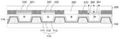
图1为本发明实施方式显示面板的结构示意图;FIG. 1 is a schematic structural diagram of a display panel according to an embodiment of the present invention;
图2为第一种示例性实施方式显示面板的结构示意图;FIG. 2 is a schematic structural diagram of a display panel according to a first exemplary embodiment;
图3为第二种示例性实施方式显示面板的结构示意图;3 is a schematic structural diagram of a display panel according to a second exemplary embodiment;
图4为第三种示例性实施方式显示面板的结构示意图;FIG. 4 is a schematic structural diagram of a display panel according to a third exemplary embodiment;
图5为第一种示例性实施方式显示面板的白光发射光谱图;5 is a white light emission spectrum diagram of the display panel of the first exemplary embodiment;
图6为本发明实施方式显示面板的制备方法流程图。FIG. 6 is a flowchart of a method for manufacturing a display panel according to an embodiment of the present invention.
图中:100、基板;110、发光器件、111、阳极层;112、有机发光材料层;113、阴极层;114、像素界定层;200、封装层;210、遮光层;221、红色滤光层;222、绿色滤光层;230、第一红色量子点层;240、第一绿色量子点层;250、透光层;260、黄光转换层;261、第二红色量子点层;262、第二绿色量子。In the figure: 100, substrate; 110, light-emitting device, 111, anode layer; 112, organic light-emitting material layer; 113, cathode layer; 114, pixel defining layer; 200, encapsulation layer; 210, shading layer; 221, red filter layer; 222, green filter layer; 230, first red quantum dot layer; 240, first green quantum dot layer; 250, light transmission layer; 260, yellow light conversion layer; 261, second red quantum dot layer; 262 , the second green quantum.
具体实施方式Detailed ways
现在将参考附图更全面地描述示例实施方式。然而,示例实施方式能够以多种形式实施,且不应被理解为限于在此阐述的实施方式;相反,提供这些实施方式使得本发明将全面和完整,并将示例实施方式的构思全面地传达给本领域的技术人员。图中相同的附图标记表示相同或类似的结构,因而将省略它们的详细描述。Example embodiments will now be described more fully with reference to the accompanying drawings. Example embodiments, however, can be embodied in various forms and should not be construed as limited to the embodiments set forth herein; rather, these embodiments are provided so that this disclosure will be thorough and complete, and will fully convey the concept of example embodiments to those skilled in the art. The same reference numerals in the drawings denote the same or similar structures, and thus their detailed descriptions will be omitted.
虽然本说明书中使用相对性的用语,例如“上”“下”来描述图标的一个组件对于另一组件的相对关系,但是这些术语用于本说明书中仅出于方便,例如根据附图中所述的示例的方向。能理解的是,如果将图标的装置翻转使其上下颠倒,则所叙述在“上”的组件将会成为在“下”的组件。当某结构在其它结构“上”时,有可能是指某结构一体形成于其它结构上,或指某结构“直接”设置在其它结构上,或指某结构通过另一结构“间接”设置在其它结构上。Although relative terms such as "upper" and "lower" are used in this specification to describe the relative relationship of one component of an icon to another component, these terms are used in this specification only for convenience, such as according to the direction of the example described. It will be appreciated that if the device of the icon is turned upside down, the components described as "on" will become the components on "bottom". When a certain structure is "on" other structures, it may mean that a certain structure is integrally formed on other structures, or that a certain structure is "directly" arranged on other structures, or that a certain structure is "indirectly" arranged on another structure through another structure. other structures.
用语“一个”、“一”、“该”、“所述”和“至少一个”用以表示存在一个或多个要素/组成部分/等;用语“包括”和“具有”用以表示开放式的包括在内的意思并且是指除了列出的要素/组成部分/等之外还可存在另外的要素/组成部分/等。The terms "a", "an", "the", "said" and "at least one" are used to indicate the presence of one or more elements/components/etc; the terms "include" and "have" are used to indicate an open-ended Inclusive means and means that additional elements/components/etc may be present in addition to the listed elements/components/etc.
本发明实施方式中提供了一种基于量子点的显示面板,如图1所示,显示面板包括阵列排布的像素,至少部分像素包括红色子像素R、绿色子像素G、蓝色子像素B和白色子像素W,该显示面板包括相对设置的基板100和封装层200,基板100和封装层200之间设有多个发光器件110,多个发光器件110一一对应地设置于各子像素,发光器件110被配置为朝向封装层200发出蓝光。发光器件110和封装层200之间还设有光转换层,光转换层包括对应于红色子像素的第一红色量子点层230、对应于绿色子像素的第一绿色量子点层240、对应于蓝色子像素的透光层250和对应于白色子像素的黄光转换层260;其中,第一红色量子点层230被配置为将对应子像素的发光器件110发出的蓝光转换为红光,第一绿色量子点层240被配置为将对应子像素的发光器件110发出的蓝光转换为绿光,透光层250被配置为透过对应子像素的发光器件110发出的蓝光,黄光转换层260包括量子点,被配置为将对应子像素的发光器件110发出的部分蓝光转换为黄光,同时透过另一部分蓝光,以使转换的黄光和透过黄光转换层260的蓝光混合为白光。An embodiment of the present invention provides a display panel based on quantum dots. As shown in FIG. 1 , the display panel includes pixels arranged in an array, and at least some of the pixels include red sub-pixels R, green sub-pixels G, and blue sub-pixels B. and the white sub-pixel W, the display panel includes a
本发明以蓝光作为各子像素的背光,第一红色量子点层230的红色量子点,将蓝光转换为红光,以使红色子像素显示红色;第一绿色量子点层240的绿色量子点将蓝光转换为绿光,以使绿色子像素显示绿色;透光层250能够透过蓝光,以使蓝色子像素显示蓝色,黄光转换层260的量子点能够将部分蓝光转换为黄光,还能够透过另一部分蓝光,以使转换的黄光和透过的蓝光混合为白光,使白色子像素显示白色。由此实现了RGBW四色显示,大大提升了色彩丰富程度和显示亮度,可以制作分辨率更高的面板。而且该面板无需在白色子像素上设置蓝光滤光片,提高了蓝色背光的利用率,也简化了制备工艺。The present invention uses blue light as the backlight of each sub-pixel, and the red quantum dots of the first red
下面对本发明实施方式的显示面板进行详细说明:The display panel according to the embodiment of the present invention will be described in detail below:
本发明实施方式中,基板100可以采用玻璃基板、塑胶基板或其他硬质或者可挠式基板等。其中,基板100上可设置驱动二极管和驱动电路(图中未示出),作为驱动背板。封装层200可以为封装盖板,也可以为薄膜封装层,以下以封装盖板为例进行说明。In the embodiment of the present invention, the
基板100上设置有像素界定层114,用于定义各子像素的开口区,每个开口区内设置有一个能发蓝光的发光器件110,为各子像素提供背光。在本示例性实施方式中,发光器件110为蓝色有机电致发光器件110(以下简称蓝色OLED器件),有机电致发光器件110能够自发光,色度好且发光效率高、反应速度快、耗电低,可以提高背光光效。The
具体而言,如图1所示,蓝色OLED器件可以包括阳极层111、蓝色有机发光材料层112、阴极层113等膜层,当然还可以进一步包括空穴传输层、电子传输层、电子注入层、空穴注入层及其他膜层。本申请不对此进行特殊限定。Specifically, as shown in FIG. 1 , the blue OLED device may include an
可以理解的是,发光器件110的设置与传统OLED面板设置相似,区别仅在于传统OLED面板每个像素单元设置红绿蓝三个OLED器件,而本示例性实施方式中每个像素单元设置四个蓝色OLED器件。It can be understood that the arrangement of the
需要说明的是,各子像素的蓝色OLED器件的各功能膜层中,除阳极层外,其余功能膜层均可以通过开放式掩膜版整面形成,以便降低成本。但各子像素的蓝色OLED器件仍然能够通过与阳极连接的薄膜晶体管单独控制控制发光。因此,各发光器件仍然可以看做是多个独立的发光器件。以下描述的蓝色OLED器件均指的是各子像素所对应的独立的发光器件。It should be noted that, in each functional film layer of the blue OLED device of each sub-pixel, except the anode layer, the remaining functional film layers can be formed on the entire surface of the open mask, so as to reduce the cost. However, the blue OLED device of each sub-pixel can still be individually controlled and controlled to emit light through the thin film transistor connected to the anode. Therefore, each light-emitting device can still be regarded as a plurality of independent light-emitting devices. The blue OLED devices described below all refer to independent light-emitting devices corresponding to each sub-pixel.
对于红色子像素而言,蓝色OLED器件发出的蓝光照射在第一红色量子点层230上,第一红色量子点层230中的红色量子点为光致发光量子点材料,能将接收到的蓝光转换为红光,以显示红色。对于绿色子像素而言,蓝色OLED器件发出的蓝光照射在第一绿色量子点层240上,第一绿色量子点层240中的绿色量子点也为光致发光量子点材料,能将接收到的蓝光转换为绿光,以显示绿色。For the red sub-pixel, the blue light emitted by the blue OLED device is irradiated on the first red
由于量子点对蓝光的吸收与量子点的数量直接相关,因此转换效率受到量子点层厚度和层中量子点的浓度影响。理想情况下,量子点层厚度越大或是量子点浓度越高,转换效率越高。但实际上,为了与当前越来越薄的显示需求兼容,量子点层的厚度必须减小到大约6到10微米。而量子点浓度如果过大,量子点可能聚集,导致发光效率降低;同时浓度过大会导致粘度过大,进而影响与喷墨打印设备的兼容性。而且量子点对紫外线有强吸收,量子点浓度越高会影响紫外光固化油墨的固化性能。由于这些厚度和浓度的限制,量子点层难以达到100%的转化率,也就是说,仍然会有一部分蓝光穿过量子点层照射出去。Since the absorption of blue light by quantum dots is directly related to the number of quantum dots, the conversion efficiency is affected by the thickness of the quantum dot layer and the concentration of quantum dots in the layer. Ideally, the larger the quantum dot layer thickness or the higher the quantum dot concentration, the higher the conversion efficiency. But in practice, in order to be compatible with the current demand for thinner and thinner displays, the thickness of the quantum dot layer must be reduced to about 6 to 10 microns. If the concentration of quantum dots is too large, the quantum dots may aggregate, resulting in a decrease in luminous efficiency; at the same time, if the concentration is too large, the viscosity will be too large, which in turn affects the compatibility with inkjet printing equipment. Moreover, quantum dots have strong absorption of ultraviolet rays, and the higher the concentration of quantum dots, the curing performance of UV-curable inks will be affected. Due to these thickness and concentration constraints, it is difficult for the quantum dot layer to achieve 100% conversion, that is, there will still be a portion of blue light irradiated through the quantum dot layer.
因此,本示例性实施方式中,在第一红色量子点层230上增加了红色滤光层221,在第一绿色量子点层240上增加了绿色滤光层222,通过滤光层避免蓝光泄漏,使这两种颜色的子像素出射的光线色域更高。实际上,红色滤光层221和绿色滤光层222均设置于封装盖板上,通过对盒实现发光器件和滤光层的对应。Therefore, in this exemplary embodiment, a
对于蓝色子像素而言,由于蓝色OLED器件发出的本身就是蓝光,因此不需要再设置转换层,而设置为透光层250。需要说明的是,透光层250可以为空气层,也可以为透明材料层。例如可以以透明高分子树脂材料,如亚克力等作为透明材料层,为了进一步提高蓝色子像素的出光效率,可以在透明材料层中增加能够向出光面反射蓝光的反射粒子。For the blue sub-pixel, since the blue OLED device itself emits blue light, there is no need to provide a conversion layer, but the light-transmitting
对于白色子像素而言,蓝色OLED器件发出的蓝光照射在黄光转换层260上,黄光转换层260中的量子点能将接收到的部分蓝光转换为黄光,同时能够透过另一部分蓝光,以使转换的黄光和透过的蓝光混合为白光。具体而言,本实施方式可以以多种方式实现黄光与蓝光的混合。For the white sub-pixels, the blue light emitted by the blue OLED device is irradiated on the yellow
图2所示为第一种示例性实施方式,本实施例中,黄光转换层260包括图中由下至上依次层叠设置的第二红色量子点层261和第二绿色量子点层262,即第二红色量子点层261设于蓝色OLED器件背离基板100的一侧,第二绿色量子点层262设于第二红色量子点层261背离蓝色OLED器件的一侧。FIG. 2 shows the first exemplary embodiment. In this embodiment, the yellow
光线射出过程为:蓝色OLED器件由下至上首先照射在第二红色量子点层261上,由于转化率不会达到100%,第二红色量子点层261能够将部分蓝光转换为红光,同时能够透过另一部分蓝光;第二绿色量子点层262能够将透过第二红色量子点层261的部分蓝光转换为绿光,还能够透过另一部分未被第二红色量子点层261转化的蓝光,同时,由于红光发射光的能量低于绿色量子点激发能量,因此第二绿色量子点层262不会将其转化为绿光,而是使红光透过。最终分别经两个量子点层转换的红光和绿光混合为黄光,黄光和未经两个量子点层转换的蓝光混合为白光由封装层200射出。The light emitting process is as follows: the blue OLED device is first irradiated on the second red
参考图5为本示例性实施方式所示的显示面板白光的发射光谱,可以看出,白光由红光、绿光、蓝光三种颜色光线组成。Referring to the emission spectrum of the white light of the display panel shown in this exemplary embodiment with reference to FIG. 5 , it can be seen that the white light consists of three colors of light: red light, green light, and blue light.
图3所示为第二种示例性实施方式,本实施例中,黄光转换层260包括图中由下至上依次层叠设置的第二绿色量子点层262和第二红色量子点层261,即第二绿色量子点层262设于蓝色OLED器件背离基板100的一侧,第二红色量子点层261设于第二绿色量子点层262背离蓝色OLED器件的一侧。FIG. 3 shows a second exemplary embodiment. In this embodiment, the yellow
光线射出过程为:蓝色OLED器件由下至上首先照射在第二绿色量子点层262上,第二绿色量子点层262能够将部分蓝光转换为绿光,同时能够透过另一部分蓝光。第二红色量子点层261能够将透过第二绿色量子点层262的部分蓝光转换为红光,还能够透过另一部分未被第二绿色量子点层262转化的蓝光,同时,由于绿光发射光的能量高于红色量子点激发能量,因此第二红色量子点层261会将部分绿光转化为红光,当然也会透过另一部分绿光。最终分别经两个量子点层转换的红光和绿光混合为黄光,黄光和未经两个量子点层转换的蓝光混合为白光由封装层200射出。The light emitting process is as follows: the blue OLED device is first irradiated on the second green
第二种示例性实施方式与第一种示例性实施方式相比,由于部分绿光会被第二红色量子点层261转化为红色,因此出射的白光中红光比例较高,而第一种示例性实施方式中红光不会被第二绿色量子点层262转化,因此出射的白光中红光和绿光都有较高的比例。Compared with the first exemplary embodiment, in the second exemplary embodiment, since part of the green light will be converted into red by the second red
以上两种示例性实施方式中,第二红色量子点层261和第二绿色量子点层262的层厚以及层中量子点的浓度都会影响红光或绿光的转化率,从而影响白光中各种颜色光线的比例。因此,需要根据实际产品中对白色色度的要求来调整两个量子点层的层厚以及层中量子点的浓度。In the above two exemplary embodiments, the layer thicknesses of the second red
另外,由于绿色量子点的发射光谱和吸收光谱具有重叠,因此绿光自吸收现象比较明显,其转换率就会较低,从而影响绿光在白光中的占比,降低第二绿色量子点层262的厚度则有利于降低绿光自吸收对白光出光色度的干扰,提高白光出光效果。当然,还可以通过降低第二绿色量子点层262中的量子点浓度来降低绿光自吸收对白光出光色度的干扰,也就是说,第二绿色量子点层262中的绿色量子点浓度小于第一绿色量子点层240中绿色量子点的浓度。需要强调的是,此处所说的降低第二绿色量子点层262的厚度或浓度是指相对于绿色子像素中的第一绿色量子点层240而言,第二绿色量子点层262的厚度和/或浓度小于第一绿色量子点层240。In addition, since the emission spectrum and absorption spectrum of green quantum dots overlap, the self-absorption phenomenon of green light is more obvious, and its conversion rate will be lower, which will affect the proportion of green light in white light and reduce the second green quantum dot layer. The thickness of 262 is beneficial to reduce the interference of green light self-absorption on the white light output chromaticity and improve the white light output effect. Of course, the interference of green light self-absorption on the white light chromaticity can also be reduced by reducing the quantum dot concentration in the second green
而对于红色量子点层而言,由于红色量子点的发射光谱和吸收光谱没有重叠,不存在自吸收现象,因此红色子像素的第一红色量子点层230和白色子像素的第二红色量子点层261厚度或量子点浓度可以相等。For the red quantum dot layer, since the emission spectrum and absorption spectrum of the red quantum dots do not overlap, there is no self-absorption phenomenon, so the first red
图4所示为第三种示例性实施方式,本实施例中,黄光转换层260包括混合的红色量子点和绿色量子点,红色量子点被配置为将蓝色OLED器件发出的部分蓝光转换为红光,同时能够透过另一部分蓝光,绿色量子点被配置为将蓝色OLED器件发出的部分蓝光转换为绿光,同时能够透过另一部分蓝光。同时,由于绿光发射光的能量高于红色量子点激发能量,因此红色量子点会将部分绿光转化为红光,最终分别经混合的两种量子点转换的红光和绿光混合为黄光,黄光和未经量子点转换的蓝光混合为白光由封装层200射出。FIG. 4 shows a third exemplary embodiment. In this embodiment, the yellow
在本示例性实施方式中,由于绿光中的一部分被转换为红光,因此出射的白光中红光比例偏高。由于红色量子点和绿色量子点的浓度会影响红光或绿光的转化率,从而影响白光中各种颜色光线的比例。因此,可以根据实际产品中对白色色度的要求来调整两种量子点的浓度,尽量平衡红光和绿光的比例。In this exemplary embodiment, since a part of green light is converted into red light, the proportion of red light in the outgoing white light is relatively high. Since the concentration of red quantum dots and green quantum dots will affect the conversion rate of red light or green light, it will affect the proportion of light of various colors in white light. Therefore, the concentration of the two quantum dots can be adjusted according to the requirements of the white chromaticity in the actual product, and the ratio of red light and green light can be balanced as much as possible.
同时,本示例性实施方式中,绿色量子点的浓度可以小于第一绿色量子点层240中绿色量子点的浓度,由此可以降低白色子像素中绿光自吸收对白光出光色度的干扰,提高白光出光效果。At the same time, in this exemplary embodiment, the concentration of green quantum dots may be smaller than the concentration of green quantum dots in the first green
第四种示例性实施方式可参考图1,黄光转换层260包括黄色量子点,黄色量子点被配置为将发光器件110发出的部分蓝光转换为黄光,同时透过另一部分蓝光,以使转换的黄光和透过黄光转换层260的蓝光混合为白光。最终经量子点转换的黄光和未经量子点转换的蓝光混合为白光由封装层200射出。For the fourth exemplary embodiment, referring to FIG. 1 , the yellow
在本示例性实施方式中,黄色量子点的浓度会影响黄光的转化率,从而影响白光中各种颜色光线的比例。因此,需要根据实际产品中对白色色度的要求来调整黄色量子点的浓度。In the present exemplary embodiment, the concentration of yellow quantum dots affects the conversion rate of yellow light, thereby affecting the proportion of light of various colors in white light. Therefore, it is necessary to adjust the concentration of yellow quantum dots according to the requirement of white chromaticity in actual products.
在一些示例性实施方式中,封装层可以为封装盖板,由此可以将光转换层形成在封装盖板上,然后通过对盒的方式与基板组成显示面板。In some exemplary embodiments, the encapsulation layer may be an encapsulation cover plate, whereby the light conversion layer may be formed on the encapsulation cover plate, and then a display panel may be formed with the substrate in a box-to-box manner.
参考图1-图4,还可以在封装盖板朝向基板100的一侧设置遮光层(BM)210,遮光层210包括多个遮光部,各遮光部位于相邻两个子像素的滤光层之间,用于防止相邻子像素内量子点层发生光线串扰。Referring to FIGS. 1 to 4 , a light shielding layer (BM) 210 may also be provided on the side of the package cover plate facing the
本申请实施方式还提供上述显示面板的制备方法,参考图6,该方法包括:Embodiments of the present application also provide a method for manufacturing the above-mentioned display panel. Referring to FIG. 6 , the method includes:
步骤S100,提供基板100;Step S100, providing the
步骤S200,在基板100上形成多个发光器件110,多个发光器件110一一对应地设置于各子像素,发光器件110被配置为朝向背离基板100的方向发出蓝光;Step S200, forming a plurality of light-emitting
步骤S300,发光器件110背离基板的一侧形成光转换层,光转换层包括对应于红色子像素的第一红色量子点层230、对应于绿色子像素的第一绿色量子点层240、对应于蓝色子像素的透光层250和对应于白色子像素的黄光转换层260;其中,第一红色量子点层230被配置为将对应子像素的发光器件110发出的蓝光转换为红光,第一绿色量子点层240被配置为将对应子像素的发光器件110发出的蓝光转换为绿光,透光层250被配置为透过对应子像素的发光器件110发出的蓝光,黄光转换层260包括量子点,被配置为将对应子像素的发光器件110发出的部分蓝光转换为黄光,同时透过另一部分蓝光,以使转换的黄光和透过黄光转换层260的蓝光混合为白光;In step S300, a light conversion layer is formed on the side of the
步骤S400,在光转换层背离发光器件110的一侧形成封装层200。In step S400 , the
本实施方式步骤S100中的基板100可以预先形成TFT阵列和驱动电路,以实现对发光器件110的独立控制。The
本实施方式步骤S200中的发光器件110可以采用如旋涂、蒸镀、喷墨打印、磁控溅射等各种方法形成各个膜层。对于实际产品而言,制备好蓝色OLED器件后,在其上方还可以进一步形成平坦化层、封装层等膜层(图中未示出),以对发光器件110进行保护,防止水氧入侵。The light-emitting
本实施方式步骤S300中,可以采用喷墨打印或光刻等工艺形成图案化的量子点层。在一种示例性实施方式中,步骤S400可以采用封装盖板作为封装层,那么可以将光转换层形成在封装盖板上。在形成光转换层之前,先在封装盖板上形成位于相邻子像素之间的遮光层210,然后再形成对应于红色子像素的红色滤光层221和对应于绿色子像素的绿色滤光层222。其次,将第一红色量子点层230形成于红色滤光层221背离封装盖板的一侧,第一绿色量子点层240形成于绿色滤光层222背离封装盖板的一侧。由于第二绿色量子点层262的厚度和/或浓度小于第一绿色量子点层240,因此两个量子点层不能同步形成。但第一红色量子点层230和第二红色量子点层261厚度或量子点浓度可以相等,因此可以同步形成,当然也可以分成两步骤制备。蓝色子像素的透光层250也可以采用喷墨打印或光刻等工艺实现图案化。In step S300 of this embodiment, a process such as inkjet printing or photolithography may be used to form the patterned quantum dot layer. In an exemplary embodiment, in step S400, an encapsulation cover plate may be used as the encapsulation layer, and then the light conversion layer may be formed on the encapsulation cover plate. Before forming the light conversion layer, a
在封装盖板上制备好光转换层后,在光转换层上(图中朝向发光器件110的一面)也可以进一步形成薄膜封装层(图中未示出),以对量子点材料进行保护,防止其氧化。After the light conversion layer is prepared on the packaging cover plate, a thin film packaging layer (not shown in the figure) can also be further formed on the light conversion layer (the side facing the light-emitting
最后将形成有发光器件的基板100和形成有滤光层、遮光层和光转换层的封装盖板对盒,形成完整的显示面板。Finally, the
在其他示例性实施方式中,步骤S400的封装层200也可以为薄膜封装的形式,那么光转换层和滤光层需要形成在各子像素的开口区内,然后通过薄膜封装层对光转换层和滤光层进行保护,以进一步降低显示面板的厚度。光转换层同样可通过喷墨打印或光刻等工艺形成,但该工艺对光转换层的形成难度要求更高。In other exemplary embodiments, the
需要说明的是,上述步骤编号仅是为了描述方便,并不是对步骤顺序的限定,本领域技术人员完全可以根据实际工艺情况调整顺序。It should be noted that the above step numbers are only for the convenience of description and are not intended to limit the sequence of the steps, and those skilled in the art can completely adjust the sequence according to the actual process conditions.
本申请实施方式还提供一种显示装置,该显示装置包括上述实施方式的基于量子点的显示面板。由于该显示装置具有上述显示面板,因此具有相同的有益效果,本申请在此不再赘述。Embodiments of the present application further provide a display device, which includes the quantum dot-based display panel of the above-mentioned embodiments. Since the display device has the above-mentioned display panel, it has the same beneficial effects, which will not be repeated in this application.
本申请对于显示装置的适用不做具体限制,其可以是电视机、笔记本电脑、平板电脑、可穿戴显示设备、手机、车载显示、导航、电子书、数码相框、广告灯箱等任何具有显示功能的产品或部件。This application does not specifically limit the application of the display device, which can be any display device with display function, such as TV, notebook computer, tablet computer, wearable display device, mobile phone, vehicle display, navigation, e-book, digital photo frame, advertising light box, etc. product or component.
本领域技术人员在考虑说明书及实践这里公开的发明后,将容易想到本发明的其它实施方案。本申请旨在涵盖本发明的任何变型、用途或者适应性变化,这些变型、用途或者适应性变化遵循本发明的一般性原理并包括本发明未公开的本技术领域中的公知常识或惯用技术手段。说明书和实施例仅被视为示例性的,本发明的真正范围和精神由所附的权利要求指出。Other embodiments of the invention will readily occur to those skilled in the art upon consideration of the specification and practice of the invention disclosed herein. This application is intended to cover any variations, uses or adaptations of the invention which follow the general principles of the invention and which include common knowledge or conventional techniques in the art not disclosed by the invention . The specification and examples are to be regarded as exemplary only, with the true scope and spirit of the invention being indicated by the appended claims.
Claims (15)
Translated fromChinesePriority Applications (2)
| Application Number | Priority Date | Filing Date | Title |
|---|---|---|---|
| CN202010456483.1ACN111509025A (en) | 2020-05-26 | 2020-05-26 | Quantum dot-based display panel, preparation method thereof, and display device |
| US17/208,033US11637260B2 (en) | 2020-05-26 | 2021-03-22 | Quantum dot-based display panel and method for fabricating the same, and display device |
Applications Claiming Priority (1)
| Application Number | Priority Date | Filing Date | Title |
|---|---|---|---|
| CN202010456483.1ACN111509025A (en) | 2020-05-26 | 2020-05-26 | Quantum dot-based display panel, preparation method thereof, and display device |
Publications (1)
| Publication Number | Publication Date |
|---|---|
| CN111509025Atrue CN111509025A (en) | 2020-08-07 |
Family
ID=71878668
Family Applications (1)
| Application Number | Title | Priority Date | Filing Date |
|---|---|---|---|
| CN202010456483.1APendingCN111509025A (en) | 2020-05-26 | 2020-05-26 | Quantum dot-based display panel, preparation method thereof, and display device |
Country Status (2)
| Country | Link |
|---|---|
| US (1) | US11637260B2 (en) |
| CN (1) | CN111509025A (en) |
Cited By (17)
| Publication number | Priority date | Publication date | Assignee | Title |
|---|---|---|---|---|
| CN112002742A (en)* | 2020-08-12 | 2020-11-27 | 武汉华星光电半导体显示技术有限公司 | OLED display panel and manufacturing method thereof |
| CN112037674A (en)* | 2020-09-22 | 2020-12-04 | 京东方科技集团股份有限公司 | Area light source, manufacturing method thereof and display device |
| CN112164709A (en)* | 2020-09-24 | 2021-01-01 | 武汉华星光电半导体显示技术有限公司 | Organic light emitting diode display panel, preparation method thereof and display device |
| CN112599096A (en)* | 2020-12-31 | 2021-04-02 | 长沙惠科光电有限公司 | Pixel driving structure, pixel driving method and display device |
| CN112635531A (en)* | 2020-12-21 | 2021-04-09 | 深圳扑浪创新科技有限公司 | Quantum dot display device and application thereof |
| CN112635642A (en)* | 2020-12-21 | 2021-04-09 | 深圳扑浪创新科技有限公司 | Display device based on quantum dot electrodeposition and application thereof |
| CN112864333A (en)* | 2021-01-26 | 2021-05-28 | 合肥维信诺科技有限公司 | Display panel and display device |
| CN113066830A (en)* | 2021-03-16 | 2021-07-02 | 京东方科技集团股份有限公司 | A display panel, method for producing the same, and display device |
| CN113270455A (en)* | 2021-04-29 | 2021-08-17 | 合肥维信诺科技有限公司 | Backlight module, display panel and display device |
| CN114035363A (en)* | 2021-11-25 | 2022-02-11 | 深圳市华星光电半导体显示技术有限公司 | Display panel and quantum dot color film substrate |
| CN114597234A (en)* | 2020-12-04 | 2022-06-07 | 中强光电股份有限公司 | display device |
| WO2022134310A1 (en)* | 2020-12-21 | 2022-06-30 | 深圳扑浪创新科技有限公司 | Quantum dot display device and preparation method therefor |
| CN114725177A (en)* | 2022-04-13 | 2022-07-08 | 业成科技(成都)有限公司 | Display panel and electronic device |
| CN115472658A (en)* | 2022-09-19 | 2022-12-13 | 京东方科技集团股份有限公司 | Display panel, manufacturing method thereof, and display device |
| JP2023511637A (en)* | 2020-12-25 | 2023-03-22 | 深▲セン▼▲撲▼浪▲創▼新科技有限公司 | Quantum dot display panel, manufacturing method thereof, and display device |
| WO2023105620A1 (en)* | 2021-12-07 | 2023-06-15 | シャープディスプレイテクノロジー株式会社 | Display device |
| WO2025050933A1 (en)* | 2023-09-04 | 2025-03-13 | 京东方科技集团股份有限公司 | Display panel and preparation method therefor, and display apparatus |
Families Citing this family (7)
| Publication number | Priority date | Publication date | Assignee | Title |
|---|---|---|---|---|
| KR20210017373A (en)* | 2019-08-08 | 2021-02-17 | 엘지디스플레이 주식회사 | Wavelength control film and display device |
| KR102853006B1 (en)* | 2020-06-26 | 2025-08-29 | 엘지디스플레이 주식회사 | Display device |
| US20230309360A1 (en)* | 2020-09-01 | 2023-09-28 | Sharp Kabushiki Kaisha | Light-emitting element and display device |
| CN116264874A (en)* | 2021-09-02 | 2023-06-16 | 京东方科技集团股份有限公司 | Display panel, preparation method thereof and display device |
| KR20230081906A (en)* | 2021-11-30 | 2023-06-08 | 삼성디스플레이 주식회사 | Display panel and electronic device including the same |
| CN114566516B (en)* | 2022-02-28 | 2025-02-07 | 厦门天马微电子有限公司 | Display panel and display device |
| US12237447B2 (en) | 2023-01-13 | 2025-02-25 | Tectus Corporation | Quantum dot layer for color, micro-led displays |
Citations (4)
| Publication number | Priority date | Publication date | Assignee | Title |
|---|---|---|---|---|
| CN105204103A (en)* | 2015-10-09 | 2015-12-30 | 深圳市华星光电技术有限公司 | Quantum-dot color filter and liquid crystal display device |
| CN106918941A (en)* | 2015-11-26 | 2017-07-04 | 三星显示有限公司 | Quantum dot colour filter and the display device including the quantum dot colour filter |
| CN109103344A (en)* | 2018-07-25 | 2018-12-28 | 云谷(固安)科技有限公司 | A kind of white light OLED device and display device |
| CN111048556A (en)* | 2018-10-11 | 2020-04-21 | 三星电子株式会社 | Display panel and display device having the same |
Family Cites Families (7)
| Publication number | Priority date | Publication date | Assignee | Title |
|---|---|---|---|---|
| TWI580031B (en)* | 2013-12-26 | 2017-04-21 | 鴻海精密工業股份有限公司 | Color conversion layer, organic electroluminescence display panel, and liquid crystal display panel |
| CN108962021A (en)* | 2017-05-23 | 2018-12-07 | 群创光电股份有限公司 | Display panel |
| US10403686B2 (en)* | 2017-09-15 | 2019-09-03 | Shenzhen China Star Optoelectronics Semiconductor Display Technology Co., Ltd | Color film substrate and display device |
| US11049439B2 (en)* | 2018-04-19 | 2021-06-29 | Innolux Corporation | Display device, tiling electronic device and method for repairing a display device |
| US10692941B2 (en)* | 2018-07-20 | 2020-06-23 | Shenzhen China Star Optoelectronics Semiconductor Display Technology Co., Ltd. | Organic light emitting diode display |
| KR102589861B1 (en)* | 2018-11-01 | 2023-10-16 | 삼성전자주식회사 | Display device |
| US10923672B1 (en)* | 2019-11-06 | 2021-02-16 | Shenzhen China Star Optoelectronics Semiconductor Display Technology Co., Ltd. | Quantum dot organic light emitting diode display panel |
- 2020
- 2020-05-26CNCN202010456483.1Apatent/CN111509025A/enactivePending
- 2021
- 2021-03-22USUS17/208,033patent/US11637260B2/enactiveActive
Patent Citations (4)
| Publication number | Priority date | Publication date | Assignee | Title |
|---|---|---|---|---|
| CN105204103A (en)* | 2015-10-09 | 2015-12-30 | 深圳市华星光电技术有限公司 | Quantum-dot color filter and liquid crystal display device |
| CN106918941A (en)* | 2015-11-26 | 2017-07-04 | 三星显示有限公司 | Quantum dot colour filter and the display device including the quantum dot colour filter |
| CN109103344A (en)* | 2018-07-25 | 2018-12-28 | 云谷(固安)科技有限公司 | A kind of white light OLED device and display device |
| CN111048556A (en)* | 2018-10-11 | 2020-04-21 | 三星电子株式会社 | Display panel and display device having the same |
Cited By (20)
| Publication number | Priority date | Publication date | Assignee | Title |
|---|---|---|---|---|
| CN112002742A (en)* | 2020-08-12 | 2020-11-27 | 武汉华星光电半导体显示技术有限公司 | OLED display panel and manufacturing method thereof |
| CN112037674A (en)* | 2020-09-22 | 2020-12-04 | 京东方科技集团股份有限公司 | Area light source, manufacturing method thereof and display device |
| CN112164709A (en)* | 2020-09-24 | 2021-01-01 | 武汉华星光电半导体显示技术有限公司 | Organic light emitting diode display panel, preparation method thereof and display device |
| CN114597234A (en)* | 2020-12-04 | 2022-06-07 | 中强光电股份有限公司 | display device |
| CN112635642A (en)* | 2020-12-21 | 2021-04-09 | 深圳扑浪创新科技有限公司 | Display device based on quantum dot electrodeposition and application thereof |
| CN112635531A (en)* | 2020-12-21 | 2021-04-09 | 深圳扑浪创新科技有限公司 | Quantum dot display device and application thereof |
| WO2022134310A1 (en)* | 2020-12-21 | 2022-06-30 | 深圳扑浪创新科技有限公司 | Quantum dot display device and preparation method therefor |
| JP2023511637A (en)* | 2020-12-25 | 2023-03-22 | 深▲セン▼▲撲▼浪▲創▼新科技有限公司 | Quantum dot display panel, manufacturing method thereof, and display device |
| US11971166B2 (en) | 2020-12-25 | 2024-04-30 | Shenzhen Planck Innovation Technology Co., Ltd | Quantum dot display panel, preparation method thereof and display device |
| CN112599096A (en)* | 2020-12-31 | 2021-04-02 | 长沙惠科光电有限公司 | Pixel driving structure, pixel driving method and display device |
| CN112864333A (en)* | 2021-01-26 | 2021-05-28 | 合肥维信诺科技有限公司 | Display panel and display device |
| CN113066830A (en)* | 2021-03-16 | 2021-07-02 | 京东方科技集团股份有限公司 | A display panel, method for producing the same, and display device |
| CN113066830B (en)* | 2021-03-16 | 2022-07-01 | 京东方科技集团股份有限公司 | Display panel, preparation method thereof and display device |
| CN113270455A (en)* | 2021-04-29 | 2021-08-17 | 合肥维信诺科技有限公司 | Backlight module, display panel and display device |
| CN114035363A (en)* | 2021-11-25 | 2022-02-11 | 深圳市华星光电半导体显示技术有限公司 | Display panel and quantum dot color film substrate |
| WO2023105620A1 (en)* | 2021-12-07 | 2023-06-15 | シャープディスプレイテクノロジー株式会社 | Display device |
| CN114725177A (en)* | 2022-04-13 | 2022-07-08 | 业成科技(成都)有限公司 | Display panel and electronic device |
| CN114725177B (en)* | 2022-04-13 | 2024-03-29 | 业成光电(深圳)有限公司 | Display panels and electronic devices |
| CN115472658A (en)* | 2022-09-19 | 2022-12-13 | 京东方科技集团股份有限公司 | Display panel, manufacturing method thereof, and display device |
| WO2025050933A1 (en)* | 2023-09-04 | 2025-03-13 | 京东方科技集团股份有限公司 | Display panel and preparation method therefor, and display apparatus |
Also Published As
| Publication number | Publication date |
|---|---|
| US11637260B2 (en) | 2023-04-25 |
| US20210376272A1 (en) | 2021-12-02 |
Similar Documents
| Publication | Publication Date | Title |
|---|---|---|
| CN111509025A (en) | Quantum dot-based display panel, preparation method thereof, and display device | |
| US11362148B2 (en) | Quantum dot display panel and manufacturing method thereof | |
| US11832495B2 (en) | Display apparatus and manufacturing method therefor | |
| CN111524463A (en) | Display panel, method for making the same, and display device | |
| TW202009580A (en) | Pixel array package structure and display panel | |
| US20230102283A1 (en) | Display panel and display device | |
| US11647660B2 (en) | Color filter substrate and fabricating method thereof | |
| CN107591431A (en) | A kind of color membrane substrates and display device | |
| US12171109B2 (en) | Flexible display panel, flexible display device and method of forming flexible display panel | |
| KR20150078331A (en) | Organic light emitting diode display device | |
| WO2022047852A1 (en) | Display device and manufacturing method therefor | |
| WO2021035957A1 (en) | Quantum dot oled display panel | |
| KR101481673B1 (en) | Organic light emitting display | |
| WO2020001061A1 (en) | Display substrate and manufacturing method therefor, and display device | |
| CN112310143A (en) | Quantum dot micro-LED display device and preparation method thereof | |
| WO2020211155A1 (en) | Double-sided white organic light-emitting diode display device and manufacturing method thereof | |
| CN110518135A (en) | Quantum dot OLED display panel | |
| WO2020177187A1 (en) | Display panel and display module | |
| WO2022205515A1 (en) | Oled display panel and display apparatus | |
| CN110265531A (en) | Micro-led and display panel | |
| CN111430570B (en) | Display panel and method for manufacturing display panel | |
| CN106876432B (en) | A kind of OLED display device and OLED display | |
| KR20160046202A (en) | Organic light emitting diode display | |
| CN115458566B (en) | Display panel, display device, and method for manufacturing display panel | |
| US20240292720A1 (en) | Touch display panel and preparation method thereof, and display apparatus |
Legal Events
| Date | Code | Title | Description |
|---|---|---|---|
| PB01 | Publication | ||
| PB01 | Publication | ||
| SE01 | Entry into force of request for substantive examination | ||
| SE01 | Entry into force of request for substantive examination |