CN111508847A - Preparation method of solar cell containing alkali metal doped copper indium gallium selenide absorption layer and solar cell - Google Patents
Preparation method of solar cell containing alkali metal doped copper indium gallium selenide absorption layer and solar cellDownload PDFInfo
- Publication number
- CN111508847A CN111508847ACN201910096033.3ACN201910096033ACN111508847ACN 111508847 ACN111508847 ACN 111508847ACN 201910096033 ACN201910096033 ACN 201910096033ACN 111508847 ACN111508847 ACN 111508847A
- Authority
- CN
- China
- Prior art keywords
- layer
- alkali metal
- solar cell
- thickness
- forming
- Prior art date
- Legal status (The legal status is an assumption and is not a legal conclusion. Google has not performed a legal analysis and makes no representation as to the accuracy of the status listed.)
- Pending
Links
- KTSFMFGEAAANTF-UHFFFAOYSA-N[Cu].[Se].[Se].[In]Chemical compound[Cu].[Se].[Se].[In]KTSFMFGEAAANTF-UHFFFAOYSA-N0.000titleclaimsabstractdescription91
- 229910052783alkali metalInorganic materials0.000titleclaimsabstractdescription80
- 150000001340alkali metalsChemical class0.000titleclaimsabstractdescription80
- 238000010521absorption reactionMethods0.000titleclaimsabstractdescription53
- 238000002360preparation methodMethods0.000titleclaimsabstractdescription30
- 239000000758substrateSubstances0.000claimsabstractdescription51
- 230000004888barrier functionEffects0.000claimsabstractdescription31
- 238000010549co-EvaporationMethods0.000claimsabstractdescription10
- 238000000137annealingMethods0.000claimsabstractdescription6
- 239000010408filmSubstances0.000claimsdescription61
- XLOMVQKBTHCTTD-UHFFFAOYSA-NZinc monoxideChemical compound[Zn]=OXLOMVQKBTHCTTD-UHFFFAOYSA-N0.000claimsdescription36
- 238000001704evaporationMethods0.000claimsdescription36
- ZOKXTWBITQBERF-UHFFFAOYSA-NMolybdenumChemical compound[Mo]ZOKXTWBITQBERF-UHFFFAOYSA-N0.000claimsdescription35
- 229910052750molybdenumInorganic materials0.000claimsdescription35
- 239000011733molybdenumSubstances0.000claimsdescription35
- 230000008020evaporationEffects0.000claimsdescription34
- 239000006096absorbing agentSubstances0.000claimsdescription31
- 239000010409thin filmSubstances0.000claimsdescription20
- 239000011787zinc oxideSubstances0.000claimsdescription18
- 238000004519manufacturing processMethods0.000claimsdescription14
- 238000004544sputter depositionMethods0.000claimsdescription12
- 229910052701rubidiumInorganic materials0.000claimsdescription11
- 238000007738vacuum evaporationMethods0.000claimsdescription9
- 150000004820halidesChemical class0.000claimsdescription6
- 238000005507sprayingMethods0.000claimsdescription4
- 229910052581Si3N4Inorganic materials0.000claimsdescription3
- 229910052792caesiumInorganic materials0.000claimsdescription2
- 239000000463materialSubstances0.000claimsdescription2
- 229910052700potassiumInorganic materials0.000claimsdescription2
- 238000001771vacuum depositionMethods0.000claimsdescription2
- VYPSYNLAJGMNEJ-UHFFFAOYSA-NSilicium dioxideChemical groupO=[Si]=OVYPSYNLAJGMNEJ-UHFFFAOYSA-N0.000claims2
- PNEYBMLMFCGWSK-UHFFFAOYSA-Naluminium oxideInorganic materials[O-2].[O-2].[O-2].[Al+3].[Al+3]PNEYBMLMFCGWSK-UHFFFAOYSA-N0.000claims1
- 229910052681coesiteInorganic materials0.000claims1
- 229910052593corundumInorganic materials0.000claims1
- 229910052906cristobaliteInorganic materials0.000claims1
- 239000000377silicon dioxideSubstances0.000claims1
- 229910052682stishoviteInorganic materials0.000claims1
- 229910052905tridymiteInorganic materials0.000claims1
- 229910001845yogo sapphireInorganic materials0.000claims1
- 238000006243chemical reactionMethods0.000abstractdescription15
- 230000000694effectsEffects0.000abstractdescription3
- 238000002425crystallisationMethods0.000abstractdescription2
- 230000008025crystallizationEffects0.000abstractdescription2
- 239000010410layerSubstances0.000description236
- 238000000034methodMethods0.000description49
- PUZPDOWCWNUUKD-UHFFFAOYSA-Msodium fluorideChemical compound[F-].[Na+]PUZPDOWCWNUUKD-UHFFFAOYSA-M0.000description36
- 239000011775sodium fluorideSubstances0.000description18
- 235000013024sodium fluorideNutrition0.000description18
- 239000011734sodiumSubstances0.000description11
- 229910052980cadmium sulfideInorganic materials0.000description10
- 229910052708sodiumInorganic materials0.000description9
- 239000010949copperSubstances0.000description7
- 238000001755magnetron sputter depositionMethods0.000description6
- 230000000052comparative effectEffects0.000description5
- 238000012360testing methodMethods0.000description5
- 238000009826distributionMethods0.000description4
- 229920001721polyimidePolymers0.000description4
- 239000005361soda-lime glassSubstances0.000description4
- 239000002344surface layerSubstances0.000description4
- 229910018072Al 2 O 3Inorganic materials0.000description3
- 239000000203mixtureSubstances0.000description3
- 229910052711seleniumInorganic materials0.000description3
- CPELXLSAUQHCOX-UHFFFAOYSA-MBromideChemical compound[Br-]CPELXLSAUQHCOX-UHFFFAOYSA-M0.000description2
- VEXZGXHMUGYJMC-UHFFFAOYSA-MChloride anionChemical compound[Cl-]VEXZGXHMUGYJMC-UHFFFAOYSA-M0.000description2
- KRHYYFGTRYWZRS-UHFFFAOYSA-MFluoride anionChemical compound[F-]KRHYYFGTRYWZRS-UHFFFAOYSA-M0.000description2
- 239000004642PolyimideSubstances0.000description2
- 229910004298SiO 2Inorganic materials0.000description2
- 238000005229chemical vapour depositionMethods0.000description2
- 238000004140cleaningMethods0.000description2
- 239000002131composite materialSubstances0.000description2
- 229910052802copperInorganic materials0.000description2
- 229910052733galliumInorganic materials0.000description2
- XMBWDFGMSWQBCA-UHFFFAOYSA-Nhydrogen iodideChemical compoundIXMBWDFGMSWQBCA-UHFFFAOYSA-N0.000description2
- 229910052738indiumInorganic materials0.000description2
- 238000012986modificationMethods0.000description2
- 230000004048modificationEffects0.000description2
- 238000005240physical vapour depositionMethods0.000description2
- 239000002994raw materialSubstances0.000description2
- WUPHOULIZUERAE-UHFFFAOYSA-N3-(oxolan-2-yl)propanoic acidChemical compoundOC(=O)CCC1CCCO1WUPHOULIZUERAE-UHFFFAOYSA-N0.000description1
- VHUUQVKOLVNVRT-UHFFFAOYSA-NAmmonium hydroxideChemical compound[NH4+].[OH-]VHUUQVKOLVNVRT-UHFFFAOYSA-N0.000description1
- RYGMFSIKBFXOCR-UHFFFAOYSA-NCopperChemical compound[Cu]RYGMFSIKBFXOCR-UHFFFAOYSA-N0.000description1
- -1Si 3 N 4Inorganic materials0.000description1
- CDBYLPFSWZWCQE-UHFFFAOYSA-LSodium CarbonateChemical compound[Na+].[Na+].[O-]C([O-])=OCDBYLPFSWZWCQE-UHFFFAOYSA-L0.000description1
- HCHKCACWOHOZIP-UHFFFAOYSA-NZincChemical compound[Zn]HCHKCACWOHOZIP-UHFFFAOYSA-N0.000description1
- PMUIBVMKQVKHBE-UHFFFAOYSA-N[S].NC(N)=OChemical compound[S].NC(N)=OPMUIBVMKQVKHBE-UHFFFAOYSA-N0.000description1
- 239000003513alkaliSubstances0.000description1
- 229910052782aluminiumInorganic materials0.000description1
- XAGFODPZIPBFFR-UHFFFAOYSA-NaluminiumChemical compound[Al]XAGFODPZIPBFFR-UHFFFAOYSA-N0.000description1
- 235000011114ammonium hydroxideNutrition0.000description1
- 238000004458analytical methodMethods0.000description1
- 230000015572biosynthetic processEffects0.000description1
- LHQLJMJLROMYRN-UHFFFAOYSA-Lcadmium acetateChemical compound[Cd+2].CC([O-])=O.CC([O-])=OLHQLJMJLROMYRN-UHFFFAOYSA-L0.000description1
- 239000000919ceramicSubstances0.000description1
- 229910021419crystalline siliconInorganic materials0.000description1
- 238000005137deposition processMethods0.000description1
- 238000011161developmentMethods0.000description1
- 238000010586diagramMethods0.000description1
- 238000005516engineering processMethods0.000description1
- 239000011521glassSubstances0.000description1
- 238000009776industrial productionMethods0.000description1
- 229910052751metalInorganic materials0.000description1
- 239000002184metalSubstances0.000description1
- 239000002923metal particleSubstances0.000description1
- 238000001000micrographMethods0.000description1
- 230000000877morphologic effectEffects0.000description1
- 238000005457optimizationMethods0.000description1
- 238000011056performance testMethods0.000description1
- 238000011160researchMethods0.000description1
- 238000013341scale-upMethods0.000description1
- 238000001004secondary ion mass spectrometryMethods0.000description1
- HQVNEWCFYHHQES-UHFFFAOYSA-Nsilicon nitrideChemical compoundN12[Si]34N5[Si]62N3[Si]51N64HQVNEWCFYHHQES-UHFFFAOYSA-N0.000description1
- 238000004611spectroscopical analysisMethods0.000description1
- 229910001220stainless steelInorganic materials0.000description1
- 239000010935stainless steelSubstances0.000description1
- 239000000126substanceSubstances0.000description1
- 239000013077target materialSubstances0.000description1
- XLYOFNOQVPJJNP-UHFFFAOYSA-NwaterSubstancesOXLYOFNOQVPJJNP-UHFFFAOYSA-N0.000description1
- 238000004876x-ray fluorescenceMethods0.000description1
- 229910052725zincInorganic materials0.000description1
- 239000011701zincSubstances0.000description1
Images

Classifications
- H—ELECTRICITY
- H10—SEMICONDUCTOR DEVICES; ELECTRIC SOLID-STATE DEVICES NOT OTHERWISE PROVIDED FOR
- H10F—INORGANIC SEMICONDUCTOR DEVICES SENSITIVE TO INFRARED RADIATION, LIGHT, ELECTROMAGNETIC RADIATION OF SHORTER WAVELENGTH OR CORPUSCULAR RADIATION
- H10F77/00—Constructional details of devices covered by this subclass
- H10F77/10—Semiconductor bodies
- H10F77/12—Active materials
- H10F77/126—Active materials comprising only Group I-III-VI chalcopyrite materials, e.g. CuInSe2, CuGaSe2 or CuInGaSe2 [CIGS]
- H10F77/1265—Active materials comprising only Group I-III-VI chalcopyrite materials, e.g. CuInSe2, CuGaSe2 or CuInGaSe2 [CIGS] characterised by the dopants
- H—ELECTRICITY
- H01—ELECTRIC ELEMENTS
- H01L—SEMICONDUCTOR DEVICES NOT COVERED BY CLASS H10
- H01L21/00—Processes or apparatus adapted for the manufacture or treatment of semiconductor or solid state devices or of parts thereof
- H01L21/02—Manufacture or treatment of semiconductor devices or of parts thereof
- H01L21/04—Manufacture or treatment of semiconductor devices or of parts thereof the devices having potential barriers, e.g. a PN junction, depletion layer or carrier concentration layer
- H01L21/34—Manufacture or treatment of semiconductor devices or of parts thereof the devices having potential barriers, e.g. a PN junction, depletion layer or carrier concentration layer the devices having semiconductor bodies not provided for in groups H01L21/18, H10D48/04 and H10D48/07, with or without impurities, e.g. doping materials
- H01L21/38—Diffusion of impurity materials, e.g. doping materials, electrode materials, into or out of a semiconductor body, or between semiconductor regions
- H01L21/385—Diffusion of impurity materials, e.g. doping materials, electrode materials, into or out of a semiconductor body, or between semiconductor regions using diffusion into or out of a solid from or into a solid phase, e.g. a doped oxide layer
- H—ELECTRICITY
- H10—SEMICONDUCTOR DEVICES; ELECTRIC SOLID-STATE DEVICES NOT OTHERWISE PROVIDED FOR
- H10F—INORGANIC SEMICONDUCTOR DEVICES SENSITIVE TO INFRARED RADIATION, LIGHT, ELECTROMAGNETIC RADIATION OF SHORTER WAVELENGTH OR CORPUSCULAR RADIATION
- H10F71/00—Manufacture or treatment of devices covered by this subclass
- Y—GENERAL TAGGING OF NEW TECHNOLOGICAL DEVELOPMENTS; GENERAL TAGGING OF CROSS-SECTIONAL TECHNOLOGIES SPANNING OVER SEVERAL SECTIONS OF THE IPC; TECHNICAL SUBJECTS COVERED BY FORMER USPC CROSS-REFERENCE ART COLLECTIONS [XRACs] AND DIGESTS
- Y02—TECHNOLOGIES OR APPLICATIONS FOR MITIGATION OR ADAPTATION AGAINST CLIMATE CHANGE
- Y02E—REDUCTION OF GREENHOUSE GAS [GHG] EMISSIONS, RELATED TO ENERGY GENERATION, TRANSMISSION OR DISTRIBUTION
- Y02E10/00—Energy generation through renewable energy sources
- Y02E10/50—Photovoltaic [PV] energy
- Y02E10/541—CuInSe2 material PV cells
- Y—GENERAL TAGGING OF NEW TECHNOLOGICAL DEVELOPMENTS; GENERAL TAGGING OF CROSS-SECTIONAL TECHNOLOGIES SPANNING OVER SEVERAL SECTIONS OF THE IPC; TECHNICAL SUBJECTS COVERED BY FORMER USPC CROSS-REFERENCE ART COLLECTIONS [XRACs] AND DIGESTS
- Y02—TECHNOLOGIES OR APPLICATIONS FOR MITIGATION OR ADAPTATION AGAINST CLIMATE CHANGE
- Y02P—CLIMATE CHANGE MITIGATION TECHNOLOGIES IN THE PRODUCTION OR PROCESSING OF GOODS
- Y02P70/00—Climate change mitigation technologies in the production process for final industrial or consumer products
- Y02P70/50—Manufacturing or production processes characterised by the final manufactured product
Landscapes
- Engineering & Computer Science (AREA)
- Physics & Mathematics (AREA)
- Condensed Matter Physics & Semiconductors (AREA)
- General Physics & Mathematics (AREA)
- Manufacturing & Machinery (AREA)
- Computer Hardware Design (AREA)
- Microelectronics & Electronic Packaging (AREA)
- Power Engineering (AREA)
- Photovoltaic Devices (AREA)
Abstract
Description
Translated fromChinese技术领域technical field
本发明涉及铜铟镓硒太阳能电池的制备方法领域,具体涉及一种含有碱金属掺杂铜铟镓硒吸收层的太阳能电池的制备方法及太阳能电池。The invention relates to the field of preparation methods of copper indium gallium selenide solar cells, in particular to a preparation method and solar cell of a solar cell containing an alkali metal-doped copper indium gallium selenide absorption layer.
背景技术Background technique
目前制约铜铟镓硒(CIGS)薄膜光伏电池产业发展的一个很重要的因素就是CIGS薄膜光伏组件的转换效率偏低,低于市场上主流的晶硅组件的转换效率。提升工业生产的CIGS薄膜光伏组件的转换效率,除了改良光伏组件制造过程中的各个工艺环节外,最核心、最根本的还是要提高CIGS吸收层的性能,即CIGS薄膜电池本身的转换效率。At present, a very important factor restricting the development of copper indium gallium selenide (CIGS) thin film photovoltaic cell industry is the low conversion efficiency of CIGS thin film photovoltaic modules, which is lower than the conversion efficiency of mainstream crystalline silicon modules in the market. To improve the conversion efficiency of industrially produced CIGS thin-film photovoltaic modules, in addition to improving various process links in the photovoltaic module manufacturing process, the core and most fundamental thing is to improve the performance of the CIGS absorber layer, that is, the conversion efficiency of the CIGS thin-film cell itself.
目前铜铟镓硒太阳能电池常用的制备方法包括一步法和三步法。一步法是吸收层的四种元同时蒸发,在薄膜沉积过程中,保持铜铟镓硒四个蒸发源的流量不变,这种工艺适合大面积生产,但是制得的CIGS薄膜晶粒尺寸小,不能形成具有梯度带隙的结构。三步共蒸发工艺包括:第一步,在基底上蒸发In、Ga、Se形成一层(In0.7Ga0.3)2Se3预置层;第二步,在基底上蒸发Cu、Se,促进晶粒生长,使得薄膜富铜;第三步,保持第二步的基底温度,蒸发In、Ga、Se,经过三步法工艺制备的薄膜表面光滑、晶粒大、紧凑,且存在Ga的双梯度带隙。At present, the commonly used preparation methods of copper indium gallium selenide solar cells include one-step method and three-step method. The one-step method is that the four elements of the absorption layer are evaporated at the same time. During the film deposition process, the flow rates of the four evaporation sources of copper indium gallium selenide are kept unchanged. This process is suitable for large-area production, but the obtained CIGS film has a small grain size. , cannot form a structure with a gradient band gap. The three-step co-evaporation process includes: the first step, evaporating In, Ga and Se on the substrate to form a pre-layer of (In0.7 Ga0.3 )2 Se3 ; the second step, evaporating Cu and Se on the substrate to promote the crystallinity Grain growth makes the film rich in copper; in the third step, the substrate temperature of the second step is maintained, and In, Ga, and Se are evaporated. The film prepared by the three-step process has a smooth surface, large and compact grains, and there is a double gradient of Ga. Bandgap.
考虑装备和工艺放大难度、生产成本和产品良率等因素,工业生产的CIGS薄膜电池一般不得不采用共蒸发一步法方法制备CIGS吸收层,但其转换效率与实验室采用共蒸发三步法制备的CIGS效率之间存在较大的差距。Considering factors such as equipment and process scale-up difficulty, production cost and product yield, industrially produced CIGS thin-film cells generally have to use a one-step co-evaporation method to prepare the CIGS absorber layer, but its conversion efficiency is comparable to that of the laboratory using a three-step co-evaporation method There is a large gap between the CIGS efficiencies.
为了提升适用于工业生产的一步法CIGS薄膜光伏组件的转换效率,一些研究在CIGS吸收层的制备过程中加入碱金属处理过程。In order to improve the conversion efficiency of one-step CIGS thin-film photovoltaic modules suitable for industrial production, some studies have added an alkali metal treatment process during the preparation of the CIGS absorber layer.
CN104425649A公开了一步法吸收层后掺钠柔性太阳电池的制备方法,该制备方法包括:首先制备聚酰亚胺膜-苏打玻璃构成的刚性复合衬底,之后在复合衬底上依次制备Mo背接触层、铜铟镓硒吸收层、氟化钠预置层、硫化镉缓冲层、透明窗口层和上电极。CN104425649A discloses a preparation method of a sodium-doped flexible solar cell after a one-step absorption layer. The preparation method includes: firstly preparing a rigid composite substrate composed of polyimide film and soda glass, and then sequentially preparing Mo back contacts on the composite substrate layer, copper indium gallium selenide absorber layer, sodium fluoride pre-position layer, cadmium sulfide buffer layer, transparent window layer and upper electrode.
CN106816490A公开了一种碱金属元素掺杂的铜铟镓硒吸收层薄膜的制备方法,该制备方法包括:预先在钠钙玻璃衬底上制作氮化硅阻挡层;之后在衬底上沉积掺有碱金属元素的背接触Mo层和CIG金属预制层。CN106816490A discloses a preparation method of an alkali metal element-doped copper indium gallium selenide absorber film. The preparation method includes: pre-forming a silicon nitride barrier layer on a soda-lime glass substrate; The back of the alkali metal element contacts the Mo layer and the CIG metal prefab.
三步法制备的CIGS吸收层,能控制吸收层中Ga在梯度方向的分布,使Ga的含量在吸收层中呈V型分布,从而优化吸收层中的带隙结构,因此效率较一步法相对较高。并且三步法形成的这种成分和带隙的结构可采用碱金属处理技术进行表面处理,从而能够进一步提升电池效率。由于三步法和一步法所制得的CIGS吸收层的带隙结构在梯度方向分布不同,一步法不能精确调控吸收层中的梯度方向的成分和带隙分布,梯度方向的成分和带隙分布很难采用碱金属进行表面优化处理,效率相对较低。The CIGS absorber layer prepared by the three-step method can control the distribution of Ga in the gradient direction in the absorber layer, so that the content of Ga in the absorber layer is V-shaped distribution, so as to optimize the band gap structure in the absorber layer, so the efficiency is relatively higher than that of the one-step method. higher. And the composition and bandgap structure formed by the three-step method can be surface-treated by alkali metal treatment technology, which can further improve the battery efficiency. Because the band gap structure of the CIGS absorber layer prepared by the three-step method and the one-step method is different in the gradient direction, the one-step method cannot accurately control the gradient direction composition and band gap distribution in the absorber layer, and the gradient direction composition and band gap distribution. Surface optimization with alkali metals is difficult and relatively inefficient.
发明内容SUMMARY OF THE INVENTION
本发明的目的是为了克服现有技术存在的含有一步法制得CIGS吸收层的太阳能电池转化效率低、太阳能电池的一致性较差的问题,提供一种含有碱金属掺杂铜铟镓硒吸收层的太阳能电池的制备方法及太阳能电池,该制备方法具有提高太阳能电池的转化效率、提高铜铟镓硒吸收层的结晶效果,且制得的太阳能电池的一致性较好。The purpose of the present invention is to provide a kind of absorption layer containing alkali metal doped copper indium gallium selenide in order to overcome the problems of low conversion efficiency and poor consistency of the solar cell containing the CIGS absorption layer obtained by the one-step method in the prior art. The solar cell preparation method and the solar cell are provided. The preparation method has the advantages of improving the conversion efficiency of the solar cell, improving the crystallization effect of the copper indium gallium selenide absorption layer, and the prepared solar cell has good consistency.
为了实现上述目的,本发明第一方面提供一种含有碱金属掺杂铜铟镓硒吸收层的太阳能电池的制备方法,其中,该制备方法包括如下步骤:In order to achieve the above object, a first aspect of the present invention provides a method for preparing a solar cell containing an alkali metal doped copper indium gallium selenide absorber layer, wherein the preparation method includes the following steps:
(1)在衬底上形成阻挡层;(1) forming a barrier layer on the substrate;
(2)在阻挡层的表面形成背电极层;(2) forming a back electrode layer on the surface of the barrier layer;
(3)在背电极层表面形成第一碱金属层;(3) forming a first alkali metal layer on the surface of the back electrode layer;
(4)在第一碱金属层表面通过一步法共蒸发形成CIGS吸收层;(4) a CIGS absorption layer is formed on the surface of the first alkali metal layer by one-step co-evaporation;
(5)在CIGS吸收层表面形成第二碱金属层;(5) forming a second alkali metal layer on the surface of the CIGS absorption layer;
(6)将步骤(1)-(5)形成的膜层在350-450℃进行退火5-30min。(6) The films formed in steps (1)-(5) are annealed at 350-450° C. for 5-30 minutes.
本发明第二方面提供一种太阳能电池,采用上述的制备方法制得。A second aspect of the present invention provides a solar cell, which is prepared by the above-mentioned preparation method.
通过上述技术方案,本发明采用一步法制备CIGS吸收层,并同时在CIGS吸收层的上表面和下表面均引入碱金属,并经过退火之后,在CIGS层的表面和内部均掺杂有碱金属,采用该方法能够有效提高铜铟镓硒太阳能电池的转换效率,并且制得的铜铟镓硒太阳能电池的稳定性和一致性较佳。Through the above technical scheme, the present invention adopts a one-step method to prepare the CIGS absorption layer, and simultaneously introduces alkali metal on the upper surface and the lower surface of the CIGS absorption layer, and after annealing, the surface and the interior of the CIGS layer are doped with alkali metal The method can effectively improve the conversion efficiency of the copper indium gallium selenide solar cell, and the obtained copper indium gallium selenide solar cell has better stability and consistency.
附图说明Description of drawings
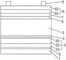
图1是实施例1中太阳能电池的结构示意图;1 is a schematic structural diagram of a solar cell in Example 1;
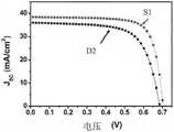
图2是实施例1和对比例2制得的太阳能电池的电压-Jsc曲线;Figure 2 is the voltage-Jsc curve of the solar cells prepared in Example 1 and Comparative Example 2;
图3是实施例1制得的CIGS吸收层的SEM电镜图。FIG. 3 is a SEM electron microscope image of the CIGS absorber layer prepared in Example 1. FIG.
附图标记说明Description of reference numerals
1、衬底 2、阻挡层 3、背电极层 31、第一层钼薄膜1.
32、第二层钼薄膜 33、第三层钼薄膜 4、NaF膜层 5、CIGS吸收层32. The second layer of
6、RbF膜层 7、缓冲层 8、窗口层 81、本征氧化锌层6.
82、铝掺杂氧化锌 9、上电极82. Aluminum doped
层Floor
具体实施方式Detailed ways
在本文中所披露的范围的端点和任何值都不限于该精确的范围或值,这些范围或值应当理解为包含接近这些范围或值的值。对于数值范围来说,各个范围的端点值之间、各个范围的端点值和单独的点值之间,以及单独的点值之间可以彼此组合而得到一个或多个新的数值范围,这些数值范围应被视为在本文中具体公开。The endpoints of ranges and any values disclosed herein are not limited to the precise ranges or values, which are to be understood to encompass values proximate to those ranges or values. For ranges of values, the endpoints of each range, the endpoints of each range and the individual point values, and the individual point values can be combined with each other to yield one or more new ranges of values that Ranges should be considered as specifically disclosed herein.
本发明第一方面提供一种一步法铜铟镓硒吸收层掺杂碱金属的制备方法,其中,该制备方法包括如下步骤:A first aspect of the present invention provides a one-step method for preparing a copper indium gallium selenide absorption layer doped with alkali metal, wherein the preparation method includes the following steps:
(1)在衬底上形成阻挡层;(1) forming a barrier layer on the substrate;
(2)在阻挡层的表面形成背电极层;(2) forming a back electrode layer on the surface of the barrier layer;
(3)在背电极层表面形成第一碱金属层;(3) forming a first alkali metal layer on the surface of the back electrode layer;
(4)在第一碱金属层表面通过一步法共蒸发形成CIGS吸收层;(4) a CIGS absorption layer is formed on the surface of the first alkali metal layer by one-step co-evaporation;
(5)在CIGS吸收层表面形成第二碱金属层;(5) forming a second alkali metal layer on the surface of the CIGS absorption layer;
(6)将步骤(1)-(5)形成的膜层在350-450℃进行退火5-30min。(6) The films formed in steps (1)-(5) are annealed at 350-450° C. for 5-30 minutes.
本发明中的CIGS吸收层采用一步法制得,本发明的发明人经过大量研究发现,在制备铜铟镓硒太阳能电池时,在衬底上依次形成阻挡层、背电极层、第一碱金属层、CIGS吸收层和第二碱金属层,并对上述形成的薄膜进行退火处理,使得采用一步法制得的CIGS吸收层的表面和内部均分布有碱金属。经过上述方法处理后,将该一步法制得的CIGS吸收层用于太阳能电池,能够明显提高太阳能电池的转化效率,并且在工业应用中太阳能电池的一致性较好。The CIGS absorption layer in the present invention is prepared by a one-step method. The inventors of the present invention have found through extensive research that when preparing a copper indium gallium selenide solar cell, a barrier layer, a back electrode layer and a first alkali metal layer are sequentially formed on the substrate. , a CIGS absorbing layer and a second alkali metal layer, and annealing the above-formed thin film, so that the surface and the interior of the CIGS absorbing layer prepared by the one-step method are distributed with alkali metals. After the treatment by the above method, the CIGS absorption layer prepared by the one-step method is used in a solar cell, which can significantly improve the conversion efficiency of the solar cell, and the solar cell has good consistency in industrial applications.
根据本发明,步骤(1)中,衬底的材质没有特别的限定,优选为钠钙玻璃、不锈钢金属、聚酰亚胺中的至少一种。According to the present invention, in step (1), the material of the substrate is not particularly limited, and is preferably at least one of soda lime glass, stainless steel, and polyimide.
阻挡层的制备方法没有特别的限定,例如可以是现有技术中的物理气相沉积或者化学气相沉积的方法,优选采用磁控溅射。所述磁控溅射的条件没有特别的限定,只要能够在衬底上形成材质为SiO2、Si3N4、Al2O3和AlN中的至少一种阻挡层即可,所述阻挡层的厚度为10-50nm,优选为40-50nm。The preparation method of the barrier layer is not particularly limited, for example, it may be the method of physical vapor deposition or chemical vapor deposition in the prior art, preferably magnetron sputtering. The conditions of the magnetron sputtering are not particularly limited, as long as at least one barrier layer made of SiO2 , Si3 N4 , Al2 O3 and AlN can be formed on the substrate, the barrier layer The thickness is 10-50nm, preferably 40-50nm.
根据本发明,步骤(2)中,背电极层的制备方法没有特别的限定,例如可以是现有技术中的物理气相沉积或者化学气相沉积的方法,优选采用直流磁控溅射。所述直流磁控溅射的条件没有特别的限定,只要能够在阻挡层上形成材质为钼的背电极层即可。According to the present invention, in step (2), the preparation method of the back electrode layer is not particularly limited, for example, it can be the method of physical vapor deposition or chemical vapor deposition in the prior art, preferably DC magnetron sputtering. The conditions of the DC magnetron sputtering are not particularly limited, as long as a back electrode layer made of molybdenum can be formed on the barrier layer.
优选地,所述背电极层的厚度为400-1000nm,优选为400-985nm,所述背电极层由一层钼层构成或者由多层钼层叠加构成。更优选地,所述背电极层由三层钼层叠加构成。Preferably, the thickness of the back electrode layer is 400-1000 nm, preferably 400-985 nm, and the back electrode layer is composed of a molybdenum layer or a stack of multiple molybdenum layers. More preferably, the back electrode layer is formed by stacking three molybdenum layers.
若所述背电极层由一层钼层构成,改变直流磁控溅射的时间,使得该钼层的厚度为400-1000nm即可。若所述背电极层由多层钼层叠加构成,通过改变直流磁控溅射的时间和工作气压,使得多层钼层叠加的厚度为400-1000nm即可。优选地,步骤(2)中,形成所述背电极层的溅射条件包括:真空度为(1-3)×10-4Pa,工作气压为0.1-1Pa,衬底温度为25-50℃,射频功率为150-2000W,优选150-600W,工作气体流量为30-50sccm。If the back electrode layer is composed of a molybdenum layer, the time of DC magnetron sputtering can be changed so that the thickness of the molybdenum layer is 400-1000 nm. If the back electrode layer is formed by stacking multiple molybdenum layers, the thickness of the stacking of the multiple molybdenum layers can be 400-1000 nm by changing the time and working pressure of DC magnetron sputtering. Preferably, in step (2), the sputtering conditions for forming the back electrode layer include: a vacuum degree of (1-3)×10-4 Pa, a working pressure of 0.1-1 Pa, and a substrate temperature of 25-50° C. , the radio frequency power is 150-2000W, preferably 150-600W, and the working gas flow is 30-50sccm.
在优选情况下,本发明中的背电极层采用多层钼层叠加,能够进一步提高背电极层与阻挡层以及第一碱金属层的界面接触效果,降低界面接触电阻,提高太阳能电池的结构稳定性。In a preferred case, the back electrode layer in the present invention is stacked with multiple molybdenum layers, which can further improve the interface contact effect between the back electrode layer, the barrier layer and the first alkali metal layer, reduce the interface contact resistance, and improve the structural stability of the solar cell. sex.
根据本发明,步骤(3)中,第一碱金属层的形成方式没有特别的限定,优选采用真空蒸发、真空溅射、溶胶凝胶和纳米喷涂中的至少一种方法形成,更优选采用真空蒸发的方法形成。According to the present invention, in step (3), the formation method of the first alkali metal layer is not particularly limited, and it is preferably formed by at least one of vacuum evaporation, vacuum sputtering, sol-gel and nano-spraying, and more preferably vacuum is used. formed by evaporation.
优选地,形成所述第一碱金属层的真空蒸发的条件包括:蒸发源为含Li和/或Na的卤化物,真空度至少为8×10-4Pa,衬底温度为200-300℃,蒸发源的温度为400-700℃;所述卤化物可以为氟化物、氯化物、溴化物和碘化物中的至少一种。Preferably, the vacuum evaporation conditions for forming the first alkali metal layer include: the evaporation source is a halide containing Li and/or Na, the vacuum degree is at least 8×10⁻⁴ Pa, and the substrate temperature is 200-300°C , the temperature of the evaporation source is 400-700°C; the halide can be at least one of fluoride, chloride, bromide and iodide.
优选地,所述第一碱金属层的厚度为10-40nm。Preferably, the thickness of the first alkali metal layer is 10-40 nm.
根据本发明,步骤(4)中,CIGS吸收层优选采用一步法共蒸发的方法制得,优选地,所述一步法共蒸发的条件包括:衬底的温度为450-580℃,蒸发源温度为250-1300℃,蒸发时间为25-30min。以原子百分含量计,所述CIGS吸收层中的Cu含量为18-25at%、In含量为14-23at%、Ga含量为6.5-9.5at%、Se含量为48-52at%。其中,CIGS吸收层中的各组分的含量均为未掺杂碱金属时通过X射线荧光光谱分析测得。优选地,Cu蒸发源的温度为1100-1300℃,In蒸发源的温度为800-900℃,Ga蒸发源的温度为900-1000℃,Se蒸发源的温度为300-400℃。According to the present invention, in step (4), the CIGS absorption layer is preferably prepared by a one-step co-evaporation method. Preferably, the conditions for the one-step co-evaporation include: the temperature of the substrate is 450-580° C. It is 250-1300℃, and the evaporation time is 25-30min. In terms of atomic percentage, the content of Cu in the CIGS absorption layer is 18-25 at%, the content of In is 14-23 at%, the content of Ga is 6.5-9.5 at%, and the content of Se is 48-52 at%. Wherein, the content of each component in the CIGS absorption layer is measured by X-ray fluorescence spectroscopic analysis when the alkali metal is not doped. Preferably, the temperature of the Cu evaporation source is 1100-1300°C, the temperature of the In evaporation source is 800-900°C, the temperature of the Ga evaporation source is 900-1000°C, and the temperature of the Se evaporation source is 300-400°C.
优选地,步骤(4)中CIGS吸收层的厚度为1.5-3μm。Preferably, the thickness of the CIGS absorption layer in step (4) is 1.5-3 μm.
根据本发明,步骤(5)中,第二碱金属层的制备方法没有特别的限定,优选采用真空蒸发、真空溅射、溶胶凝胶和纳米喷涂中的至少一种方法形成,更优选采用真空蒸发的方法形成。According to the present invention, in step (5), the preparation method of the second alkali metal layer is not particularly limited, it is preferably formed by at least one of vacuum evaporation, vacuum sputtering, sol-gel and nano-spraying, and more preferably vacuum is used. formed by evaporation.
优选地,形成所述第二碱金属层的真空蒸发的条件包括:蒸发源为含K、Rb和Cs中的至少一种的卤化物,真空度至少为8×10⁻⁴Pa,衬底温度为200-300℃,蒸发源的温度为400-700℃;优选地,所述卤化物为氟化物、氯化物、溴化物和碘化物中的至少一种。Preferably, the vacuum evaporation conditions for forming the second alkali metal layer include: the evaporation source is a halide containing at least one of K, Rb and Cs, the vacuum degree is at least 8×10⁻⁴ Pa, the substrate temperature is 200-300°C, and the temperature of the evaporation source is 400-700°C; preferably, the halide is at least one of fluoride, chloride, bromide and iodide.
优选地,所述第二碱金属层的厚度为10-40nm。Preferably, the thickness of the second alkali metal layer is 10-40 nm.
根据本发明,在衬底上依次形成阻挡层、背电极层、第一碱金属层、CIGS层和第二碱金属层,之后将上述形成的膜层在高温(350-450℃)下进行退火处理。采用上述工艺互相配合,使得CIGS吸收层的表面和内部均掺杂有碱金属,能够有效改善一步法制得的CIGS吸收层的结晶质量,提高太阳能电池的转化效率。According to the present invention, a barrier layer, a back electrode layer, a first alkali metal layer, a CIGS layer and a second alkali metal layer are sequentially formed on the substrate, and then the film layers formed above are annealed at high temperature (350-450° C.). deal with. The above-mentioned processes cooperate with each other, so that the surface and the interior of the CIGS absorption layer are doped with alkali metals, which can effectively improve the crystalline quality of the CIGS absorption layer prepared by the one-step method and improve the conversion efficiency of the solar cell.
根据本发明,在CIGS吸收层中掺杂碱金属之后,CIGS吸收层包括从第一碱金属层到第二碱金属层分布的下表层、内层和上表层。其中,所述下表层中第一碱金属含量为50-4500ppm,优选为200-400ppm;所述上表层中第二碱金属含量为50-4500ppm,优选为200-400ppm;所述内层中第一碱金属和第二碱金属的总含量为10-90ppm,优选为20-90ppm。CIGS吸收层中掺杂的碱金属含量采用二次离子质谱(SIMS)分析测得,其中,本发明所述的下表层中第一碱金属含量具体是指,吸收层下表面至其深度为50nm处的第一碱金属的含量;本发明所述的上表面中第二碱金属含量具体是指,吸收层上表面至其深度为50nm处的第二碱金属的含量。According to the present invention, after doping the alkali metal in the CIGS absorption layer, the CIGS absorption layer includes a lower surface layer, an inner layer and an upper surface layer distributed from the first alkali metal layer to the second alkali metal layer. Wherein, the content of the first alkali metal in the lower surface layer is 50-4500ppm, preferably 200-400ppm; the content of the second alkali metal in the upper surface layer is 50-4500ppm, preferably 200-400ppm; The total content of the first alkali metal and the second alkali metal is 10-90 ppm, preferably 20-90 ppm. The content of alkali metal doped in the CIGS absorption layer is measured by secondary ion mass spectrometry (SIMS) analysis, wherein the first alkali metal content in the lower layer of the present invention specifically refers to the depth of 50 nm from the lower surface of the absorption layer to its depth The content of the first alkali metal at the position; the content of the second alkali metal in the upper surface of the present invention specifically refers to the content of the second alkali metal from the upper surface of the absorption layer to the depth of 50 nm.
根据本发明,所述制备方法还包括在步骤(6)之后在第二碱金属层表面依次制备缓冲层、窗口层和栅线;According to the present invention, the preparation method further comprises sequentially preparing a buffer layer, a window layer and a gate line on the surface of the second alkali metal layer after step (6);
优选地,所述缓冲层的厚度为30-80nm,优选为30-40nm,所述缓冲层为CdS膜层;CdS膜层的制备方法没有特别的限定,例如可以是以醋酸镉、氨水和硫脲为原料采用化学水浴法制得。Preferably, the thickness of the buffer layer is 30-80 nm, preferably 30-40 nm, and the buffer layer is a CdS film layer; the preparation method of the CdS film layer is not particularly limited, for example, cadmium acetate, ammonia water and sulfur Urea as raw material is prepared by chemical water bath method.
优选地,所述窗口层的厚度为100-1000nm,优选为350-400nm,所述窗口层包括本征氧化锌层和铝掺杂氧化锌层;其中,本征氧化锌层和铝掺杂氧化锌层的制备方法没有特别的限定,可以是采用现有技术中的溅射的方法,以氧化锌陶瓷靶或者掺入Al2O3的氧化锌靶作为靶材。Preferably, the thickness of the window layer is 100-1000 nm, preferably 350-400 nm, and the window layer includes an intrinsic zinc oxide layer and an aluminum-doped zinc oxide layer; wherein, the intrinsic zinc oxide layer and the aluminum-doped zinc oxide layer The preparation method of the zinc layer is not particularly limited, and the sputtering method in the prior art can be used, and a zinc oxide ceramic target or a zinc oxide target doped with Al2 O3 is used as the target material.
优选地,所述栅线的厚度为0.8-1.5μm,所述栅线为Al薄膜。其中,Al薄膜的制备方法没有特别的限定,可以采用真空蒸发的方法。Preferably, the thickness of the grid lines is 0.8-1.5 μm, and the grid lines are Al thin films. Among them, the preparation method of the Al thin film is not particularly limited, and a vacuum evaporation method can be used.
本发明第二方面提供一种太阳能电池,采用上述的制备方法制得。A second aspect of the present invention provides a solar cell, which is prepared by the above-mentioned preparation method.
采用上述方法能够有效提高一步法制得的CIGS吸收层的结晶质量,并提高太阳能电池的转化效率。The above method can effectively improve the crystalline quality of the CIGS absorption layer prepared by the one-step method, and improve the conversion efficiency of the solar cell.
以下将通过实施例对本发明进行详细描述。以下实施例中所用的原料如果没有特别的限定,均为市售。The present invention will be described in detail below by means of examples. The raw materials used in the following examples are commercially available unless otherwise specified.
实施例1Example 1
本实施例用于说明本发明含有碱金属掺杂铜铟镓硒吸收层的太阳能电池的制备方法及太阳能电池。This embodiment is used to illustrate the preparation method and solar cell of the solar cell containing the alkali metal doped copper indium gallium selenide absorber layer of the present invention.
(1)在衬底上形成阻挡层:钠钙玻璃经过清洗后作为衬底,在衬底上通过溅射形成厚度为40nm的Si3N4阻挡层。(1) Forming a barrier layer on a substrate: after cleaning soda lime glass as a substrate, a Si3 N4 barrier layer with a thickness of 40 nm is formed on the substrate by sputtering.
(2)在阻挡层上形成由三层钼薄膜形成的背电极层:在真空度为1×10⁻⁴Pa,工作气压为1Pa,衬底温度为40℃,射频功率为150W,Ar流量为40sccm的条件下形成厚度为150nm的第一层钼薄膜;将工作气压调至0.1Pa,衬底温度为40℃,射频功率为150W,Ar流量为40sccm的条件下,在第一层钼薄膜表面形成厚度为800nm的第二层钼薄膜;将工作气压调至0.7Pa,衬底温度为40℃,射频功率为150W,Ar流量为40sccm的条件下,在第二层钼薄膜表面形成厚度为35nm的第三层钼薄膜。(2) A back electrode layer formed of three molybdenum thin films is formed on the barrier layer: the vacuum degree is 1×10⁻⁴ Pa, the working pressure is 1Pa, the substrate temperature is 40°C, the radio frequency power is 150W, and the Ar flow rate is A first molybdenum film with a thickness of 150 nm was formed under the condition of 40 sccm; the working pressure was adjusted to 0.1 Pa, the substrate temperature was 40 °C, the radio frequency power was 150 W, and the Ar flow rate was 40 sccm, on the surface of the first molybdenum film. A second layer of molybdenum film with a thickness of 800nm was formed; the working pressure was adjusted to 0.7Pa, the substrate temperature was 40°C, the radio frequency power was 150W, and the Ar flow rate was 40sccm, and a thickness of 35nm was formed on the surface of the second layer of molybdenum film. the third molybdenum film.
(3)在背电极层表面形成NaF膜层:在真空度至少为8×10⁻⁴Pa,衬底温度为200℃,NaF蒸发源的温度为600℃的条件下形成厚度为10nm的NaF膜层。(3) Form a NaF film layer on the surface of the back electrode layer: a NaF film with a thickness of 10 nm is formed under the conditions that the vacuum degree is at least 8×10⁻⁴ Pa, the substrate temperature is 200°C, and the temperature of the NaF evaporation source is 600°C Floor.
(4)在NaF膜层表面形成CIGS吸收层:在衬底温度为550℃,Cu蒸发源的温度为1180℃,In蒸发源的温度为850℃,Ga蒸发源的温度为940℃,Se蒸发源的温度为320℃的条件下,在NaF膜层的表面形成厚度为2.5μm的CIGS吸收层。(4) The CIGS absorption layer is formed on the surface of the NaF film layer: the substrate temperature is 550°C, the temperature of the Cu evaporation source is 1180°C, the temperature of the In evaporation source is 850°C, the temperature of the Ga evaporation source is 940°C, and the temperature of the Se evaporation source is 940°C. Under the condition that the temperature of the source is 320°C, a CIGS absorber layer with a thickness of 2.5 μm is formed on the surface of the NaF film layer.
(5)在CIGS吸收层表面形成RbF膜层:在真空度至少为8×10⁻⁴Pa,衬底温度为300℃,RbF蒸发源的温度为700℃的条件下,在CIGS吸收层的表面形成厚度为10nm的RbF膜层。(5) Forming a RbF film on the surface of the CIGS absorption layer: under the conditions that the vacuum degree is at least 8 × 10⁻⁴ Pa, the substrate temperature is 300 °C, and the temperature of the RbF evaporation source is 700 °C, the surface of the CIGS absorption layer is An RbF film layer with a thickness of 10 nm was formed.
(6)将经过(1)-(5)处理后的膜层在400℃退火20min,使得Na、Rb碱金属掺杂到CIGS吸收层中,经检测,CIGS吸收层的内层的碱金属含量(Na和Rb的总和)为20ppm,CIGS吸收层的上表层和下表层的碱金属(Na和Rb的总和)含量为400ppm。(6) Anneal the film layer after (1)-(5) treatment at 400°C for 20min, so that Na and Rb alkali metals are doped into the CIGS absorption layer. After testing, the alkali metal content of the inner layer of the CIGS absorption layer is detected. (the sum of Na and Rb) was 20 ppm, and the content of alkali metals (the sum of Na and Rb) in the upper and lower layers of the CIGS absorber layer was 400 ppm.
(7)在RbF膜层表面制备厚度为30nm的CdS缓冲层。(7) A CdS buffer layer with a thickness of 30 nm was prepared on the surface of the RbF film.
(8)在CdS缓冲层表面制备由50nm的本征氧化锌层和300nm的铝掺杂氧化锌层形成的窗口层。(8) A window layer formed by a 50 nm intrinsic zinc oxide layer and a 300 nm aluminum-doped zinc oxide layer was prepared on the surface of the CdS buffer layer.
(9)在窗口层的表面制备由两个Al薄膜形成的上电极,Al薄膜的厚度为1μm。(9) An upper electrode formed of two Al thin films was prepared on the surface of the window layer, and the thickness of the Al thin films was 1 μm.
采用上述方法形成的太阳能电池标记为S1,该太阳能电池的结构如图1所示,在钠钙玻璃衬底上由下至上依次排布有Si3N4阻挡层,由第一层钼薄膜、第二层钼薄膜和第三层钼薄膜构成的背电极层,NaF膜层,CIGS吸收层,RbF膜层,CdS缓冲层,由本征氧化锌层和铝掺杂氧化锌层形成的窗口层,由两个Al薄膜形成的上电极。CIGS吸收层中掺杂碱金属之后的形貌结构如图3所示,可看出在CIGS吸收层的表面均匀分散碱金属颗粒。The solar cell formed by the above method is marked as S1. The structure of the solar cell is shown in Figure1. Si3N4 barrier layers are sequentially arranged on the soda lime glass substrate from bottom to top. The back electrode layer composed of the second molybdenum film and the third molybdenum film, the NaF film layer, the CIGS absorption layer, the RbF film layer, the CdS buffer layer, the window layer formed by the intrinsic zinc oxide layer and the aluminum-doped zinc oxide layer, The upper electrode formed by two Al thin films. The morphological structure of the CIGS absorber layer after doping with alkali metal is shown in Figure 3, and it can be seen that the alkali metal particles are uniformly dispersed on the surface of the CIGS absorber layer.
实施例2Example 2
本实施例用于说明本发明含有碱金属掺杂铜铟镓硒吸收层的太阳能电池的制备方法及太阳能电池。This embodiment is used to illustrate the preparation method and solar cell of the solar cell containing the alkali metal doped copper indium gallium selenide absorber layer of the present invention.
(1)在衬底上形成阻挡层:聚酰亚胺膜经过清洗后作为衬底,在衬底上通过溅射形成厚度为50nm的SiO2阻挡层。(1) Forming a barrier layer on the substrate: The polyimide film was cleaned as a substrate, and a SiO2 barrier layer with a thickness of 50 nm was formed on the substrate by sputtering.
(2)在阻挡层上形成由三层钼薄膜形成的背电极层:在真空度为2×10⁻⁴Pa,工作气压为1Pa,衬底温度为50℃,射频功率为200W,Ar流量为50sccm的条件下形成厚度为100nm的第一层钼薄膜;将工作气压调至0.1Pa,衬底温度为50℃,射频功率为200W,Ar流量为50sccm的条件下,在第一层钼薄膜表面形成厚度为700nm的第二层钼薄膜;将工作气压调至0.7Pa,衬底温度为50℃,射频功率为200W,Ar流量为50sccm的条件下,在第二层钼薄膜表面形成厚度为50nm的第三层钼薄膜。(2) A back electrode layer formed of three molybdenum thin films is formed on the barrier layer: the vacuum degree is 2×10⁻⁴ Pa, the working pressure is 1Pa, the substrate temperature is 50°C, the radio frequency power is 200W, and the Ar flow rate is A first molybdenum film with a thickness of 100 nm was formed under the conditions of 50 sccm; the working pressure was adjusted to 0.1 Pa, the substrate temperature was 50 °C, the radio frequency power was 200 W, and the Ar flow rate was 50 sccm, on the surface of the first molybdenum film. A second layer of molybdenum film with a thickness of 700nm was formed; the working pressure was adjusted to 0.7Pa, the substrate temperature was 50°C, the radio frequency power was 200W, and the Ar flow was 50sccm, and a thickness of 50nm was formed on the surface of the second layer of molybdenum film. the third molybdenum film.
(3)在背电极层表面形成NaF膜层:在真空度至少为8×10⁻⁴Pa,衬底温度为250℃,NaF蒸发源的温度为700℃的条件下形成厚度为30nm的NaF膜层。(3) Form a NaF film layer on the surface of the back electrode layer: a NaF film with a thickness of 30 nm is formed under the conditions that the vacuum degree is at least 8×10⁻⁴ Pa, the substrate temperature is 250°C, and the temperature of the NaF evaporation source is 700°C Floor.
(4)在NaF膜层表面形成CIGS吸收层:在衬底温度为580℃,Cu蒸发源的温度为1300℃,In蒸发源的温度为850℃,Ga蒸发源的温度为940℃,Se蒸发源的温度为300℃的条件下,在NaF膜层的表面形成厚度为3μm的CIGS吸收层。(4) The CIGS absorption layer is formed on the surface of the NaF film layer: the substrate temperature is 580 °C, the temperature of the Cu evaporation source is 1300 °C, the temperature of the In evaporation source is 850 °C, the temperature of the Ga evaporation source is 940 °C, and the temperature of the Se evaporation source is 940 °C. Under the condition that the temperature of the source was 300°C, a CIGS absorber layer with a thickness of 3 μm was formed on the surface of the NaF film layer.
(5)在CIGS吸收层表面形成RbF膜层:在真空度至少为8×10⁻⁴Pa,衬底温度为250℃,RbF蒸发源的温度为650℃的条件下,在CIGS吸收层的表面形成厚度为30nm的RbF膜层。(5) Forming a RbF film on the surface of the CIGS absorber layer: under the conditions that the vacuum degree is at least 8×10⁻⁴ Pa, the substrate temperature is 250°C, and the temperature of the RbF evaporation source is 650°C, the surface of the CIGS absorber layer is formed. An RbF film layer with a thickness of 30 nm was formed.
(6)将经过(1)-(5)处理后的膜层在450℃退火15min,使得Na、Rb碱金属掺杂到CIGS吸收层中,经检测,CIGS吸收层的内层的碱金属含量(Na和Rb的总和)为40ppm,CIGS吸收层的上表层和下表层的碱金属(Na和Rb的总和)含量为650ppm。(6) Anneal the film layer after (1)-(5) treatment at 450°C for 15min, so that Na and Rb alkali metals are doped into the CIGS absorption layer. After testing, the alkali metal content of the inner layer of the CIGS absorption layer is detected. (sum of Na and Rb) was 40 ppm, and the alkali metal (sum of Na and Rb) content of the upper and lower layers of the CIGS absorber layer was 650 ppm.
(7)在RbF膜层表面制备厚度为40nm的CdS缓冲层。(7) A CdS buffer layer with a thickness of 40 nm was prepared on the surface of the RbF film.
(8)在CdS缓冲层表面制备由50nm的本征氧化锌层和300nm的铝掺杂氧化锌层形成的窗口层。(8) A window layer formed by a 50 nm intrinsic zinc oxide layer and a 300 nm aluminum-doped zinc oxide layer was prepared on the surface of the CdS buffer layer.
(9)在窗口层的表面制备由两个Al薄膜形成的上电极,Al薄膜的厚度为1.5μm。(9) An upper electrode formed of two Al thin films was prepared on the surface of the window layer, and the thickness of the Al thin films was 1.5 μm.
采用上述方法形成的太阳能电池标记为S2。The solar cell formed using the above method is designated as S2.
实施例3Example 3
本实施例用于说明本发明含有碱金属掺杂铜铟镓硒吸收层的太阳能电池的制备方法及太阳能电池。This embodiment is used to illustrate the preparation method and solar cell of the solar cell containing the alkali metal doped copper indium gallium selenide absorber layer of the present invention.
(1)在衬底上形成阻挡层:聚酰亚胺经过清洗后作为衬底,在衬底上通过溅射形成厚度为50nm的Al2O3阻挡层。(1) Forming a barrier layer on the substrate: after cleaning the polyimide as the substrate, an Al2 O3 barrier layer with a thickness of 50 nm is formed on the substrate by sputtering.
(2)在阻挡层上形成由三层钼薄膜形成的背电极层:在真空度为3×10⁻⁴Pa,工作气压为1Pa,衬底温度为30℃,射频功率为200W,Ar流量为30sccm的条件下形成厚度为60nm的第一层钼薄膜;将工作气压调至0.1Pa,衬底温度为30℃,射频功率为200W,Ar流量为30sccm的条件下,在第一层钼薄膜表面形成厚度为300nm的第二层钼薄膜;将工作气压调至0.7Pa,衬底温度为30℃,射频功率为200W,Ar流量为30sccm的条件下,在第二层钼薄膜表面形成厚度为40nm的第三层钼薄膜。(2) A back electrode layer formed of three molybdenum thin films is formed on the barrier layer: the vacuum degree is 3×10⁻⁴ Pa, the working pressure is 1Pa, the substrate temperature is 30°C, the radio frequency power is 200W, and the Ar flow rate is A first molybdenum film with a thickness of 60 nm was formed under the condition of 30 sccm; the working pressure was adjusted to 0.1 Pa, the substrate temperature was 30 °C, the radio frequency power was 200 W, and the Ar flow rate was 30 sccm, on the surface of the first molybdenum film. A second layer of molybdenum film with a thickness of 300nm was formed; the working pressure was adjusted to 0.7Pa, the substrate temperature was 30°C, the radio frequency power was 200W, and the Ar flow rate was 30sccm, and a thickness of 40nm was formed on the surface of the second layer of molybdenum film. the third molybdenum film.
(3)在背电极层表面形成NaF膜层:在真空度为8×10⁻⁴Pa,衬底温度为300℃,NaF蒸发源的温度为700℃的条件下形成厚度为30nm的NaF膜层。(3) Forming a NaF film on the surface of the back electrode layer: a NaF film with a thickness of 30 nm is formed under the conditions of a vacuum degree of 8×10⁻⁴ Pa, a substrate temperature of 300°C, and a NaF evaporation source temperature of 700°C .
(4)在NaF膜层表面形成CIGS吸收层:在衬底温度为500℃,Cu蒸发源的温度为1300℃,In蒸发源的温度为900℃,Ga蒸发源的温度为900℃,Se蒸发源的温度为300℃的条件下,在NaF膜层的表面形成厚度为1.5μm的CIGS吸收层。(4) The CIGS absorption layer is formed on the surface of the NaF film layer: the substrate temperature is 500 °C, the temperature of the Cu evaporation source is 1300 °C, the temperature of the In evaporation source is 900 °C, the temperature of the Ga evaporation source is 900 °C, and the temperature of the Se evaporation source is 900 °C. Under the condition that the temperature of the source was 300°C, a CIGS absorber layer with a thickness of 1.5 μm was formed on the surface of the NaF film layer.
(5)在CIGS吸收层表面形成RbF膜层:在真空度为8×10⁻⁴Pa,衬底温度为300℃,RbF蒸发源的温度为650℃的条件下,在CIGS吸收层的表面形成厚度为10nm的RbF膜层。(5) Forming RbF film layer on the surface of CIGS absorption layer: under the conditions of vacuum degree of 8×10⁻⁴ Pa, substrate temperature of 300°C, and temperature of RbF evaporation source of 650°C, formed on the surface of CIGS absorption layer RbF film with a thickness of 10 nm.
(6)将经过(1)-(5)处理后的膜层在400℃退火30min,使得Na、Rb碱金属掺杂到CIGS吸收层中,经检测,CIGS吸收层的内层的碱金属含量(Na和Rb的总和)为90ppm,CIGS吸收层的上表层和下表层的碱金属(Na和Rb的总和)含量为800ppm。(6) Annealing the film layer after (1)-(5) treatment at 400°C for 30min, so that Na and Rb alkali metals are doped into the CIGS absorption layer. After testing, the content of alkali metals in the inner layer of the CIGS absorption layer (the sum of Na and Rb) was 90 ppm, and the content of alkali metals (the sum of Na and Rb) in the upper and lower layers of the CIGS absorber layer was 800 ppm.
(7)在RbF膜层表面制备厚度为30nm的CdS缓冲层。(7) A CdS buffer layer with a thickness of 30 nm was prepared on the surface of the RbF film.
(8)在CdS缓冲层表面制备由50nm的本征氧化锌层和350nm的铝掺杂氧化锌层形成的窗口层。(8) A window layer formed by a 50 nm intrinsic zinc oxide layer and a 350 nm aluminum-doped zinc oxide layer was prepared on the surface of the CdS buffer layer.
(9)在窗口层的表面制备由两个Al薄膜形成的上电极,Al薄膜的厚度为1μm。(9) An upper electrode formed of two Al thin films was prepared on the surface of the window layer, and the thickness of the Al thin films was 1 μm.
采用上述方法形成的太阳能电池标记为S3。The solar cell formed using the above method is designated as S3.
实施例4Example 4
按照实施例1的方法,其区别在于:步骤(2)中,在阻挡层上形成由一层钼薄膜形成的背电极层:在真空度为3×10⁻⁴Pa,工作气压为1Pa,衬底温度为40℃,射频功率为600W,Ar流量为40sccm的条件下形成厚度为985nm的背电极层。According to the method of
采用上述方法形成的太阳能电池标记为S4。The solar cell formed using the above method is designated as S4.
对比例1Comparative Example 1
按照实施例1的方法,其区别在于:不含有步骤(3),即直接在背电极层的表面形成CIGS吸收层。CIGS吸收层掺杂的碱金属主要为Rb。According to the method of
采用上述方法形成的太阳能电池标记为D1。The solar cell formed using the above method is designated D1.
对比例2Comparative Example 2
按照实施例1的方法,其区别在于:不含有步骤(5),即形成CIGS吸收层后就进行退火处理。CIGS吸收层掺杂的碱金属主要为Na。According to the method of Example 1, the difference is that step (5) is not included, that is, the annealing treatment is performed after the CIGS absorption layer is formed. The alkali metal doped in the CIGS absorber layer is mainly Na.
采用上述方法形成的太阳能电池标记为D2。The solar cell formed using the above method is designated D2.
测试例test case
在25℃、AM1.5标准强光下,对以上各实施例和对比例制得的太阳能电池进行I-V性能测试,具体测试结果如表1所示。Under the strong light of AM1.5 standard at 25° C., I-V performance tests were carried out on the solar cells prepared in the above examples and comparative examples. The specific test results are shown in Table 1.
表1Table 1


通过表1的结果可以看出,本发明在CIGS吸收层中同时引入碱金属前处理和碱金属后处理,采用该方法制得的太阳能电池的转化效率均较高,采用该方法制得的太阳能电池的一致性较好,特别适用于一步法制得CIGS吸收层的太阳能电池。It can be seen from the results in Table 1 that in the present invention, alkali metal pretreatment and alkali metal posttreatment are simultaneously introduced into the CIGS absorption layer, and the conversion efficiency of the solar cells prepared by this method is high. The consistency of the cell is good, and it is especially suitable for the solar cell in which the CIGS absorber layer is prepared by one-step method.
实施例1制得的太阳能电池和对比例2制得的太阳能电池测试得到的电压-Jsc的曲线如图2所示,通过比较可知,在一步法制得的CIGS吸收层中增加Rb碱金属后处理过程,能有效提高太阳能电池的转化效率。The voltage-Jsc curves of the solar cell prepared in Example 1 and the solar cell prepared in Comparative Example 2 are shown in Figure 2. By comparison, it can be seen that after adding Rb alkali metal to the CIGS absorber layer prepared by the one-step method The treatment process can effectively improve the conversion efficiency of solar cells.
以上详细描述了本发明的优选实施方式,但是,本发明并不限于此。在本发明的技术构思范围内,可以对本发明的技术方案进行多种简单变型,包括各个技术特征以任何其它的合适方式进行组合,这些简单变型和组合同样应当视为本发明所公开的内容,均属于本发明的保护范围。The preferred embodiments of the present invention have been described above in detail, however, the present invention is not limited thereto. Within the scope of the technical concept of the present invention, a variety of simple modifications can be made to the technical solutions of the present invention, including combining various technical features in any other suitable manner. These simple modifications and combinations should also be regarded as the content disclosed in the present invention. All belong to the protection scope of the present invention.
Claims (10)
Priority Applications (1)
| Application Number | Priority Date | Filing Date | Title |
|---|---|---|---|
| CN201910096033.3ACN111508847A (en) | 2019-01-31 | 2019-01-31 | Preparation method of solar cell containing alkali metal doped copper indium gallium selenide absorption layer and solar cell |
Applications Claiming Priority (1)
| Application Number | Priority Date | Filing Date | Title |
|---|---|---|---|
| CN201910096033.3ACN111508847A (en) | 2019-01-31 | 2019-01-31 | Preparation method of solar cell containing alkali metal doped copper indium gallium selenide absorption layer and solar cell |
Publications (1)
| Publication Number | Publication Date |
|---|---|
| CN111508847Atrue CN111508847A (en) | 2020-08-07 |
Family
ID=71870806
Family Applications (1)
| Application Number | Title | Priority Date | Filing Date |
|---|---|---|---|
| CN201910096033.3APendingCN111508847A (en) | 2019-01-31 | 2019-01-31 | Preparation method of solar cell containing alkali metal doped copper indium gallium selenide absorption layer and solar cell |
Country Status (1)
| Country | Link |
|---|---|
| CN (1) | CN111508847A (en) |
Citations (4)
| Publication number | Priority date | Publication date | Assignee | Title |
|---|---|---|---|---|
| CN102956752A (en)* | 2012-11-28 | 2013-03-06 | 中国电子科技集团公司第十八研究所 | Preparation method of flexible copper indium gallium selenium thin film solar battery |
| CN103474505A (en)* | 2012-06-06 | 2013-12-25 | 尚越光电科技有限公司 | Alkali metal doping method in large-scale production of CIGS (copper, indium, gallium, selenium) thin-film solar cell |
| CN106816490A (en)* | 2017-01-23 | 2017-06-09 | 中山大学 | A kind of preparation method of the CuInGaSe absorbed layer film of alkali metal doping |
| CN108269868A (en)* | 2018-01-29 | 2018-07-10 | 北京铂阳顶荣光伏科技有限公司 | Thin-film solar cells |
- 2019
- 2019-01-31CNCN201910096033.3Apatent/CN111508847A/enactivePending
Patent Citations (4)
| Publication number | Priority date | Publication date | Assignee | Title |
|---|---|---|---|---|
| CN103474505A (en)* | 2012-06-06 | 2013-12-25 | 尚越光电科技有限公司 | Alkali metal doping method in large-scale production of CIGS (copper, indium, gallium, selenium) thin-film solar cell |
| CN102956752A (en)* | 2012-11-28 | 2013-03-06 | 中国电子科技集团公司第十八研究所 | Preparation method of flexible copper indium gallium selenium thin film solar battery |
| CN106816490A (en)* | 2017-01-23 | 2017-06-09 | 中山大学 | A kind of preparation method of the CuInGaSe absorbed layer film of alkali metal doping |
| CN108269868A (en)* | 2018-01-29 | 2018-07-10 | 北京铂阳顶荣光伏科技有限公司 | Thin-film solar cells |
Non-Patent Citations (2)
| Title |
|---|
| PHILIP JACKSON 等: "Effects of heavy alkali elements in Cu(In,Ga)Se2 solar cells with efficiencies up to 22.6%", PHYS. STATUS SOLIDI RRL, pages 583 - 586* |
| SHANKAR KARKI等: "Analysis of Recombination Mechanisms in RbF-Treated CIGS Solar Cells", vol. 9, no. 1, pages 1 - 6* |
Similar Documents
| Publication | Publication Date | Title |
|---|---|---|
| JPWO2003069684A1 (en) | Method for producing light absorption layer | |
| JP2010512647A (en) | Doping technology for IBIIIAVIA group compound layer | |
| CN102751388B (en) | A kind of preparation method of copper indium gallium selenide thin film solar cell | |
| TWI684288B (en) | Solar cell including multiple buffer layer formed by atomic layer deposition and method of fabricating the same | |
| JP6083785B2 (en) | Compound solar cell and method for producing the same | |
| CN103956406A (en) | Non-vacuum manufacturing method of copper-zinc-tin-sulfur solar battery of superstrate structure | |
| CN104332515A (en) | Copper indium diselenide nanocrystalline silicon thin film solar cell with graphene as conductive material and preparation method thereof | |
| CN103746016B (en) | Solar cell and preparation method at the bottom of the stainless steel lining of gap tunable quantum well structure | |
| KR20140129037A (en) | Method for manufacturing compound solar cell | |
| CN104981890B (en) | CIGS films and use its CIGS solar cells | |
| WO2013185506A1 (en) | Method for preparing copper indium gallium diselenide thin-film solar cell | |
| CN107829071A (en) | The preparation method of copper antimony sulphur thin-film material | |
| JP6316877B2 (en) | Method for forming ACIGS thin film at low temperature and method for manufacturing solar cell using the same | |
| CN103715284B (en) | The flexible substrate solar cell of gap tunable quantum well structure and preparation method | |
| CN108831938A (en) | A kind of CIGS solar cell and preparation method thereof | |
| CN111509065A (en) | Solar cell containing alkali metal doped copper indium gallium selenide absorption layer | |
| CN103765604A (en) | Method for producing CIGS film, and method for manufacturing CIGS solar cell using same | |
| CN103872154B (en) | A kind of containing sodium molybdenum film and its preparation method and application | |
| CN111508847A (en) | Preparation method of solar cell containing alkali metal doped copper indium gallium selenide absorption layer and solar cell | |
| CN105140317A (en) | Zn(O, S) thin film and preparation method and application thereof | |
| WO2023109712A1 (en) | Wide bandgap copper-gallium-selenium light absorption layer and preparation method therefor, and solar cell | |
| CN103094372B (en) | Solar cell and method for manufacturing same | |
| TWI634669B (en) | Large-area thin film solar cell manufacturing method | |
| CN115498052B (en) | CIGS solar cell preparation method | |
| KR102212042B1 (en) | Solar cell comprising buffer layer formed by atomic layer deposition and method of fabricating the same |
Legal Events
| Date | Code | Title | Description |
|---|---|---|---|
| PB01 | Publication | ||
| PB01 | Publication | ||
| SE01 | Entry into force of request for substantive examination | ||
| SE01 | Entry into force of request for substantive examination | ||
| RJ01 | Rejection of invention patent application after publication | Application publication date:20200807 | |
| RJ01 | Rejection of invention patent application after publication |