CN111508844A - Fabrication method of silicon germanium fin body on FDSOI - Google Patents
Fabrication method of silicon germanium fin body on FDSOIDownload PDFInfo
- Publication number
- CN111508844A CN111508844ACN202010350253.7ACN202010350253ACN111508844ACN 111508844 ACN111508844 ACN 111508844ACN 202010350253 ACN202010350253 ACN 202010350253ACN 111508844 ACN111508844 ACN 111508844A
- Authority
- CN
- China
- Prior art keywords
- germanium
- silicon
- layer
- fin body
- fdsoi
- Prior art date
- Legal status (The legal status is an assumption and is not a legal conclusion. Google has not performed a legal analysis and makes no representation as to the accuracy of the status listed.)
- Pending
Links
- LEVVHYCKPQWKOP-UHFFFAOYSA-N[Si].[Ge]Chemical compound[Si].[Ge]LEVVHYCKPQWKOP-UHFFFAOYSA-N0.000titleclaimsabstractdescription158
- 238000000034methodMethods0.000titleclaimsabstractdescription37
- 238000004519manufacturing processMethods0.000titleclaimsdescription25
- 229910000577Silicon-germaniumInorganic materials0.000titleabstractdescription132
- GNPVGFCGXDBREM-UHFFFAOYSA-Ngermanium atomChemical compound[Ge]GNPVGFCGXDBREM-UHFFFAOYSA-N0.000claimsabstractdescription63
- 229910052732germaniumInorganic materials0.000claimsabstractdescription60
- 229910052710siliconInorganic materials0.000claimsabstractdescription44
- 239000010703siliconSubstances0.000claimsabstractdescription44
- 238000007254oxidation reactionMethods0.000claimsabstractdescription24
- 238000005530etchingMethods0.000claimsabstractdescription23
- 230000003647oxidationEffects0.000claimsabstractdescription22
- 239000000758substrateSubstances0.000claimsabstractdescription18
- 238000000137annealingMethods0.000claimsabstractdescription11
- VYPSYNLAJGMNEJ-UHFFFAOYSA-NSilicium dioxideChemical compoundO=[Si]=OVYPSYNLAJGMNEJ-UHFFFAOYSA-N0.000claimsdescription28
- 230000008569processEffects0.000claimsdescription24
- 230000006872improvementEffects0.000claimsdescription19
- 235000012239silicon dioxideNutrition0.000claimsdescription14
- 239000000377silicon dioxideSubstances0.000claimsdescription14
- QVGXLLKOCUKJST-UHFFFAOYSA-Natomic oxygenChemical compound[O]QVGXLLKOCUKJST-UHFFFAOYSA-N0.000claimsdescription10
- 229910052760oxygenInorganic materials0.000claimsdescription10
- 239000001301oxygenSubstances0.000claimsdescription10
- 239000004020conductorSubstances0.000claimsdescription6
- 238000009826distributionMethods0.000claimsdescription6
- 230000015572biosynthetic processEffects0.000claimsdescription5
- 230000007547defectEffects0.000claimsdescription5
- 229910018557Si OInorganic materials0.000claimsdescription4
- 239000000969carrierSubstances0.000claimsdescription4
- 238000002955isolationMethods0.000claimsdescription4
- LIVNPJMFVYWSIS-UHFFFAOYSA-Nsilicon monoxideInorganic materials[Si-]#[O+]LIVNPJMFVYWSIS-UHFFFAOYSA-N0.000claimsdescription4
- 230000004888barrier functionEffects0.000claimsdescription3
- 238000004140cleaningMethods0.000claimsdescription3
- 238000009792diffusion processMethods0.000claimsdescription3
- 238000005229chemical vapour depositionMethods0.000claimsdescription2
- 238000009833condensationMethods0.000claims2
- 230000005494condensationEffects0.000claims2
- 238000002513implantationMethods0.000claims1
- XUIMIQQOPSSXEZ-UHFFFAOYSA-NSiliconChemical compound[Si]XUIMIQQOPSSXEZ-UHFFFAOYSA-N0.000abstractdescription38
- 238000000407epitaxyMethods0.000abstractdescription2
- 238000005054agglomerationMethods0.000abstract1
- 230000002776aggregationEffects0.000abstract1
- 238000010586diagramMethods0.000description4
- 229910021420polycrystalline siliconInorganic materials0.000description4
- 229920005591polysiliconPolymers0.000description4
- 125000006850spacer groupChemical group0.000description4
- 238000002347injectionMethods0.000description3
- 239000007924injectionSubstances0.000description3
- 238000005468ion implantationMethods0.000description3
- 229910052581Si3N4Inorganic materials0.000description1
- 230000000694effectsEffects0.000description1
- 239000012212insulatorSubstances0.000description1
- 239000002184metalSubstances0.000description1
- 230000005012migrationEffects0.000description1
- 238000013508migrationMethods0.000description1
- 238000012986modificationMethods0.000description1
- 230000004048modificationEffects0.000description1
- 150000004767nitridesChemical class0.000description1
- 238000000206photolithographyMethods0.000description1
- 239000004065semiconductorSubstances0.000description1
- HQVNEWCFYHHQES-UHFFFAOYSA-Nsilicon nitrideChemical compoundN12[Si]34N5[Si]62N3[Si]51N64HQVNEWCFYHHQES-UHFFFAOYSA-N0.000description1
Images


Classifications
- H—ELECTRICITY
- H10—SEMICONDUCTOR DEVICES; ELECTRIC SOLID-STATE DEVICES NOT OTHERWISE PROVIDED FOR
- H10D—INORGANIC ELECTRIC SEMICONDUCTOR DEVICES
- H10D30/00—Field-effect transistors [FET]
- H10D30/01—Manufacture or treatment
- H10D30/021—Manufacture or treatment of FETs having insulated gates [IGFET]
- H10D30/024—Manufacture or treatment of FETs having insulated gates [IGFET] of fin field-effect transistors [FinFET]
- H—ELECTRICITY
- H10—SEMICONDUCTOR DEVICES; ELECTRIC SOLID-STATE DEVICES NOT OTHERWISE PROVIDED FOR
- H10D—INORGANIC ELECTRIC SEMICONDUCTOR DEVICES
- H10D30/00—Field-effect transistors [FET]
- H10D30/60—Insulated-gate field-effect transistors [IGFET]
- H10D30/62—Fin field-effect transistors [FinFET]
- H—ELECTRICITY
- H10—SEMICONDUCTOR DEVICES; ELECTRIC SOLID-STATE DEVICES NOT OTHERWISE PROVIDED FOR
- H10D—INORGANIC ELECTRIC SEMICONDUCTOR DEVICES
- H10D62/00—Semiconductor bodies, or regions thereof, of devices having potential barriers
- H10D62/10—Shapes, relative sizes or dispositions of the regions of the semiconductor bodies; Shapes of the semiconductor bodies
- H10D62/17—Semiconductor regions connected to electrodes not carrying current to be rectified, amplified or switched, e.g. channel regions
- H10D62/213—Channel regions of field-effect devices
- H10D62/221—Channel regions of field-effect devices of FETs
- H10D62/235—Channel regions of field-effect devices of FETs of IGFETs
- H—ELECTRICITY
- H10—SEMICONDUCTOR DEVICES; ELECTRIC SOLID-STATE DEVICES NOT OTHERWISE PROVIDED FOR
- H10D—INORGANIC ELECTRIC SEMICONDUCTOR DEVICES
- H10D62/00—Semiconductor bodies, or regions thereof, of devices having potential barriers
- H10D62/50—Physical imperfections
- H—ELECTRICITY
- H10—SEMICONDUCTOR DEVICES; ELECTRIC SOLID-STATE DEVICES NOT OTHERWISE PROVIDED FOR
- H10D—INORGANIC ELECTRIC SEMICONDUCTOR DEVICES
- H10D62/00—Semiconductor bodies, or regions thereof, of devices having potential barriers
- H10D62/60—Impurity distributions or concentrations
- H—ELECTRICITY
- H10—SEMICONDUCTOR DEVICES; ELECTRIC SOLID-STATE DEVICES NOT OTHERWISE PROVIDED FOR
- H10D—INORGANIC ELECTRIC SEMICONDUCTOR DEVICES
- H10D62/00—Semiconductor bodies, or regions thereof, of devices having potential barriers
- H10D62/80—Semiconductor bodies, or regions thereof, of devices having potential barriers characterised by the materials
- H10D62/81—Semiconductor bodies, or regions thereof, of devices having potential barriers characterised by the materials of structures exhibiting quantum-confinement effects, e.g. single quantum wells; of structures having periodic or quasi-periodic potential variation
- H—ELECTRICITY
- H10—SEMICONDUCTOR DEVICES; ELECTRIC SOLID-STATE DEVICES NOT OTHERWISE PROVIDED FOR
- H10D—INORGANIC ELECTRIC SEMICONDUCTOR DEVICES
- H10D62/00—Semiconductor bodies, or regions thereof, of devices having potential barriers
- H10D62/80—Semiconductor bodies, or regions thereof, of devices having potential barriers characterised by the materials
- H10D62/83—Semiconductor bodies, or regions thereof, of devices having potential barriers characterised by the materials being Group IV materials, e.g. B-doped Si or undoped Ge
- H10D62/832—Semiconductor bodies, or regions thereof, of devices having potential barriers characterised by the materials being Group IV materials, e.g. B-doped Si or undoped Ge being Group IV materials comprising two or more elements, e.g. SiGe
Landscapes
- Thin Film Transistor (AREA)
- Insulated Gate Type Field-Effect Transistor (AREA)
Abstract
Translated fromChinese
Description
Translated fromChinese技术领域technical field
本发明涉及一种半导体集成电路制造方法,特别是涉及一种全耗尽型绝缘层上硅(FDSOI)上锗硅鳍体的制作方法。The invention relates to a method for manufacturing a semiconductor integrated circuit, in particular to a method for manufacturing a silicon germanium fin body on a fully depleted silicon-on-insulator (FDSOI).
背景技术Background technique
随着器件尺寸的不断缩小,传统MOSFET的短沟道效应问题凸显,需要采用FDSOI新型结构来克服这个问题。SOI包括体硅、二氧化硅埋层和顶层硅,当顶层硅的厚度设置的较薄,使得形成于顶层硅中的MOS晶体管如NMOS或PMOS在工作时,沟道区中位于反型层组成的沟道底部的区域会被全部耗尽,沟道区是由顶层硅组成的,故沟道区对应的顶层硅会被全部耗尽,这时的SOI为FDSOI。FDSOI中,顶层硅的厚度通常为5nm~25nm。As the device size continues to shrink, the short-channel effect problem of traditional MOSFETs is prominent, and a new structure of FDSOI is needed to overcome this problem. SOI includes bulk silicon, a buried silicon dioxide layer and a top layer of silicon. When the thickness of the top layer of silicon is set to be thin, so that when a MOS transistor such as NMOS or PMOS formed in the top layer of silicon is working, the channel region is located in an inversion layer composed of The region at the bottom of the channel will be completely depleted, and the channel region is composed of top layer silicon, so the top layer silicon corresponding to the channel region will be completely depleted, and the SOI at this time is FDSOI. In FDSOI, the thickness of the top layer silicon is usually 5nm to 25nm.
SOI中,二氧化硅埋层通常采用注氧隔离工艺(SIMOX)形成。也即,先提供硅衬底;之后进行氧离子注入在硅衬底中形成二氧化硅埋层,这样二氧化硅埋层底部的硅衬底组成体硅,二氧化硅埋层顶部的硅衬底组成顶层硅。In SOI, the silicon dioxide buried layer is usually formed by using the isolation process of oxygen injection (SIMOX). That is, a silicon substrate is provided first; then oxygen ion implantation is performed to form a silicon dioxide buried layer in the silicon substrate, so that the silicon substrate at the bottom of the silicon dioxide buried layer constitutes bulk silicon, and the silicon lining on the top of the silicon dioxide buried layer The bottom constitutes the top layer of silicon.
为了提高器件如PMOS器件的载流子即空穴的迁移率,通常需要在顶层硅中掺入锗(Ge),这样沟道区会有锗硅层组成,锗硅层具有有利于空穴迁移率提升的晶格结构,故能提高PMOS器件的载流子迁移率并进而提升器件的性能。In order to improve the mobility of carriers or holes in devices such as PMOS devices, it is usually necessary to dope germanium (Ge) into the top layer of silicon, so that the channel region will be composed of a silicon-germanium layer. The silicon-germanium layer is conducive to hole migration. The lattice structure with improved rate can improve the carrier mobility of the PMOS device and thus improve the performance of the device.
发明内容SUMMARY OF THE INVENTION
本发明所要解决的技术问题是提供一种FDSOI上锗硅鳍体的制作方法,能提升锗硅鳍体的锗浓度,还能同时对锗硅鳍体的宽度和高度进行精细调节。The technical problem to be solved by the present invention is to provide a method for fabricating a silicon germanium fin body on an FDSOI, which can increase the germanium concentration of the silicon germanium fin body and can finely adjust the width and height of the silicon germanium fin body at the same time.
为解决上述技术问题,本发明提供的FDSOI上锗硅鳍体的制作方法包括如下步骤:In order to solve the above-mentioned technical problems, the manufacturing method of the silicon germanium fin body on the FDSOI provided by the present invention includes the following steps:
步骤一、提供SOI基片,所述SOI基片包括底部体硅、绝缘介质埋层和顶层硅,所述绝缘介质埋层位于所述底部体硅和所述顶层硅之间。Step 1: Provide an SOI substrate, the SOI substrate includes a bottom bulk silicon, an insulating dielectric buried layer and a top layer of silicon, and the insulating dielectric buried layer is located between the bottom bulk silicon and the top layer of silicon.
步骤二、在所述顶层硅表面外延生长第一锗硅外延层,所述顶层硅和所述第一锗硅外延层叠加成顶层锗硅层。In step 2, a first silicon germanium epitaxial layer is epitaxially grown on the surface of the top silicon, and the top silicon and the first silicon germanium epitaxial layer are superimposed to form a top silicon germanium layer.
步骤三、形成由对所述顶层锗硅层刻蚀后形成的锗硅鳍体。
步骤四、对所述锗硅鳍体进行锗浓度提升,通过循环进行如下分步骤实现:Step 4: Raising the concentration of germanium on the silicon germanium fin body is achieved by performing the following steps in a cycle:
步骤41、进行热氧化在所述锗硅鳍体表面形成第一氧化层,所述锗硅鳍体的厚度同时被减少;利用Si-O键结合能力强于Ge-O键的特点使所述第一氧化层为二氧化硅,且在所述第一氧化层和所述锗硅鳍体的界面处形成锗凝聚。Step 41: Perform thermal oxidation to form a first oxide layer on the surface of the silicon germanium fin body, and the thickness of the silicon germanium fin body is reduced at the same time; using the feature that the Si-O bond is stronger than the Ge-O bond, the The first oxide layer is silicon dioxide, and germanium agglomerates are formed at the interface between the first oxide layer and the germanium-silicon fin body.
步骤42、进行热退火将所述第一氧化层和所述锗硅鳍体界面处凝聚的锗扩散到整个所述锗硅鳍体。In step 42, thermal annealing is performed to diffuse germanium condensed at the interface between the first oxide layer and the silicon germanium fin body to the entire silicon germanium fin body.
步骤43、刻蚀去除所述第一氧化层。Step 43, etching and removing the first oxide layer.
进一步的改进是,步骤二中,生长的所述第一锗硅外延层中的锗浓度具有从底部到顶部逐渐增加的分布。A further improvement is that, in step 2, the concentration of germanium in the grown first silicon germanium epitaxial layer has a gradually increasing distribution from the bottom to the top.
进一步的改进是,步骤二中,生长的所述第一锗硅外延层中的锗浓度具有从底部到顶部逐渐增加的梯度分布。A further improvement is that, in step 2, the concentration of germanium in the grown first silicon germanium epitaxial layer has a gradient distribution that gradually increases from the bottom to the top.
进一步的改进是,步骤二中,生长的所述第一锗硅外延层中的锗浓度为0~10%。A further improvement is that, in step 2, the concentration of germanium in the grown first silicon germanium epitaxial layer is 0-10%.
进一步的改进是,步骤四完成后,所述锗硅鳍体的高度为10nm~30nm,所述锗硅鳍体的高度通过步骤二中的所述第一锗硅外延层的厚度预先定义,所述第一锗硅外延层的厚度同时保证避免产生位错缺陷。A further improvement is that after
进一步的改进是,步骤四中步骤41至步骤43的循环次数为一次以上,使锗浓度提升后的所述锗硅鳍体的锗浓度的最大值达90%以上。A further improvement is that in
进一步的改进是,步骤41中,热氧化采用干氧氧化。A further improvement is that, in step 41, dry oxygen oxidation is used for thermal oxidation.
进一步的改进是,步骤43中采用SiCoNi清洗工艺去除所述第一氧化层。A further improvement is that in step 43, a SiCoNi cleaning process is used to remove the first oxide layer.
进一步的改进是,步骤42中,所述第一氧化层和所述绝缘介质埋层作为锗扩散的阻挡层。A further improvement is that, in step 42, the first oxide layer and the buried insulating dielectric layer serve as a barrier layer for germanium diffusion.
进一步的改进是,步骤一中,所述绝缘介质埋层为二氧化硅埋层。A further improvement is that, in
进一步的改进是,步骤四锗浓度提升完成后的所述锗硅鳍体用于形成PMOS。A further improvement is that the silicon germanium fin body after the increase of germanium concentration in
所述PMOS器件包括栅极结构、源区、漏区和沟道区。The PMOS device includes a gate structure, a source region, a drain region and a channel region.
所述栅极结构形成于所述锗硅鳍体的表面上,所述源区和所述漏区自对准形成在所述栅极结构两侧的所述锗硅鳍体中,所述沟道区由位于所述源区和所述漏区之间的所述锗硅鳍体组成,所述锗硅鳍体的锗浓度的提升用于提高空穴载流子的迁移率。The gate structure is formed on the surface of the silicon germanium fin body, the source region and the drain region are self-aligned and formed in the silicon germanium fin body on both sides of the gate structure, and the trench The channel region is composed of the silicon germanium fin body located between the source region and the drain region, and the increase of the germanium concentration of the silicon germanium fin body is used to improve the mobility of hole carriers.
进一步的改进是,所述栅极结构包括叠加的栅介质层和栅极导电材料层。A further improvement is that the gate structure includes a superimposed gate dielectric layer and a gate conductive material layer.
进一步的改进是,步骤一中所述SOI基片采用注氧隔离工艺形成。A further improvement is that the SOI substrate in
进一步的改进是,步骤二完成后以及步骤三形成所述锗硅鳍体前还包括对所述顶层锗硅层进行锗浓度提升,通过循环进行如下分步骤实现:A further improvement is that after the second step and before the formation of the silicon germanium fin body in step three, the concentration of germanium on the top layer germanium silicon layer is increased, and the following steps are performed in a cycle to achieve:
步骤21、进行热氧化在所述顶层锗硅层表面形成顶部氧化层,所述顶层锗硅层的厚度同时被减少;利用Si-O键结合能力强于Ge-O键的特点使所述顶部氧化层为二氧化硅,且在所述顶部氧化层和底部的所述顶层锗硅层的界面处形成锗凝聚。Step 21: Perform thermal oxidation to form a top oxide layer on the surface of the top layer of germanium and silicon, and the thickness of the top layer of germanium and silicon is reduced at the same time. The oxide layer is silicon dioxide and germanium agglomerates are formed at the interface of the top oxide layer and the bottom top germanium silicon layer.
步骤22、进行热退火将所述顶部氧化层和所述顶层锗硅层界面处凝聚的锗扩散到整个所述顶层锗硅层。In step 22, thermal annealing is performed to diffuse the condensed germanium at the interface between the top oxide layer and the top germanium silicon layer to the entire top germanium silicon layer.
步骤23、刻蚀去除所述顶部氧化层。Step 23, etching and removing the top oxide layer.
进一步的改进是,步骤21至步骤23的循环次数为一次以上。A further improvement is that the number of cycles from step 21 to step 23 is more than one.
进一步的改进是,步骤三中,采用侧墙硬质掩膜层定义所述锗硅鳍体的形成区域,在所述侧墙硬质掩膜层的定义下进行刻蚀形成所述锗硅鳍体。A further improvement is that, in
进一步的改进是,步骤41中的所述热氧化的温度为500℃~1050℃。A further improvement is that the temperature of the thermal oxidation in step 41 is 500°C to 1050°C.
进一步的改进是,所述第一锗硅外延层采用减压化学气相沉积(RPCVD)工艺生长形成。A further improvement is that the first silicon germanium epitaxial layer is grown and formed by a reduced pressure chemical vapor deposition (RPCVD) process.
本发明是在已经形成有绝缘介质埋层的SOI基片的顶层硅上外延第一锗硅外延层来叠加形成顶层锗硅层,之后再对顶层锗硅层进行刻蚀形成锗硅鳍体,之后再循环进行氧化、退火和刻蚀工艺实现对锗硅鳍体的锗浓度提升同时实现锗硅鳍体的宽度和高度的调节;氧化、退火和刻蚀工艺的循环工艺也简称为氧化(O)-刻蚀(E)-氧化(O)即OEO工艺,且本发明的OEO工艺能对锗硅鳍体进行3维处理,能最大限度的提升锗硅鳍体的锗浓度如锗硅鳍体的锗浓度的最大值能达90%以上以及能对锗硅鳍体的宽度和高度进行精细调节;锗浓度提升后能使得锗硅鳍体能很好的适用于PMOS的制作,能使PMOS的载流子迁移率得到提升,使PMOS的性能得到改善;锗硅鳍体会作为器件的沟道区,沟道区的宽度对应于锗硅鳍体的宽度,沟道区的高度对应于锗硅鳍体的深度,在沟道区的宽度和高度方向上,沟道区都为量子阱结构,故本发明通过对锗硅鳍体的宽度和高度进行精细调节能实现对量子阱沟道区的宽度和深度进行精细调节。In the present invention, the first silicon germanium epitaxial layer is epitaxially formed on the top silicon of the SOI substrate with the insulating dielectric buried layer formed thereon to form the top silicon germanium layer, and then the top silicon germanium layer is etched to form the silicon germanium fin body, Then, the oxidation, annealing and etching processes are recycled to increase the germanium concentration of the silicon-germanium fin body and adjust the width and height of the silicon-germanium fin body; the cycle process of oxidation, annealing and etching process is also referred to as oxidation (O )-etching (E)-oxidation (O) is the OEO process, and the OEO process of the present invention can perform three-dimensional processing on the silicon-germanium fin body, which can maximize the concentration of germanium in the silicon-germanium fin body, such as the silicon-germanium fin body. The maximum value of the germanium concentration can reach more than 90% and the width and height of the germanium-silicon fin body can be finely adjusted; after the increase of germanium concentration, the germanium-silicon fin body can be very suitable for the production of PMOS, and the carrier of the PMOS can be The mobility of the carrier is improved, which improves the performance of the PMOS; the silicon germanium fin body acts as the channel region of the device, the width of the channel region corresponds to the width of the silicon germanium fin body, and the height of the channel region corresponds to the silicon germanium fin body. In the direction of the width and height of the channel region, the channel region is a quantum well structure, so the present invention can realize the width and height of the quantum well channel region by finely adjusting the width and height of the silicon germanium fin body. Depth is finely adjusted.
另外,相对于现有技术中锗硅外延层会先形成于体硅上之后在进行氧离子注入形成氧化物埋层的方法,本发明的顶层锗硅层对应的第一锗硅外延层直接形成于SOI基片的顶层硅上,第一锗硅外延层的厚度能得到减少以及能使厚度得到很好的控制,也能使第一锗硅外延层的外延质量得到提高,能避免出现第一锗硅外延层较厚造成的位错缺陷;本发明锗硅鳍体的高度能第一锗硅外延层的厚度预先定义即实现粗调,之后再在后续的OEO工艺中进行精细调节。In addition, compared with the prior art method in which the SiGe epitaxial layer is first formed on the bulk silicon and then the oxygen ion implantation is performed to form the buried oxide layer, the first SiGe epitaxial layer corresponding to the top SiGe layer of the present invention is directly formed On the top layer silicon of the SOI substrate, the thickness of the first SiGe epitaxial layer can be reduced and the thickness can be well controlled, the epitaxial quality of the first SiGe epitaxial layer can also be improved, and the occurrence of the first SiGe epitaxial layer can be avoided. Dislocation defects caused by the thicker SiGe epitaxial layer; the height of the SiGe fin body of the present invention can be roughly adjusted by pre-defining the thickness of the first SiGe epitaxial layer, and then finely adjusted in the subsequent OEO process.
附图说明Description of drawings
下面结合附图和具体实施方式对本发明作进一步详细的说明:The present invention will be described in further detail below in conjunction with the accompanying drawings and specific embodiments:
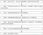
图1是本发明实施例FDSOI上锗硅鳍体的制作方法的流程图;1 is a flowchart of a method for fabricating a silicon germanium fin body on an FDSOI according to an embodiment of the present invention;
图2A-图2I是本发明实施例FDSOI上锗硅鳍体的制作方法各步骤中的器件结构示意图。2A-2I are schematic diagrams of device structures in each step of a method for fabricating a silicon germanium fin body on an FDSOI according to an embodiment of the present invention.
具体实施方式Detailed ways
如图1所示,是本发明实施例FDSOI上锗硅鳍体4的制作方法的流程图;如图2A至图2I所示,是本发明实施例FDSOI上锗硅鳍体4的制作方法各步骤中的器件结构示意图;本发明实施例FDSOI上锗硅鳍体4的制作方法包括如下步骤:As shown in FIG. 1 , it is a flow chart of a method for fabricating a silicon germanium
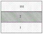
步骤一、如图2A所示,提供SOI基片,所述SOI基片包括底部体硅1、绝缘介质埋层2和顶层硅101,所述绝缘介质埋层2位于所述底部体硅1和所述顶层硅101之间。
本发明实施例中,所述绝缘介质埋层2为二氧化硅埋层。In the embodiment of the present invention, the insulating dielectric buried layer 2 is a silicon dioxide buried layer.
较佳为,所述SOI基片采用注氧隔离工艺形成。Preferably, the SOI substrate is formed by an oxygen injection isolation process.
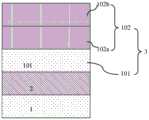
所述第一锗硅外延层102采用RPCVD工艺生长形成。The first silicon
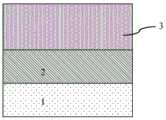
步骤二、如图2B所示,在所述顶层硅101表面外延生长第一锗硅外延层102,所述顶层硅101和所述第一锗硅外延层102叠加成顶层锗硅层3。Step 2: As shown in FIG. 2B , a first
本发明实施例中,生长的所述第一锗硅外延层102中的锗浓度具有从底部到顶部逐渐增加的分布。较佳为,生长的所述第一锗硅外延层102中的锗浓度具有从底部到顶部逐渐增加的梯度分布,图2B中显示了锗硅外延层102a和102b,锗硅外延层102a的锗浓度低于锗硅外延层102b的锗浓度。In the embodiment of the present invention, the concentration of germanium in the grown first silicon
生长的所述第一锗硅外延层102中的锗浓度为0~10%。图2B中,锗硅外延层102b的锗浓度为10%,锗硅外延层102b对应的分子式为Si0.9Ge0.1。The concentration of germanium in the grown first silicon
后续的最后形成的所述锗硅鳍体4的高度通过步骤二中的所述第一锗硅外延层102的厚度预先定义即进行所述锗硅鳍体4的高度粗调,所述第一锗硅外延层102的厚度同时保证避免产生位错缺陷。The height of the subsequently finally formed
本发明实施例中,步骤二完成后以及步骤三形成所述锗硅鳍体4前还包括对所述顶层锗硅层3进行锗浓度提升,通过循环进行如下分步骤实现:In the embodiment of the present invention, after the second step is completed and before the formation of the silicon
步骤21、如图2C所示,进行热氧化在所述顶层锗硅层3表面形成顶部氧化层103,所述顶层锗硅层3的厚度同时被减少;利用Si-O键结合能力强于Ge-O键的特点使所述顶部氧化层103为二氧化硅,且在所述顶部氧化层103和底部的所述顶层锗硅层3的界面处形成锗凝聚。Step 21: As shown in FIG. 2C, thermal oxidation is performed to form a
步骤22、如图2C所示,进行热退火将所述顶部氧化层103和所述顶层锗硅层3界面处凝聚的锗扩散到整个所述顶层锗硅层3。Step 22 , as shown in FIG. 2C , thermal annealing is performed to diffuse the condensed germanium at the interface between the
步骤23、如图2D所示,刻蚀去除所述顶部氧化层103。Step 23: As shown in FIG. 2D, the
本发明实施例中,步骤21至步骤23的循环次数为一次。在其他实施例中也能为:步骤21至步骤23的循环次数为大于1次;或者,取消步骤21至步骤23,直接进行后续的步骤三。In the embodiment of the present invention, the number of cycles from step 21 to step 23 is one time. In other embodiments, the number of cycles from steps 21 to 23 is greater than one; or, steps 21 to 23 are canceled, and the
步骤三、如图2E所示,形成由对所述顶层锗硅层3刻蚀后形成的锗硅鳍体4。Step 3: As shown in FIG. 2E , a silicon
本发明实施例中,采用侧墙硬质掩膜层定义所述锗硅鳍体4的形成区域,在所述侧墙硬质掩膜层的定义下进行刻蚀形成所述锗硅鳍体4。In the embodiment of the present invention, a spacer hard mask layer is used to define the formation region of the silicon
侧墙硬质掩膜层刻蚀工艺通常包括如下步骤:The sidewall hard mask layer etching process usually includes the following steps:
依次氧化层、氮化层和氧化层的ONO叠层;ONO stack of oxide layer, nitride layer and oxide layer in sequence;
之后再在ONO叠层上形成多晶硅层;Then a polysilicon layer is formed on the ONO stack;
之后进行光刻定义加刻蚀工艺在多晶硅层中形成沟槽;Then, a photolithography definition and etching process is performed to form trenches in the polysilicon layer;
之后形成硬质掩膜层如氮化硅组成的硬质掩膜层;Then form a hard mask layer such as a hard mask layer composed of silicon nitride;
对硬质掩膜层进行全面刻蚀在沟槽的侧面形成侧墙,该侧墙即为侧墙硬质掩膜层;The hard mask layer is fully etched to form a sidewall on the side of the trench, and the sidewall is the sidewall hard mask layer;
之后,去除多晶硅层;After that, remove the polysilicon layer;
之后,以侧墙硬质掩膜层为掩膜对底部的ONO叠层和所述顶层锗硅层3进行刻蚀形成所述锗硅鳍体4。Afterwards, the bottom ONO stack and the top layer of
步骤四、对所述锗硅鳍体4进行锗浓度提升,通过循环进行如下分步骤实现:Step 4: Raising the concentration of germanium on the silicon
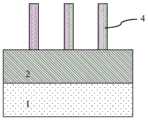
步骤41、如图2F所示,进行热氧化在所述锗硅鳍体4表面形成第一氧化层5,所述锗硅鳍体4的厚度同时被减少;利用Si-O键结合能力强于Ge-O键的特点使所述第一氧化层5为二氧化硅,且在所述第一氧化层5和所述锗硅鳍体4的界面处形成锗凝聚。Step 41: As shown in FIG. 2F, perform thermal oxidation to form a
本发明实施例中,步骤41中,热氧化采用干氧氧化。较佳为,步骤41中的所述热氧化的温度为500℃~1050℃。In the embodiment of the present invention, in step 41, the thermal oxidation adopts dry oxygen oxidation. Preferably, the temperature of the thermal oxidation in step 41 is 500°C to 1050°C.
步骤42、如图2F所示,进行热退火将所述第一氧化层5和所述锗硅鳍体4界面处凝聚的锗扩散到整个所述锗硅鳍体4。Step 42 , as shown in FIG. 2F , thermal annealing is performed to diffuse germanium condensed at the interface between the
本发明实施例中,步骤42中,所述第一氧化层5和所述绝缘介质埋层2作为锗扩散的阻挡层。In the embodiment of the present invention, in step 42, the
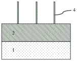
步骤43、如图2G所示,刻蚀去除所述第一氧化层5。Step 43 , as shown in FIG. 2G , the
本发明实施例中,步骤43中采用SiCoNi清洗工艺去除所述第一氧化层5。In the embodiment of the present invention, the SiCoNi cleaning process is used to remove the
步骤四中步骤41至步骤43的循环次数为一次以上,使锗浓度提升后的所述锗硅鳍体4的锗浓度的最大值达90%以上。In
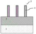
图2F-图2G对应于第一次循环做步骤41至步骤43时对应的器件结构图;而图2H-图2I则显示了第二次循环做步骤41至步骤43时对应的器件结构图,由图2H所示可知,在图2G所示的所述锗硅鳍体4的基础上进行步骤41并形成所述第一氧化层5b,图2H中所述第一氧化层单独用标记5b标出。之后,进行步骤42和步骤43,如图2I所示,步骤43完成后,去除了所述第一氧化层5b,由保留的所述锗硅鳍体4作为最后的所述锗硅鳍体4。Fig. 2F-Fig. 2G correspond to the device structure diagrams corresponding to the steps 41 to 43 in the first cycle; while Fig. 2H-Fig. 2I show the corresponding device structure diagrams when the second cycle is performed from steps 41 to 43, As shown in FIG. 2H, step 41 is performed on the basis of the silicon
随着循环次数的增加,所述锗硅鳍体4的锗浓度会不断增加,所述锗硅鳍体4的宽度和高度也会不断减少。步骤四完成后,所述锗硅鳍体4的高度为10nm~30nm,所述锗硅鳍体4的锗浓度的最大值达90%以上。As the number of cycles increases, the germanium concentration of the silicon
步骤四锗浓度提升完成后的所述锗硅鳍体4用于形成PMOS。In
所述PMOS器件包括栅极结构、源区、漏区和沟道区。The PMOS device includes a gate structure, a source region, a drain region and a channel region.
所述栅极结构形成于所述锗硅鳍体4的表面上,所述源区和所述漏区自对准形成在所述栅极结构两侧的所述锗硅鳍体4中,所述沟道区由位于所述源区和所述漏区之间的所述锗硅鳍体4组成,所述锗硅鳍体4的锗浓度的提升用于提高空穴载流子的迁移率。The gate structure is formed on the surface of the silicon
所述栅极结构包括叠加的栅介质层和栅极导电材料层。所述栅极结构包括叠加的栅介质层201和栅极导电材料层202。本发明实施例中,所述栅介质层201为栅氧化层,所述栅极导电材料层202为多晶硅栅。在其他实施例中也能为:所述栅介质层201为高介电常数层,所述栅极导电材料层202为金属栅。The gate structure includes a superimposed gate dielectric layer and a gate conductive material layer. The gate structure includes a stacked gate dielectric layer 201 and a gate conductive material layer 202 . In the embodiment of the present invention, the gate dielectric layer 201 is a gate oxide layer, and the gate conductive material layer 202 is a polysilicon gate. In other embodiments, the gate dielectric layer 201 can be a high dielectric constant layer, and the gate conductive material layer 202 can be a metal gate.
本发明实施例是在已经形成有绝缘介质埋层2的SOI基片的顶层硅101上外延第一锗硅外延层102来叠加形成顶层锗硅层3,之后再对顶层锗硅层3进行刻蚀形成锗硅鳍体4,之后再循环进行氧化、退火和刻蚀工艺实现对锗硅鳍体4的锗浓度提升同时实现锗硅鳍体4的宽度和高度的调节;氧化、退火和刻蚀工艺的循环工艺也简称为氧化(O)-刻蚀(E)-氧化(O)即OEO工艺,且本发明实施例的OEO工艺能对锗硅鳍体4进行3维处理,能最大限度的提升锗硅鳍体4的锗浓度如锗硅鳍体4的锗浓度的最大值能达90%以上以及能对锗硅鳍体4的宽度和高度进行精细调节;锗浓度提升后能使得锗硅鳍体4能很好的适用于PMOS的制作,能使PMOS的载流子迁移率得到提升,使PMOS的性能得到改善;锗硅鳍体4会作为器件的沟道区,沟道区的宽度对应于锗硅鳍体4的宽度,沟道区的高度对应于锗硅鳍体4的深度,在沟道区的宽度和高度方向上,沟道区都为量子阱结构,故本发明实施例通过对锗硅鳍体4的宽度和高度进行精细调节能实现对量子阱沟道区的宽度和深度进行精细调节。In the embodiment of the present invention, the first silicon
另外,相对于现有技术中锗硅外延层会先形成于体硅上之后在进行氧离子注入形成氧化物埋层的方法,本发明实施例的顶层锗硅层3对应的第一锗硅外延层102直接形成于SOI基片的顶层硅101上,第一锗硅外延层102的厚度能得到减少以及能使厚度得到很好的控制,也能使第一锗硅外延层102的外延质量得到提高,能避免出现第一锗硅外延层102较厚造成的位错缺陷;本发明实施例锗硅鳍体4的高度能第一锗硅外延层102的厚度预先定义即实现粗调,之后再在后续的OEO工艺中进行精细调节。In addition, compared with the prior art method in which the SiGe epitaxial layer is first formed on the bulk silicon and then the oxygen ion implantation is performed to form the buried oxide layer, the first SiGe epitaxy corresponding to the
以上通过具体实施例对本发明进行了详细的说明,但这些并非构成对本发明的限制。在不脱离本发明原理的情况下,本领域的技术人员还可做出许多变形和改进,这些也应视为本发明的保护范围。The present invention has been described in detail above through specific embodiments, but these are not intended to limit the present invention. Without departing from the principles of the present invention, those skilled in the art can also make many modifications and improvements, which should also be regarded as the protection scope of the present invention.
Claims (18)
Priority Applications (1)
| Application Number | Priority Date | Filing Date | Title |
|---|---|---|---|
| CN202010350253.7ACN111508844A (en) | 2020-04-28 | 2020-04-28 | Fabrication method of silicon germanium fin body on FDSOI |
Applications Claiming Priority (1)
| Application Number | Priority Date | Filing Date | Title |
|---|---|---|---|
| CN202010350253.7ACN111508844A (en) | 2020-04-28 | 2020-04-28 | Fabrication method of silicon germanium fin body on FDSOI |
Publications (1)
| Publication Number | Publication Date |
|---|---|
| CN111508844Atrue CN111508844A (en) | 2020-08-07 |
Family
ID=71865007
Family Applications (1)
| Application Number | Title | Priority Date | Filing Date |
|---|---|---|---|
| CN202010350253.7APendingCN111508844A (en) | 2020-04-28 | 2020-04-28 | Fabrication method of silicon germanium fin body on FDSOI |
Country Status (1)
| Country | Link |
|---|---|
| CN (1) | CN111508844A (en) |
Citations (6)
| Publication number | Priority date | Publication date | Assignee | Title |
|---|---|---|---|---|
| CN101866885A (en)* | 2009-04-17 | 2010-10-20 | 台湾积体电路制造股份有限公司 | Manufacturing method of FINFET element |
| US20150279973A1 (en)* | 2014-04-01 | 2015-10-01 | Globalfoundries Inc. | Methods of forming substantially defect-free, fully-strained silicon-germanium fins for a finfet semiconductor device |
| US20160049402A1 (en)* | 2014-08-18 | 2016-02-18 | Stmicroelectronics, Inc. | Semiconductor device having fins with in-situ doped, punch-through stopper layer and related methods |
| US20160071956A1 (en)* | 2014-09-05 | 2016-03-10 | International Business Machine Corporation | High germanium content silicon germanium fins |
| US20160190303A1 (en)* | 2014-12-31 | 2016-06-30 | Stmicroelectronics, Inc. | Silicon germanium-on-insulator finfet |
| CN105874601A (en)* | 2014-01-03 | 2016-08-17 | 高通股份有限公司 | Silicon germanium FinFET formation by Ge condensation |
- 2020
- 2020-04-28CNCN202010350253.7Apatent/CN111508844A/enactivePending
Patent Citations (6)
| Publication number | Priority date | Publication date | Assignee | Title |
|---|---|---|---|---|
| CN101866885A (en)* | 2009-04-17 | 2010-10-20 | 台湾积体电路制造股份有限公司 | Manufacturing method of FINFET element |
| CN105874601A (en)* | 2014-01-03 | 2016-08-17 | 高通股份有限公司 | Silicon germanium FinFET formation by Ge condensation |
| US20150279973A1 (en)* | 2014-04-01 | 2015-10-01 | Globalfoundries Inc. | Methods of forming substantially defect-free, fully-strained silicon-germanium fins for a finfet semiconductor device |
| US20160049402A1 (en)* | 2014-08-18 | 2016-02-18 | Stmicroelectronics, Inc. | Semiconductor device having fins with in-situ doped, punch-through stopper layer and related methods |
| US20160071956A1 (en)* | 2014-09-05 | 2016-03-10 | International Business Machine Corporation | High germanium content silicon germanium fins |
| US20160190303A1 (en)* | 2014-12-31 | 2016-06-30 | Stmicroelectronics, Inc. | Silicon germanium-on-insulator finfet |
Similar Documents
| Publication | Publication Date | Title |
|---|---|---|
| US10468408B2 (en) | Fin-like field effect transistor (FinFET) device and method of manufacturing same | |
| US9224737B2 (en) | Dual epitaxial process for a finFET device | |
| US10090300B2 (en) | Fin-like field effect transistor (FinFET) device and method of manufacturing same | |
| US9837321B2 (en) | Nonplanar device and strain-generating channel dielectric | |
| US9343551B2 (en) | Methods for manufacturing a fin structure of semiconductor device | |
| CN104124273B (en) | There is MOS device of strained buffer layer and forming method thereof | |
| US9589848B2 (en) | FinFET structures having silicon germanium and silicon channels | |
| TWI620314B (en) | Electrically insulating fin structure with alternative channel material and method of making same | |
| CN103094089B (en) | Fin formula field effect transistor gate oxide | |
| CN105321822B (en) | Channel strain control for non-planar compound semiconductor devices | |
| JP5728444B2 (en) | Semiconductor device and manufacturing method thereof | |
| US20120068268A1 (en) | Transistor structure and method of fabricating the same | |
| CN103681347A (en) | Method of making a FinFET device | |
| CN102034714A (en) | Method for forming isolated fin structures on bulk semiconductor material | |
| CN101604705B (en) | Fin grids transistor surrounded with grid electrodes and manufacturing method thereof | |
| CN107452627B (en) | Manufacturing method of semiconductor device | |
| TW202443702A (en) | Manufacturing method of semiconductor apparatus | |
| WO2012013036A1 (en) | Semiconductor device and method for forming the same | |
| CN111584420A (en) | Fabrication method of top germanium silicon layer of FDSOI | |
| TW201635385A (en) | Semiconductor device manufacturing method | |
| TWI805947B (en) | Horizontal gaa nano-wire and nano-slab transistors | |
| CN104637814B (en) | A kind of fin formula field effect transistor and preparation method thereof | |
| CN108962823B (en) | Semiconductor manufacturing method and semiconductor device | |
| CN102339860B (en) | Semiconductor device and method for manufacturing the same | |
| CN111508844A (en) | Fabrication method of silicon germanium fin body on FDSOI |
Legal Events
| Date | Code | Title | Description |
|---|---|---|---|
| PB01 | Publication | ||
| PB01 | Publication | ||
| SE01 | Entry into force of request for substantive examination | ||
| SE01 | Entry into force of request for substantive examination | ||
| RJ01 | Rejection of invention patent application after publication | Application publication date:20200807 | |
| RJ01 | Rejection of invention patent application after publication |