CN111508426B - Pixel circuit and driving method thereof, and display panel - Google Patents
Pixel circuit and driving method thereof, and display panelDownload PDFInfo
- Publication number
- CN111508426B CN111508426BCN202010479787.XACN202010479787ACN111508426BCN 111508426 BCN111508426 BCN 111508426BCN 202010479787 ACN202010479787 ACN 202010479787ACN 111508426 BCN111508426 BCN 111508426B
- Authority
- CN
- China
- Prior art keywords
- node
- circuit
- transistor
- terminal
- sub
- Prior art date
- Legal status (The legal status is an assumption and is not a legal conclusion. Google has not performed a legal analysis and makes no representation as to the accuracy of the status listed.)
- Active
Links
Images


Classifications
- G—PHYSICS
- G09—EDUCATION; CRYPTOGRAPHY; DISPLAY; ADVERTISING; SEALS
- G09G—ARRANGEMENTS OR CIRCUITS FOR CONTROL OF INDICATING DEVICES USING STATIC MEANS TO PRESENT VARIABLE INFORMATION
- G09G3/00—Control arrangements or circuits, of interest only in connection with visual indicators other than cathode-ray tubes
- G09G3/20—Control arrangements or circuits, of interest only in connection with visual indicators other than cathode-ray tubes for presentation of an assembly of a number of characters, e.g. a page, by composing the assembly by combination of individual elements arranged in a matrix no fixed position being assigned to or needed to be assigned to the individual characters or partial characters
- G09G3/22—Control arrangements or circuits, of interest only in connection with visual indicators other than cathode-ray tubes for presentation of an assembly of a number of characters, e.g. a page, by composing the assembly by combination of individual elements arranged in a matrix no fixed position being assigned to or needed to be assigned to the individual characters or partial characters using controlled light sources
- G09G3/30—Control arrangements or circuits, of interest only in connection with visual indicators other than cathode-ray tubes for presentation of an assembly of a number of characters, e.g. a page, by composing the assembly by combination of individual elements arranged in a matrix no fixed position being assigned to or needed to be assigned to the individual characters or partial characters using controlled light sources using electroluminescent panels
- G09G3/32—Control arrangements or circuits, of interest only in connection with visual indicators other than cathode-ray tubes for presentation of an assembly of a number of characters, e.g. a page, by composing the assembly by combination of individual elements arranged in a matrix no fixed position being assigned to or needed to be assigned to the individual characters or partial characters using controlled light sources using electroluminescent panels semiconductive, e.g. using light-emitting diodes [LED]
- G09G3/3208—Control arrangements or circuits, of interest only in connection with visual indicators other than cathode-ray tubes for presentation of an assembly of a number of characters, e.g. a page, by composing the assembly by combination of individual elements arranged in a matrix no fixed position being assigned to or needed to be assigned to the individual characters or partial characters using controlled light sources using electroluminescent panels semiconductive, e.g. using light-emitting diodes [LED] organic, e.g. using organic light-emitting diodes [OLED]
- G09G3/3225—Control arrangements or circuits, of interest only in connection with visual indicators other than cathode-ray tubes for presentation of an assembly of a number of characters, e.g. a page, by composing the assembly by combination of individual elements arranged in a matrix no fixed position being assigned to or needed to be assigned to the individual characters or partial characters using controlled light sources using electroluminescent panels semiconductive, e.g. using light-emitting diodes [LED] organic, e.g. using organic light-emitting diodes [OLED] using an active matrix
- G09G3/3258—Control arrangements or circuits, of interest only in connection with visual indicators other than cathode-ray tubes for presentation of an assembly of a number of characters, e.g. a page, by composing the assembly by combination of individual elements arranged in a matrix no fixed position being assigned to or needed to be assigned to the individual characters or partial characters using controlled light sources using electroluminescent panels semiconductive, e.g. using light-emitting diodes [LED] organic, e.g. using organic light-emitting diodes [OLED] using an active matrix with pixel circuitry controlling the voltage across the light-emitting element
- G—PHYSICS
- G09—EDUCATION; CRYPTOGRAPHY; DISPLAY; ADVERTISING; SEALS
- G09G—ARRANGEMENTS OR CIRCUITS FOR CONTROL OF INDICATING DEVICES USING STATIC MEANS TO PRESENT VARIABLE INFORMATION
- G09G3/00—Control arrangements or circuits, of interest only in connection with visual indicators other than cathode-ray tubes
- G09G3/20—Control arrangements or circuits, of interest only in connection with visual indicators other than cathode-ray tubes for presentation of an assembly of a number of characters, e.g. a page, by composing the assembly by combination of individual elements arranged in a matrix no fixed position being assigned to or needed to be assigned to the individual characters or partial characters
- G09G3/22—Control arrangements or circuits, of interest only in connection with visual indicators other than cathode-ray tubes for presentation of an assembly of a number of characters, e.g. a page, by composing the assembly by combination of individual elements arranged in a matrix no fixed position being assigned to or needed to be assigned to the individual characters or partial characters using controlled light sources
- G09G3/30—Control arrangements or circuits, of interest only in connection with visual indicators other than cathode-ray tubes for presentation of an assembly of a number of characters, e.g. a page, by composing the assembly by combination of individual elements arranged in a matrix no fixed position being assigned to or needed to be assigned to the individual characters or partial characters using controlled light sources using electroluminescent panels
- G09G3/32—Control arrangements or circuits, of interest only in connection with visual indicators other than cathode-ray tubes for presentation of an assembly of a number of characters, e.g. a page, by composing the assembly by combination of individual elements arranged in a matrix no fixed position being assigned to or needed to be assigned to the individual characters or partial characters using controlled light sources using electroluminescent panels semiconductive, e.g. using light-emitting diodes [LED]
- G09G3/3208—Control arrangements or circuits, of interest only in connection with visual indicators other than cathode-ray tubes for presentation of an assembly of a number of characters, e.g. a page, by composing the assembly by combination of individual elements arranged in a matrix no fixed position being assigned to or needed to be assigned to the individual characters or partial characters using controlled light sources using electroluminescent panels semiconductive, e.g. using light-emitting diodes [LED] organic, e.g. using organic light-emitting diodes [OLED]
- G09G3/3225—Control arrangements or circuits, of interest only in connection with visual indicators other than cathode-ray tubes for presentation of an assembly of a number of characters, e.g. a page, by composing the assembly by combination of individual elements arranged in a matrix no fixed position being assigned to or needed to be assigned to the individual characters or partial characters using controlled light sources using electroluminescent panels semiconductive, e.g. using light-emitting diodes [LED] organic, e.g. using organic light-emitting diodes [OLED] using an active matrix
- G09G3/3233—Control arrangements or circuits, of interest only in connection with visual indicators other than cathode-ray tubes for presentation of an assembly of a number of characters, e.g. a page, by composing the assembly by combination of individual elements arranged in a matrix no fixed position being assigned to or needed to be assigned to the individual characters or partial characters using controlled light sources using electroluminescent panels semiconductive, e.g. using light-emitting diodes [LED] organic, e.g. using organic light-emitting diodes [OLED] using an active matrix with pixel circuitry controlling the current through the light-emitting element
- G—PHYSICS
- G09—EDUCATION; CRYPTOGRAPHY; DISPLAY; ADVERTISING; SEALS
- G09G—ARRANGEMENTS OR CIRCUITS FOR CONTROL OF INDICATING DEVICES USING STATIC MEANS TO PRESENT VARIABLE INFORMATION
- G09G3/00—Control arrangements or circuits, of interest only in connection with visual indicators other than cathode-ray tubes
- G09G3/20—Control arrangements or circuits, of interest only in connection with visual indicators other than cathode-ray tubes for presentation of an assembly of a number of characters, e.g. a page, by composing the assembly by combination of individual elements arranged in a matrix no fixed position being assigned to or needed to be assigned to the individual characters or partial characters
- G09G3/22—Control arrangements or circuits, of interest only in connection with visual indicators other than cathode-ray tubes for presentation of an assembly of a number of characters, e.g. a page, by composing the assembly by combination of individual elements arranged in a matrix no fixed position being assigned to or needed to be assigned to the individual characters or partial characters using controlled light sources
- G09G3/30—Control arrangements or circuits, of interest only in connection with visual indicators other than cathode-ray tubes for presentation of an assembly of a number of characters, e.g. a page, by composing the assembly by combination of individual elements arranged in a matrix no fixed position being assigned to or needed to be assigned to the individual characters or partial characters using controlled light sources using electroluminescent panels
- G09G3/32—Control arrangements or circuits, of interest only in connection with visual indicators other than cathode-ray tubes for presentation of an assembly of a number of characters, e.g. a page, by composing the assembly by combination of individual elements arranged in a matrix no fixed position being assigned to or needed to be assigned to the individual characters or partial characters using controlled light sources using electroluminescent panels semiconductive, e.g. using light-emitting diodes [LED]
- G09G3/3208—Control arrangements or circuits, of interest only in connection with visual indicators other than cathode-ray tubes for presentation of an assembly of a number of characters, e.g. a page, by composing the assembly by combination of individual elements arranged in a matrix no fixed position being assigned to or needed to be assigned to the individual characters or partial characters using controlled light sources using electroluminescent panels semiconductive, e.g. using light-emitting diodes [LED] organic, e.g. using organic light-emitting diodes [OLED]
- G—PHYSICS
- G09—EDUCATION; CRYPTOGRAPHY; DISPLAY; ADVERTISING; SEALS
- G09G—ARRANGEMENTS OR CIRCUITS FOR CONTROL OF INDICATING DEVICES USING STATIC MEANS TO PRESENT VARIABLE INFORMATION
- G09G2300/00—Aspects of the constitution of display devices
- G09G2300/04—Structural and physical details of display devices
- G09G2300/0421—Structural details of the set of electrodes
- G09G2300/0426—Layout of electrodes and connections
- G—PHYSICS
- G09—EDUCATION; CRYPTOGRAPHY; DISPLAY; ADVERTISING; SEALS
- G09G—ARRANGEMENTS OR CIRCUITS FOR CONTROL OF INDICATING DEVICES USING STATIC MEANS TO PRESENT VARIABLE INFORMATION
- G09G2300/00—Aspects of the constitution of display devices
- G09G2300/08—Active matrix structure, i.e. with use of active elements, inclusive of non-linear two terminal elements, in the pixels together with light emitting or modulating elements
- G09G2300/0809—Several active elements per pixel in active matrix panels
- G09G2300/0819—Several active elements per pixel in active matrix panels used for counteracting undesired variations, e.g. feedback or autozeroing
- G—PHYSICS
- G09—EDUCATION; CRYPTOGRAPHY; DISPLAY; ADVERTISING; SEALS
- G09G—ARRANGEMENTS OR CIRCUITS FOR CONTROL OF INDICATING DEVICES USING STATIC MEANS TO PRESENT VARIABLE INFORMATION
- G09G2300/00—Aspects of the constitution of display devices
- G09G2300/08—Active matrix structure, i.e. with use of active elements, inclusive of non-linear two terminal elements, in the pixels together with light emitting or modulating elements
- G09G2300/0809—Several active elements per pixel in active matrix panels
- G09G2300/0842—Several active elements per pixel in active matrix panels forming a memory circuit, e.g. a dynamic memory with one capacitor
- G09G2300/0861—Several active elements per pixel in active matrix panels forming a memory circuit, e.g. a dynamic memory with one capacitor with additional control of the display period without amending the charge stored in a pixel memory, e.g. by means of additional select electrodes
- G—PHYSICS
- G09—EDUCATION; CRYPTOGRAPHY; DISPLAY; ADVERTISING; SEALS
- G09G—ARRANGEMENTS OR CIRCUITS FOR CONTROL OF INDICATING DEVICES USING STATIC MEANS TO PRESENT VARIABLE INFORMATION
- G09G2310/00—Command of the display device
- G09G2310/02—Addressing, scanning or driving the display screen or processing steps related thereto
- G09G2310/0243—Details of the generation of driving signals
- G09G2310/0251—Precharge or discharge of pixel before applying new pixel voltage
- G—PHYSICS
- G09—EDUCATION; CRYPTOGRAPHY; DISPLAY; ADVERTISING; SEALS
- G09G—ARRANGEMENTS OR CIRCUITS FOR CONTROL OF INDICATING DEVICES USING STATIC MEANS TO PRESENT VARIABLE INFORMATION
- G09G2310/00—Command of the display device
- G09G2310/02—Addressing, scanning or driving the display screen or processing steps related thereto
- G09G2310/0262—The addressing of the pixel, in a display other than an active matrix LCD, involving the control of two or more scan electrodes or two or more data electrodes, e.g. pixel voltage dependent on signals of two data electrodes
- G—PHYSICS
- G09—EDUCATION; CRYPTOGRAPHY; DISPLAY; ADVERTISING; SEALS
- G09G—ARRANGEMENTS OR CIRCUITS FOR CONTROL OF INDICATING DEVICES USING STATIC MEANS TO PRESENT VARIABLE INFORMATION
- G09G2310/00—Command of the display device
- G09G2310/06—Details of flat display driving waveforms
- G09G2310/061—Details of flat display driving waveforms for resetting or blanking
- G—PHYSICS
- G09—EDUCATION; CRYPTOGRAPHY; DISPLAY; ADVERTISING; SEALS
- G09G—ARRANGEMENTS OR CIRCUITS FOR CONTROL OF INDICATING DEVICES USING STATIC MEANS TO PRESENT VARIABLE INFORMATION
- G09G2320/00—Control of display operating conditions
- G09G2320/04—Maintaining the quality of display appearance
- G09G2320/043—Preventing or counteracting the effects of ageing
- G09G2320/045—Compensation of drifts in the characteristics of light emitting or modulating elements
Landscapes
- Engineering & Computer Science (AREA)
- Physics & Mathematics (AREA)
- Computer Hardware Design (AREA)
- General Physics & Mathematics (AREA)
- Theoretical Computer Science (AREA)
- Control Of El Displays (AREA)
- Control Of Indicators Other Than Cathode Ray Tubes (AREA)
- Electroluminescent Light Sources (AREA)
Abstract
Description
Translated fromChinese技术领域technical field
本公开涉及显示技术领域,尤其涉及一种像素电路及其驱动方法、显示面板。The present disclosure relates to the field of display technology, and in particular, to a pixel circuit and a driving method thereof, and a display panel.
背景技术Background technique
随着显示技术的发展,自发光显示装置,例如,有机发光二极管(organic lightemitting diode,OLED)、微型发光二极管(Micro Light Emitting Diode,Micro LED),迷你发光二极管(Mini Light Emitting Diode,Mini LED)等显示装置因具有自发光、对比度高、能耗低、视角广、响应速度快等特点,具有广阔的发展前景。With the development of display technology, self-luminous display devices, such as organic light emitting diode (OLED), micro light emitting diode (Micro Light Emitting Diode, Micro LED), mini light emitting diode (Mini Light Emitting Diode, Mini LED) Such display devices have broad development prospects due to their characteristics of self-luminescence, high contrast, low energy consumption, wide viewing angle, and fast response speed.
发明内容SUMMARY OF THE INVENTION
本公开的实施例提供一种像素电路及其驱动方法、显示面板,用于降低显示画面发生闪烁现象的几率。Embodiments of the present disclosure provide a pixel circuit, a driving method thereof, and a display panel, which are used to reduce the probability of flickering on a display screen.
为达到上述目的,本公开的实施例采用如下技术方案:In order to achieve the above object, the embodiments of the present disclosure adopt the following technical solutions:
一方面,本公开实施例提供一种像素电路,该像素电路包括:驱动子电路、第一复位子电路、写入子电路、发光器件和发光控制子电路。所述驱动子电路包括:驱动晶体管和存储电容;所述驱动晶体管的栅极与第一节点连接,驱动晶体管的第一极与第二节点连接,驱动晶体管的第二极与第三节点连接;存储电容,包括第一存储电极和第二存储电极,所述第一存储电极与所述第一节点连接,所述第二存储电极与第一电压端连接。所述第一复位子电路,至少连接所述第三节点、第一复位信号端和初始化信号端;所述第一复位子电路被配置为在初始化阶段,至少在所述第一复位信号端接收的第一复位信号的控制下,将来自所述初始化信号端的初始化信号传输至所述第三节点。所述写入子电路,连接第一扫描端、第二扫描端、数据端、所述第一节点、所述第二节点和所述第三节点;所述写入子电路被配置为在所述初始化阶段,在所述第一扫描端接收的第一扫描信号的控制下,将所述第三节点上的所述初始化信号传输至所述第一节点,以对所述第一节点进行复位;在数据写入阶段,在所述第一扫描端接收的所述第一扫描信号和所述第二扫描端接收的第二扫描信号的控制下,将所述数据端接收的数据信号写入至所述第一节点并对所述驱动晶体管进行阈值电压补偿。所述发光器件,包括阳极和阴极,所述阴极连接第二电压端。所述发光控制子电路,连接所述第二节点、所述第三节点、所述第一电压端、第一使能信号端、第二使能信号端和所述发光器件的阳极;所述发光控制子电路被配置为在发光阶段,在所述第一使能信号端接收的第一使能信号和所述第二使能信号端接收的第二使能信号的控制下,将所述第一电压端的电压信号传输至所述第二节点,并将所述驱动晶体管输出的电流传输至所述发光器件,以使所述发光器件发光。In one aspect, an embodiment of the present disclosure provides a pixel circuit including: a driving subcircuit, a first reset subcircuit, a writing subcircuit, a light emitting device, and a light emission control subcircuit. The drive sub-circuit comprises: a drive transistor and a storage capacitor; the gate of the drive transistor is connected to the first node, the first pole of the drive transistor is connected to the second node, and the second pole of the drive transistor is connected to the third node; The storage capacitor includes a first storage electrode and a second storage electrode, the first storage electrode is connected to the first node, and the second storage electrode is connected to the first voltage terminal. The first reset sub-circuit is connected to at least the third node, the first reset signal terminal and the initialization signal terminal; the first reset sub-circuit is configured to receive at least the first reset signal terminal in the initialization stage Under the control of the first reset signal, the initialization signal from the initialization signal terminal is transmitted to the third node. The writing sub-circuit is connected to the first scanning terminal, the second scanning terminal, the data terminal, the first node, the second node and the third node; the writing sub-circuit is configured to In the initialization phase, under the control of the first scan signal received by the first scan terminal, the initialization signal on the third node is transmitted to the first node to reset the first node ; In the data writing stage, under the control of the first scan signal received by the first scan end and the second scan signal received by the second scan end, the data signal received by the data end is written into to the first node and perform threshold voltage compensation on the drive transistor. The light-emitting device includes an anode and a cathode, and the cathode is connected to the second voltage terminal. the light-emitting control sub-circuit is connected to the second node, the third node, the first voltage terminal, the first enable signal terminal, the second enable signal terminal and the anode of the light-emitting device; the The lighting control sub-circuit is configured to, in the lighting stage, under the control of the first enable signal received by the first enable signal terminal and the second enable signal received by the second enable signal terminal, the The voltage signal of the first voltage terminal is transmitted to the second node, and the current output by the driving transistor is transmitted to the light emitting device, so that the light emitting device emits light.
在一些实施例中,所述像素电路还包括:第二复位子电路。所述第二复位子电路,连接所述发光器件的阳极、第二复位信号端和所述初始化信号端;所述第二复位子电路被配置为在所述初始化阶段或所述数据写入阶段,在所述第二复位信号端接收的第二复位信号的控制下,将来自所述初始化信号端的所述初始化信号传输至所述发光器件的阳极,对所述阳极进行复位。In some embodiments, the pixel circuit further includes: a second reset subcircuit. the second reset sub-circuit is connected to the anode of the light emitting device, the second reset signal terminal and the initialization signal terminal; the second reset sub-circuit is configured to be in the initialization phase or the data writing phase and, under the control of the second reset signal received by the second reset signal terminal, the initialization signal from the initialization signal terminal is transmitted to the anode of the light-emitting device, and the anode is reset.
在一些实施例中,所述第一复位信号端和所述第二复位信号端连接同一复位信号端。In some embodiments, the first reset signal terminal and the second reset signal terminal are connected to the same reset signal terminal.
在一些实施例中,所述发光控制子电路包括第一子电路和第二子电路。所述第一子电路连接所述第二节点、所述第一电压端和所述第一使能信号端;所述第一子电路被配置为在发光阶段,在所述第一使能信号端的所述第一使能信号的控制下,将所述第一电压端的电压信号传输至所述第二节点;所述第二子电路连接所述第三节点、所述第二使能信号端和所述发光器件的阳极;所述第二子电路被配置为在发光阶段,在所述第二使能信号端的所述第二使能信号的控制下,将所述驱动晶体管输出的电流传输至所述发光器件。In some embodiments, the lighting control subcircuit includes a first subcircuit and a second subcircuit. The first sub-circuit is connected to the second node, the first voltage terminal and the first enable signal terminal; the first sub-circuit is configured to be in the light-emitting phase, at the first enable signal Under the control of the first enable signal of the terminal, the voltage signal of the first voltage terminal is transmitted to the second node; the second sub-circuit is connected to the third node and the second enable signal terminal and the anode of the light-emitting device; the second sub-circuit is configured to transmit the current output by the driving transistor under the control of the second enable signal at the second enable signal terminal in the light-emitting phase to the light-emitting device.
在一些实施例中,所述第一使能信号端、所述第二使能信号端连接同一使能信号端。In some embodiments, the first enable signal terminal and the second enable signal terminal are connected to the same enable signal terminal.
在一些实施例中,所述初始化信号端与所述发光器件的阳极连接。In some embodiments, the initialization signal terminal is connected to the anode of the light emitting device.
在一些实施例中,所述第二子电路与所述第一复位子电路复用,所述第一复位信号端与所述第二使能信号端为同一信号端;所述信号端被配置在所述初始化阶段输出所述第一复位信号,在所述发光阶段输出所述第二使能信号。In some embodiments, the second sub-circuit is multiplexed with the first reset sub-circuit, the first reset signal terminal and the second enable signal terminal are the same signal terminal; the signal terminal is configured The first reset signal is output in the initialization phase, and the second enable signal is output in the light-emitting phase.
在一些实施例中,所述第一扫描端和所述第二扫描端连接同一扫描端。In some embodiments, the first scan end and the second scan end are connected to the same scan end.
在一些实施例中,所述写入子电路包括第三子电路和第四子电路。所述第三子电路连接所述第二扫描端、所述数据端和所述第二节点;所述第三子电路被配置为在所述第二扫描端的所述第二扫描信号的控制下,至少在数据写入阶段开启,将所述数据端接收的数据信号传输至所述第二节点;所述第四子电路连接所述第一扫描端、所述第一节点和所述第三节点,所述第四子电路被配置为在所述第一扫描端接收的所述第一扫描信号的控制下,在所述初始化阶段和所述数据写入阶段开启,并在所述初始化阶段将所述第三节点上的所述初始化信号传输至所述第一节点,在所述数据写入阶段将所述第二节点的所述数据信号写入至所述第一节点并对所述驱动晶体管进行阈值电压补偿。In some embodiments, the write subcircuit includes a third subcircuit and a fourth subcircuit. the third sub-circuit is connected to the second scan terminal, the data terminal and the second node; the third sub-circuit is configured to be under the control of the second scan signal of the second scan terminal , is turned on at least in the data writing stage, and transmits the data signal received by the data terminal to the second node; the fourth sub-circuit is connected to the first scan terminal, the first node and the third node, the fourth sub-circuit is configured to be turned on in the initialization phase and the data writing phase under the control of the first scan signal received by the first scan terminal, and is turned on in the initialization phase The initialization signal on the third node is transmitted to the first node, the data signal of the second node is written to the first node during the data write phase and the The drive transistor performs threshold voltage compensation.
在一些实施例中,所述第一复位子电路包括第一晶体管,所述第一晶体管的栅极连接所述第一复位信号端,所述第一晶体管的第一极连接所述初始化信号端,所述第一晶体管的第二极连接所述第三节点。In some embodiments, the first reset sub-circuit includes a first transistor, a gate of the first transistor is connected to the first reset signal terminal, and a first electrode of the first transistor is connected to the initialization signal terminal , the second electrode of the first transistor is connected to the third node.
在一些实施例中,所述第二复位子电路包括第二晶体管,所述第二晶体管的栅极连接所述第二复位信号端,所述第二晶体管的第一极连接所述初始化信号端,所述第二晶体管的第二极连接所述发光器件的阳极。In some embodiments, the second reset sub-circuit includes a second transistor, a gate of the second transistor is connected to the second reset signal terminal, and a first electrode of the second transistor is connected to the initialization signal terminal , the second electrode of the second transistor is connected to the anode of the light emitting device.
在一些实施例中,所述第一子电路包括第三晶体管,所述第三晶体管的栅极连接所述第一使能信号端,所述第三晶体管的第一极连接所述第一电压端,所述第三晶体管的第二极连接所述第二节点;所述第二子电路包括第四晶体管,所述第四晶体管的栅极连接所述第二使能信号端,所述第四晶体管的第一极连接所述第三节点,所述第四晶体管的第二极连接所述发光器件的阳极。In some embodiments, the first sub-circuit includes a third transistor, a gate of the third transistor is connected to the first enable signal terminal, and a first electrode of the third transistor is connected to the first voltage terminal, the second pole of the third transistor is connected to the second node; the second sub-circuit includes a fourth transistor, the gate of the fourth transistor is connected to the second enable signal terminal, the first The first electrode of the four transistors is connected to the third node, and the second electrode of the fourth transistor is connected to the anode of the light emitting device.
在一些实施例中,所述第三子电路包括第五晶体管,所述第五晶体管的栅极连接所述第二扫描端,所述第五晶体管的第一极连接所述数据端,所述第五晶体管的第二极连接所述第二节点。In some embodiments, the third sub-circuit includes a fifth transistor, the gate of the fifth transistor is connected to the second scan terminal, the first electrode of the fifth transistor is connected to the data terminal, the The second electrode of the fifth transistor is connected to the second node.
在一些实施例中,所述第四子电路包括第六晶体管,所述第六晶体管的栅极连接所述第一扫描端,所述第六晶体管的第一极连接所述第三节点,所述第六晶体管的第二极连接所述第一节点。In some embodiments, the fourth sub-circuit includes a sixth transistor, a gate of the sixth transistor is connected to the first scan terminal, a first electrode of the sixth transistor is connected to the third node, so The second electrode of the sixth transistor is connected to the first node.
在一些实施例中,所述第四子电路包括第七晶体管和第八晶体管;所述第七晶体管的栅极与所述第一扫描端连接,所述第七晶体管的第一极与所述第三节点连接,所述第七晶体管的第二极与第四节点连接;所述第八晶体管的栅极与所述第一扫描端连接,所述第八晶体管的第一极与所述第四节点连接,所述第八晶体管的第二极与所述第一节点连接。In some embodiments, the fourth sub-circuit includes a seventh transistor and an eighth transistor; the gate of the seventh transistor is connected to the first scan terminal, and the first pole of the seventh transistor is connected to the first scan terminal. The third node is connected, the second pole of the seventh transistor is connected to the fourth node; the gate of the eighth transistor is connected to the first scan terminal, and the first pole of the eighth transistor is connected to the first scan terminal. Four nodes are connected, and the second pole of the eighth transistor is connected to the first node.
在一些实施例中,所述第一复位子电路包括第九晶体管和所述第七晶体管;所述第九晶体管的栅极与所述第一复位信号端连接,所述第九晶体管的第一极与所述初始化信号端连接,所述第九晶体管的第二极与所述第四节点连接。In some embodiments, the first reset sub-circuit includes a ninth transistor and the seventh transistor; the gate of the ninth transistor is connected to the first reset signal terminal, and the first reset signal terminal of the ninth transistor The pole is connected to the initialization signal terminal, and the second pole of the ninth transistor is connected to the fourth node.
另一方面,本公开实施例提供一种显示面板,包括上述像素电路。On the other hand, an embodiment of the present disclosure provides a display panel including the above-mentioned pixel circuit.
在一些实施例中,所述显示面板具有多个呈阵列排布的亚像素区,每个亚像素区设置有一个所述像素电路。所述显示面板还包括多条扫描线,位于同一行的所有像素电路连接的第一扫描端和第二扫描端均连接一条扫描线;或者,所述显示面板还包括多条第一扫描线和多条第二扫描线,位于同一行的所有像素电路连接的第一扫描端和第二扫描端分别连接第一扫描线和第二扫描线。In some embodiments, the display panel has a plurality of sub-pixel regions arranged in an array, and each sub-pixel region is provided with one of the pixel circuits. The display panel further includes a plurality of scan lines, and the first scan end and the second scan end connected to all pixel circuits in the same row are connected to one scan line; or, the display panel further includes a plurality of first scan lines and a second scan line. For the plurality of second scan lines, the first scan end and the second scan end connected to all pixel circuits in the same row are respectively connected to the first scan line and the second scan line.
在一些实施例中,位于同一行的所有像素电路连接的第一扫描端和第二扫描端均连接一条扫描线,位于第n行的所有像素电路连接的第一复位信号端连接与第n-1行像素电路对应的所述扫描线。In some embodiments, the first scan terminal and the second scan terminal connected to all pixel circuits in the same row are connected to one scan line, and the first reset signal terminal connected to all pixel circuits in the nth row is connected to the n-th The scan lines corresponding to one row of pixel circuits.
再一方面,本公开实施例提供一种上述像素电路的驱动方法,包括:在一图像帧的初始化阶段:向第一复位信号端输入第一复位信号,以使第一复位子电路将来自初始化信号端的初始化信号传输至第三节点;向第一扫描端输入第一扫描信号,以使写入子电路将所述第三节点上的所述初始化信号传输至第一节点,以对所述第一节点进行复位;在一图像帧的数据写入阶段:向所述第一扫描端输入所述第一扫描信号,向第二扫描端输入第二扫描信号,并向数据端输入数据信号,以使写入子电路将所述数据端接收的数据信号写入至所述第一节点,对驱动晶体管进行阈值电压补偿;在一图像帧的发光阶段:向第一使能信号端输入第一使能信号,并向第二使能信号端输入第二使能信号,以使发光控制子电路将第一电压端的电压信号传输至第二节点,并将所述驱动晶体管输出的电流传输至发光器件,使所述发光器件发光。In yet another aspect, an embodiment of the present disclosure provides a method for driving the above-mentioned pixel circuit, including: in an initialization stage of an image frame: inputting a first reset signal to a first reset signal terminal, so that the first reset sub-circuit will automatically reset the circuit from the initialization. The initialization signal of the signal terminal is transmitted to the third node; the first scan signal is input to the first scan terminal, so that the writing sub-circuit transmits the initialization signal on the third node to the first node, so that the first scan signal is transmitted to the first node. A node is reset; in the data writing stage of an image frame: the first scan signal is input to the first scan terminal, the second scan signal is input to the second scan terminal, and the data signal is input to the data terminal to The writing sub-circuit writes the data signal received by the data terminal to the first node, and performs threshold voltage compensation on the driving transistor; in the light-emitting stage of an image frame: inputting the first enable signal to the first enable signal terminal enable signal, and input the second enable signal to the second enable signal terminal, so that the light-emitting control sub-circuit transmits the voltage signal of the first voltage terminal to the second node, and transmits the current output by the driving transistor to the light-emitting device , so that the light-emitting device emits light.
在一些实施例中,所述驱动方法还包括:在一图像帧的初始化阶段,向所述数据端输入所述数据信号。In some embodiments, the driving method further includes: inputting the data signal to the data terminal in an initialization stage of an image frame.
本公开一些实施例提供的像素电路,写入子电路与第一节点(驱动晶体管的栅极)连接,第一复位子电路与第三节点连接,与相关技术中的像素电路相比,只有写入子电路与驱动晶体管的栅极直接连接。这样一来,对驱动晶体管的栅极电压的影响较小,在发光阶段,驱动晶体管的栅极的电压的变化量减小,从而对发光器件的发光性能影响降低,进而可以改善显示面板的发光性能,降低显示画面发生闪烁现象的几率。In the pixel circuit provided by some embodiments of the present disclosure, the writing sub-circuit is connected to the first node (the gate of the driving transistor), and the first reset sub-circuit is connected to the third node. Compared with the pixel circuit in the related art, only the writing sub-circuit is The input sub-circuit is directly connected to the gate of the driving transistor. In this way, the influence on the gate voltage of the driving transistor is small. In the light-emitting stage, the variation of the gate voltage of the driving transistor is reduced, thereby reducing the influence on the light-emitting performance of the light-emitting device, thereby improving the light-emitting of the display panel. performance and reduce the chance of flickering on the display screen.
附图说明Description of drawings
为了更清楚地说明本公开中的技术方案,下面将对本公开一些实施例中所需要使用的附图作简单地介绍,显而易见地,下面描述中的附图仅仅是本公开的一些实施例的附图,对于本领域普通技术人员来讲,还可以根据这些附图获得其他的附图。此外,以下描述中的附图可以视作示意图,并非对本公开实施例所涉及的产品的实际尺寸、方法的实际流程、信号的实际时序等的限制。In order to illustrate the technical solutions in the present disclosure more clearly, the following briefly introduces the accompanying drawings that need to be used in some embodiments of the present disclosure. Obviously, the accompanying drawings in the following description are only the appendixes of some embodiments of the present disclosure. For those of ordinary skill in the art, other drawings can also be obtained from these drawings. In addition, the accompanying drawings in the following description may be regarded as schematic diagrams, and are not intended to limit the actual size of the product involved in the embodiments of the present disclosure, the actual flow of the method, the actual timing of signals, and the like.
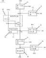
图1A为相关技术提供的一种驱动电路的结构图;1A is a structural diagram of a driving circuit provided by the related art;
图1B为相关技术提供的另一种驱动电路的结构图;FIG. 1B is a structural diagram of another driving circuit provided by the related art;
图1C为相关技术提供的一种像素电路中驱动晶体管栅极电压变化的示意图;1C is a schematic diagram of a gate voltage change of a driving transistor in a pixel circuit provided by the related art;
图2为本公开实施例提供的一种显示面板的俯视结构图;FIG. 2 is a top-view structural view of a display panel according to an embodiment of the present disclosure;
图3A为本公开实施例提供的一种像素电路的结构图;3A is a structural diagram of a pixel circuit according to an embodiment of the present disclosure;
图3B为本公开实施例提供的一种像素电路和相关技术提供的一种像素电路中的驱动晶体管栅极电压的模拟结果图;3B is a simulation result diagram of a gate voltage of a driving transistor in a pixel circuit provided by an embodiment of the present disclosure and a pixel circuit provided by a related art;
图4为本公开实施例提供的一种像素电路的驱动方法流程图;4 is a flowchart of a method for driving a pixel circuit according to an embodiment of the present disclosure;
图5为本公开实施例提供的另一种像素电路的结构图;FIG. 5 is a structural diagram of another pixel circuit provided by an embodiment of the present disclosure;
图6A为本公开实施例提供的一种显示面板的电路连接图;6A is a circuit connection diagram of a display panel according to an embodiment of the present disclosure;
图6B为本公开实施例提供的另一种显示面板的电路连接图;6B is a circuit connection diagram of another display panel according to an embodiment of the present disclosure;
图6C为本公开实施例提供的又一种显示面板的电路连接图;6C is a circuit connection diagram of still another display panel provided by an embodiment of the present disclosure;
图7为本公开实施例提供的一种像素电路的具体结构图;FIG. 7 is a specific structural diagram of a pixel circuit according to an embodiment of the present disclosure;
图8为图7所示的像素电路的时序控制图;8 is a timing control diagram of the pixel circuit shown in FIG. 7;
图9A为图7所示的像素电路在初始化阶段的示意图;9A is a schematic diagram of the pixel circuit shown in FIG. 7 in an initialization stage;
图9B为图7所示的像素电路在数据写入阶段的示意图;9B is a schematic diagram of the pixel circuit shown in FIG. 7 in a data writing stage;
图9C为图7所示的像素电路在发光阶段的示意图;9C is a schematic diagram of the pixel circuit shown in FIG. 7 in a light-emitting stage;
图10为本公开实施例提供的另一种像素电路的具体结构图;FIG. 10 is a specific structural diagram of another pixel circuit provided by an embodiment of the present disclosure;
图11为图10所示的像素电路的时序控制图;FIG. 11 is a timing control diagram of the pixel circuit shown in FIG. 10;
图12A为图10所示的像素电路在初始化阶段的示意图;12A is a schematic diagram of the pixel circuit shown in FIG. 10 in an initialization stage;
图12B为图10所示的像素电路在数据写入阶段的示意图;12B is a schematic diagram of the pixel circuit shown in FIG. 10 in a data writing stage;
图13为本公开实施例提供的一种像素电路中各信号的模拟结果图;FIG. 13 is a simulation result diagram of each signal in a pixel circuit according to an embodiment of the present disclosure;
图14为本公开实施例提供的又一种显示面板的电路连接图;FIG. 14 is a circuit connection diagram of still another display panel according to an embodiment of the present disclosure;
图15为图14所示显示面板中像素电路的时序控制图;FIG. 15 is a timing control diagram of a pixel circuit in the display panel shown in FIG. 14;
图16为本公开实施例提供的又一种像素电路的结构图;FIG. 16 is a structural diagram of yet another pixel circuit provided by an embodiment of the present disclosure;
图17为图16所示的像素电路的具体结构图;FIG. 17 is a specific structural diagram of the pixel circuit shown in FIG. 16;
图18为图17所示的像素电路的时序控制图;FIG. 18 is a timing control diagram of the pixel circuit shown in FIG. 17;
图19为本公开实施例提供的另一种像素电路中各信号的模拟结果图;FIG. 19 is a simulation result diagram of each signal in another pixel circuit provided by an embodiment of the present disclosure;
图20为本公开实施例提供的又一种像素电路的结构图;FIG. 20 is a structural diagram of yet another pixel circuit provided by an embodiment of the present disclosure;
图21为图20所示的像素电路的具体结构图;FIG. 21 is a specific structural diagram of the pixel circuit shown in FIG. 20;
图22为图21所示的像素电路的时序控制图;FIG. 22 is a timing control diagram of the pixel circuit shown in FIG. 21;
图23A为图21所示的像素电路在初始化阶段的示意图;23A is a schematic diagram of the pixel circuit shown in FIG. 21 in an initialization stage;
图23B为图21所示的像素电路在数据写入阶段的示意图;23B is a schematic diagram of the pixel circuit shown in FIG. 21 in a data writing stage;
图23C为图21所示的像素电路在发光阶段的示意图;23C is a schematic diagram of the pixel circuit shown in FIG. 21 in a light-emitting stage;
图24为本公开实施例提供的另一种像素电路中各信号的模拟结果图;FIG. 24 is a simulation result diagram of each signal in another pixel circuit provided by an embodiment of the present disclosure;
图25为本公开实施例提供的又一种像素电路的具体结构图;FIG. 25 is a specific structural diagram of yet another pixel circuit provided by an embodiment of the present disclosure;
图26为图25所示的像素电路的时序控制图;FIG. 26 is a timing control diagram of the pixel circuit shown in FIG. 25;
图27A为图25所示的像素电路在初始化阶段的示意图;FIG. 27A is a schematic diagram of the pixel circuit shown in FIG. 25 in an initialization stage;
图27B为图25所示的像素电路在数据写入阶段的示意图;27B is a schematic diagram of the pixel circuit shown in FIG. 25 in a data writing stage;
图27C为图25所示的像素电路在发光阶段的示意图;FIG. 27C is a schematic diagram of the pixel circuit shown in FIG. 25 in a light-emitting stage;
图28为本公开实施例提供的另一种像素电路中各信号的模拟结果图;FIG. 28 is a simulation result diagram of each signal in another pixel circuit provided by an embodiment of the present disclosure;
图29为本公开实施例提供的另一种像素电路和相关技术提供的一种像素电路中的驱动晶体管栅极电压的模拟结果图;FIG. 29 is a simulation result diagram of a gate voltage of a driving transistor in another pixel circuit provided by an embodiment of the present disclosure and a pixel circuit provided by a related art;
图30A为本公开实施例提供的又一种像素电路的结构图;30A is a structural diagram of yet another pixel circuit provided by an embodiment of the present disclosure;
图30B为图30A所示的像素电路的具体结构图。FIG. 30B is a specific structural diagram of the pixel circuit shown in FIG. 30A .
具体实施方式Detailed ways
下面将结合附图,对本公开一些实施例中的技术方案进行清楚、完整地描述,显然,所描述的实施例仅仅是本公开一部分实施例,而不是全部的实施例。基于本公开所提供的实施例,本领域普通技术人员所获得的所有其他实施例,都属于本公开保护的范围。The technical solutions in some embodiments of the present disclosure will be clearly and completely described below with reference to the accompanying drawings. Obviously, the described embodiments are only a part of the embodiments of the present disclosure, but not all of the embodiments. All other embodiments obtained by those of ordinary skill in the art based on the embodiments provided by the present disclosure fall within the protection scope of the present disclosure.
除非上下文另有要求,否则,在整个说明书和权利要求书中,术语“包括”被解释为开放、包含的意思,即为“包含,但不限于”。在说明书的描述中,术语“一个实施例”、“一些实施例”、“示例性实施例”、“示例”、“特定示例”或“一些示例”等旨在表明与该实施例或示例相关的特定特征、结构、材料或特性包括在本公开的至少一个实施例或示例中。上述术语的示意性表示不一定是指同一实施例或示例。此外,所述的特定特征、结构、材料或特点可以以任何适当方式包括在任何一个或多个实施例或示例中。Throughout the specification and claims, the term "comprising" is to be interpreted in an open, inclusive sense, ie, "including, but not limited to," unless the context requires otherwise. In the description of the specification, the terms "one embodiment," "some embodiments," "exemplary embodiment," "example," "particular example," or "some examples" and the like are intended to indicate associations with the embodiments or examples The particular feature, structure, material or characteristic of the present disclosure is included in at least one embodiment or example of the present disclosure. The schematic representations of the above terms are not necessarily referring to the same embodiment or example. Furthermore, the particular features, structures, materials or characteristics described may be included in any suitable manner in any one or more embodiments or examples.
以下,术语“第一”、“第二”仅用于描述目的,而不能理解为指示或暗示相对重要性或者隐含指明所指示的技术特征的数量。由此,限定有“第一”、“第二”的特征可以明示或者隐含地包括一个或者更多个该特征。在本公开实施例的描述中,除非另有说明,“多个”的含义是两个或两个以上。Hereinafter, the terms "first" and "second" are only used for descriptive purposes, and should not be construed as indicating or implying relative importance or implicitly indicating the number of indicated technical features. Thus, a feature defined as "first" or "second" may expressly or implicitly include one or more of that feature. In the description of the embodiments of the present disclosure, unless otherwise specified, "plurality" means two or more.
在描述一些实施例时,可能使用了“连接”的表达。例如,描述一些实施例时可能使用了术语“连接”以表明两个或两个以上部件彼此间有直接物理接触或电接触。In describing some embodiments, the expression "connected" may be used. For example, the term "connected" may be used in describing some embodiments to indicate that two or more components are in direct physical or electrical contact with each other.
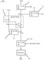
发光二极管(例如有机发光二极管)为电流驱动型器件,如图1A所示为相关技术中的一种用于驱动该发光二极管的驱动电路,该驱动电路由一个驱动晶体管Td、一个开关晶体管Ts和一个存储电容Cst组成。在该驱动电路驱动发光二极管L发光时,开关晶体管Ts的栅极接收扫描信号端G的扫描信号,开关晶体管Ts导通,数据信号端DE的数据信号通过开关晶体管Ts输入到驱动晶体管Td的栅极,驱动晶体管Td打开,第一电压端VDD、发光二极管L和第二电压端VSS导通,驱动晶体管Td产生的驱动电流驱动发光二极管L发光。在此过程中,数据信号端DE上的数据信号向导通的开关晶体管Ts所连接的存储电容Cst进行充电,存储电容Cst存储的电能使驱动晶体管Td保持开启,以维持一帧画面显示所需的时间。A light-emitting diode (such as an organic light-emitting diode) is a current-driven device, and as shown in FIG. 1A is a driving circuit for driving the light-emitting diode in the related art, the driving circuit consists of a driving transistor Td, a switching transistor Ts and A storage capacitor Cst is formed. When the driving circuit drives the light-emitting diode L to emit light, the gate of the switching transistor Ts receives the scanning signal from the scanning signal terminal G, the switching transistor Ts is turned on, and the data signal from the data signal terminal DE is input to the gate of the driving transistor Td through the switching transistor Ts pole, the driving transistor Td is turned on, the first voltage terminal VDD, the light emitting diode L and the second voltage terminal VSS are turned on, and the driving current generated by the driving transistor Td drives the light emitting diode L to emit light. During this process, the data signal on the data signal terminal DE charges the storage capacitor Cst connected to the turned-on switching transistor Ts, and the energy stored in the storage capacitor Cst keeps the driving transistor Td turned on, so as to maintain the required power for displaying one frame of image. time.
驱动晶体管Td的饱和电流公式为:The saturation current formula of the drive transistor Td is:
I=K(Vgs-Vth)2 (1)I=K(Vgs -Vth )2 (1)
其中,K为与驱动晶体管Td本身特性有关的系数,Vgs为驱动晶体管Td的栅源电压,Vth为驱动晶体管Td的阈值电压。Among them, K is a coefficient related to the characteristics of the driving transistor Td itself, Vgs is the gate-source voltage of the driving transistor Td, and Vth is the threshold voltage of the driving transistor Td.
在显示装置中,显示装置通常包括多个发光二极管L,相应的驱动这些发光二极管L发光的驱动电路也有多个。由于工艺制程的差异以及温度、器件老化等原因的影响,驱动晶体管Td的阈值电压Vth会产生漂移的现象,从而导致驱动晶体管Td提供给发光二极管L的驱动电流偏离目标电流值。由于不同驱动电路中的各个驱动晶体管Td的阈值电压Vth可能不同,因此,可能会导致各发光二极管L的发光亮度不一致,从而导致显示装置的显示不均匀。In a display device, the display device usually includes a plurality of light emitting diodes L, and there are also a plurality of corresponding driving circuits for driving the light emitting diodes L to emit light. The threshold voltage Vth of the driving transistor Td may drift due to differences in process, temperature, device aging, etc., so that the driving current provided by the driving transistor Td to the light-emitting diode L deviates from the target current value. Since the threshold voltages Vth of the driving transistors Td in different driving circuits may be different, the light-emitting luminances of the light-emitting diodes L may be inconsistent, resulting in uneven display of the display device.
为了改善驱动晶体管Td的阈值电压Vth漂移造成的影响,如图1B所示,在如图1A所示的驱动电路基础上增加了阈值电压补偿子电路101,以在驱动电路驱动发光二极管L发光前对驱动晶体管Td的阈值电压Vth进行补偿,消除阈值电压Vth漂移对显示装置的影响。In order to improve the influence caused by the drift of the threshold voltage Vth of the driving transistor Td, as shown in FIG. 1B , a threshold
此外,在一帧画面显示完成,进行下一帧画面显示前,驱动晶体管Td的栅极可能存在残余电压。为了消除一帧画面残余的电压对下一帧画面显示的影响,如图1B所示,驱动电路中还包括复位子电路102,以在下一帧画面显示前,对驱动晶体管Td的栅极进行复位。In addition, after the display of one frame is completed, there may be residual voltage on the gate of the driving transistor Td before the next frame is displayed. In order to eliminate the influence of the residual voltage of one frame on the display of the next frame, as shown in FIG. 1B , the driving circuit further includes a
在相关技术中,如图1B所示,阈值电压补偿子电路101和复位子电路102均电连接至第一节点N1(驱动晶体管Td的栅极),导致第一节点N1的电压受到阈值电压补偿子电路101和复位子电路102中的晶体管的影响。由于阈值电压补偿子电路101和复位子电路102均包括至少一个晶体管,晶体管存在漏电流,因此,会影响第一节点N1上的电压,从而导致Vgs发生变化。由公式1可知,Vgs变化,可能导致驱动电流I发生变化,从而导致发光二极管L的发光亮度改变,导致显示装置的显示画面发生闪烁(Flicker)现象。In the related art, as shown in FIG. 1B , the threshold
在相关技术中,Flicker测试结果如表1所示。In the related art, the Flicker test results are shown in Table 1.
表1Table 1

如表1所示,在显示装置以低驱动频率(例如低于40Hz)驱动的情况下,显示装置M1和显示装置M2均存在Flicker现象,且随着驱动频率的降低,Flicker现象越严重。例如在驱动频率为40Hz时,Flicker现象为等级一(L1),在驱动频率为20Hz时,Flicker现象为等级三(L3)。当驱动频率为15Hz时,显示装置出现滚动异常显示,当驱动频率为7.5Hz时,显示装置出现严重的滚动异常显示。As shown in Table 1, when the display device is driven at a low driving frequency (eg, lower than 40 Hz), the Flicker phenomenon exists in both the display device M1 and the display device M2, and as the driving frequency decreases, the Flicker phenomenon becomes more severe. For example, when the driving frequency is 40 Hz, the Flicker phenomenon is level one (L1), and when the driving frequency is 20 Hz, the Flicker phenomenon is level three (L3). When the driving frequency is 15 Hz, the display device exhibits abnormal scrolling display, and when the driving frequency is 7.5 Hz, the display device exhibits severe scrolling abnormal display.
上述Flicker现象产生原因为:如图1C所示,在发光阶段开始时,第一节点N1的电压为V1,在发光阶段持续时间内,阈值电压补偿子电路101和复位子电路102中的晶体管处于关闭状态,由于晶体管存在漏电流,导致在发光阶段,第一节点N1的电压不断变化。在发光阶段结束时,第一节点N1的电压为V2,在发光阶段的持续时间内,第一节点N1的电压变化量为△V。频率越低,一帧的时间越长,△V越大,发光二极管LED的亮度改变越剧烈,从而Flicker现象越严重。The above-mentioned Flicker phenomenon is caused by: as shown in FIG. 1C , at the beginning of the light-emitting phase, the voltage of the first node N1 is V1, and during the duration of the light-emitting phase, the transistors in the threshold
本公开的一些实施例提供一种显示面板,如图2所示,该显示面板包括多个像素电路100。Some embodiments of the present disclosure provide a display panel, as shown in FIG. 2 , the display panel includes a plurality of
在一些实施例中,如图2所示,该显示面板具有多个呈阵列排布的亚像素区P,每个亚像素区P设置有一个像素电路100。In some embodiments, as shown in FIG. 2 , the display panel has a plurality of sub-pixel regions P arranged in an array, and each sub-pixel region P is provided with a
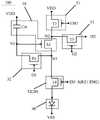
如图3A所示,本公开一些实施例提供的像素电路100包括:驱动子电路10、第一复位子电路20、写入子电路30、发光器件40和发光控制子电路50。As shown in FIG. 3A , the
驱动子电路10包括:驱动晶体管Td和存储电容Cst。驱动晶体管Td的栅极与第一节点N1连接,驱动晶体管Td的第一极与第二节点N2连接,驱动晶体管Td的第二极与第三节点N3连接。存储电容Cst包括第一存储电极和第二存储电极,第一存储电极与第一节点N1连接,第二存储电极与第一电压端VDD连接。The driving
驱动晶体管Td是指向发光器件40提供驱动电流的晶体管,驱动晶体管Td的宽长比大于起开关作用的晶体管的宽长比。The driving transistor Td is a transistor for supplying a driving current to the
第一复位子电路20,至少连接第三节点N3、第一复位信号端RE1和初始化信号端INI。第一复位信号端RE1被配置为接收第一复位信号,并向第一复位子电路20输出该第一复位信号。初始化信号端INI被配置为接收初始化信号,并向第一复位子电路20输出该初始化信号。The
第一复位子电路20被配置为在初始化阶段,至少在第一复位信号端RE1接收的第一复位信号的控制下,将来自初始化信号端INI的初始化信号传输至第三节点N3。The
写入子电路30,连接第一扫描端G1、第二扫描端G2、数据端DE、第一节点N1、第二节点N2和第三节点N3。第一扫描端G1被配置为接收第一扫描信号,并向写入子电路30输出该第一扫描信号。第二扫描端G2被配置为接收第二扫描信号,并向写入子电路30输出该第二扫描信号。数据端DE被配置为接收数据信号并向写入子电路30输出该数据信号。The writing
写入子电路30被配置为:在初始化阶段,在第一扫描端G1接收的第一扫描信号的控制下,将第三节点N3上的初始化信号传输至第一节点N1,以对第一节点N1进行复位;在数据写入阶段,在第一扫描端G1接收的第一扫描信号和第二扫描端G2的接收的第二扫描信号的控制下,将数据端DE接收的数据信号写入至第一节点N1并对驱动晶体管Td进行阈值电压补偿。The writing
发光器件40,包括阳极和阴极,阴极连接第二电压端VSS。示例地,该发光器件为有机发光二极管(organic light emitting diode,OLED)、微型发光二极管(Micro LightEmitting Diode,Micro LED),迷你发光二极管(Mini Light Emitting Diode,Mini LED)等。The
发光控制子电路50,连接第二节点N2、第三节点N3、第一电压端VDD、第一使能信号端EM1、第二使能信号端EM2和发光器件40的阳极。第一电压端VDD被配置为接收电压信号,并向发光控制子电路50输出该电压信号。第一使能信号端EM1被配置为接收第一使能信号,并向发光控制子电路50输出该第一使能信号。第二使能信号端EM2被配置为接收第二使能信号,并向发光控制子电路50输出该第二使能信号。此处,第一电压端VDD的电压信号为高电压信号,第二电压端VSS的电压信号为低电平信号。The light
发光控制子电路50被配置为在发光阶段,在第一使能信号端EM1接收的第一使能信号和第二使能信号端EM2接收的第二使能信号的控制下,将第一电压端VDD的电压信号传输至第二节点N2,并将驱动晶体管Td输出的电流传输至发光器件40,以使发光器件40发光。The
本公开一些实施例提供的像素电路100,写入子电路30与第一节点N1(驱动晶体管Td的栅极)连接,第一复位子电路20与第三节点N3连接,与相关技术中的像素电路相比,只有写入子电路30与驱动晶体管Td的栅极直接连接。这样一来,对驱动晶体管Td的栅极电压的影响较小,在发光阶段,驱动晶体管Td的栅极的电压的变化量△V减小,从而对发光器件40的发光性能影响降低,进而可以改善显示面板的发光性能,降低Flicker现象的发生几率。In the
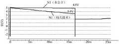
如图3B所示,为本公开的实施例提供的像素电路100以及相关技术提供的驱动电路中,驱动晶体管Td的栅极在一帧时间内的电压的模拟结果图。由图3B所示,在发光阶段,相关技术提供的驱动电路的驱动晶体管Td的栅极的电压由3.4V变为2.2V,电压变化量△V达到1.2V。本公开实施例提供的像素电路100的驱动晶体管Td的栅极的电压由3.6V变为2.9V,电压变化量△V仅为0.7V。由此可知,本公开实施例提供的像素电路100能够有效保持驱动晶体管Td的栅极电压,有利于改善Flicker现象。As shown in FIG. 3B , in the
本公开的一些实施例提供一种上述像素电路100的驱动方法。如图4所示,该方法包括S1-S3。Some embodiments of the present disclosure provide a driving method of the
S1、在一图像帧的初始化阶段:向第一复位信号端RE1输入第一复位信号,以使第一复位子电路20将来自初始化信号端INI的初始化信号传输至第三节点N3。向第一扫描端G1输入第一扫描信号,以使写入子电路30将第三节点N3上的初始化信号传输至第一节点N1,以对第一节点N1进行复位。S1. In the initialization stage of an image frame: input the first reset signal to the first reset signal terminal RE1, so that the
S2、在一图像帧的数据写入阶段:向第一扫描端G1输入第一扫描信号,向第二扫描端G2输入第二扫描信号,并向数据端DE输入数据信号,以使写入子电路20将数据端DE接收的数据信号写入至第一节点N1,对驱动晶体管Td进行阈值电压补偿。S2, the data writing stage of an image frame: input the first scanning signal to the first scanning end G1, input the second scanning signal to the second scanning end G2, and input the data signal to the data end DE, so that the writing sub- The
S3、在一图像帧的发光阶段:向第一使能信号端EM1输入第一使能信号,并向第二使能信号端EM2输入第二使能信号,以使发光控制子电路50将第一电压端VDD的电压信号传输至第二节点N2,并将驱动晶体管Td输出的电流传输至发光器件40,使发光器件40发光。S3. In the light-emitting stage of one image frame: input the first enable signal to the first enable signal terminal EM1, and input the second enable signal to the second enable signal terminal EM2, so that the light-emitting
在一些实施例中,像素电路100的驱动方法还包括:在一图像帧的初始化阶段,向数据端DE输入数据信号,以进行预充电,这样有利于数据信号写入。In some embodiments, the driving method of the
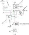
在一些实施例中,如图5所示,发光控制子电路50包括第一子电路51和第二子电路52。In some embodiments, as shown in FIG. 5 , the
第一子电路51连接第二节点N2、第一电压端VDD和第一使能信号端EM1。The
第一子电路51被配置为在发光阶段,在第一使能信号端EM1的第一使能信号的控制下,将第一电压端VDD的电压信号传输至第二节点N2。The
第二子电路52连接第三节点N3、第二使能信号端EM2和发光器件40的阳极。The
第二子电路52被配置为在发光阶段,在第二使能信号端EM2的第二使能信号的控制下,将驱动晶体管Td输出的电流传输至发光器件40。The
在一些实施例中,如图5所示,写入子电路30包括第三子电路31和第四子电路32。In some embodiments, as shown in FIG. 5 , the
第三子电路31连接第二扫描端G2、数据端DE和第二节点N2。The
第三子电路31被配置为在第二扫描端G2的第二扫描信号的控制下,至少在数据写入阶段开启,将数据端DE接收的数据信号传输至第二节点N2。The
第四子电路32连接第一扫描端G1、第一节点N1和第三节点N3。The
第四子电路32被配置为在第一扫描端G1接收的第一扫描信号的控制下,在初始化阶段和数据写入阶段开启,并在初始化阶段将第三节点N3上的初始化信号传输至第一节点N1,在数据写入阶段将第二节点N2的数据信号写入至第一节点N1并对驱动晶体管Td进行阈值电压补偿。The
以显示面板上的2×2个阵列排布的亚像素区P为例。在一些实施例中,如图6A所示,显示面板还包括多条第一扫描线GL1、多条第二扫描线GL2、多条第一使能信号线EML1、多条第二使能信号线EML2和多条第一复位信号线RL1。Take the sub-pixel regions P arranged in a 2×2 array as an example. In some embodiments, as shown in FIG. 6A , the display panel further includes a plurality of first scan lines GL1 , a plurality of second scan lines GL2 , a plurality of first enable signal lines EML1 , and a plurality of second enable signal lines EML2 and a plurality of first reset signal lines RL1.
位于同一行的所有像素电路100连接的第一扫描端G1和第二扫描端G2分别连接第一扫描线GL1和第二扫描线GL2。位于同一行的所有像素电路100连接的第一复位信号端RE1连接同一条第一复位信号线RL1。位于同一行的所有像素电路100连接的第一使能信号端EM1连接同一条第一使能信号线EML1。位于同一行的所有像素电路100连接的第二使能信号端EM2连接同一条第二使能信号线EML2。The first scan end G1 and the second scan end G2 connected to all the
第一扫描线GL1被配置为向一行像素电路100连接的第一扫描端G1提供第一扫描信号。第二扫描线GL2被配置为向一行像素电路100连接的第二扫描端G2提供第二扫描信号。第一复位信号线RL1被配置为向一行像素电路100连接的第一复位信号端RE1提供第一复位信号。第一使能信号线EML1被配置为向一行像素电路100连接的第一使能信号端EM1提供第一使能信号。第二使能信号线EML2被配置为向一行像素电路100连接的第二使能信号端EM2提供第二使能信号。The first scan line GL1 is configured to supply the first scan signal to the first scan terminal G1 to which the
如图6A所示,显示面板还包括多条数据信号线DL和多条初始化信号线IL。As shown in FIG. 6A , the display panel further includes a plurality of data signal lines DL and a plurality of initialization signal lines IL.
在一些实施例中,位于同一列的所有像素电路100连接的数据端DE连接同一条数据信号线DL。位于同一列的所有像素电路100连接的初始化信号端INI连接同一条初始化信号线IL。In some embodiments, the data terminals DE connected to all
数据信号线DL被配置为向一列像素电路100连接的数据端DE提供数据信号。初始化信号线IL被配置为向一列像素电路100连接的初始化信号端INI提供初始化信号。The data signal lines DL are configured to supply data signals to the data terminals DE to which the
在一些实施例中,第一扫描端G1和第二扫描端G2连接同一扫描端。在第一扫描端G1和第二扫描端G2连接同一扫描端的情况下,第一扫描信号和第二扫描信号为相同的扫描信号。In some embodiments, the first scan end G1 and the second scan end G2 are connected to the same scan end. In the case where the first scan end G1 and the second scan end G2 are connected to the same scan end, the first scan signal and the second scan signal are the same scan signal.
示例地,如图6B所示,显示面板包括多条扫描线GL,位于同一行的所有像素电路100连接的第一扫描端G1和第二扫描端G2均连接一条扫描线GL。即,位于同一行的所有像素电路100连接的扫描端G连接一根扫描线GL。For example, as shown in FIG. 6B , the display panel includes a plurality of scan lines GL, and one scan line GL is connected to the first scan end G1 and the second scan end G2 connected to all the
在此情况下,第三子电路31被配置为在第二扫描端G2的第二扫描信号的控制下,在初始化阶段和数据写入阶段均开启。In this case, the
在一些实施例中,第一使能信号端EM1和第二使能信号端EM2连接同一使能信号端。在第一使能信号端EM1和第二使能信号端EM2连接同一使能信号端的情况下,第一使能信号和第二使能信号为相同的使能信号。In some embodiments, the first enable signal terminal EM1 and the second enable signal terminal EM2 are connected to the same enable signal terminal. In the case where the first enable signal terminal EM1 and the second enable signal terminal EM2 are connected to the same enable signal terminal, the first enable signal and the second enable signal are the same enable signal.
示例地,如图6C所示,显示面板包括多条使能信号线EML,位于同一行的所有像素电路100连接的第一使能信号端EM1和第二使能信号端EM2连接一条使能信号线EML。即,位于同一行的所有像素电路100连接的使能信号端EM连接一条使能信号线EML。For example, as shown in FIG. 6C , the display panel includes a plurality of enable signal lines EML, and the first enable signal terminal EM1 and the second enable signal terminal EM2 connected to all the
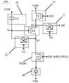
在一些示例中,如图7所示,第一复位子电路20包括第一晶体管T1,第一晶体管T1的栅极连接第一复位信号端RE1,第一晶体管T1的第一极连接初始化信号端INI,第一晶体管T1的第二极连接第三节点N3。In some examples, as shown in FIG. 7 , the
在另一些示例中,第一复位子电路20包括并联或串联的多个第一晶体管T1。在第一复位子电路20包括并联的多个第一晶体管T1的情况下,该多个第一晶体管T1的栅极均连接第一复位信号端RE1,该多个第一晶体管T1的第一极均连接初始化信号端INI,该多个第一晶体管T1的第二极均连接第三节点N3。在第一复位子电路20包括串联的多个第一晶体管T1的情况下,该多个第一晶体管T1依次连接(第一个第一晶体管T1的第二极连接第二个第一晶体管T1的第一极,依次类推),该多个第一晶体管T1的栅极均连接第一复位信号端RE1,该多个第一晶体管T1中的第一个第一晶体管T1的第一极连接初始化信号端INI,最后一个第一晶体管T1的第二极连接第三节点N3。上述仅仅是对第一复位子电路20的举例说明,其它与该第一复位子电路20功能相同的结构在此不再一一赘述,但都应当属于本公开的保护范围。In other examples, the
在一些示例中,如图7所示,第一子电路51包括第三晶体管T3,第三晶体管T3的栅极连接第一使能信号端EM1,第三晶体管T3的第一极连接第一电压端VDD,第三晶体管T3的第二极连接第二节点N2。In some examples, as shown in FIG. 7 , the
在另一些示例中,第一子电路51包括并联或串联的多个第三晶体管T3。在第一子电路51包括并联的多个第三晶体管T3的情况下,该多个第三晶体管T3的栅极均连接第一使能信号端EM1,该多个第三晶体管T3的第一极均连接第一电压端VDD,该多个第三晶体管T3的第二极均连接第二节点N2。在第一子电路51包括串联的多个第三晶体管T3的情况下,该多个第三晶体管T3依次连接(第一个第三晶体管T3的第二极连接第二个第三晶体管T3的第一极,依次类推),该多个第三晶体管T3的栅极均连接第一使能信号端EM1,该多个第三晶体管T3中的第一个第三晶体管T3的第一极连接第一电压端VDD,最后一个第三晶体管T1的第二极连接第二节点N2。上述仅仅是对第一子电路51的举例说明,其它与该第一子电路51功能相同的结构在此不再一一赘述,但都应当属于本公开的保护范围。In other examples, the
在一些示例中,如图7所示,第二子电路52包括第四晶体管T4,第四晶体管T4的栅极连接第二使能信号端EM2,第四晶体管T4的第一极连接第三节点N3,第四晶体管T4的第二极连接发光器件40的阳极。In some examples, as shown in FIG. 7 , the
在另一些示例中,第二子电路52包括并联或串联的多个第四晶体管T4。在第二子电路52包括并联的多个第四晶体管T4的情况下,该多个第四晶体管T4的栅极均连接第二使能信号端EM2,该多个第四晶体管T4的第一极均连接第三节点N3,该多个第四晶体管T4的第二极均连接发光器件40的阳极。在第二子电路52包括串联的多个第四晶体管T4的情况下,该多个第四晶体管T4依次连接(第一个第四晶体管T4的第二极连接第二个第四晶体管T4的第一极,依次类推),该多个第四晶体管T4的栅极均连接第二使能信号端EM2,该多个第四晶体管T4中的第一个第四晶体管T4的第一极连接第三节点N3,最后一个第四晶体管T4的第二极连接发光器件40的阳极。上述仅仅是对第二子电路52的举例说明,其它与该第二子电路52功能相同的结构在此不再一一赘述,但都应当属于本公开的保护范围。In other examples, the
在一些示例中,如图7所示,第三子电路31包括第五晶体管T5,第五晶体管T5的栅极连接第二扫描端G2,第五晶体管T5的第一极连接数据端DE,第五晶体管T5的第二极连接第二节点N2。In some examples, as shown in FIG. 7 , the
在另一些示例中,第三子电路31包括并联或串联的多个第五晶体管T5。在第三子电路31包括并联的多个第五晶体管T5的情况下,该多个第五晶体管T5的栅极均连接第二扫描端G2,该多个第五晶体管T5的第一极均连接数据端DE,该多个第五晶体管T5的第二极均连接第二节点N2。在第三子电路31包括串联的多个第五晶体管T5的情况下,该多个第五晶体管T5依次连接(第一个第五晶体管T5的第二极连接第二个第五晶体管T5的第一极,依次类推),该多个第五晶体管T5的栅极均连接第二扫描端G2,该多个第五晶体管T5中的第一个第五晶体管T5的第一极连接数据端DE,最后一个第五晶体管T5的第二极连接第二节点N2。上述仅仅是对第三子电路31的举例说明,其它与该第三子电路31功能相同的结构在此不再一一赘述,但都应当属于本公开的保护范围。In other examples, the
在一些示例中,如图7所示,第四子电路32包括第六晶体管T6,第六晶体管T6的栅极连接第一扫描端G1,第六晶体管T6的第一极连接第三节点N3,第六晶体管T6的第二极连接第一节点N1。In some examples, as shown in FIG. 7 , the
在另一些示例中,第四子电路32包括并联或串联的多个第六晶体管T6。在第四子电路32包括并联的多个第六晶体管T6的情况下,该多个第六晶体管T6的栅极均连接第一扫描端G1,该多个第六晶体管T6的第一极均连接第三节点N3,该多个第六晶体管T6的第二极均连接第一节点N1。在第四子电路32包括串联的多个第六晶体管T6的情况下,该多个第六晶体管T6依次连接(第一个第六晶体管T6的第二极连接第二个第六晶体管T6的第一极,依次类推),该多个第六晶体管T6的栅极均连接第一扫描端G1,该多个第六晶体管T6中的第一个第六晶体管T6的第一极连接第三节点N3,最后一个第六晶体管T6的第二极连接第一节点N1。上述仅仅是对第四子电路32的举例说明,其它与该第四子电路32功能相同的结构在此不再一一赘述,但都应当属于本公开的保护范围。In other examples, the
需要说明的是,本公开实施例对各个子电路中的晶体管的类型不做限定,即上述驱动晶体管Td、第一晶体管T1、第三晶体管T3、第四晶体管T4以及第五晶体管T5、第六晶体管T6可以均为P型晶体管或者均为N型晶体管。以下以上述驱动晶体管Td、第一晶体管T1、第三晶体管T3、第四晶体管T4以及第五晶体管T5、第六晶体管T6均为P型晶体管进行说明。It should be noted that the embodiments of the present disclosure do not limit the types of transistors in each sub-circuit, that is, the above-mentioned driving transistor Td, first transistor T1, third transistor T3, fourth transistor T4, fifth transistor T5, sixth transistor The transistors T6 may all be P-type transistors or all N-type transistors. In the following, the above-mentioned driving transistor Td, the first transistor T1, the third transistor T3, the fourth transistor T4, the fifth transistor T5, and the sixth transistor T6 are all P-type transistors for description.
此外,第一极为晶体管的源极和漏极中一者,第二极为晶体管的源极和漏极中另一者。由于晶体管的源极、漏极在结构上可以是对称的,所以其源极、漏极在结构上可以是没有区别的,也就是说,本公开的实施例中的晶体管的第一极和第二极在结构上可以是没有区别的。对于P型驱动晶体管Td,通常将第二极称为漏极,将第一极称为源极;对于N型驱动晶体管Td,通常将第一极称为漏极,将第二极称为源极。In addition, the first pole is one of the source and the drain of the transistor, and the second pole is the other of the source and the drain of the transistor. Since the source and drain of the transistor may be symmetrical in structure, the source and drain of the transistor may be indistinguishable in structure, that is, the first electrode and the second electrode of the transistor in the embodiments of the present disclosure Diodes may be indistinguishable in structure. For the P-type driving transistor Td, the second electrode is usually called the drain electrode, and the first electrode is called the source electrode; for the N-type driving transistor Td, the first electrode is usually called the drain electrode, and the second electrode is called the source electrode. pole.
下面提供几种可能的实施方式,以对像素电路100及其驱动过程,进行说明。Several possible implementation manners are provided below to describe the
像素电路100在一图像帧的驱动过程可以分为初始化阶段P1、数据写入阶段P2和发光阶段P3。The driving process of the
第一种可能的实施方式:First possible implementation:
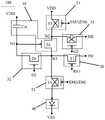
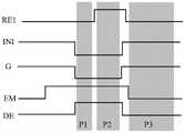
如图7所示,第一复位子电路20包括第一晶体管T1,第一子电路51包括第三晶体管T3,第二子电路52包括第四晶体管T4,第三子电路31包括第五晶体管T5,第四子电路32包括第六晶体管T6。第一使能信号端EM1和第二使能信号端EM2连接同一使能信号端EM。As shown in FIG. 7 , the
如图8所示,在初始化阶段P1:第一复位信号端RE1输出的第一复位信号和第一扫描端G1输出的第一扫描信号的电位为低电平,使能信号端EM输出的使能信号以及第二扫描端G2输出的第二扫描信号的电位为高电平。As shown in FIG. 8 , in the initialization stage P1: the potential of the first reset signal output by the first reset signal terminal RE1 and the first scan signal output by the first scanning terminal G1 is low, and the enable signal output by the enable signal terminal EM The potentials of the enable signal and the second scan signal output from the second scan terminal G2 are at a high level.
图7中第一复位子电路20在第一复位信号的控制下,将来自初始化信号端INI的初始化信号传输至第三节点N3。第四子电路32在第一扫描信号的控制下,将第三节点N3上的初始化信号传输至第一节点N1,以通过初始化信号对第一节点N1进行初始化,避免上一帧残留于第一节点N1的电信号对本帧画面造成影响。In FIG. 7 , the
如图9A(为图7所示的像素电路100在初始化阶段P1的等效电路图)所示,第一复位信号控制第一晶体管T1开启,初始化信号端INI输入的初始化信号经第一晶体管T1传输至第三节点N3。第一扫描信号控制第六晶体管T6开启,初始化信号经第六晶体管T6传输至第一节点N1。As shown in FIG. 9A (the equivalent circuit diagram of the
此外,第一子电路51、第二子电路52和第三子电路31在初始化阶段P1均处于关闭状态。在此情况下,如图9A所示,第三晶体管T3、第四晶体管T4和第五晶体管T5均截止。如图9A所示,处于截止状态的晶体管以打“×”表示。In addition, the
在初始化阶段P1结束时,第一节点N1的电位为Vinit。At the end of the initialization phase P1, the potential of the first node N1 is Vinit .
数据写入阶段P2:第一扫描端G1输出的第一扫描信号和第二扫描端G2输出的第二扫描信号的电位为低电平,第一复位信号端RE1输出的第一复位信号以及使能信号端EM输出的使能信号的电位为高电平。Data writing stage P2: the potentials of the first scan signal output by the first scan terminal G1 and the second scan signal output by the second scan terminal G2 are low levels, the first reset signal output by the first reset signal terminal RE1 and the The potential of the enable signal output by the enable signal terminal EM is a high level.
图7中第三子电路31在第二扫描信号的控制下,将来自数据端DE的数据信号传输至第二节点N2。第四子电路32在第一扫描信号的控制下,将驱动晶体管Td的第二极和栅极短接,形成二极管结构,将第二节点N2上的数据信号写入至第一节点N1,并对驱动晶体管Td进行阈值电压补偿。The third sub-circuit 31 in FIG. 7 transmits the data signal from the data terminal DE to the second node N2 under the control of the second scan signal. Under the control of the first scan signal, the fourth sub-circuit 32 short-circuits the second pole and the gate of the driving transistor Td to form a diode structure, writes the data signal on the second node N2 to the first node N1, and Threshold voltage compensation is performed on the drive transistor Td.
如图9B(为图7所示的像素电路100在数据写入阶段P2的等效电路图)所示,在数据写入阶段P2,第一复位信号的电位为高电平,第一晶体管T1截止。第二扫描信号的电位为低电平,控制第五晶体管T5开启,来自数据端DE的数据信号经第五晶体管T5传输至第二节点N2。与初始化阶段P1相同,在数据写入阶段P2,第一扫描信号的电位仍为低电平,第六晶体管T6保持开启,将驱动晶体管Td的第二极和栅极短接,形成二极管结构,第二节点N2上的数据信号通过驱动晶体管Td和第六晶体管T6传输至第一节点N1。当第一节点N1的电位与第二节点N2的电位的压差减小至驱动晶体管Td的阈值电压Vth时,驱动晶体管Td截至。As shown in FIG. 9B (the equivalent circuit diagram of the
在数据写入阶段P2结束时,第一节点N1的电位为Vdata+Vth,并将该电位存储于存储电容Cst中。When the data writing phase P2 ends, the potential of the first node N1 is Vdata +Vth, and the potential is stored in the storage capacitor Cst.
发光阶段P3:使能信号端EM输出的使能信号的电位为低电平,第一扫描端G1输出的第一扫描信号的电位、第二扫描端G2输出的第二扫描信号的电位和第一复位信号端RE1输出的第一复位信号的电位均为高电平。Light-emitting stage P3: the potential of the enable signal output by the enable signal terminal EM is a low level, the potential of the first scan signal output by the first scan terminal G1, the potential of the second scan signal output by the second scan terminal G2, and the first scan signal. The potential of the first reset signal output by a reset signal terminal RE1 is all high level.
图7中第一子电路51在使能信号的控制下,将第一电压端VDD的电压信号传输至第二节点N2。驱动晶体管Td在第一节点N1的电压和第一电压端VDD的电压信号的控制下,产生驱动电流。第二子电路52在使能信号的控制下,将驱动晶体管Td输出的驱动电流,传输至发光器件40。In FIG. 7 , the first sub-circuit 51 transmits the voltage signal of the first voltage terminal VDD to the second node N2 under the control of the enable signal. The driving transistor Td generates a driving current under the control of the voltage of the first node N1 and the voltage signal of the first voltage terminal VDD. The second sub-circuit 52 transmits the driving current output by the driving transistor Td to the
如图9C(为图7所示的像素电路100在数据发光阶段P3的等效电路图)所示,第一复位信号的电位为高电平,第一晶体管T1截止。第一扫描信号的电位为高电平,第六晶体管T6截止。第二扫描信号的电位为高电平,第五晶体管T5截止。使能信号的电位为低电平,第三晶体管T3和第四晶体管T4开启。第一电压端VDD的电压信号经过第三晶体管T3传输至第二节点N2。驱动晶体管Td在第一节点N1的电压和第一电压端VDD的电压信号的控制下,产生驱动电流。驱动电流经第四晶体管T4传输至发光器件40,使发光器件40进行发光。As shown in FIG. 9C (which is an equivalent circuit diagram of the
在发光阶段P3,第一节点N1的电位为Vdata+Vth,第二节点N2的电位为Vdd,驱动晶体管Td的Vgs=Vg-Vs=Vdata+Vth-Vdd。In the light-emitting stage P3, the potential of the first node N1 isVdata +Vth, the potential of the second node N2 is Vdd, and the driving transistor Td has Vgs=Vg-Vs=Vdata +Vth-Vdd.
驱动晶体管Td开启后,当驱动晶体管Td的栅-源电压Vgs减去驱动晶体管Td的阈值电压Vth得到的值小于等于驱动晶体管Td的漏-源电压Vds时,即Vgs-Vth≤Vds时,驱动晶体管Td能够处于饱和开启状态,此时流过驱动晶体管Td的驱动电流I为:After the driving transistor Td is turned on, when the value obtained by subtracting the threshold voltage Vth of the driving transistor Td from the gate-source voltage Vgs of the driving transistor Td is less than or equal to the drain-source voltage Vds of the driving transistor Td, that is, when Vgs-Vth≤Vds, the driving The transistor Td can be in a saturated ON state, and the driving current I flowing through the driving transistor Td at this time is:

其中,W/L为驱动晶体管Td的宽长比,Cox为沟道绝缘层的介电常数,μ为沟道载流子迁移率。Wherein, W/L is the width-length ratio of the driving transistor Td, Cox is the dielectric constant of the channel insulating layer, and μ is the channel carrier mobility.
上述参数只与驱动晶体管Td的结构、数据电压端DE输出的数据信号和第一电压端VDD输出的电压信号有关,与驱动晶体管Td的阈值电压Vth无关,从而消除了驱动晶体管Td的阈值电压Vth对发光器件40的发光亮度的影响,从而可提高显示面板的亮度均一性。The above parameters are only related to the structure of the driving transistor Td, the data signal output by the data voltage terminal DE, and the voltage signal output by the first voltage terminal VDD, and have nothing to do with the threshold voltage Vth of the driving transistor Td, thus eliminating the threshold voltage Vth of the driving transistor Td. The effect on the luminous brightness of the
第二种可能的实施方式:Second possible implementation:
如图10所示,在第一种可能的实施方式基础上,第一扫描端G1和第二扫描端G2连接同一扫描端G。基于此,图10所示的像素电路100的时序控制图如图11所示。As shown in FIG. 10 , on the basis of the first possible implementation manner, the first scanning end G1 and the second scanning end G2 are connected to the same scanning end G. Based on this, the timing control diagram of the
如图11所示,在初始化阶段P1:第一复位信号端RE1输出的第一复位信号的电位和扫描端G输出的扫描信号的电位为低电平,使能信号端EM输出的使能信号的电位为高电平。As shown in FIG. 11 , in the initialization stage P1: the potential of the first reset signal output by the first reset signal terminal RE1 and the potential of the scan signal output by the scan terminal G are low levels, and the enable signal output by the enable signal terminal EM potential is high.
如图12A(为图10所示的像素电路100在初始化阶段P1的等效电路图)所示,在初始化阶段P1,第一复位信号的电位为低电平,控制第一晶体管T1开启,初始化信号端INI输入的初始化信号经第一晶体管T1传输至第三节点N3。扫描信号的电位为低电平,第六晶体管T6开启,初始化信号经第六晶体管T6传输至第一节点N1。As shown in FIG. 12A (which is the equivalent circuit diagram of the
此外,使能信号的电位在初始化阶段P1为高电平,第一子电路51和第二子电路52处于关闭状态。如图11和图12A所示,第三晶体管T3和第四晶体管T4截止。In addition, the potential of the enable signal is at a high level in the initialization phase P1, and the
如图11所示,在数据写入阶段P2:扫描端G输出的扫描信号的电位为低电平,第一复位信号端RE1输出的第一复位信号的电位、使能信号端EM输出的使能信号的电位为高电平。As shown in FIG. 11 , in the data writing phase P2: the potential of the scan signal output by the scan terminal G is at a low level, the potential of the first reset signal output by the first reset signal terminal RE1, and the enable signal output by the enable signal terminal EM The potential of the energy signal is a high level.
如图12B(为图10所示的像素电路100在初始化阶段P2的等效电路图)所示,在数据写入阶段P2,第一复位信号的电位为高电平,第一晶体管T1截止。扫描信号的电位为低电平,控制第五晶体管T5和第六晶体管T6开启,来自数据端DE的数据信号经第五晶体管T5传输至第二节点N2。第六晶体管T6开启,将驱动晶体管Td的第二极和栅极短接,形成二极管结构,第二节点N2上的数据信号通过驱动晶体管Td和第六晶体管T6传输至第一节点N1。当第一节点N1的电位与第二节点N2的电位的压差减小至驱动晶体管Td的阈值电压Vth时,驱动晶体管Td截至。As shown in FIG. 12B (the equivalent circuit diagram of the
发光阶段P3,各晶体管的开启状态以及信号的传输过程,与第一种可能的实施方式中发光阶段P3相同,此处不再赘述。In the light-emitting stage P3, the turn-on states of the transistors and the signal transmission process are the same as those in the light-emitting stage P3 in the first possible implementation manner, and are not repeated here.
需要说明的是,在第二种可能的实施方式中,在初始化阶段P1,由于扫描信号的电位为低电平,第五晶体管T5也处于开启状态,数据端DE也会输入数据信号,但是由于数据端DE和第一节点N1的电压压差小于数据端DE和初始化信号端INI的电压压差,并且数据端DE的数据信号传输到第一节点N1需要经过第五晶体管T5、驱动晶体管Td和第六晶体管T6,因此在初始化阶段P1,数据信号对第一节点N1的电压的影响较小。It should be noted that, in the second possible implementation manner, in the initialization stage P1, since the potential of the scan signal is at a low level, the fifth transistor T5 is also in an on state, and a data signal is also input to the data terminal DE. The voltage difference between the data terminal DE and the first node N1 is smaller than the voltage difference between the data terminal DE and the initialization signal terminal INI, and the data signal of the data terminal DE is transmitted to the first node N1 through the fifth transistor T5, the driving transistor Td and the The sixth transistor T6, so in the initialization phase P1, the data signal has less influence on the voltage of the first node N1.
如图13所示,为第二种可能的实施方式的像素电路100在一图像帧的驱动过程中,各信号的模拟结果。由图13可见,第一节点N1能够进行正常的初始化和数据信号的写入。As shown in FIG. 13 , it is the simulation result of each signal in the driving process of an image frame of the
第三种可能的实施方式:Third possible implementation:
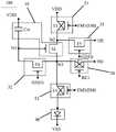
如图14所示,位于同一行的所有像素电路连接的第一扫描端G1和第二扫描端G2均连接一条扫描线GL,位于第n行的所有像素电路100连接的第一复位信号端RE1(n)连接与第n-1行像素电路100连接的扫描线GL(n-1)。在此情况下,该像素电路100对应的时序控制图如图15所示,其驱动过程与上述第二种可能的实施方式相似,此处不再赘述。所不同的是,在第三种可能的实施方式中,在初始化阶段P1,与第n行像素电路100连接的第一复位信号端RE1(n)的第一复位信号由第n-1行的扫描线GL(n-1)提供。此处,n为大于等于2的正整数。As shown in FIG. 14 , the first scan terminal G1 and the second scan terminal G2 connected to all pixel circuits in the same row are connected to a scan line GL, and the first reset signal terminal RE1 of all
位于第n行的所有像素电路100连接的第一复位信号端RE1(n)连接与第n-1行像素电路100对应的扫描线GL(n-1),不用单独设置第一复位信号线RL1,可以减少显示面板的布线数量。The first reset signal terminal RE1(n) connected to all
第四种可能的实施方式:Fourth possible implementation:
如图16所示,初始化信号端INI与发光器件40的阳极连接。在此情况下,可用发光器件40的阳极的残留电压对第一节点N1进行复位,从而可以减少显示面板上的布线数量。As shown in FIG. 16 , the initialization signal terminal INI is connected to the anode of the
示例地,像素电路100的结构如图17所示,对应的时序控制图如图18所示,该像素电路100的驱动过程与上述第一种可能的实施方式中相似。所不同的是,在第四种可能的实施方式中,在初始化阶段P1,利用发光器件40的阳极的残留电压对第一节点N1进行复位。For example, the structure of the
如图19所示,为本公开第四种可能的实施方式的像素电路100在一图像帧的驱动过程中,各信号的模拟结果。由图19可见,第一节点N1能够进行正常的初始化和数据信号的写入。As shown in FIG. 19 , the simulation results of each signal during the driving process of an image frame of the
第五种可能的实施方式:Fifth possible implementation:
如图20所示,第二子电路52与第一复位子电路20复用,第一复位信号端RE1与第二使能信号端EM2为同一信号端EM_S。As shown in FIG. 20 , the
该信号端EM_S被配置在初始化阶段P1输出第一复位信号,在发光阶段P3输出第二使能信号。The signal terminal EM_S is configured to output the first reset signal in the initialization phase P1, and output the second enable signal in the light-emitting phase P3.
示例地,像素电路100的结构如图21所示,对应的时序控制图如图22所示。该像素电路100的驱动过程如下。For example, the structure of the
如图22所示,信号端EM_S输出控制信号,该控制信号包括第一复位信号和第二使能信号。第一扫描端G1输出第一扫描信号,第二扫描端G2输出第二扫描信号。第一使能信号端EM1输出第一使能信号。As shown in FIG. 22 , the signal terminal EM_S outputs a control signal, and the control signal includes a first reset signal and a second enable signal. The first scan end G1 outputs a first scan signal, and the second scan end G2 outputs a second scan signal. The first enable signal terminal EM1 outputs a first enable signal.
在初始化阶段P1:第一复位信号的电位为低电平。第一扫描信号的电位为低电平。第一使能信号和第二扫描信号的电位均为高电平。In the initialization phase P1: the potential of the first reset signal is at a low level. The potential of the first scan signal is a low level. The potentials of the first enable signal and the second scan signal are both at a high level.
如图23A(为图21所示的像素电路100在初始化阶段P1的等效电路图)所示,在初始化阶段P1,第一复位信号的电位为低电平,控制第四晶体管T4开启,发光器件40的阳极电压经第四晶体管T4传输至第三节点N3。第一扫描信号的电位为低电平开启信号,第六晶体管T6开启,第三节点N3的电压经第六晶体管T6传输至第一节点N1,从而对第一节点N1进行复位。As shown in FIG. 23A (the equivalent circuit diagram of the
第一子电路51和第三子电路31在初始化阶段P1处于关闭状态。在此情况下,如图23A所示,第三晶体管T3和第五晶体管T5截止。The
数据写入阶段P2:第一扫描信号和第二扫描信号的电位为低电平。控制信号的电位为高电平。第一使能信号的电位为高电平。Data writing phase P2: the potentials of the first scan signal and the second scan signal are at a low level. The potential of the control signal is a high level. The potential of the first enable signal is a high level.
如图23B(为图21所示的像素电路100在数据写入阶段P2的等效电路图)所示,在数据写入阶段P2,控制信号的电位为高电平,第四晶体管T4截止。第二扫描信号的电位为低电平,控制第五晶体管T5开启,来自数据端DE的数据信号经第五晶体管T5传输至第二节点N2。与初始化阶段P1相同,在数据写入阶段P2中,第一扫描信号的电位仍为低电平,第六晶体管T6保持开启,将驱动晶体管Td的第二极和栅极短接,形成二极管结构,第二节点N2上的数据信号通过驱动晶体管Td和第六晶体管T6传输至第一节点N1。当第一节点N1的电位与第二节点N2的电位的压差减小至驱动晶体管Td的阈值电压Vth时,驱动晶体管Td截至。As shown in FIG. 23B (an equivalent circuit diagram of the
发光阶段P3:第一使能信号的电位为低电平。第二使能信号的电位为低电平。第一扫描信号、第二扫描信号的电位为高电平。Light-emitting stage P3: the potential of the first enable signal is at a low level. The potential of the second enable signal is a low level. The potentials of the first scan signal and the second scan signal are at a high level.
如图23C(为图21所示的像素电路100在数据发光阶段P3的等效电路图)所示,在发光阶段P3,第一扫描信号的电位为高电平,第六晶体管T6截止。第二扫描信号的电位为高电平,第五晶体管T5截止。第一使能信号的电位和第二使能信号的电位均为低电平,第三晶体管T3和第四晶体管T4开启。第一电压端VDD的电压信号经过第三晶体管T3传输至第二节点N2。驱动晶体管Td在第一节点N1和第一电压端VDD的电压信号的控制下,产生驱动电流。驱动电流经第四晶体管T4传输至发光器件40,使发光器件40进行发光。As shown in FIG. 23C (an equivalent circuit diagram of the
将第二子电路52与第一复位子电路20复用,从而可减少至少一个晶体管,进一步简化像素电路100。The
如图24所示,为本公开第五种可能的实施方式的像素电路100在一图像帧的驱动过程中,各信号的模拟结果。由图24可见,第一节点N1能够进行正常的初始化和数据信号的写入。As shown in FIG. 24 , the simulation results of each signal during the driving process of an image frame of the
第六种可能的实施方式:Sixth possible implementation:
如图25所示,第四子电路32包括第七晶体管T7和第八晶体管T8。As shown in FIG. 25, the
第七晶体管T7的栅极与第一扫描端G1连接,第七晶体管T7的第一极与第三节点N3连接,第七晶体管T7的第二极与第四节点N4连接。第八晶体管T8的栅极与第一扫描端G1连接,第八晶体管T8的第一极与第四节点N4连接,第八晶体管T8的第二极与第一节点N1连接。The gate of the seventh transistor T7 is connected to the first scanning terminal G1, the first pole of the seventh transistor T7 is connected to the third node N3, and the second pole of the seventh transistor T7 is connected to the fourth node N4. The gate of the eighth transistor T8 is connected to the first scanning terminal G1, the first pole of the eighth transistor T8 is connected to the fourth node N4, and the second pole of the eighth transistor T8 is connected to the first node N1.
在此基础上,如图25所示,第一复位子电路20包括第九晶体管T9和上述第七晶体管T7。On this basis, as shown in FIG. 25 , the
第九晶体管T9的栅极与第一复位信号端RE1连接,第九晶体管T9的第一极与初始化信号端INI连接,第九晶体管T9的第二极与第四节点N4连接。The gate of the ninth transistor T9 is connected to the first reset signal terminal RE1, the first pole of the ninth transistor T9 is connected to the initialization signal terminal INI, and the second pole of the ninth transistor T9 is connected to the fourth node N4.
第一子电路51、第二子电路52、第三子电路31的结构可参考第一种可能实施方式中第一子电路51、第二子电路52、第三子电路31,在此不再赘述。For the structures of the
第一扫描端G1和第二扫描端G2连接同一扫描端G。第一使能信号端EM1和第二使能信号端EM2连接同一使能信号端EM。The first scanning end G1 and the second scanning end G2 are connected to the same scanning end G. The first enable signal terminal EM1 and the second enable signal terminal EM2 are connected to the same enable signal terminal EM.
该像素电路100对应的时序控制图如图26所示。第一复位信号端RE1输出第一复位信号,扫描端G输出的扫描信号,使能信号端EM输出使能信号,初始化信号端INI输出初始化信号。The timing control diagram corresponding to the
初始化阶段P1:第一复位信号的电位和扫描信号的电位为低电平,使能信号的电位为高电平。Initialization stage P1: the potential of the first reset signal and the potential of the scan signal are at a low level, and the potential of the enable signal is at a high level.
如图27A(为图25所示的像素电路100在初始化阶段P1的等效电路图)所示,在初始化阶段P1,第一复位信号的电位为低电平,控制第九晶体管T9开启。初始化信号端INI输出的初始化信号经第九晶体管T9传输至第四节点N4。示例的,在初始化阶段P1,初始化信号的电位为第一电平,例如为-2.5V。扫描信号的电位为低电平,第七晶体管T7和第八晶体管T8开启,第一电平经第七晶体管T7和第八晶体管T8分别传输至第一节点N1和第三节点N3。As shown in FIG. 27A (an equivalent circuit diagram of the
在初始化阶段P1,使能信号的电位为高电平,第三晶体管T3和第四晶体管T4截止。In the initialization phase P1, the potential of the enable signal is at a high level, and the third transistor T3 and the fourth transistor T4 are turned off.
示例地,在初始化阶段P1,数据端DE也可以输入数据信号,以进行预充电,有利于数据信号写入。For example, in the initialization phase P1, the data terminal DE may also input a data signal to perform precharging, which is beneficial to the writing of the data signal.
数据写入阶段P2:扫描信号的电位为低电平,第一复位信号的电位和使能信号的电位为高电平。Data writing phase P2: the potential of the scan signal is at a low level, and the potential of the first reset signal and the potential of the enable signal are at a high level.
如图27B(为图25所示的像素电路100在数据写入阶段P2的等效电路图)所示,在数据写入阶段P2,第一复位信号的电位为高电平,第九晶体管T9截止。扫描信号的电位为低电平,第五晶体管T5开启,来自数据端DE的数据信号经第五晶体管T5传输至第二节点N2。第七晶体管T7和第八晶体管T8开启,使驱动晶体管Td的第二极和栅极短接,形成二极管结构,第二节点N2上的数据信号通过驱动晶体管Td、第七晶体管T7和第八晶体管T8传输至第一节点N1。当第一节点N1的电位与第二节点N2的电位的压差减小至驱动晶体管Td的阈值电压Vth时,驱动晶体管Td截至。As shown in FIG. 27B (the equivalent circuit diagram of the
发光阶段P3:第一复位信号和使能信号的电位为低电平,扫描信号的电位为高电平。Light-emitting stage P3: the potentials of the first reset signal and the enable signal are at a low level, and the potential of the scan signal is at a high level.
如图27C(为图25所示的像素电路100在数据发光阶段P3的等效电路图)所示,在发光阶段P3,第一复位信号的电位为低电平,控制第九晶体管T9开启。初始化信号的电位为第二电平,该第二电平经第九晶体管T9传输至第四节点N4。示例的,在发光阶段P3,第二电平例如为4.5V。As shown in FIG. 27C (an equivalent circuit diagram of the
扫描信号的电位为高电平,第五晶体管T5、第七晶体管T7和第八晶体管T8截止。The potential of the scan signal is at a high level, and the fifth transistor T5, the seventh transistor T7 and the eighth transistor T8 are turned off.
使能信号的电位为低电平,第三晶体管T3和第四晶体管T4开启。第一电压端VDD的电压信号经过第三晶体管T3传输至第二节点N2。驱动晶体管Td在第一节点N1的电位和第一电压端VDD的电压信号的控制下,产生驱动电流。驱动电流经第四晶体管T4传输至发光器件40,使发光器件40进行发光。The potential of the enable signal is at a low level, and the third transistor T3 and the fourth transistor T4 are turned on. The voltage signal of the first voltage terminal VDD is transmitted to the second node N2 through the third transistor T3. The driving transistor Td generates a driving current under the control of the potential of the first node N1 and the voltage signal of the first voltage terminal VDD. The driving current is transmitted to the
在该像素电路100中,在发光阶段P3,初始化信号的第二电平经第九晶体管T9传输至第四节点N4,且该第二电平为高电平,这样使第一节点N1和第四节点N4之间的压差减小,从而减小第一节点N1向第四节点N4的漏电流,进而可以更好地保持第一节点N1在一帧时间内的电压,进一步降低Flicker现象的发生几率。In the
如图28所示,为本公开第六种可能的实施方式的像素电路100在一图像帧的驱动过程中,各信号的模拟结果。由图28可见,第一节点N1能够进行正常的初始化和数据信号的写入。As shown in FIG. 28 , the simulation results of each signal during the driving process of an image frame of the
如图29所示,为本公开第六种可能的实施方式的像素电路100以及相关技术提供的像素电路100的驱动晶体管Td的栅极在一帧时间内的电压的模拟结果图。在一帧时间内,相关技术提供的像素电路100的驱动晶体管Td的栅极的电压由5V变为3.4V,电压变化量△V达到1.6V;本公开实施例提供的像素电路100的驱动晶体管Td的栅极的电压由5V变为4.9V,电压变化量△V仅为0.1V。本公开实施例提供的像素电路100能够有效保持驱动晶体管Td的栅极电压,有利于改善Flicker现象,可用于超低频率(例如1Hz)等显示面板。As shown in FIG. 29 , a simulation result diagram of the voltage of the gate of the driving transistor Td of the
第七种可能的实施方式:Seventh possible implementation:
在第一种、第二种、第三种、第六种可能的实施方式基础上,如图30A所示,像素电路100还包括第二复位子电路60,该第二复位子电路60连接发光器件40的阳极、第二复位信号端RE2和初始化信号端INI。第二复位信号端RE2被配置为接收第二复位信号,并向第二复位子电路60输出该第二复位信号。初始化信号端INI还被配置为向第二复位子电路60输出该初始化信号。On the basis of the first, second, third, and sixth possible implementation manners, as shown in FIG. 30A , the
第二复位子电路60被配置为在初始化阶段P1或数据写入阶段P2,在第二复位信号端RE2接收的第二复位信号的控制下,将来自初始化信号端INI的初始化信号传输至发光器件40的阳极,对发光器件40的阳极进行复位。The
第二复位子电路60可对发光器件40的阳极进行复位,避免在一帧画面结束时,发光器件40的阳极的残留电压对下一帧画面的影响。The second reset sub-circuit 60 can reset the anode of the light-emitting
在一些实施例中,上述第二复位信号端RE2和第一复位信号端RE1连接同一复位信号端。这样可简化像素电路100的结构。In some embodiments, the second reset signal terminal RE2 and the first reset signal terminal RE1 are connected to the same reset signal terminal. This can simplify the structure of the
需要说明的是,在第一复位信号端RE1和第二复位信号端RE2连接同一复位信号端的情况下,第一复位信号和第二复位信号为相同的复位信号。在此情况下,第二复位子电路60被配置为在初始化阶段P1,将来自初始化信号端INI的初始化信号传输至发光器件40的阳极,对发光器件40的阳极进行复位。It should be noted that, when the first reset signal terminal RE1 and the second reset signal terminal RE2 are connected to the same reset signal terminal, the first reset signal and the second reset signal are the same reset signal. In this case, the
在一些示例中,如图30B所示,第二复位子电路60包括第二晶体管T2,第二晶体管T2的栅极连接第二复位信号端RE2,第二晶体管T2的第一极连接初始化信号端INI,第二晶体管T2的第二极连接发光器件40的阳极。In some examples, as shown in FIG. 30B , the
在另一些示例中,第二复位子电路60包括并联或串联的多个第二晶体管T2。在第二复位子电路60包括并联的多个第二晶体管T2的情况下,该多个第二晶体管T2的栅极均连接第二复位信号端RE2,该多个第二晶体管T2的第一极均连接初始化信号端INI,该多个第二晶体管T2的第二极均连接发光器件40的阳极。在第二复位子电路60包括串联的多个第二晶体管T2的情况下,该多个第二晶体管T2依次连接(第一个第二晶体管T2的第二极连接第二个第二晶体管T2的第一极,依次类推),该多个第二晶体管T2的栅极均连接第二复位信号端RE2,该多个第二晶体管T2中的第一个第二晶体管T2的第一极连接初始化信号端INI,最后一个第二晶体管T2的第二极连接发光器件40的阳极。上述仅仅是对第二复位子电路60的举例说明,其它与该第二复位子电路60功能相同的结构在此不再一一赘述,但都应当属于本公开的保护范围。In other examples, the
以上所述,仅为本公开的具体实施方式,但本公开的保护范围并不局限于此,任何熟悉本技术领域的技术人员在本公开揭露的技术范围内,想到变化或替换,都应涵盖在本公开的保护范围之内。因此,本公开的保护范围应以所述权利要求的保护范围为准。The above are only specific embodiments of the present disclosure, but the protection scope of the present disclosure is not limited thereto. Any person skilled in the art who is familiar with the technical scope disclosed in the present disclosure, think of changes or replacements, should cover within the scope of protection of the present disclosure. Therefore, the protection scope of the present disclosure should be based on the protection scope of the claims.
Claims (15)
Priority Applications (4)
| Application Number | Priority Date | Filing Date | Title |
|---|---|---|---|
| CN202010479787.XACN111508426B (en) | 2020-05-29 | 2020-05-29 | Pixel circuit and driving method thereof, and display panel |
| US17/763,598US11688348B2 (en) | 2020-05-29 | 2021-04-13 | Pixel circuit and driving method thereof and display panel |
| PCT/CN2021/087044WO2021238470A1 (en) | 2020-05-29 | 2021-04-13 | Pixel circuit and driving method thereof and display panel |
| US18/320,042US12073787B2 (en) | 2020-05-29 | 2023-05-18 | Display panel |
Applications Claiming Priority (1)
| Application Number | Priority Date | Filing Date | Title |
|---|---|---|---|
| CN202010479787.XACN111508426B (en) | 2020-05-29 | 2020-05-29 | Pixel circuit and driving method thereof, and display panel |
Publications (2)
| Publication Number | Publication Date |
|---|---|
| CN111508426A CN111508426A (en) | 2020-08-07 |
| CN111508426Btrue CN111508426B (en) | 2022-04-15 |
Family
ID=71870329
Family Applications (1)
| Application Number | Title | Priority Date | Filing Date |
|---|---|---|---|
| CN202010479787.XAActiveCN111508426B (en) | 2020-05-29 | 2020-05-29 | Pixel circuit and driving method thereof, and display panel |
Country Status (3)
| Country | Link |
|---|---|
| US (1) | US11688348B2 (en) |
| CN (1) | CN111508426B (en) |
| WO (1) | WO2021238470A1 (en) |
Families Citing this family (23)
| Publication number | Priority date | Publication date | Assignee | Title |
|---|---|---|---|---|
| CN111508426B (en) | 2020-05-29 | 2022-04-15 | 京东方科技集团股份有限公司 | Pixel circuit and driving method thereof, and display panel |
| US12073787B2 (en) | 2020-05-29 | 2024-08-27 | Chengdu Boe Optoelectronics Technology Co., Ltd. | Display panel |
| CN114512086B (en)* | 2020-10-26 | 2024-02-06 | 京东方科技集团股份有限公司 | Pixel circuit, driving method thereof and electronic equipment |
| CN113112960A (en)* | 2021-04-08 | 2021-07-13 | 京东方科技集团股份有限公司 | Pixel circuit, driving method thereof and display device |
| WO2022226951A1 (en) | 2021-04-30 | 2022-11-03 | 京东方科技集团股份有限公司 | Pixel circuit and driving method therefor, and display device |
| CN113516952B (en)* | 2021-05-26 | 2022-11-18 | 京东方科技集团股份有限公司 | Pixel driving circuit, driving method thereof and display panel |
| CN115547219B (en)* | 2021-06-30 | 2023-10-24 | 荣耀终端有限公司 | Display control device, display device and electronic equipment |
| CN114514573B (en) | 2021-07-30 | 2022-08-09 | 京东方科技集团股份有限公司 | Pixel circuit, driving method and display device |
| JP2024528772A (en) | 2021-07-30 | 2024-08-01 | 京東方科技集團股▲ふん▼有限公司 | Pixel circuit, driving method thereof, and display device |
| CN113870786B (en)* | 2021-09-28 | 2023-01-10 | 京东方科技集团股份有限公司 | Pixel circuit, driving light emitting device and display device |
| CN114023266B (en)* | 2021-10-29 | 2022-12-09 | 维信诺科技股份有限公司 | Pixel circuit, display panel and display device |
| CN113889042B (en)* | 2021-11-11 | 2023-02-17 | 武汉天马微电子有限公司 | Pixel driving circuit, driving method thereof and display panel |
| CN114078430A (en)* | 2021-12-09 | 2022-02-22 | 武汉华星光电半导体显示技术有限公司 | Pixel circuit and display panel |
| CN114974130A (en)* | 2022-05-24 | 2022-08-30 | 京东方科技集团股份有限公司 | Pixel driving circuit and driving method thereof, array substrate and display device |
| CN115376451A (en)* | 2022-09-21 | 2022-11-22 | 武汉天马微电子有限公司 | Pixel circuit, driving method thereof, array substrate, display panel and display device |
| CN115527486B (en)* | 2022-10-24 | 2025-02-11 | 京东方科技集团股份有限公司 | Display substrate and display device |
| WO2024119503A1 (en)* | 2022-12-09 | 2024-06-13 | 京东方科技集团股份有限公司 | Pixel circuit and driving method therefor, and array substrate and display apparatus |
| CN116129808B (en)* | 2023-01-05 | 2025-08-15 | 京东方科技集团股份有限公司 | Display substrate, working method thereof and display device |
| CN115985232A (en)* | 2023-01-10 | 2023-04-18 | 京东方科技集团股份有限公司 | Pixel driving circuit, display panel and control method thereof |
| CN118742945A (en)* | 2023-01-19 | 2024-10-01 | 京东方科技集团股份有限公司 | Pixel circuit, display panel and display device |
| WO2024152283A1 (en)* | 2023-01-19 | 2024-07-25 | 京东方科技集团股份有限公司 | Pixel circuit, pixel driving method, and display apparatus |
| CN119132229A (en)* | 2023-06-12 | 2024-12-13 | 荣耀终端有限公司 | Voltage control method, device and storage medium |
| CN119856216B (en)* | 2023-08-17 | 2025-09-26 | 京东方科技集团股份有限公司 | Pixel driving circuit and driving method thereof, display device and signal processing method |
Family Cites Families (32)
| Publication number | Priority date | Publication date | Assignee | Title |
|---|---|---|---|---|
| KR100719924B1 (en)* | 2005-04-29 | 2007-05-18 | 비오이 하이디스 테크놀로지 주식회사 | Organic electroluminescent display |
| KR101965724B1 (en)* | 2012-10-18 | 2019-04-04 | 삼성디스플레이 주식회사 | Emitting driver for display device, display device and driving method thereof |
| CN103971638B (en)* | 2014-05-04 | 2016-03-16 | 京东方科技集团股份有限公司 | Pixel-driving circuit, driving method, array base palte and display device |
| CN104658484B (en) | 2015-03-18 | 2018-01-16 | 上海和辉光电有限公司 | Display device, pixel-driving circuit and its driving method |
| KR102559083B1 (en)* | 2015-05-28 | 2023-07-25 | 엘지디스플레이 주식회사 | Organic Light EmitPing Display |
| KR102338942B1 (en)* | 2015-06-26 | 2021-12-14 | 엘지디스플레이 주식회사 | Organic Light Emitting Display and Driving Method thereof |
| KR102457757B1 (en) | 2015-10-28 | 2022-10-24 | 삼성디스플레이 주식회사 | Pixel circuit and organic light emitting display device including the same |
| CN107731167A (en)* | 2016-08-12 | 2018-02-23 | 京东方科技集团股份有限公司 | Image element circuit, display panel, display device and driving method |
| CN106097964B (en)* | 2016-08-22 | 2018-09-18 | 京东方科技集团股份有限公司 | Pixel circuit, display panel, display equipment and driving method |
| CN106128360B (en)* | 2016-09-08 | 2018-11-13 | 京东方科技集团股份有限公司 | Pixel circuit, display panel, display equipment and driving method |
| CN106652912B (en)* | 2016-12-13 | 2020-05-19 | 上海天马有机发光显示技术有限公司 | Organic light-emitting pixel driving circuit, driving method and organic light-emitting display panel |
| CN106782313B (en)* | 2016-12-15 | 2019-04-12 | 上海天马有机发光显示技术有限公司 | Organic light emissive pixels driving circuit, driving method and organic light emitting display panel |
| CN106448555B (en)* | 2016-12-16 | 2019-11-12 | 上海天马有机发光显示技术有限公司 | Organic light emitting display panel, driving method thereof and organic light emitting display device |
| CN106710529B (en)* | 2016-12-19 | 2019-02-05 | 上海天马有机发光显示技术有限公司 | A pixel driving circuit, driving method and organic light emitting display panel |
| CN106531085B (en)* | 2017-01-05 | 2019-05-24 | 上海天马有机发光显示技术有限公司 | Organic light emitting display panel and its driving method, organic light-emitting display device |
| CN106652908B (en)* | 2017-01-05 | 2019-03-12 | 上海天马有机发光显示技术有限公司 | Organic light emitting display panel and its driving method, organic light-emitting display device |
| CN106531076B (en)* | 2017-01-12 | 2019-03-01 | 京东方科技集团股份有限公司 | A kind of pixel circuit, display panel and its driving method |
| CN106558287B (en)* | 2017-01-25 | 2019-05-07 | 上海天马有机发光显示技术有限公司 | Organic light-emitting pixel driving circuit, driving method and organic light-emitting display panel |
| CN106910468B (en)* | 2017-04-28 | 2019-05-10 | 上海天马有机发光显示技术有限公司 | The driving method of display panel, display device and pixel circuit |
| CN107424555B (en)* | 2017-05-23 | 2021-08-24 | 上海和辉光电股份有限公司 | Pixel circuit, driving method and display |
| CN107452331B (en)* | 2017-08-25 | 2023-12-05 | 京东方科技集团股份有限公司 | Pixel circuit, driving method thereof and display device |
| CN107610652B (en)* | 2017-09-28 | 2019-11-19 | 京东方科技集团股份有限公司 | Pixel circuit, driving method thereof, display panel and display device |
| CN107481676B (en)* | 2017-09-30 | 2020-09-08 | 上海天马有机发光显示技术有限公司 | Pixel circuit driving method, display panel and display device |
| CN108492777B (en)* | 2018-02-27 | 2020-04-03 | 上海天马有机发光显示技术有限公司 | Driving method of pixel driving circuit, display panel and display device |
| CN108735155A (en)* | 2018-06-01 | 2018-11-02 | 京东方科技集团股份有限公司 | A kind of pixel circuit, its driving method and display panel, display device |
| CN109087610A (en)* | 2018-08-20 | 2018-12-25 | 武汉华星光电半导体显示技术有限公司 | AMOLED pixel-driving circuit, driving method and display panel |
| WO2020107420A1 (en)* | 2018-11-30 | 2020-06-04 | Boe Technology Group Co., Ltd. | Pixel circuit, driving method, and display apparatus |
| CN110223636B (en)* | 2019-06-17 | 2021-01-15 | 京东方科技集团股份有限公司 | Pixel driving circuit, driving method thereof and display device |
| CN110299107B (en)* | 2019-06-28 | 2021-01-29 | 上海天马有机发光显示技术有限公司 | Organic light-emitting display panel and organic light-emitting display device |
| CN110310603A (en)* | 2019-07-09 | 2019-10-08 | 京东方科技集团股份有限公司 | A pixel driving circuit and its driving method, display panel, and display device |
| KR102665738B1 (en)* | 2020-05-27 | 2024-05-13 | 삼성전자주식회사 | Oled disaply system |
| CN111508426B (en) | 2020-05-29 | 2022-04-15 | 京东方科技集团股份有限公司 | Pixel circuit and driving method thereof, and display panel |
- 2020
- 2020-05-29CNCN202010479787.XApatent/CN111508426B/enactiveActive
- 2021
- 2021-04-13USUS17/763,598patent/US11688348B2/enactiveActive
- 2021-04-13WOPCT/CN2021/087044patent/WO2021238470A1/ennot_activeCeased
Also Published As
| Publication number | Publication date |
|---|---|
| US20220343852A1 (en) | 2022-10-27 |
| CN111508426A (en) | 2020-08-07 |
| US11688348B2 (en) | 2023-06-27 |
| WO2021238470A1 (en) | 2021-12-02 |
Similar Documents
| Publication | Publication Date | Title |
|---|---|---|
| CN111508426B (en) | Pixel circuit and driving method thereof, and display panel | |
| CN115691425B (en) | Pixel circuit and driving method thereof, and display panel | |
| US11270630B2 (en) | Driving circuit, driving method thereof and display apparatus | |
| US10373557B2 (en) | Organic light-emitting pixel driving circuit, driving method and organic light-emitting display panel | |
| CN107452331B (en) | Pixel circuit, driving method thereof and display device | |
| CN104157238B (en) | Image element circuit, the driving method of image element circuit and display device | |
| US10565933B2 (en) | Pixel circuit, driving method thereof, array substrate, display device | |
| KR101341788B1 (en) | Light lmitting display device and driving method thereof | |
| CN104036726B (en) | Image element circuit and driving method, OLED display panel and device | |
| CN106531074A (en) | Organic light emitting pixel drive circuit, drive method and organic light emitting display panel | |
| CN110556076B (en) | Pixel circuit, driving method and display device | |
| CN114842806B (en) | Pixel driving circuit, driving method thereof, display panel and display device | |
| CN111276102A (en) | A pixel circuit, a driving method thereof, and a display device | |
| CN115410529B (en) | Pixel compensation circuit and display panel | |
| WO2020062813A1 (en) | Pixel circuit and driving method therefor, and display device | |
| KR102793615B1 (en) | Pixel circuit and backlight module, display panel | |
| CN109308875A (en) | A pixel circuit, a driving method thereof, a display panel and a display device | |
| WO2020187158A1 (en) | Pixel driving circuit, display panel and driving method thereof, and display device | |
| CN110189703B (en) | Display panel and display device | |
| WO2020062811A1 (en) | Pixel circuit and driving method therefor, display panel, and display device | |
| CN113421525A (en) | Pixel driving circuit, display panel, display device and driving control method | |
| CN115410531A (en) | Pixel circuit, driving method thereof, silicon-based display panel and display device | |
| CN205451748U (en) | Pixel driving circuit and display device | |
| CN107274828A (en) | A kind of image element circuit and its driving method, display device | |
| CN114038405A (en) | Light-emitting device drive circuit, backlight module and display panel |
Legal Events
| Date | Code | Title | Description |
|---|---|---|---|
| PB01 | Publication | ||
| PB01 | Publication | ||
| SE01 | Entry into force of request for substantive examination | ||
| SE01 | Entry into force of request for substantive examination | ||
| GR01 | Patent grant | ||
| GR01 | Patent grant |