CN111487825A - Display substrate, manufacturing method thereof and display device - Google Patents
Display substrate, manufacturing method thereof and display deviceDownload PDFInfo
- Publication number
- CN111487825A CN111487825ACN202010327231.9ACN202010327231ACN111487825ACN 111487825 ACN111487825 ACN 111487825ACN 202010327231 ACN202010327231 ACN 202010327231ACN 111487825 ACN111487825 ACN 111487825A
- Authority
- CN
- China
- Prior art keywords
- signal
- area
- power supply
- display
- line
- Prior art date
- Legal status (The legal status is an assumption and is not a legal conclusion. Google has not performed a legal analysis and makes no representation as to the accuracy of the status listed.)
- Granted
Links
Images


Classifications
- G—PHYSICS
- G02—OPTICS
- G02F—OPTICAL DEVICES OR ARRANGEMENTS FOR THE CONTROL OF LIGHT BY MODIFICATION OF THE OPTICAL PROPERTIES OF THE MEDIA OF THE ELEMENTS INVOLVED THEREIN; NON-LINEAR OPTICS; FREQUENCY-CHANGING OF LIGHT; OPTICAL LOGIC ELEMENTS; OPTICAL ANALOGUE/DIGITAL CONVERTERS
- G02F1/00—Devices or arrangements for the control of the intensity, colour, phase, polarisation or direction of light arriving from an independent light source, e.g. switching, gating or modulating; Non-linear optics
- G02F1/01—Devices or arrangements for the control of the intensity, colour, phase, polarisation or direction of light arriving from an independent light source, e.g. switching, gating or modulating; Non-linear optics for the control of the intensity, phase, polarisation or colour
- G02F1/13—Devices or arrangements for the control of the intensity, colour, phase, polarisation or direction of light arriving from an independent light source, e.g. switching, gating or modulating; Non-linear optics for the control of the intensity, phase, polarisation or colour based on liquid crystals, e.g. single liquid crystal display cells
- G02F1/133—Constructional arrangements; Operation of liquid crystal cells; Circuit arrangements
- G02F1/1333—Constructional arrangements; Manufacturing methods
- G02F1/133388—Constructional arrangements; Manufacturing methods with constructional differences between the display region and the peripheral region
- G—PHYSICS
- G09—EDUCATION; CRYPTOGRAPHY; DISPLAY; ADVERTISING; SEALS
- G09G—ARRANGEMENTS OR CIRCUITS FOR CONTROL OF INDICATING DEVICES USING STATIC MEANS TO PRESENT VARIABLE INFORMATION
- G09G3/00—Control arrangements or circuits, of interest only in connection with visual indicators other than cathode-ray tubes
- G09G3/20—Control arrangements or circuits, of interest only in connection with visual indicators other than cathode-ray tubes for presentation of an assembly of a number of characters, e.g. a page, by composing the assembly by combination of individual elements arranged in a matrix no fixed position being assigned to or needed to be assigned to the individual characters or partial characters
- G09G3/34—Control arrangements or circuits, of interest only in connection with visual indicators other than cathode-ray tubes for presentation of an assembly of a number of characters, e.g. a page, by composing the assembly by combination of individual elements arranged in a matrix no fixed position being assigned to or needed to be assigned to the individual characters or partial characters by control of light from an independent source
- G09G3/36—Control arrangements or circuits, of interest only in connection with visual indicators other than cathode-ray tubes for presentation of an assembly of a number of characters, e.g. a page, by composing the assembly by combination of individual elements arranged in a matrix no fixed position being assigned to or needed to be assigned to the individual characters or partial characters by control of light from an independent source using liquid crystals
- G09G3/3611—Control of matrices with row and column drivers
- G09G3/3674—Details of drivers for scan electrodes
- G09G3/3677—Details of drivers for scan electrodes suitable for active matrices only
- G—PHYSICS
- G02—OPTICS
- G02F—OPTICAL DEVICES OR ARRANGEMENTS FOR THE CONTROL OF LIGHT BY MODIFICATION OF THE OPTICAL PROPERTIES OF THE MEDIA OF THE ELEMENTS INVOLVED THEREIN; NON-LINEAR OPTICS; FREQUENCY-CHANGING OF LIGHT; OPTICAL LOGIC ELEMENTS; OPTICAL ANALOGUE/DIGITAL CONVERTERS
- G02F1/00—Devices or arrangements for the control of the intensity, colour, phase, polarisation or direction of light arriving from an independent light source, e.g. switching, gating or modulating; Non-linear optics
- G02F1/01—Devices or arrangements for the control of the intensity, colour, phase, polarisation or direction of light arriving from an independent light source, e.g. switching, gating or modulating; Non-linear optics for the control of the intensity, phase, polarisation or colour
- G02F1/13—Devices or arrangements for the control of the intensity, colour, phase, polarisation or direction of light arriving from an independent light source, e.g. switching, gating or modulating; Non-linear optics for the control of the intensity, phase, polarisation or colour based on liquid crystals, e.g. single liquid crystal display cells
- G02F1/133—Constructional arrangements; Operation of liquid crystal cells; Circuit arrangements
- G02F1/13306—Circuit arrangements or driving methods for the control of single liquid crystal cells
- G—PHYSICS
- G02—OPTICS
- G02F—OPTICAL DEVICES OR ARRANGEMENTS FOR THE CONTROL OF LIGHT BY MODIFICATION OF THE OPTICAL PROPERTIES OF THE MEDIA OF THE ELEMENTS INVOLVED THEREIN; NON-LINEAR OPTICS; FREQUENCY-CHANGING OF LIGHT; OPTICAL LOGIC ELEMENTS; OPTICAL ANALOGUE/DIGITAL CONVERTERS
- G02F1/00—Devices or arrangements for the control of the intensity, colour, phase, polarisation or direction of light arriving from an independent light source, e.g. switching, gating or modulating; Non-linear optics
- G02F1/01—Devices or arrangements for the control of the intensity, colour, phase, polarisation or direction of light arriving from an independent light source, e.g. switching, gating or modulating; Non-linear optics for the control of the intensity, phase, polarisation or colour
- G02F1/13—Devices or arrangements for the control of the intensity, colour, phase, polarisation or direction of light arriving from an independent light source, e.g. switching, gating or modulating; Non-linear optics for the control of the intensity, phase, polarisation or colour based on liquid crystals, e.g. single liquid crystal display cells
- G02F1/133—Constructional arrangements; Operation of liquid crystal cells; Circuit arrangements
- G02F1/1333—Constructional arrangements; Manufacturing methods
- G02F1/133354—Arrangements for aligning or assembling substrates
- G—PHYSICS
- G02—OPTICS
- G02F—OPTICAL DEVICES OR ARRANGEMENTS FOR THE CONTROL OF LIGHT BY MODIFICATION OF THE OPTICAL PROPERTIES OF THE MEDIA OF THE ELEMENTS INVOLVED THEREIN; NON-LINEAR OPTICS; FREQUENCY-CHANGING OF LIGHT; OPTICAL LOGIC ELEMENTS; OPTICAL ANALOGUE/DIGITAL CONVERTERS
- G02F1/00—Devices or arrangements for the control of the intensity, colour, phase, polarisation or direction of light arriving from an independent light source, e.g. switching, gating or modulating; Non-linear optics
- G02F1/01—Devices or arrangements for the control of the intensity, colour, phase, polarisation or direction of light arriving from an independent light source, e.g. switching, gating or modulating; Non-linear optics for the control of the intensity, phase, polarisation or colour
- G02F1/13—Devices or arrangements for the control of the intensity, colour, phase, polarisation or direction of light arriving from an independent light source, e.g. switching, gating or modulating; Non-linear optics for the control of the intensity, phase, polarisation or colour based on liquid crystals, e.g. single liquid crystal display cells
- G02F1/133—Constructional arrangements; Operation of liquid crystal cells; Circuit arrangements
- G02F1/1333—Constructional arrangements; Manufacturing methods
- G02F1/1345—Conductors connecting electrodes to cell terminals
- G02F1/13452—Conductors connecting driver circuitry and terminals of panels
- G—PHYSICS
- G02—OPTICS
- G02F—OPTICAL DEVICES OR ARRANGEMENTS FOR THE CONTROL OF LIGHT BY MODIFICATION OF THE OPTICAL PROPERTIES OF THE MEDIA OF THE ELEMENTS INVOLVED THEREIN; NON-LINEAR OPTICS; FREQUENCY-CHANGING OF LIGHT; OPTICAL LOGIC ELEMENTS; OPTICAL ANALOGUE/DIGITAL CONVERTERS
- G02F1/00—Devices or arrangements for the control of the intensity, colour, phase, polarisation or direction of light arriving from an independent light source, e.g. switching, gating or modulating; Non-linear optics
- G02F1/01—Devices or arrangements for the control of the intensity, colour, phase, polarisation or direction of light arriving from an independent light source, e.g. switching, gating or modulating; Non-linear optics for the control of the intensity, phase, polarisation or colour
- G02F1/13—Devices or arrangements for the control of the intensity, colour, phase, polarisation or direction of light arriving from an independent light source, e.g. switching, gating or modulating; Non-linear optics for the control of the intensity, phase, polarisation or colour based on liquid crystals, e.g. single liquid crystal display cells
- G02F1/133—Constructional arrangements; Operation of liquid crystal cells; Circuit arrangements
- G02F1/1333—Constructional arrangements; Manufacturing methods
- G02F1/1345—Conductors connecting electrodes to cell terminals
- G02F1/13454—Drivers integrated on the active matrix substrate
- G—PHYSICS
- G02—OPTICS
- G02F—OPTICAL DEVICES OR ARRANGEMENTS FOR THE CONTROL OF LIGHT BY MODIFICATION OF THE OPTICAL PROPERTIES OF THE MEDIA OF THE ELEMENTS INVOLVED THEREIN; NON-LINEAR OPTICS; FREQUENCY-CHANGING OF LIGHT; OPTICAL LOGIC ELEMENTS; OPTICAL ANALOGUE/DIGITAL CONVERTERS
- G02F1/00—Devices or arrangements for the control of the intensity, colour, phase, polarisation or direction of light arriving from an independent light source, e.g. switching, gating or modulating; Non-linear optics
- G02F1/01—Devices or arrangements for the control of the intensity, colour, phase, polarisation or direction of light arriving from an independent light source, e.g. switching, gating or modulating; Non-linear optics for the control of the intensity, phase, polarisation or colour
- G02F1/13—Devices or arrangements for the control of the intensity, colour, phase, polarisation or direction of light arriving from an independent light source, e.g. switching, gating or modulating; Non-linear optics for the control of the intensity, phase, polarisation or colour based on liquid crystals, e.g. single liquid crystal display cells
- G02F1/133—Constructional arrangements; Operation of liquid crystal cells; Circuit arrangements
- G02F1/136—Liquid crystal cells structurally associated with a semi-conducting layer or substrate, e.g. cells forming part of an integrated circuit
- G02F1/1362—Active matrix addressed cells
- G02F1/1368—Active matrix addressed cells in which the switching element is a three-electrode device
- H—ELECTRICITY
- H10—SEMICONDUCTOR DEVICES; ELECTRIC SOLID-STATE DEVICES NOT OTHERWISE PROVIDED FOR
- H10D—INORGANIC ELECTRIC SEMICONDUCTOR DEVICES
- H10D86/00—Integrated devices formed in or on insulating or conducting substrates, e.g. formed in silicon-on-insulator [SOI] substrates or on stainless steel or glass substrates
- H10D86/01—Manufacture or treatment
- H10D86/021—Manufacture or treatment of multiple TFTs
- H—ELECTRICITY
- H10—SEMICONDUCTOR DEVICES; ELECTRIC SOLID-STATE DEVICES NOT OTHERWISE PROVIDED FOR
- H10D—INORGANIC ELECTRIC SEMICONDUCTOR DEVICES
- H10D86/00—Integrated devices formed in or on insulating or conducting substrates, e.g. formed in silicon-on-insulator [SOI] substrates or on stainless steel or glass substrates
- H10D86/40—Integrated devices formed in or on insulating or conducting substrates, e.g. formed in silicon-on-insulator [SOI] substrates or on stainless steel or glass substrates characterised by multiple TFTs
- H10D86/441—Interconnections, e.g. scanning lines
- H—ELECTRICITY
- H10—SEMICONDUCTOR DEVICES; ELECTRIC SOLID-STATE DEVICES NOT OTHERWISE PROVIDED FOR
- H10D—INORGANIC ELECTRIC SEMICONDUCTOR DEVICES
- H10D86/00—Integrated devices formed in or on insulating or conducting substrates, e.g. formed in silicon-on-insulator [SOI] substrates or on stainless steel or glass substrates
- H10D86/40—Integrated devices formed in or on insulating or conducting substrates, e.g. formed in silicon-on-insulator [SOI] substrates or on stainless steel or glass substrates characterised by multiple TFTs
- H10D86/60—Integrated devices formed in or on insulating or conducting substrates, e.g. formed in silicon-on-insulator [SOI] substrates or on stainless steel or glass substrates characterised by multiple TFTs wherein the TFTs are in active matrices
- G—PHYSICS
- G02—OPTICS
- G02F—OPTICAL DEVICES OR ARRANGEMENTS FOR THE CONTROL OF LIGHT BY MODIFICATION OF THE OPTICAL PROPERTIES OF THE MEDIA OF THE ELEMENTS INVOLVED THEREIN; NON-LINEAR OPTICS; FREQUENCY-CHANGING OF LIGHT; OPTICAL LOGIC ELEMENTS; OPTICAL ANALOGUE/DIGITAL CONVERTERS
- G02F1/00—Devices or arrangements for the control of the intensity, colour, phase, polarisation or direction of light arriving from an independent light source, e.g. switching, gating or modulating; Non-linear optics
- G02F1/01—Devices or arrangements for the control of the intensity, colour, phase, polarisation or direction of light arriving from an independent light source, e.g. switching, gating or modulating; Non-linear optics for the control of the intensity, phase, polarisation or colour
- G02F1/13—Devices or arrangements for the control of the intensity, colour, phase, polarisation or direction of light arriving from an independent light source, e.g. switching, gating or modulating; Non-linear optics for the control of the intensity, phase, polarisation or colour based on liquid crystals, e.g. single liquid crystal display cells
- G02F1/133—Constructional arrangements; Operation of liquid crystal cells; Circuit arrangements
- G02F1/136—Liquid crystal cells structurally associated with a semi-conducting layer or substrate, e.g. cells forming part of an integrated circuit
- G02F1/1362—Active matrix addressed cells
- G02F1/136286—Wiring, e.g. gate line, drain line
- G02F1/136295—Materials; Compositions; Manufacture processes
- G—PHYSICS
- G09—EDUCATION; CRYPTOGRAPHY; DISPLAY; ADVERTISING; SEALS
- G09G—ARRANGEMENTS OR CIRCUITS FOR CONTROL OF INDICATING DEVICES USING STATIC MEANS TO PRESENT VARIABLE INFORMATION
- G09G2300/00—Aspects of the constitution of display devices
- G09G2300/04—Structural and physical details of display devices
- G09G2300/0404—Matrix technologies
- G09G2300/0408—Integration of the drivers onto the display substrate
- G—PHYSICS
- G09—EDUCATION; CRYPTOGRAPHY; DISPLAY; ADVERTISING; SEALS
- G09G—ARRANGEMENTS OR CIRCUITS FOR CONTROL OF INDICATING DEVICES USING STATIC MEANS TO PRESENT VARIABLE INFORMATION
- G09G2300/00—Aspects of the constitution of display devices
- G09G2300/04—Structural and physical details of display devices
- G09G2300/0421—Structural details of the set of electrodes
- G09G2300/0426—Layout of electrodes and connections
- G—PHYSICS
- G09—EDUCATION; CRYPTOGRAPHY; DISPLAY; ADVERTISING; SEALS
- G09G—ARRANGEMENTS OR CIRCUITS FOR CONTROL OF INDICATING DEVICES USING STATIC MEANS TO PRESENT VARIABLE INFORMATION
- G09G2310/00—Command of the display device
- G09G2310/02—Addressing, scanning or driving the display screen or processing steps related thereto
- G09G2310/0264—Details of driving circuits
- G09G2310/0286—Details of a shift registers arranged for use in a driving circuit
- G—PHYSICS
- G09—EDUCATION; CRYPTOGRAPHY; DISPLAY; ADVERTISING; SEALS
- G09G—ARRANGEMENTS OR CIRCUITS FOR CONTROL OF INDICATING DEVICES USING STATIC MEANS TO PRESENT VARIABLE INFORMATION
- G09G2310/00—Command of the display device
- G09G2310/08—Details of timing specific for flat panels, other than clock recovery
- G—PHYSICS
- G09—EDUCATION; CRYPTOGRAPHY; DISPLAY; ADVERTISING; SEALS
- G09G—ARRANGEMENTS OR CIRCUITS FOR CONTROL OF INDICATING DEVICES USING STATIC MEANS TO PRESENT VARIABLE INFORMATION
- G09G2320/00—Control of display operating conditions
- G09G2320/04—Maintaining the quality of display appearance
- G09G2320/043—Preventing or counteracting the effects of ageing
- G—PHYSICS
- G09—EDUCATION; CRYPTOGRAPHY; DISPLAY; ADVERTISING; SEALS
- G09G—ARRANGEMENTS OR CIRCUITS FOR CONTROL OF INDICATING DEVICES USING STATIC MEANS TO PRESENT VARIABLE INFORMATION
- G09G2330/00—Aspects of power supply; Aspects of display protection and defect management
- G09G2330/02—Details of power systems and of start or stop of display operation
- H—ELECTRICITY
- H10—SEMICONDUCTOR DEVICES; ELECTRIC SOLID-STATE DEVICES NOT OTHERWISE PROVIDED FOR
- H10D—INORGANIC ELECTRIC SEMICONDUCTOR DEVICES
- H10D86/00—Integrated devices formed in or on insulating or conducting substrates, e.g. formed in silicon-on-insulator [SOI] substrates or on stainless steel or glass substrates
- H10D86/40—Integrated devices formed in or on insulating or conducting substrates, e.g. formed in silicon-on-insulator [SOI] substrates or on stainless steel or glass substrates characterised by multiple TFTs
- H10D86/451—Integrated devices formed in or on insulating or conducting substrates, e.g. formed in silicon-on-insulator [SOI] substrates or on stainless steel or glass substrates characterised by multiple TFTs characterised by the compositions or shapes of the interlayer dielectrics
Landscapes
- Physics & Mathematics (AREA)
- Nonlinear Science (AREA)
- General Physics & Mathematics (AREA)
- Chemical & Material Sciences (AREA)
- Crystallography & Structural Chemistry (AREA)
- Optics & Photonics (AREA)
- Mathematical Physics (AREA)
- Engineering & Computer Science (AREA)
- Microelectronics & Electronic Packaging (AREA)
- Computer Hardware Design (AREA)
- Theoretical Computer Science (AREA)
- Devices For Indicating Variable Information By Combining Individual Elements (AREA)
- Manufacturing & Machinery (AREA)
- Liquid Crystal (AREA)
Abstract
Translated fromChinese
Description
Translated fromChinese技术领域technical field
本申请涉及显示技术领域,特别涉及一种显示基板及其制造方法、显示装置。The present application relates to the field of display technology, and in particular, to a display substrate, a manufacturing method thereof, and a display device.
背景技术Background technique
液晶显示面板因其节能、辐射低以及清晰度高等诸多优点被广泛应用于显示领域。Liquid crystal display panels are widely used in the display field due to their advantages of energy saving, low radiation and high definition.
相关技术中,液晶显示面板中的阵列基板一般包括:具有显示区和非显示区的衬底基板,位于该非显示区的栅极驱动电路,以及位于非显示区且与栅极驱动电路连接的多条信号线。其中,该多条信号线一般均位于非显示区包括的用于涂覆封框胶的封装区域内,因此该多条信号线一般均被封框胶覆盖。相应的,用于使得多条信号线与栅极驱动电路能够电连接的过孔也会被封装胶覆盖。In the related art, an array substrate in a liquid crystal display panel generally includes: a base substrate having a display area and a non-display area, a gate drive circuit located in the non-display area, and a gate drive circuit located in the non-display area and connected to the gate drive circuit. Multiple signal lines. Wherein, the plurality of signal lines are generally located in the encapsulation area used for coating the sealant in the non-display area, so the plurality of signal lines are generally covered by the sealant. Correspondingly, the via holes used to enable the plurality of signal lines to be electrically connected to the gate driving circuit are also covered by the encapsulant.
但是,因封装胶封装不良,可能导致水汽等进入封装区域,进而可能导致过孔被腐蚀,液晶显示面板的良率较差。However, due to poor encapsulation with the encapsulant, water vapor and the like may enter the encapsulation area, which may lead to corrosion of the via holes, and the yield rate of the liquid crystal display panel is poor.
发明内容SUMMARY OF THE INVENTION
本公开提供了一种显示基板及其制造方法、显示装置,可以解决相关技术中显示面板良率较差的问题,所述技术方案如下:The present disclosure provides a display substrate, a manufacturing method thereof, and a display device, which can solve the problem of poor display panel yield in the related art. The technical solutions are as follows:
一方面,提供了一种显示基板,所述显示基板包括:In one aspect, a display substrate is provided, the display substrate comprising:
衬底基板,所述衬底基板具有显示区和围绕所述显示区的非显示区,所述非显示区包括沿远离所述显示区的方向依次排布的周边区和封装区,所述封装区内涂覆有封装胶;A base substrate, the base substrate has a display area and a non-display area surrounding the display area, the non-display area includes a peripheral area and an encapsulation area sequentially arranged in a direction away from the display area, the encapsulation area The area is coated with encapsulant;
栅极驱动电路,所述栅极驱动电路位于所述非显示区;a gate drive circuit, the gate drive circuit is located in the non-display area;
多条第一信号线,所述多条第一信号线位于所述周边区,且所述多条第一信号线与所述栅极驱动电路连接;a plurality of first signal lines, the plurality of first signal lines are located in the peripheral region, and the plurality of first signal lines are connected to the gate driving circuit;
多条第二信号线,所述多条第二信号线位于所述非显示区,且所述多条第二信号线与所述栅极驱动电路连接;a plurality of second signal lines, the plurality of second signal lines are located in the non-display area, and the plurality of second signal lines are connected to the gate driving circuit;
其中,所述第一信号线和所述第二信号线均用于为所述栅极驱动电路提供信号,且所述第一信号线提供的信号的频率,低于所述第二信号线提供的信号的频率。Wherein, both the first signal line and the second signal line are used to provide signals for the gate driving circuit, and the frequency of the signal provided by the first signal line is lower than that provided by the second signal line the frequency of the signal.
可选的,所述第一信号线包括:用于提供直流电源信号的直流电源线。Optionally, the first signal line includes: a DC power line for providing a DC power signal.
可选的,所述第一信号线包括:用于提供起始驱动信号的起始信号线。Optionally, the first signal line includes: a start signal line for providing a start driving signal.
可选的,所述第二信号线包括:用于提供时钟信号的时钟信号线。Optionally, the second signal line includes: a clock signal line for providing a clock signal.
可选的,所述栅极驱动电路包括:输入子电路、输出子电路、下拉子电路和复位子电路;Optionally, the gate drive circuit includes: an input sub-circuit, an output sub-circuit, a pull-down sub-circuit and a reset sub-circuit;
所述输入子电路分别与输入信号端、第一电源线和上拉节点连接,用于响应于所述输入信号端提供的输入信号,向所述上拉节点输出所述第一电源线提供的第一电源信号;The input sub-circuit is respectively connected with the input signal terminal, the first power supply line and the pull-up node, and is used for outputting the input signal provided by the first power supply line to the pull-up node in response to the input signal provided by the input signal terminal. the first power signal;
所述输出子电路分别与所述上拉节点、时钟信号线和输出端连接,用于响应于所述上拉节点的电位,向所述输出端输出所述时钟信号线提供的时钟信号;The output subcircuit is respectively connected with the pull-up node, the clock signal line and the output terminal, and is used for outputting the clock signal provided by the clock signal line to the output terminal in response to the potential of the pull-up node;
所述下拉子电路分别与第二电源线、第三电源线、第四电源线、所述上拉节点和所述输出端连接,所述下拉子电路用于响应于所述上拉节点的电位、所述第二电源线提供的第二电源信号和所述第三电源线提供的第三电源信号,向所述上拉节点和所述输出端分别输出所述第四电源线提供的第四电源信号;The pull-down sub-circuit is respectively connected with the second power line, the third power line, the fourth power line, the pull-up node and the output terminal, and the pull-down sub-circuit is used for responding to the potential of the pull-up node , the second power supply signal provided by the second power supply line and the third power supply signal provided by the third power supply line, respectively output the fourth power supply signal provided by the fourth power supply line to the pull-up node and the output terminal. power signal;
所述复位子电路分别与复位信号端、起始信号线、第五电源线、所述第四电源线和所述上拉节点连接,所述复位子电路用于响应于所述复位信号端提供的复位信号,向所述上拉节点输出所述第五电源线提供的第五电源信号;以及用于响应于所述起始信号线提供的起始驱动信号,向所述上拉节点输出所述第四电源信号。The reset sub-circuit is respectively connected with the reset signal terminal, the start signal line, the fifth power supply line, the fourth power supply line and the pull-up node, and the reset sub-circuit is used for providing the power supply in response to the reset signal terminal. a reset signal, outputting the fifth power supply signal provided by the fifth power supply line to the pull-up node; and for responding to the start driving signal provided by the start signal line, outputting the pull-up node to the pull-up node the fourth power supply signal.
可选的,所述第一信号线包括:所述第一电源线、所述第二电源线、所述第三电源线、所述第四电源线和所述第五电源线中的一个或多个。Optionally, the first signal line includes: one of the first power line, the second power line, the third power line, the fourth power line, and the fifth power line or multiple.
可选的,所述显示基板还包括:位于所述衬底基板上的晶体管器件层;Optionally, the display substrate further includes: a transistor device layer on the base substrate;
所述晶体管器件层用于形成所述栅极驱动电路包括的多个薄膜晶体管,且所述晶体管器件层中设置有过孔,所述过孔用于连接所述晶体管器件层中的栅极层和源漏极层。The transistor device layer is used to form a plurality of thin film transistors included in the gate driving circuit, and the transistor device layer is provided with a via hole, and the via hole is used to connect the gate layer in the transistor device layer and source and drain layers.
可选的,所述显示基板包括:依次级联的多个所述栅极驱动电路;Optionally, the display substrate includes: a plurality of the gate driving circuits cascaded in sequence;
每个所述栅极驱动电路所在区域中设置的所述过孔的数量,小于所述栅极驱动电路包括的薄膜晶体管的数量。The number of the via holes provided in the region where each gate driving circuit is located is smaller than the number of thin film transistors included in the gate driving circuit.
可选的,每个所述栅极驱动电路包括十一个薄膜晶体管;每个所述栅极驱动电路所在区域中设置有十个过孔。Optionally, each gate driving circuit includes eleven thin film transistors; and ten via holes are provided in the region where each gate driving circuit is located.
可选的,所述十个过孔中,一个所述过孔位于所述封装区,其余所述过孔均位于所述周边区。Optionally, among the ten via holes, one of the via holes is located in the packaging area, and the rest of the via holes are located in the peripheral area.
可选的,所述多条第二信号线位于所述周边区。Optionally, the plurality of second signal lines are located in the peripheral area.
可选的,所述多条第二信号线位于所述封装区。Optionally, the plurality of second signal lines are located in the packaging area.
另一方面,提供了一种显示基板的制造方法,用于制造如上述方面所述的显示基板,所述方法包括:In another aspect, a method for manufacturing a display substrate is provided for manufacturing the display substrate according to the above aspect, the method comprising:
提供衬底基板,所述衬底基板具有显示区和围绕所述显示区的非显示区,所述非显示区包括沿远离所述显示区的方向依次排布的周边区和封装区,所述封装区内涂覆有封装胶;A base substrate is provided, the base substrate has a display area and a non-display area surrounding the display area, the non-display area includes a peripheral area and an encapsulation area sequentially arranged in a direction away from the display area, the The encapsulation area is coated with encapsulant;
在所述非显示区,形成栅极驱动电路;In the non-display area, a gate drive circuit is formed;
在所述周边区,形成与所述栅极驱动电路连接的多条第一信号线;In the peripheral region, a plurality of first signal lines connected to the gate driving circuit are formed;
在所述非显示区,形成与所述栅极驱动电路连接的多条第二信号线;In the non-display area, a plurality of second signal lines connected to the gate driving circuit are formed;
其中,所述第一信号线和所述第二信号线均用于为所述栅极驱动电路提供信号,且所述第一信号线提供的信号的频率,低于所述第二信号线提供的信号的频率。Wherein, both the first signal line and the second signal line are used to provide signals for the gate driving circuit, and the frequency of the signal provided by the first signal line is lower than that provided by the second signal line the frequency of the signal.
又一方面,提供了一种显示装置,所述显示装置包括:信号提供电路,以及如上述方面所述的显示基板;In yet another aspect, a display device is provided, the display device comprising: a signal providing circuit, and the display substrate according to the above aspect;
所述信号提供电路与所述显示基板包括的信号线连接,用于向所述信号线提供驱动信号。The signal supply circuit is connected to a signal line included in the display substrate, and is used for supplying a driving signal to the signal line.
本公开提供的技术方案带来的有益效果至少可以包括:The beneficial effects brought by the technical solutions provided by the present disclosure can at least include:
本公开实施例提供了一种显示基板及其制造方法、显示装置。其中,该显示基板包括具有显示区和非显示区的衬底基板,栅极驱动电路,以及与栅极驱动电路连接的第一信号线和第二信号线,该非显示区包括涂覆封装胶的封装区和周边区。由于用于提供较低频率的信号的第一信号线位于周边区而不位于封装区,因此第一信号线不会被封装胶所覆盖。由此,可以避免因封装不良导致水汽进入封装区域,造成过孔受低频信号线影响而被腐蚀的问题。本申请提供的显示基板的良率较高,显示效果较好。Embodiments of the present disclosure provide a display substrate, a method for manufacturing the same, and a display device. Wherein, the display substrate includes a base substrate with a display area and a non-display area, a gate driving circuit, and a first signal line and a second signal line connected to the gate driving circuit, and the non-display area includes coating encapsulation glue the encapsulation area and the surrounding area. Since the first signal line for providing the lower frequency signal is located in the peripheral area and not located in the packaging area, the first signal line will not be covered by the encapsulant. In this way, the problem of water vapor entering the packaging area due to poor packaging can be avoided, causing the via hole to be corroded due to the influence of the low-frequency signal line. The display substrate provided by the present application has higher yield and better display effect.
附图说明Description of drawings
为了更清楚地说明本公开实施例中的技术方案,下面将对实施例描述中所需要使用的附图作简单地介绍,显而易见地,下面描述中的附图仅仅是本公开的一些实施例,对于本领域普通技术人员来讲,在不付出创造性劳动的前提下,还可以根据这些附图获得其他的附图。In order to illustrate the technical solutions in the embodiments of the present disclosure more clearly, the following briefly introduces the accompanying drawings used in the description of the embodiments. Obviously, the accompanying drawings in the following description are only some embodiments of the present disclosure. For those of ordinary skill in the art, other drawings can also be obtained from these drawings without creative effort.
图1是本公开实施例提供的一种显示基板的结构示意图;FIG. 1 is a schematic structural diagram of a display substrate provided by an embodiment of the present disclosure;
图2是本公开实施例提供的一种栅极驱动电路的结构示意图;FIG. 2 is a schematic structural diagram of a gate driving circuit provided by an embodiment of the present disclosure;
图3是本公开实施例提供的另一种栅极驱动电路的结构示意图;FIG. 3 is a schematic structural diagram of another gate driving circuit provided by an embodiment of the present disclosure;
图4是本公开实施例提供的另一种显示基板的结构示意图;FIG. 4 is a schematic structural diagram of another display substrate provided by an embodiment of the present disclosure;
图5是本公开实施例提供的一种晶体管器件层的结构示意图;FIG. 5 is a schematic structural diagram of a transistor device layer provided by an embodiment of the present disclosure;
图6是本公开实施例提供的又一种显示基板的结构示意图;FIG. 6 is a schematic structural diagram of another display substrate provided by an embodiment of the present disclosure;
图7是本公开实施例提供的再一种显示基板的结构示意图;FIG. 7 is a schematic structural diagram of still another display substrate provided by an embodiment of the present disclosure;
图8是本公开实施例提供的一种显示基板的制造方法流程图;FIG. 8 is a flowchart of a method for manufacturing a display substrate provided by an embodiment of the present disclosure;
图9是本公开实施例提供的一种显示装置的结构示意图。FIG. 9 is a schematic structural diagram of a display device provided by an embodiment of the present disclosure.
具体实施方式Detailed ways
为使本公开的目的、技术方案和优点更加清楚,下面将结合附图对本公开实施方式作进一步地详细描述。In order to make the objectives, technical solutions and advantages of the present disclosure clearer, the embodiments of the present disclosure will be further described in detail below with reference to the accompanying drawings.
为了确保显示装置的合格率和良率,在显示装置出厂之间,一般均会在特定温度和特定湿度环境下对显示装置包括的各组成部分进行产品测试。例如,在85摄氏度(℃)百分之85%湿度环境下对显示装置包括的显示基板进行的产品信赖性测试,该测试也可以称为8585信赖性验证。In order to ensure the pass rate and yield of the display device, before the display device leaves the factory, product tests are generally performed on each component included in the display device under a specific temperature and a specific humidity environment. For example, a product reliability test performed on a display substrate included in a display device under an environment of 85 degrees Celsius (° C.) with a humidity of 85% may also be referred to as 8585 reliability verification.
在8585信赖性验证时发现,显示基板容易因过孔腐蚀产生横纹不良,一般表现为由氧化铟锡(indium tin oxide,ITO)材料制成的导电膜层,即ITO导电膜层泛白。且,过孔腐蚀一般均是由于封装胶(seal)封装不良导致水汽进入所造成。下述对过孔腐蚀原理进行说明:其中,ITO导电膜层连接显示基板中的发光元件的阳极和阴极的不同化学反应如下:During the reliability verification of 8585, it was found that the display substrate is prone to striated defects due to via corrosion, which is generally manifested as whitening of the conductive film layer made of indium tin oxide (ITO) material, that is, the ITO conductive film layer. In addition, via corrosion is generally caused by the ingress of water vapor due to poor encapsulation of the sealant. The principle of via-hole corrosion is described as follows: wherein, the different chemical reactions of the ITO conductive film layer connecting the anode and the cathode of the light-emitting element in the display substrate are as follows:
阴极反应:In2O3+3H2O+6e→2In+6OH-Cathodic reaction: In2O3+3H2O+6e→2In+6OH-
阳极反应:4OH-→O2+2H2O+4eAnode reaction: 4OH-→O2+2H2O+4e
基于上述化学反应可知,当ITO导电膜层连接阴极时,若水汽进入,则ITO导电膜层容易发生电化学腐蚀反应,生成单质铟(In),该单质In一般呈现为白色。在变为In后,ITO导电膜层的方块电阻会变大,导致过孔用于搭接信号线的位置处阻值变大。若长期处于高温高湿环境下运行,则过孔处的热量会越来越大,最终导致过孔被腐蚀烧毁。且,过孔腐蚀的效率和程度与阴极电压的绝对值正相关。即若阴极电压的绝对值越大,过孔腐蚀的越快且越严重。Based on the above chemical reactions, when the ITO conductive film layer is connected to the cathode, if water vapor enters, the ITO conductive film layer is prone to electrochemical corrosion reaction to generate elemental indium (In), which generally appears white. After changing to In, the sheet resistance of the ITO conductive film layer will increase, resulting in an increase in the resistance value at the position where the via hole is used to overlap the signal line. If it is operated in a high temperature and high humidity environment for a long time, the heat at the via will become larger and larger, and eventually the via will be corroded and burned. Also, the efficiency and extent of via corrosion are positively correlated with the absolute value of the cathode voltage. That is, if the absolute value of the cathode voltage is larger, the corrosion of the via hole will be faster and more serious.
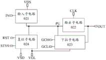
本公开实施例提供一种显示基板,可以解决过孔易被腐蚀的问题。图1是本公开实施例提供的一种显示基板。如图1所示,该显示基板可以包括:Embodiments of the present disclosure provide a display substrate, which can solve the problem that the via hole is easily corroded. FIG. 1 is a display substrate provided by an embodiment of the present disclosure. As shown in FIG. 1, the display substrate may include:
衬底基板01,该衬底基板01可以具有显示区A1和围绕显示区A1的非显示区A2。其中,该显示区A1中设置有多个阵列排布的像素。该非显示区A2可以包括沿远离显示区A1的方向依次排布的周边区A21和封装区A22,该封装区A22内可以涂覆有封装胶(图1中未示出)。A
栅极驱动电路02,该栅极驱动电路02可以位于非显示区A2。该栅极驱动电路02可以用于为该显示区A1中的一行或多行像素提供栅极驱动信号。The
例如,参考图1,其示出的栅极驱动电路02,部分位于非显示区A2包括的周边区A21,部分位于非显示区A2包括的封装区A22。For example, referring to FIG. 1 , the
多条第一信号线03,该多条第一信号线03可以位于周边区A21,且该多条第一信号线03可以与栅极驱动电路02连接。A plurality of
多条第二信号线04,该多条第二信号线04可以位于非显示区A2,且该多条第二信号线04可以与栅极驱动电路02连接。A plurality of
例如,参考图1,其示出的多条第二信号线04均位于非显示区A2包括的封装区A22。For example, referring to FIG. 1 , the plurality of
其中,该第一信号线03和第二信号线04可以均用于为栅极驱动电路02提供信号,且该第一信号线03提供的信号的频率,可以低于第二信号线04提供的信号的频率。即,第一信号线03可以为低频信号线,第二信号线04可以为高频信号线。低频信号线是指频率范围较低、信号变化缓慢且波形较为平滑的信号线,高频信号线是指频率范围较高、信号变化快速且波形易突变的信号线。Wherein, the
基于上述过孔腐蚀原理分析,由于ITO导电膜层连接低频信号线时易与水汽发生反应,因此本公开实施例通过将低频信号线设置于非封装胶涂覆区域,以避免封装胶封装不良导致水汽进入时造成过孔腐蚀的现象。Based on the analysis of the above-mentioned via corrosion principle, since the ITO conductive film layer is prone to react with water vapor when connecting the low-frequency signal line, the embodiment of the present disclosure disposes the low-frequency signal line in the non-encapsulation adhesive coating area to avoid poor encapsulation by the encapsulant. The phenomenon of via corrosion caused by the entry of water vapor.
综上所述,本公开实施例提供了一种显示基板,该显示基板包括具有显示区和非显示区的衬底基板,栅极驱动电路,以及与栅极驱动电路连接的第一信号线和第二信号线,该非显示区包括涂覆封装胶的封装区和周边区。由于用于提供较低频率的信号的第一信号线位于周边区而不位于封装区,因此第一信号线不会被封装胶所覆盖。由此,可以避免因封装不良导致水汽进入封装区域,造成过孔受低频信号线影响而被腐蚀的问题。本公开实施例提供的显示基板的良率较高,显示效果较好。To sum up, the embodiments of the present disclosure provide a display substrate, the display substrate includes a base substrate having a display area and a non-display area, a gate driving circuit, and a first signal line connected to the gate driving circuit and For the second signal line, the non-display area includes an encapsulation area coated with encapsulant and a peripheral area. Since the first signal line for providing the lower frequency signal is located in the peripheral area and not located in the packaging area, the first signal line will not be covered by the encapsulant. In this way, the problem of water vapor entering the packaging area due to poor packaging can be avoided, causing the via hole to be corroded due to the influence of the low-frequency signal line. The display substrate provided by the embodiment of the present disclosure has higher yield and better display effect.
可选的,为了驱动栅极驱动电路02正常工作,栅极驱动电路02一般需要与用于提供直流电源信号的直流电源线,用于提供时钟信号的时钟信号线,和/或用于提供起始驱动信号的起始信号线连接。Optionally, in order to drive the
而由于时钟信号线提供的时钟信号的波形变化较频繁,直流电源线不存在波形变化,起始信号线一般仅波形变化一次。因此可知,时钟信号线相对于直流电源线和起始信号线属于高频信号线,即,直流电源线和起始信号线可以划分为低频信号线。因此,在本公开实施例中,该第一信号线03可以包括直流电源线,和/或,起始信号线。该第二信号线04可以包括:时钟信号线。However, since the waveform of the clock signal provided by the clock signal line changes frequently, there is no waveform change in the DC power line, and the starting signal line generally only changes the waveform once. Therefore, it can be known that the clock signal line is a high frequency signal line relative to the DC power supply line and the start signal line, that is, the DC power supply line and the start signal line can be divided into low frequency signal lines. Therefore, in this embodiment of the present disclosure, the
可选的,图2是本公开实施例提供的一种栅极驱动电路的结构示意图。如图2所示,该栅极驱动电路02可以包括:输入子电路021、输出子电路022、下拉子电路023和复位子电路024。Optionally, FIG. 2 is a schematic structural diagram of a gate driving circuit provided by an embodiment of the present disclosure. As shown in FIG. 2 , the
其中,输入子电路021可以分别与输入信号端IN、第一电源线VDS和上拉节点PU连接。该输入子电路021可以用于响应于输入信号端IN提供的输入信号,向上拉节点PU输出第一电源线VDS提供的第一电源信号。The
可选的,该第一电源信号可以为直流电源信号,且该第一电源信号的电位可以为有效电位。或者,该第一电源信号可以为非直流电源信号,且仅在输入信号的电位为有效电位时,该第一电源信号的电位为有效电位。Optionally, the first power supply signal may be a DC power supply signal, and the potential of the first power supply signal may be an effective potential. Alternatively, the first power supply signal may be a non-DC power supply signal, and the potential of the first power supply signal is an effective potential only when the potential of the input signal is an effective potential.
示例的,该输入子电路021可以在输入信号端IN提供的输入信号的电位为有效电位时,向上拉节点PU输出处于有效电位的第一电源信号,从而实现对上拉节点PU的充电。Exemplarily, the
该输出子电路022可以分别与上拉节点PU、时钟信号线CLK和输出端OUT连接。该输出子电路022可以用于响应于上拉节点PU的电位,向输出端OUT输出时钟信号线CLK提供的时钟信号。The
示例的,该输出子电路022可以在上拉节点PU的电位为有效电位时,向输出端输出时钟信号线CLK提供的时钟信号。For example, the
该下拉子电路023可以分别与第二电源线GCH、第三电源线GCL、第四电源线VGL、上拉节点PU和输出端OUT连接。该下拉子电路023可以用于响应于上拉节点PU的电位、第二电源线GCH提供的第二电源信号和第三电源线GCL提供的第三电源信号,向上拉节点PU和输出端OUT分别输出第四电源线VGL提供的第四电源信号。The pull-
可选的,该第二电源信号和第三电源信号可以均为直流电源信号。或者,该第二电源信号和第三电源信号可以为非直流电源信号,且在需要对上拉节点PU和输出端OUT降噪时,电位保持为有效电位。该第四电源信号可以为直流电源信号,且该第四电源信号的电位可以为无效电位。Optionally, the second power supply signal and the third power supply signal may both be DC power supply signals. Alternatively, the second power supply signal and the third power supply signal may be non-DC power supply signals, and when it is necessary to reduce noise on the pull-up node PU and the output terminal OUT, the potentials are kept as effective potentials. The fourth power signal may be a DC power signal, and the potential of the fourth power signal may be an inactive potential.
示例的,该下拉子电路023可以在上拉节点PU的电位为无效电位时,在第二电源信号或第三电源信号的控制下,向上拉节点PU和输出端OUT分别输出处于无效电位的第四电源信号,从而实现对上拉节点PU和输出端OUT的降噪。Illustratively, when the potential of the pull-up node PU is an inactive potential, under the control of the second power supply signal or the third power supply signal, the pull-up node PU and the output terminal OUT can respectively output the first power at the inactive potential. Four power supply signals, thereby realizing noise reduction of the pull-up node PU and the output terminal OUT.
该复位子电路024可以分别与复位信号端RST、起始信号线STV0、第五电源线VSD、第四电源线VGL和上拉节点PU连接。该复位子电路024可以用于响应于复位信号端RST提供的复位信号,向上拉节点PU输出第五电源线VSD提供的第五电源信号。以及可以用于响应于起始信号线STV0提供的起始驱动信号,向上拉节点PU输出第四电源信号。The reset sub-circuit 024 may be connected to the reset signal terminal RST, the start signal line STV0, the fifth power line VSD, the fourth power line VGL and the pull-up node PU, respectively. The
可选的,该第五电源信号可以为直流电源信号,且该第五电源信号的电位可以为无效电位。或者,该第五电源信号可以为非直流电源信号,且仅在复位信号的电位为有效电位时,该第五电源信号的电位为有效电位。Optionally, the fifth power supply signal may be a DC power supply signal, and the potential of the fifth power supply signal may be an inactive potential. Alternatively, the fifth power supply signal may be a non-DC power supply signal, and the potential of the fifth power supply signal is an effective potential only when the potential of the reset signal is an effective potential.
示例的,该复位子电路024可以在复位信号端RST提供的复位信号的电位为有效电位时,向上拉节点PU输出处于无效电位的第四电源信号,从而实现对上拉节点PU的降噪。以及,该复位子电路024可以在起始信号线STV0提供的起始驱动信号的电位为有效电位时,向上拉节点PU输出处于无效电位的第四电源信号,从而实现对上拉节点PU的降噪。Exemplarily, the
需要说明的是,该其实信号线STV0可以在每帧扫描开始之前,先提供处于有效电位的起始驱动信号,以实现对上拉节点PU的总复位(total reset),也可以一定程度上改善横纹不良现象。It should be noted that the actual signal line STV0 can provide a start driving signal at an effective potential before the scanning of each frame, so as to realize the total reset of the pull-up node PU, which can also improve to a certain extent. Bad streaks.
可选的,对于图2所示的栅极驱动电路,该栅极驱动电路02可以为11T1C结构,即该栅极驱动电路02可以包括11个薄膜晶体管和1个电容器。当然,该栅极驱动电路02也可以为其他结构,如16T1C。以11T1C结构为例,图3示出了一种栅极驱动电路的结构示意图。Optionally, for the gate driving circuit shown in FIG. 2 , the
参考图3,输入子电路021可以包括第一晶体管M1。该第一晶体管M1的栅极可以与输入信号端IN连接,第一极可以与第一电源线VDS连接,第二极可以与上拉节点PU连接。Referring to FIG. 3, the
继续参考图3,输出子电路022可以包括第二晶体管M2和一个电容器C1。其中,该第二晶体管M2的栅极可以与上拉节点PU连接,第一极可以与时钟信号线CLK连接,第二极可以与输出端OUT连接。该电容器C1的一端可以与上拉节点PU连接,另一端可以与输出端OUT连接。With continued reference to FIG. 3, the
继续参考图3,下拉子电路023可以包括:第三晶体管M3、第四晶体管M4、第五晶体管M5、第六晶体管M6、第七晶体管M7、第八晶体管M8和第九晶体管M9。其中,第三晶体管M3的栅极和第一极可以均与第二电源线GCH连接,第二极可以与第四晶体管M4的栅极和第五晶体管M5的第二极连接。第四晶体管M4的第一极可以与第二电源线GCH连接,第二极可以与下拉节点PD连接。第五晶体管M5的栅极和第六晶体管M6的栅极可以均与上拉节点PU连接,第五晶体管M5的第一极和第六晶体管M6的第一极可以均与第四电源线VGL连接。第六晶体管M6的第二极可以与下拉节点PD连接。第七晶体管M7的栅极和第八晶体管M8的栅极可以均与下拉节点PD连接,第七晶体管M7的第一极和第八晶体管M8的第一极可以与第四电源线VGL连接,第七晶体管M7的第二极可以与上拉节点PU连接,第八晶体管M8的第二极可以与输出端OUT连接。第九晶体管M9的栅极可以与第三电源线GCL连接,第一极可以与第四电源线VGL连接,第二极可以与输出端OUT连接。Continuing to refer to FIG. 3 , the pull-
继续参考图3,复位子电路024可以包括:第十晶体管M10和第十一晶体管M11。其中,该第十晶体管M10的栅极可以与复位信号端RST连接,第一极可以与第五电源线VSD连接,第二极可以与上拉节点PU连接。该第十一晶体管M11的栅极可以与起始信号线STV0连接,第一极可以与第四电源线VGL连接,第二极可以与上拉节点PU连接。Continuing to refer to FIG. 3 , the
还需要说明的是,本公开实施例保护的显示基板可以包括:依次级联的多个栅极驱动电路02。每一级移位寄存器单元的输出端OUT可以分别与上一级移位寄存器单元的输入信号端IN,以及下一级移位寄存器单元的复位信号端RST连接。且,该级联的多个栅极驱动电路02可以采用4相时钟,即可以将该级联的多个栅极驱动电路02划分为多组,每组可以包括四个栅极驱动电路02,且该四个栅极驱动电路02可以依次分别与4条时钟信号线连接。当然,也可以采用6相时钟或8相时钟等其他时钟数量另,可以采用三条起始信号线,与4相时钟同理,可以将级联的多个栅极驱动电路02划分为多组,每组可以包括三个栅极驱动电路02,且该三个栅极驱动电路02可以依次分别与该三条起始信号线连接。当然,也可以采用更多条起始信号线。本公开实施例对此均不作限定。It should also be noted that the display substrate protected by the embodiment of the present disclosure may include: a plurality of
对于图2和图3所示的栅极驱动电路,位于周边区A21的第一信号线03可以包括:第一电源线VDS、第二电源线GCH、第三电源线GCL、第四电源线VGL和第五电源线VSD中的一个或多个。For the gate driving circuit shown in FIG. 2 and FIG. 3 , the
示例的,以图3所示的栅极驱动电路,采用4相时钟,且包括3条起始信号线为例。图4示出了本公开实施例提供的另一种显示基板的结构示意图。参考图4可以看出,其示出的显示基板中,位于周边区A21的第一信号线03包括:第一电源线VDS、第二电源线GCH、第三电源线GCL、第四电源线VGL、第五电源线VSD和起始信号线STV0。位于封装区A22的第二信号线04包括:时钟信号线CLK1、时钟信号线CLK2、时钟信号线CLK3、时钟信号线CLK4和其他两条起始信号线STV1和STV2。As an example, take the gate driving circuit shown in FIG. 3 as an example, which adopts a 4-phase clock and includes 3 start signal lines. FIG. 4 shows a schematic structural diagram of another display substrate provided by an embodiment of the present disclosure. Referring to FIG. 4 , in the display substrate shown, the
通过将较多条低频信号线均设置于周边区A21,可以使得较多过孔也相应的位于周边区A21,不被封装胶所覆盖,进一步避免了过孔被腐蚀的现象。By arranging more low-frequency signal lines in the peripheral area A21, more via holes can be correspondingly located in the peripheral area A21 and not covered by the encapsulant, thereby further avoiding the phenomenon of via holes being corroded.
可选的,该显示基板还可以包括:位于衬底基板01上的晶体管器件层。该晶体管器件层可以用于形成栅极驱动电路02包括的多个薄膜晶体管,如用于形成图3和图4所示的11个薄膜晶体管M1。Optionally, the display substrate may further include: a transistor device layer on the
图5是本公开实施例提供的一种晶体管器件层的结构示意图。如图5所示,该晶体管器件层05可以包括:位于衬底基板01的一侧,且沿远离衬底基板01的方向依次层叠的栅极(gate)层051、栅绝缘(gate insulation,GI)层052、源漏极(source drain,SD)层053、钝化(passivation,PVX)层054和导电膜层ITO 055。需要说明的是,该晶体管器件层可以称为底栅结构。FIG. 5 is a schematic structural diagram of a transistor device layer provided by an embodiment of the present disclosure. As shown in FIG. 5 , the
其中,该晶体管器件层05中可以设置有过孔K,该过孔K可以用于连接晶体管器件层05中的栅极层051和源漏极层053,使得栅极层051和源漏极层053之间的信号导通。即,每个过孔K均可以与栅极层051和源漏极层053同层设置,且每个过孔K需要贯穿至栅极层051,使得栅极层051暴露出来,以便导电膜层055设置于该过孔K内时,能够电连接栅极层051和源漏极层053。The
可选的,在本公开实施例中,因第一信号线03的位置设置,可以使得每个栅极驱动电路02所在区域中设置的过孔的数量,小于栅极驱动电路02包括的薄膜晶体管M1的数量。由于降低了过孔的设置数量,因此还避免了因较多数量的过孔被腐蚀而更易造成横纹不良现象。Optionally, in the embodiment of the present disclosure, due to the location of the
例如,参考图4,其示出的每个栅极驱动电路02共包括11个薄膜晶体管M1。每个栅极驱动电路02所在区域中共设置有十个过孔K1至K10。该十个过孔K1至K10中,每个过孔的结构均可以参考图5示出的过孔K的结构。For example, referring to FIG. 4 , each
可选的,以图4所示的显示基板为例,图6示出了一种仅包括衬底基板01和过孔的结构示意图。如图6所示,该十个过孔中,仅一个过孔K1可以位于封装区A22,其余过孔(如,图4所示的过孔K2至K10)可以均位于周边区A21。Optionally, taking the display substrate shown in FIG. 4 as an example, FIG. 6 shows a schematic structural diagram that only includes a
例如,结合图4示出的栅极驱动电路可知,该位于封装区A22的一个过孔K1可以为用于将时钟信号线CLK1接入薄膜晶体管M2的第一极的过孔,使得当薄膜晶体管M2在栅极电位的控制下导通时,时钟信号线CLK1可以将时钟信号输出至薄膜晶体管M2的第二极。位于周边区A21的其余过孔K2至K10中:For example, with reference to the gate driving circuit shown in FIG. 4 , the via hole K1 in the packaging area A22 may be a via hole for connecting the clock signal line CLK1 to the first pole of the thin film transistor M2, so that when the thin film transistor M2 When M2 is turned on under the control of the gate potential, the clock signal line CLK1 can output the clock signal to the second pole of the thin film transistor M2. In the remaining vias K2 to K10 in the peripheral area A21:
过孔K2,可以用于将第四电源线VGL接入薄膜晶体管M9的第一极,使得当薄膜晶体管M9在栅极电位的控制下导通时,第四电源线VGL可以将第四电源信号输出至薄膜晶体管M9的第二极。The via hole K2 can be used to connect the fourth power supply line VGL to the first pole of the thin film transistor M9, so that when the thin film transistor M9 is turned on under the control of the gate potential, the fourth power supply line VGL can connect the fourth power supply signal output to the second pole of the thin film transistor M9.
过孔K3,可以用于将薄膜晶体管M2的第二极和薄膜晶体管M9的第二极接入输出端OUT,进而使得薄膜晶体管M2向输出端OUT输出时钟信号,或,使得薄膜晶体管M9向输出端OUT输出第四电源信号。The via hole K3 can be used to connect the second pole of the thin film transistor M2 and the second pole of the thin film transistor M9 to the output terminal OUT, thereby enabling the thin film transistor M2 to output a clock signal to the output terminal OUT, or to enable the thin film transistor M9 to output a clock signal to the output terminal OUT. The terminal OUT outputs a fourth power supply signal.
过孔K4,可以用于将第五电源线VSD接入薄膜晶体管M10的第一极,使得当薄膜晶体管M10在栅极电位的控制下导通时,第五电源线VSD可以将第五电源信号输出至薄膜晶体管M10的第二极。The via hole K4 can be used to connect the fifth power supply line VSD to the first pole of the thin film transistor M10, so that when the thin film transistor M10 is turned on under the control of the gate potential, the fifth power supply line VSD can connect the fifth power supply signal output to the second pole of the thin film transistor M10.
过孔K5,可以用于将第一电源线VDS接入薄膜晶体管M1的第一极,使得当薄膜晶体管M1在栅极电位的控制下导通时,第一电源线VDS可以将第一电源信号输出至薄膜晶体管M1的第二极。The via hole K5 can be used to connect the first power supply line VDS to the first pole of the thin film transistor M1, so that when the thin film transistor M1 is turned on under the control of the gate potential, the first power supply line VDS can connect the first power supply signal output to the second pole of the thin film transistor M1.
过孔K6,可以用于将第四电源线VGL接入薄膜晶体管M11的第一极,使得当薄膜晶体管M11在栅极电位的控制下导通时,第四电源线VGL可以将第四电源信号输出至薄膜晶体管M11的第二极。The via hole K6 can be used to connect the fourth power supply line VGL to the first pole of the thin film transistor M11, so that when the thin film transistor M11 is turned on under the control of the gate potential, the fourth power supply line VGL can connect the fourth power supply signal output to the second pole of the thin film transistor M11.
过孔K7,可以用于将第第二电源线GCH接入薄膜晶体管M4的第一极,使得当薄膜晶体管M4在栅极电位的控制下导通时,第二电源线GCH可以将第一电源信号输出至薄膜晶体管M4的第二极。The via hole K7 can be used to connect the second power line GCH to the first pole of the thin film transistor M4, so that when the thin film transistor M4 is turned on under the control of the gate potential, the second power line GCH can connect the first power The signal is output to the second pole of the thin film transistor M4.
过孔K8,可以用于将薄膜晶体管M3的第二极与薄膜晶体管M4的栅极电连接,使得薄膜晶体管M3第二极的电位可以输出至薄膜晶体管M4的栅极,以控制薄膜晶体管M4的通断状态。The via hole K8 can be used to electrically connect the second pole of the thin film transistor M3 to the gate of the thin film transistor M4, so that the potential of the second pole of the thin film transistor M3 can be output to the gate of the thin film transistor M4 to control the gate of the thin film transistor M4. On-off state.
过孔K9,可以用于将薄膜晶体管M4的第二极和薄膜晶体管M8的栅极电连接,使得薄膜晶体管M4第二极的电位可以输出至薄膜晶体管M8的栅极,以控制薄膜晶体管M8的通断状态。The via hole K9 can be used to electrically connect the second pole of the thin film transistor M4 and the gate of the thin film transistor M8, so that the potential of the second pole of the thin film transistor M4 can be output to the gate of the thin film transistor M8, so as to control the gate of the thin film transistor M8. On-off state.
过孔K10,可以作为上拉节点PU与各薄膜晶体管(如,M2、M6、M7、M11、M1和M10)连通的一个过孔,以实现对各薄膜晶体管的控制,或,控制各薄膜晶体管的通断状态。The via hole K10 can be used as a via hole connecting the pull-up node PU with each thin film transistor (eg, M2, M6, M7, M11, M1, and M10) to realize the control of each thin film transistor, or to control each thin film transistor on-off state.
需要说明的是,上述第一极可以为薄膜晶体管的源极,相应的,第二极可以为薄膜晶体管的漏极;或者,上述第一极可以为薄膜晶体管的漏极,相应的,第二极可以为薄膜晶体管的源极。It should be noted that the first electrode may be the source electrode of the thin film transistor, and correspondingly, the second electrode may be the drain electrode of the thin film transistor; or, the first electrode may be the drain electrode of the thin film transistor, correspondingly, the second electrode The electrode may be the source electrode of the thin film transistor.
另,结合图4和图6所示大小的显示基板,位于封装区A22的一个过孔K1,距封装区A22靠近周边区A21的距离可以为450微米(μm)。当然,对于不同面积的显示基板,该位于封装区A22的一个过孔K1,距封装区A22靠近周边区A21的距离可以不同。图6示出的A22中填充的图案可以为封装胶。L1为切割线,即,L1所在位置即为显示基板(panel)的边缘。通过在封装区设置数量较少的过孔,可以避免较多过孔被腐蚀而带来更为严重的横纹不良现象。4 and 6, a via hole K1 in the packaging area A22 may be 450 micrometers (μm) away from the packaging area A22 and the peripheral area A21. Of course, for display substrates with different areas, the distance from the via hole K1 in the packaging area A22 to the packaging area A22 and the peripheral area A21 may be different. The pattern filled in A22 shown in FIG. 6 may be encapsulant. L1 is the cutting line, that is, the position of L1 is the edge of the display panel. By arranging a smaller number of via holes in the package area, it is possible to prevent more via holes from being corroded and cause more serious horizontal streak defects.
对于图3所示结构的栅极驱动电路,相关技术中,由于起始信号线STV0、第二电源线GCH和第四电源线VGL均设置于封装区A22,因此为了保证各薄膜晶体管与各信号线的可靠连接,过孔的数量需要大于栅极驱动电路包括的薄膜晶体管的数量。如,过孔的数量一般约为12个。且,较多数量的过孔一般会位于封装区A22。如,封装区A22包括的过孔数量一般约为5个。除此之外,封装区A22内,距封装区A22靠近周边区A21最近的过孔,距封装区A22靠近周边区A21一侧的距离也会较短,一般大约为240μm。另,栅极驱动电路02所占区域宽度也会较大,一般约为660μm。For the gate driving circuit with the structure shown in FIG. 3, in the related art, since the start signal line STV0, the second power line GCH and the fourth power line VGL are all arranged in the packaging area A22, in order to ensure that each thin film transistor and each signal For reliable connection of lines, the number of vias needs to be greater than the number of thin film transistors included in the gate driving circuit. For example, the number of vias is generally about 12. Also, a larger number of vias are generally located in the package area A22. For example, the number of vias included in the package area A22 is generally about five. In addition, in the packaging area A22, the distance from the via hole closest to the packaging area A22 to the peripheral area A21 is also shorter, generally about 240 μm. In addition, the width of the area occupied by the
而本公开实施例通过将第一信号线03设置于栅极驱动电路02靠近显示区A1的一侧,即设置于栅极驱动电路02的内侧,不仅可以使得原来的过孔由12个减少至10个,且可以将封装区A22内的过孔数量由5个减少至1个,且可以使得位于封装区A22的1个过孔距封装区A22靠近周边区A21一侧的距离增加至450μm。除此之外,本公开实施例的设置方式还可以使得栅极驱动电路02所占区域宽度由相关技术中的660μm减少至640μm。通过该设置方式,在实现窄边框的前提下,有效可靠的避免了封装胶封装不良导致的过孔腐蚀现象。另,为进一步确保过孔不被腐蚀,还可以使用防水性能较好的封装胶进行封装。In the embodiment of the present disclosure, by arranging the
可选的,结合上述图1和图4,本公开实施例记载的多条第二信号线04可以均位于封装区A22。当然,为进一步确保良率,该多条第二信号线04还可以位于周边区A21。即,所有与栅极驱动电路02连接的信号线均不被封装胶覆盖。Optionally, with reference to the foregoing FIG. 1 and FIG. 4 , the plurality of
图7以非显示区A2包括十二条信号线,且其中六条信号线位于周边区,六条信号线位于封装区为例,示出了又一种显示基板的结构示意图。如图7可以看出,封装胶S1在封装区域的涂覆宽度可以为650μm,且涂覆后,封装胶S1分别向左右两侧溢出100μm。切割线L1一般位于封装胶S1靠近周边区100μm的位置处。即切割线L1距封装区靠近显示区一侧的距离为550μm。另,切割线L1距非显示区A2靠近显示区A1一侧的距离可以为1000μm。FIG. 7 is an example of a non-display area A2 including twelve signal lines, six signal lines located in the peripheral area and six signal lines located in the packaging area, showing a schematic structural diagram of another display substrate. As can be seen from FIG. 7 , the coating width of the encapsulant S1 in the encapsulation area can be 650 μm, and after coating, the encapsulant S1 overflows 100 μm to the left and right sides respectively. The cutting line L1 is generally located at a position of 100 μm near the peripheral area of the encapsulant S1 . That is, the distance between the cutting line L1 and the side of the packaging area close to the display area is 550 μm. In addition, the distance between the cutting line L1 and the side of the non-display area A2 close to the display area A1 may be 1000 μm.
需要说明的是,图7仅是一种示意性说明,基于不同面积的显示基板,封装胶的涂覆宽度可以不同。另,非显示区A2的面积一般远小于显示区A1的面积,本公开实施例附图示出的显示区A1和非显示区A2的比例仅是示意性说明,综上所述,本公开实施例提供了一种显示基板,该显示基板包括具有显示区和非显示区的衬底基板,栅极驱动电路,以及与栅极驱动电路连接的第一信号线和第二信号线,该非显示区包括涂覆封装胶的封装区和周边区。由于用于提供较低频率的信号的第一信号线位于周边区而不位于封装区,因此第一信号线不会被封装胶所覆盖。由此,可以避免因封装不良导致水汽进入封装区域,造成过孔受低频信号线影响而被腐蚀的问题。本公开实施例提供的显示基板的良率较高,显示效果较好。It should be noted that FIG. 7 is only a schematic illustration, and based on the display substrates of different areas, the coating width of the encapsulant may be different. In addition, the area of the non-display area A2 is generally much smaller than the area of the display area A1. The ratio of the display area A1 and the non-display area A2 shown in the drawings in the embodiments of the present disclosure is only a schematic illustration. An example provides a display substrate, the display substrate includes a base substrate having a display area and a non-display area, a gate driving circuit, and a first signal line and a second signal line connected to the gate driving circuit, the non-display area The zone includes the encapsulation zone and the peripheral zone where the encapsulant is applied. Since the first signal line for providing the lower frequency signal is located in the peripheral area and not located in the packaging area, the first signal line will not be covered by the encapsulant. In this way, the problem of water vapor entering the packaging area due to poor packaging can be avoided, causing the via hole to be corroded due to the influence of the low-frequency signal line. The display substrate provided by the embodiment of the present disclosure has higher yield and better display effect.
图8是本公开实施例提供的一种显示基板的制造方法,可以用于制造如图1或图4所示的显示基板。如图8所示,该方法可以包括:FIG. 8 is a method for manufacturing a display substrate provided by an embodiment of the present disclosure, which can be used to manufacture the display substrate as shown in FIG. 1 or FIG. 4 . As shown in Figure 8, the method may include:
步骤801、提供衬底基板。
可选的,参考图1,该衬底基板可以具有显示区A1和围绕显示区A1的非显示区A2。该非显示区A2可以包括沿远离显示区A1的方向依次排布的周边区A21和封装区A22。且,该封装区A22内可以涂覆有封装胶。Optionally, referring to FIG. 1 , the base substrate may have a display area A1 and a non-display area A2 surrounding the display area A1. The non-display area A2 may include a peripheral area A21 and an encapsulation area A22 sequentially arranged in a direction away from the display area A1. Furthermore, the encapsulation area A22 may be coated with an encapsulant.
步骤802、在非显示区,形成栅极驱动电路。
可选的,参考图1和图4,可以在部分周边区A21和部分封装区A22形式栅极驱动电路02。Optionally, referring to FIG. 1 and FIG. 4 , the
步骤803、在周边区,形成与栅极驱动电路连接的多条第一信号线。
可选的,参考图1,可以仅在未涂覆有封装胶的周边区A21形成与栅极驱动电路02连接的多条第一信号线03。Optionally, referring to FIG. 1 , a plurality of
步骤804、在非显示区,形成与栅极驱动电路连接的多条第二信号线。
可选的,参考图1,可以仅在涂覆有封装胶的封装区A22形成与栅极驱动电路02连接的多条第二信号线04。或者,可以仅在周边区A21形成与栅极驱动电路02连接的多条第二信号线04。又或者,可以在部分周边区A21和部分封装区A22形成与栅极驱动电路02连接的多条第二信号线04。Optionally, referring to FIG. 1 , a plurality of
其中,该第一信号线03和第二信号线04可以均用于为栅极驱动电路02提供信号,且该第一信号线03提供的信号的频率,可以低于第二信号线04提供的信号的频率。即,该第一信号线03可以为低频信号线,第二信号线04可以为高频信号线。Wherein, the
综上所述,本公开实施例提供了一种显示基板的制造方法。该方法包括:形成具有显示区和非显示区的衬底基板,栅极驱动电路,以及与栅极驱动电路连接的第一信号线和第二信号线,该非显示区包括涂覆封装胶的封装区和周边区。由于是在周边区而不是封装区形成提供较低频率的信号的第一信号线,因此可以使得第一信号线不会被封装胶所覆盖。由此,可以避免因封装不良导致水汽进入封装区域,造成过孔受低频信号线影响而被腐蚀的问题。本公开实施例提供的显示基板的制造方法制成的显示基板的良率较高,显示效果较好。To sum up, the embodiments of the present disclosure provide a method for manufacturing a display substrate. The method includes: forming a base substrate having a display area and a non-display area, a gate driving circuit, and a first signal line and a second signal line connected to the gate driving circuit, the non-display area comprising a sealing compound coated with an encapsulant. package area and surrounding area. Since the first signal line for providing a lower frequency signal is formed in the peripheral area instead of the package area, the first signal line can be prevented from being covered by the encapsulation glue. In this way, the problem of water vapor entering the packaging area due to poor packaging can be avoided, causing the via hole to be corroded due to the influence of the low-frequency signal line. The display substrate produced by the manufacturing method of the display substrate provided by the embodiment of the present disclosure has a higher yield and better display effect.
图9是本公开实施例提供的一种显示装置的结构示意图。如图9所示,该显示装置可以包括:信号提供电路10,以及如图1或图4所示的显示基板20。该信号提供电路10可以与显示基板20包括的信号线连接,该信号提供电路10可以用于向信号线提供驱动信号。如,该信号提供电路10可以为时序控制器。FIG. 9 is a schematic structural diagram of a display device provided by an embodiment of the present disclosure. As shown in FIG. 9 , the display device may include: a
例如,结合图1和图9,该显示基板20可以包括多条第一信号线03和多条第二信号线04,该信号提供电路10可以与每条第一信号线03和每条第二信号线04连接,并用于为该每条第一信号线03和每条第二信号线04提供驱动信号。For example, referring to FIG. 1 and FIG. 9 , the
可选的,该显示装置可以为:液晶显示器、电子纸、手机、平板电脑、电视机、显示器、笔记本电脑等任何具有显示功能的产品或部件。Optionally, the display device may be any product or component with display function, such as liquid crystal display, electronic paper, mobile phone, tablet computer, television, monitor, notebook computer, etc.
需要指出的是,在附图中,为了图示的清晰可能夸大了层和区域的尺寸。而且可以理解,当元件或层被称为在另一元件或层“上”时,它可以直接在其他元件上,或者可以存在中间的层。另外,可以理解,当元件或层被称为在另一元件或层“下”时,它可以直接在其他元件下,或者可以存在一个以上的中间的层或元件。另外,还可以理解,当层或元件被称为在两层或两个元件“之间”时,它可以为两层或两个元件之间惟一的层,或还可以存在一个以上的中间层或元件。通篇相似的参考标记指示相似的元件。It should be noted that, in the drawings, the sizes of layers and regions may be exaggerated for clarity of illustration. It will also be understood that when an element or layer is referred to as being "on" another element or layer, it can be directly on the other element or intervening layers may be present. In addition, it will be understood that when an element or layer is referred to as being "under" another element or layer, it can be directly under the other element, or more than one intervening layer or element may be present. In addition, it will also be understood that when a layer or element is referred to as being 'between' two layers or elements, it can be the only layer between the two layers or elements, or more than one intervening layer may also be present or element. Like reference numerals indicate like elements throughout.
术语“第一”和“第二”仅用于描述目的,而不能理解为指示或暗示相对重要性。术语“多个”指两个或两个以上,除非另有明确的限定。术语“和/或”,仅是一种描述关联对象的关联关系,表示可以存在三种关系,例如,A和/或B,可以表示:单独存在A,同时存在A和B,单独存在B这三种情况。The terms "first" and "second" are used for descriptive purposes only and should not be construed to indicate or imply relative importance. The term "plurality" refers to two or more, unless expressly limited otherwise. The term "and/or" is only an association relationship to describe associated objects, which means that there can be three kinds of relationships, for example, A and/or B, which can mean that A exists alone, A and B exist at the same time, and B exists alone. three conditions.
以上所述仅为本公开的可选实施例,并不用以限制本公开实施例,凡在本公开实施例的精神和原则之内,所作的任何修改、等同替换、改进等,均应包含在本公开实施例的保护范围之内。The above descriptions are only optional embodiments of the present disclosure, and are not intended to limit the embodiments of the present disclosure. Any modifications, equivalent replacements, improvements, etc. made within the spirit and principles of the embodiments of the present disclosure shall be included in the within the protection scope of the embodiments of the present disclosure.
Claims (15)
Translated fromChinesePriority Applications (3)
| Application Number | Priority Date | Filing Date | Title |
|---|---|---|---|
| CN202010327231.9ACN111487825B (en) | 2020-04-23 | 2020-04-23 | Display substrate, manufacturing method thereof, and display device |
| PCT/CN2021/079709WO2021213036A1 (en) | 2020-04-23 | 2021-03-09 | Display substrate and method for manufacturing same, and display apparatus |
| US17/764,448US11927844B2 (en) | 2020-04-23 | 2021-03-09 | Display substrate and method for manufacturing same, and display device |
Applications Claiming Priority (1)
| Application Number | Priority Date | Filing Date | Title |
|---|---|---|---|
| CN202010327231.9ACN111487825B (en) | 2020-04-23 | 2020-04-23 | Display substrate, manufacturing method thereof, and display device |
Publications (2)
| Publication Number | Publication Date |
|---|---|
| CN111487825Atrue CN111487825A (en) | 2020-08-04 |
| CN111487825B CN111487825B (en) | 2023-05-12 |
Family
ID=71794815
Family Applications (1)
| Application Number | Title | Priority Date | Filing Date |
|---|---|---|---|
| CN202010327231.9AActiveCN111487825B (en) | 2020-04-23 | 2020-04-23 | Display substrate, manufacturing method thereof, and display device |
Country Status (3)
| Country | Link |
|---|---|
| US (1) | US11927844B2 (en) |
| CN (1) | CN111487825B (en) |
| WO (1) | WO2021213036A1 (en) |
Cited By (7)
| Publication number | Priority date | Publication date | Assignee | Title |
|---|---|---|---|---|
| CN113219740A (en)* | 2021-04-20 | 2021-08-06 | 绵阳惠科光电科技有限公司 | Display panel and display device |
| WO2021213036A1 (en)* | 2020-04-23 | 2021-10-28 | 京东方科技集团股份有限公司 | Display substrate and method for manufacturing same, and display apparatus |
| CN115273726A (en)* | 2022-09-01 | 2022-11-01 | 合肥鑫晟光电科技有限公司 | Display substrate, display panel and display device |
| WO2022252092A1 (en)* | 2021-05-31 | 2022-12-08 | 京东方科技集团股份有限公司 | Shift register unit and drive method therefor, gate driver circuit, and display device |
| CN119126440A (en)* | 2024-08-30 | 2024-12-13 | 绵阳惠科光电科技有限公司 | Display panel and display device |
| WO2025086913A1 (en)* | 2023-10-26 | 2025-05-01 | 京东方科技集团股份有限公司 | Array substrate and display device |
| CN119126440B (en)* | 2024-08-30 | 2025-10-10 | 绵阳惠科光电科技有限公司 | Display panel and display device |
Families Citing this family (1)
| Publication number | Priority date | Publication date | Assignee | Title |
|---|---|---|---|---|
| WO2023159592A1 (en)* | 2022-02-28 | 2023-08-31 | 京东方科技集团股份有限公司 | Circuit board, display substrate and display apparatus |
Citations (12)
| Publication number | Priority date | Publication date | Assignee | Title |
|---|---|---|---|---|
| CN1549997A (en)* | 2002-04-08 | 2004-11-24 | ���ǵ�����ʽ���� | Liquid crystal display device with a light guide plate |
| CN1760946A (en)* | 2004-09-13 | 2006-04-19 | 三星电子株式会社 | Driver element and have a display device of this driver element |
| CN101038384A (en)* | 2002-04-08 | 2007-09-19 | 三星电子株式会社 | Liquid crystal display device |
| CN102640042A (en)* | 2009-12-04 | 2012-08-15 | 夏普株式会社 | Liquid crystal display device |
| US20130076716A1 (en)* | 2011-09-22 | 2013-03-28 | Sung-hoon Lim | Liquid crystal display |
| CN105185345A (en)* | 2015-10-23 | 2015-12-23 | 京东方科技集团股份有限公司 | Grid electrode driving circuit, driving method thereof and display panel |
| CN106023945A (en)* | 2016-08-03 | 2016-10-12 | 京东方科技集团股份有限公司 | Grid driving circuit and driving method thereof and display device |
| CN107134264A (en)* | 2016-02-26 | 2017-09-05 | 瀚宇彩晶股份有限公司 | Drive circuit and display device |
| CN108305581A (en)* | 2018-02-12 | 2018-07-20 | 京东方科技集团股份有限公司 | A kind of shift register and gate driving circuit |
| CN108538237A (en)* | 2018-04-26 | 2018-09-14 | 京东方科技集团股份有限公司 | A kind of gate driving circuit, method and display device |
| CN108564912A (en)* | 2018-04-18 | 2018-09-21 | 京东方科技集团股份有限公司 | Shift-register circuit and driving method, display device |
| CN109637447A (en)* | 2019-02-27 | 2019-04-16 | 合肥京东方卓印科技有限公司 | Display base plate and preparation method thereof, display panel |
Family Cites Families (9)
| Publication number | Priority date | Publication date | Assignee | Title |
|---|---|---|---|---|
| CN103293736B (en)* | 2012-09-05 | 2015-12-16 | 上海天马微电子有限公司 | Embedded liquid crystal touch panel |
| KR102052933B1 (en)* | 2012-11-27 | 2019-12-09 | 삼성디스플레이 주식회사 | Display substrate |
| CN106531044B (en) | 2015-09-11 | 2019-09-03 | 南京瀚宇彩欣科技有限责任公司 | Display panel and its gate drive circuit |
| KR102479020B1 (en) | 2017-11-28 | 2022-12-19 | 삼성디스플레이 주식회사 | Display device |
| KR102689438B1 (en)* | 2018-11-06 | 2024-07-26 | 삼성디스플레이 주식회사 | Display device |
| CN110706639A (en)* | 2019-11-15 | 2020-01-17 | 京东方科技集团股份有限公司 | Shift register unit and driving method thereof, gate driving circuit, and display device |
| CN111210755A (en)* | 2020-02-25 | 2020-05-29 | 合肥京东方光电科技有限公司 | Shift register, grid drive circuit and display panel |
| CN111243489B (en)* | 2020-03-24 | 2022-11-01 | 合肥鑫晟光电科技有限公司 | Shifting register, driving method thereof and grid driving circuit |
| CN111487825B (en)* | 2020-04-23 | 2023-05-12 | 京东方科技集团股份有限公司 | Display substrate, manufacturing method thereof, and display device |
- 2020
- 2020-04-23CNCN202010327231.9Apatent/CN111487825B/enactiveActive
- 2021
- 2021-03-09USUS17/764,448patent/US11927844B2/enactiveActive
- 2021-03-09WOPCT/CN2021/079709patent/WO2021213036A1/ennot_activeCeased
Patent Citations (12)
| Publication number | Priority date | Publication date | Assignee | Title |
|---|---|---|---|---|
| CN1549997A (en)* | 2002-04-08 | 2004-11-24 | ���ǵ�����ʽ���� | Liquid crystal display device with a light guide plate |
| CN101038384A (en)* | 2002-04-08 | 2007-09-19 | 三星电子株式会社 | Liquid crystal display device |
| CN1760946A (en)* | 2004-09-13 | 2006-04-19 | 三星电子株式会社 | Driver element and have a display device of this driver element |
| CN102640042A (en)* | 2009-12-04 | 2012-08-15 | 夏普株式会社 | Liquid crystal display device |
| US20130076716A1 (en)* | 2011-09-22 | 2013-03-28 | Sung-hoon Lim | Liquid crystal display |
| CN105185345A (en)* | 2015-10-23 | 2015-12-23 | 京东方科技集团股份有限公司 | Grid electrode driving circuit, driving method thereof and display panel |
| CN107134264A (en)* | 2016-02-26 | 2017-09-05 | 瀚宇彩晶股份有限公司 | Drive circuit and display device |
| CN106023945A (en)* | 2016-08-03 | 2016-10-12 | 京东方科技集团股份有限公司 | Grid driving circuit and driving method thereof and display device |
| CN108305581A (en)* | 2018-02-12 | 2018-07-20 | 京东方科技集团股份有限公司 | A kind of shift register and gate driving circuit |
| CN108564912A (en)* | 2018-04-18 | 2018-09-21 | 京东方科技集团股份有限公司 | Shift-register circuit and driving method, display device |
| CN108538237A (en)* | 2018-04-26 | 2018-09-14 | 京东方科技集团股份有限公司 | A kind of gate driving circuit, method and display device |
| CN109637447A (en)* | 2019-02-27 | 2019-04-16 | 合肥京东方卓印科技有限公司 | Display base plate and preparation method thereof, display panel |
Cited By (12)
| Publication number | Priority date | Publication date | Assignee | Title |
|---|---|---|---|---|
| WO2021213036A1 (en)* | 2020-04-23 | 2021-10-28 | 京东方科技集团股份有限公司 | Display substrate and method for manufacturing same, and display apparatus |
| US11927844B2 (en) | 2020-04-23 | 2024-03-12 | Beijing Boe Optoelectronics Technology Co., Ltd. | Display substrate and method for manufacturing same, and display device |
| CN113219740A (en)* | 2021-04-20 | 2021-08-06 | 绵阳惠科光电科技有限公司 | Display panel and display device |
| CN113219740B (en)* | 2021-04-20 | 2023-08-29 | 绵阳惠科光电科技有限公司 | Display panel and display device |
| WO2022252092A1 (en)* | 2021-05-31 | 2022-12-08 | 京东方科技集团股份有限公司 | Shift register unit and drive method therefor, gate driver circuit, and display device |
| CN115273726A (en)* | 2022-09-01 | 2022-11-01 | 合肥鑫晟光电科技有限公司 | Display substrate, display panel and display device |
| WO2024045988A1 (en)* | 2022-09-01 | 2024-03-07 | 京东方科技集团股份有限公司 | Display substrate, display panel, and display apparatus |
| CN115273726B (en)* | 2022-09-01 | 2025-08-29 | 合肥鑫晟光电科技有限公司 | Display substrate, display panel, and display device |
| US12424184B2 (en) | 2022-09-01 | 2025-09-23 | Hefei Xinsheng Optoelectronics Technology Co., Ltd. | Display baseplate, display panel, and display apparatus |
| WO2025086913A1 (en)* | 2023-10-26 | 2025-05-01 | 京东方科技集团股份有限公司 | Array substrate and display device |
| CN119126440A (en)* | 2024-08-30 | 2024-12-13 | 绵阳惠科光电科技有限公司 | Display panel and display device |
| CN119126440B (en)* | 2024-08-30 | 2025-10-10 | 绵阳惠科光电科技有限公司 | Display panel and display device |
Also Published As
| Publication number | Publication date |
|---|---|
| CN111487825B (en) | 2023-05-12 |
| WO2021213036A1 (en) | 2021-10-28 |
| US11927844B2 (en) | 2024-03-12 |
| US20230030213A1 (en) | 2023-02-02 |
Similar Documents
| Publication | Publication Date | Title |
|---|---|---|
| CN111487825B (en) | Display substrate, manufacturing method thereof, and display device | |
| CN110264891B (en) | Array substrate, display panel and display device | |
| CN108598087A (en) | Array substrate and its manufacturing method, display panel, electronic device | |
| CN204595383U (en) | Array substrate, display panel and display device | |
| CN109192767B (en) | Display panel and display device | |
| US11415843B2 (en) | Display panel and liquid crystal display device | |
| WO2020107819A1 (en) | Display device and manufacturing method therefor | |
| CN103389588A (en) | Display panel and packaging method thereof and liquid crystal display device | |
| CN104617106A (en) | Array substrate and display device | |
| CN112802878B (en) | Display panel and display device | |
| US20210208734A1 (en) | Touch display device | |
| CN111736395A (en) | Display panel and display device | |
| WO2020034293A1 (en) | Display panel and bonding method | |
| WO2020124903A1 (en) | Array substrate and display panel | |
| WO2020177500A1 (en) | Display substrate, manufacturing method thereof, and display panel | |
| CN107026191A (en) | OLED display device and control method thereof | |
| CN109637447B (en) | Display substrate and preparation method thereof, and display panel | |
| CN116643424A (en) | Array substrate, display substrate and display device | |
| JP2010039211A (en) | Display device and method for manufacturing the same | |
| CN102760772A (en) | Transistor structure and driving circuit structure | |
| CN110854137A (en) | Display panel, array substrate and manufacturing method thereof | |
| WO2025156830A1 (en) | Display panel, display panel preparation method, and display device | |
| TW201007253A (en) | Connecting structure between display panel and flexible printed circuit board | |
| CN114664904A (en) | Array substrate and display panel | |
| JP7343396B2 (en) | Array substrates, display panels and display devices |
Legal Events
| Date | Code | Title | Description |
|---|---|---|---|
| PB01 | Publication | ||
| PB01 | Publication | ||
| SE01 | Entry into force of request for substantive examination | ||
| SE01 | Entry into force of request for substantive examination | ||
| GR01 | Patent grant | ||
| GR01 | Patent grant |