CN111480110A - Augmented reality display with liquid crystal variable focusing elements and roll-to-roll method and apparatus for forming such a display - Google Patents
Augmented reality display with liquid crystal variable focusing elements and roll-to-roll method and apparatus for forming such a displayDownload PDFInfo
- Publication number
- CN111480110A CN111480110ACN201880081298.XACN201880081298ACN111480110ACN 111480110 ACN111480110 ACN 111480110ACN 201880081298 ACN201880081298 ACN 201880081298ACN 111480110 ACN111480110 ACN 111480110A
- Authority
- CN
- China
- Prior art keywords
- liquid crystal
- substrate
- lens
- wave plate
- roll
- Prior art date
- Legal status (The legal status is an assumption and is not a legal conclusion. Google has not performed a legal analysis and makes no representation as to the accuracy of the status listed.)
- Granted
Links
Images


Classifications
- G—PHYSICS
- G02—OPTICS
- G02B—OPTICAL ELEMENTS, SYSTEMS OR APPARATUS
- G02B27/00—Optical systems or apparatus not provided for by any of the groups G02B1/00 - G02B26/00, G02B30/00
- G02B27/01—Head-up displays
- G02B27/017—Head mounted
- G02B27/0172—Head mounted characterised by optical features
- G—PHYSICS
- G02—OPTICS
- G02B—OPTICAL ELEMENTS, SYSTEMS OR APPARATUS
- G02B27/00—Optical systems or apparatus not provided for by any of the groups G02B1/00 - G02B26/00, G02B30/00
- G02B27/0081—Optical systems or apparatus not provided for by any of the groups G02B1/00 - G02B26/00, G02B30/00 with means for altering, e.g. enlarging, the entrance or exit pupil
- G—PHYSICS
- G02—OPTICS
- G02B—OPTICAL ELEMENTS, SYSTEMS OR APPARATUS
- G02B6/00—Light guides; Structural details of arrangements comprising light guides and other optical elements, e.g. couplings
- G02B6/0001—Light guides; Structural details of arrangements comprising light guides and other optical elements, e.g. couplings specially adapted for lighting devices or systems
- G02B6/0011—Light guides; Structural details of arrangements comprising light guides and other optical elements, e.g. couplings specially adapted for lighting devices or systems the light guides being planar or of plate-like form
- G02B6/0075—Arrangements of multiple light guides
- G02B6/0076—Stacked arrangements of multiple light guides of the same or different cross-sectional area
- G—PHYSICS
- G02—OPTICS
- G02F—OPTICAL DEVICES OR ARRANGEMENTS FOR THE CONTROL OF LIGHT BY MODIFICATION OF THE OPTICAL PROPERTIES OF THE MEDIA OF THE ELEMENTS INVOLVED THEREIN; NON-LINEAR OPTICS; FREQUENCY-CHANGING OF LIGHT; OPTICAL LOGIC ELEMENTS; OPTICAL ANALOGUE/DIGITAL CONVERTERS
- G02F1/00—Devices or arrangements for the control of the intensity, colour, phase, polarisation or direction of light arriving from an independent light source, e.g. switching, gating or modulating; Non-linear optics
- G02F1/29—Devices or arrangements for the control of the intensity, colour, phase, polarisation or direction of light arriving from an independent light source, e.g. switching, gating or modulating; Non-linear optics for the control of the position or the direction of light beams, i.e. deflection
- G02F1/294—Variable focal length devices
- G—PHYSICS
- G02—OPTICS
- G02B—OPTICAL ELEMENTS, SYSTEMS OR APPARATUS
- G02B27/00—Optical systems or apparatus not provided for by any of the groups G02B1/00 - G02B26/00, G02B30/00
- G02B27/01—Head-up displays
- G02B27/0101—Head-up displays characterised by optical features
- G02B2027/0112—Head-up displays characterised by optical features comprising device for genereting colour display
- G—PHYSICS
- G02—OPTICS
- G02B—OPTICAL ELEMENTS, SYSTEMS OR APPARATUS
- G02B27/00—Optical systems or apparatus not provided for by any of the groups G02B1/00 - G02B26/00, G02B30/00
- G02B27/01—Head-up displays
- G02B27/0101—Head-up displays characterised by optical features
- G02B2027/0127—Head-up displays characterised by optical features comprising devices increasing the depth of field
- G—PHYSICS
- G02—OPTICS
- G02B—OPTICAL ELEMENTS, SYSTEMS OR APPARATUS
- G02B27/00—Optical systems or apparatus not provided for by any of the groups G02B1/00 - G02B26/00, G02B30/00
- G02B27/01—Head-up displays
- G02B27/0101—Head-up displays characterised by optical features
- G02B2027/0138—Head-up displays characterised by optical features comprising image capture systems, e.g. camera
- G—PHYSICS
- G02—OPTICS
- G02B—OPTICAL ELEMENTS, SYSTEMS OR APPARATUS
- G02B27/00—Optical systems or apparatus not provided for by any of the groups G02B1/00 - G02B26/00, G02B30/00
- G02B27/01—Head-up displays
- G02B27/0179—Display position adjusting means not related to the information to be displayed
- G02B2027/0185—Displaying image at variable distance
- G—PHYSICS
- G02—OPTICS
- G02F—OPTICAL DEVICES OR ARRANGEMENTS FOR THE CONTROL OF LIGHT BY MODIFICATION OF THE OPTICAL PROPERTIES OF THE MEDIA OF THE ELEMENTS INVOLVED THEREIN; NON-LINEAR OPTICS; FREQUENCY-CHANGING OF LIGHT; OPTICAL LOGIC ELEMENTS; OPTICAL ANALOGUE/DIGITAL CONVERTERS
- G02F1/00—Devices or arrangements for the control of the intensity, colour, phase, polarisation or direction of light arriving from an independent light source, e.g. switching, gating or modulating; Non-linear optics
- G02F1/01—Devices or arrangements for the control of the intensity, colour, phase, polarisation or direction of light arriving from an independent light source, e.g. switching, gating or modulating; Non-linear optics for the control of the intensity, phase, polarisation or colour
- G02F1/13—Devices or arrangements for the control of the intensity, colour, phase, polarisation or direction of light arriving from an independent light source, e.g. switching, gating or modulating; Non-linear optics for the control of the intensity, phase, polarisation or colour based on liquid crystals, e.g. single liquid crystal display cells
- G02F1/133—Constructional arrangements; Operation of liquid crystal cells; Circuit arrangements
- G02F1/1333—Constructional arrangements; Manufacturing methods
- G02F1/1337—Surface-induced orientation of the liquid crystal molecules, e.g. by alignment layers
- G02F1/133796—Surface-induced orientation of the liquid crystal molecules, e.g. by alignment layers having conducting property
Landscapes
- Physics & Mathematics (AREA)
- General Physics & Mathematics (AREA)
- Optics & Photonics (AREA)
- Nonlinear Science (AREA)
- Liquid Crystal (AREA)
- Optical Modulation, Optical Deflection, Nonlinear Optics, Optical Demodulation, Optical Logic Elements (AREA)
- Mechanical Optical Scanning Systems (AREA)
Abstract
Translated fromChinese
Description
Translated fromChinese优先权益priority interest
本申请要求在2017年10月26日提交的名称为“AUGMENTED REALITY DISPLAYHAVING LIQUID CRYSTAL VARIABLE FOCUS ELEMENT AND ROLL-TO-ROLL METHOD ANDAPPARATUS FOR FORMING THE SAME(具有液晶可变聚焦元件的增强现实显示器以及用于形成这种显示器的卷对卷方法和设备)”的美国临时申请No.62/577,678的优先权益,其全部内容通过引用并入于此。This application claims the title "AUGMENTED REALITY DISPLAYHAVING LIQUID CRYSTAL VARIABLE FOCUS ELEMENT AND ROLL-TO-ROLL METHOD ANDAPPARATUS FOR FORMING THE SAME (Augmented Reality Displays with Liquid Crystal Variable Focus Elements and Roll-to-roll method and apparatus for such a display)" of US Provisional Application No. 62/577,678, the entire contents of which are incorporated herein by reference.
援引并入incorporated by reference
本申请通过引用将下列每个专利申请的全部并入:2014年11月27日提交的美国申请No.14/555,58,其于2015年7月23日被公开为美国公开No.2015/0205126;2015年4月18日提交的美国申请No.14/690,401,其于2015年10月22日被公开为美国公开No.2015/0302652;2014年3月14日提交的美国申请No.14/212,961,现为2016年8月16日发布的美国专利No.9,417,452;2014年7月14日提交的美国申请No.14/331,218,其于2015年10月29日被公开为美国公开No.2015/0309263;2017年8月22日提交的美国专利申请No.15/683,706;2016年11月18日提交的美国临时专利申请No.62/424,341;2017年6月12日提交的美国临时专利申请No.62/518,539;以及2018年5月25日提交的美国专利No.15/990,155。This application incorporates by reference each of the following patent applications in their entirety: US Application No. 14/555,58, filed November 27, 2014, published July 23, 2015 as US Publication No. 2015/ 0205126; US Application No. 14/690,401, filed April 18, 2015, published as US Publication No. 2015/0302652, October 22, 2015; US Application No. 14, filed March 14, 2014 /212,961, now US Patent No. 9,417,452, issued August 16, 2016; US Application No. 14/331,218, filed July 14, 2014, published as US Publication No. 2015/0309263; US Patent Application No. 15/683,706, filed August 22, 2017; US Provisional Patent Application No. 62/424,341, filed November 18, 2016; US Provisional Patent Application, filed June 12, 2017 Application No. 62/518,539; and US Patent No. 15/990,155, filed May 25, 2018.
技术领域technical field
本公开涉及显示系统,更具体地,涉及增强现实显示系统。The present disclosure relates to display systems, and more particularly, to augmented reality display systems.
背景技术Background technique
现代计算和显示技术促进了用于所谓的“虚拟现实”或“增强现实”体验的系统的开发,其中数字再现的图像或其部分以它们看起来真实或可被感知为真实的方式呈现给用户。虚拟现实或“VR”场景典型涉及数字或虚拟图像信息的呈现,而对其它实际真实世界视觉输入没有透明性;增强现实或“AR”场景通常涉及将数字或虚拟图像信息呈现为对用户周围的真实世界的可视化的增强。混合现实或“MR”场景是一种AR场景,并且通常涉及集成到自然世界中并对自然世界做出响应的虚拟对象。例如,在MR场景中,AR图像内容可被真实世界中的对象阻挡或者以其它方式被感知为与真实世界中的对象交互。Modern computing and display technologies have facilitated the development of systems for so-called "virtual reality" or "augmented reality" experiences, in which digitally reproduced images or parts thereof are presented to the user in such a way that they appear real or can be perceived as real . Virtual reality or "VR" scenes typically involve the presentation of digital or virtual image information with no transparency to other actual real-world visual input; augmented reality or "AR" scenes typically involve the presentation of digital or virtual image information to the user's surroundings. Real-world visualization enhancements. A mixed reality or "MR" scene is an AR scene and typically involves virtual objects that are integrated into and respond to the natural world. For example, in an MR scene, AR image content may be occluded by or otherwise perceived as interacting with objects in the real world.
参考图1,描述了增强现实场景10,其中,AR技术的用户看到以人、树、背景中的建筑物和混凝土平台30为特征的真实世界公园状设置20。除了这些项之外,AR技术的用户还感知到他“看到”“虚拟内容”,例如站在真实世界平台30上的机器人像40,以及飞过的卡通状化身角色50,其似乎是大黄蜂的拟人化,即使这些元素40、50不存在于真实世界中。因为人类视觉感知系统是复杂的,所以产生促进虚拟图像元素与其它虚拟或真实世界的图像元素的舒适、感觉自然、丰富的呈现的AR技术是有挑战性的。Referring to FIG. 1 , an augmented reality scene 10 is depicted in which a user of AR technology sees a real-world park-
本文所公开的系统和方法解决与AR和VR技术相关的各种挑战。The systems and methods disclosed herein address various challenges associated with AR and VR technologies.
发明内容SUMMARY OF THE INVENTION
本说明书中描述的主题的一种或多种实现方式的细节在附图和以下描述中阐述。根据说明书、附图和权利要求书,其他特征、方面和优点将变得显而易见。该概述和以下详细描述均不旨在限定或限制本发明主题的范围。The details of one or more implementations of the subject matter described in this specification are set forth in the accompanying drawings and the description below. Other features, aspects and advantages will become apparent from the description, drawings and claims. Neither this summary nor the following detailed description is intended to define or limit the scope of the present subject matter.
在第一实施例中,描述了一种显示装置。该显示装置包括:波导组件,其包括被配置为输出光以显示图像的波导;以及自适应透镜组件,其具有面对波导的主表面的主表面。自适应透镜组件包括波片透镜和可切换波片组件。可切换波片组件包括:在它们之间限定了体积的第一非液晶四分之一波片和第二非液晶四分之一波片;以及被设置在该第一四分之一波片和第二四分之一波片之间的体积中的液晶层,其中液晶层的液晶分子具有选择性可切换的取向。In the first embodiment, a display device is described. The display device includes: a waveguide assembly including a waveguide configured to output light to display an image; and an adaptive lens assembly having a major surface facing the major surface of the waveguide. The adaptive lens assembly includes a wave plate lens and a switchable wave plate assembly. The switchable wave plate assembly includes: a first non-liquid crystal quarter-wave plate and a second non-liquid crystal quarter-wave plate defining a volume therebetween; and disposed at the first quarter-wave plate The liquid crystal layer in the volume between the second quarter wave plate and the liquid crystal layer, wherein the liquid crystal molecules of the liquid crystal layer have a selectively switchable orientation.
可切换波片组件还可包括电极图案,该电极图案被设置在第一四分之一波片和第二四分之一波片之间的体积中,该电极图案包括被配置为选择性地建立电场以改变液晶分子的取向的导电材料。电极图案可设置在第一四分之一波片上,以及另一电极图案可设置在第二四分之一波片上的体积中。波片透镜可包括液晶聚合物层。自适应透镜组件可进一步包括设置在波片透镜和第一四分之一波片之间的配向层,其中配向层至少部分地确定液晶聚合物层中液晶分子的取向。波片透镜可包括液晶聚合物层上的另一液晶聚合物层。第一四分之一波片和第二四分之一波片之间的体积可进一步由在第一四分之一波片和第二四分之一波片之间延伸的单元壁限定,其中该单元壁包括可喷墨印刷的材料。波片透镜和可切换波片组件可构成自适应透镜组件,其中自适应透镜组件包括多个自适应透镜子组件,每个自适应透镜子组件包括波片透镜和可切换波片组件。显示装置可进一步包括在波导组件的与自适应透镜组件相反的一侧上的另一自适应透镜组件,其中另一自适应透镜组件包括相关联的波片透镜和相关联的可切换波片组件。The switchable wave plate assembly may further include an electrode pattern disposed in the volume between the first quarter wave plate and the second quarter wave plate, the electrode pattern including an electrode pattern configured to selectively Conductive material that establishes an electric field to change the orientation of liquid crystal molecules. An electrode pattern can be disposed on the first quarter wave plate, and another electrode pattern can be disposed in the volume on the second quarter wave plate. The wave plate lens may include a liquid crystal polymer layer. The adaptive lens assembly may further include an alignment layer disposed between the wave plate lens and the first quarter wave plate, wherein the alignment layer at least partially determines the orientation of liquid crystal molecules in the liquid crystal polymer layer. The wave plate lens may include another liquid crystal polymer layer on top of the liquid crystal polymer layer. The volume between the first quarter wave plate and the second quarter wave plate may be further defined by cell walls extending between the first quarter wave plate and the second quarter wave plate, wherein the cell walls comprise an ink jet printable material. The wave plate lens and the switchable wave plate assembly may constitute an adaptive lens assembly, wherein the adaptive lens assembly includes a plurality of adaptive lens subassemblies, each adaptive lens subassembly includes a wave plate lens and a switchable wave plate assembly. The display device may further include another adaptive lens assembly on an opposite side of the waveguide assembly from the adaptive lens assembly, wherein the other adaptive lens assembly includes an associated waveplate lens and an associated switchable waveplate assembly .
在另一实施例中,描述了一种自适应透镜组件。自适应透镜组件包括波片透镜和可切换波片组件。可切换波片组件包括:在它们之间限定了体积的第一非液晶四分之一波片和第二非液晶四分之一波片;以及液晶层,其设置在第一四分之一波片和第二四分之一波片之间的体积中,其中液晶层的液晶分子具有选择性可切换的取向。In another embodiment, an adaptive lens assembly is described. The adaptive lens assembly includes a wave plate lens and a switchable wave plate assembly. The switchable wave plate assembly includes: a first non-liquid crystal quarter-wave plate and a second non-liquid crystal quarter-wave plate defining a volume therebetween; and a liquid crystal layer disposed in the first quarter The volume between the wave plate and the second quarter wave plate in which the liquid crystal molecules of the liquid crystal layer have a selectively switchable orientation.
可切换波片组件可进一步包括:电极图案,其设置在第一四分之一波片和第二四分之一波片之间的体积中,该电极图案包括被配置为选择性地建立电场以改变液晶分子的取向的导电材料。电极图案可设置在第一四分之一波片上,以及另一电极图案可设置在第二四分之一波片上的体积中。波片透镜可包括液晶聚合物层。自适应透镜组件可进一步包括设置在波片透镜和第一四分之一波片之间的配向层,其中配向层至少部分地确定液晶聚合物层中液晶分子的取向。波片透镜可包括液晶聚合物层上的另一液晶聚合物层。第一四分之一波片和第二四分之一波片之间的体积可进一步由在第一四分之一波片和第二四分之一波片之间延伸的单元壁来限定,其中单元壁包括可喷墨印刷的材料。波片透镜和可切换波片组件可构成自适应透镜子组件,其中自适应透镜组件包括多个自适应透镜子组件,每个自适应透镜子组件包括波片透镜和可切换波片组件。The switchable wave plate assembly may further include: an electrode pattern disposed in the volume between the first quarter wave plate and the second quarter wave plate, the electrode pattern including an electrode pattern configured to selectively establish an electric field Conductive material to change the orientation of liquid crystal molecules. An electrode pattern can be disposed on the first quarter wave plate, and another electrode pattern can be disposed in the volume on the second quarter wave plate. The wave plate lens may include a liquid crystal polymer layer. The adaptive lens assembly may further include an alignment layer disposed between the wave plate lens and the first quarter wave plate, wherein the alignment layer at least partially determines the orientation of liquid crystal molecules in the liquid crystal polymer layer. The wave plate lens may include another liquid crystal polymer layer on top of the liquid crystal polymer layer. The volume between the first quarter wave plate and the second quarter wave plate may be further defined by cell walls extending between the first quarter wave plate and the second quarter wave plate , wherein the cell walls comprise an ink jet printable material. The wave plate lens and the switchable wave plate assembly can constitute an adaptive lens subassembly, wherein the adaptive lens assembly includes a plurality of adaptive lens subassemblies, and each adaptive lens subassembly includes a wave plate lens and a switchable wave plate assembly.
在另一示例中,描述了一种显示装置。该显示装置包括:波导组件,其包括被配置为输出光以显示图像的波导;以及自适应透镜组件,其具有面对波导的主表面的主表面。自适应透镜组件包括波片透镜和可切换波片组件。可切换波片组件包括:其间限定了体积的第一基板和第二基板;设置在该体积内的液晶层;用于使液晶层的液晶分子配向的第一组引导件,该第一组引导件包括设置在该体积中且设置在第一基板上的第一电极图案;以及用于使液晶层的液晶分子配向的第二组引导件,该第二组引导件包括设置在该体积中且设置在第一基板上的第二电极图案。第一电极图案和第二电极图案被配置为建立用于选择性地改变液晶层的液晶分子的取向的电场。In another example, a display device is described. The display device includes: a waveguide assembly including a waveguide configured to output light to display an image; and an adaptive lens assembly having a major surface facing the major surface of the waveguide. The adaptive lens assembly includes a wave plate lens and a switchable wave plate assembly. The switchable wave plate assembly includes: a first substrate and a second substrate defining a volume therebetween; a liquid crystal layer disposed within the volume; a first set of guides for aligning liquid crystal molecules of the liquid crystal layer, the first set of guides a first electrode pattern disposed in the volume and disposed on the first substrate; and a second set of guides for aligning liquid crystal molecules of the liquid crystal layer, the second set of guides including disposed in the volume and a second electrode pattern disposed on the first substrate. The first electrode pattern and the second electrode pattern are configured to establish an electric field for selectively changing the orientation of liquid crystal molecules of the liquid crystal layer.
第一电极图案和第二电极图案中的至少一个可包括平行导体的阵列。第一电极图案和第二电极图案中的至少一个可包括布线网。第一基板和第二基板每一个可包括四分之一波片。波片透镜和可切换波片组件可构成自适应透镜子组件,其中自适应透镜组件包括多个自适应透镜子组件,每个自适应透镜子组件包括波片透镜和可切换波片组件。显示装置可进一步包括波导组件的与自适应透镜组件相反的一侧上的另一自适应透镜组件,其中另一自适应透镜组件包括相关联的波片透镜和相关联的可切换波片组件。At least one of the first electrode pattern and the second electrode pattern may include an array of parallel conductors. At least one of the first electrode pattern and the second electrode pattern may include a wiring net. The first substrate and the second substrate may each include a quarter wave plate. The wave plate lens and the switchable wave plate assembly can constitute an adaptive lens subassembly, wherein the adaptive lens assembly includes a plurality of adaptive lens subassemblies, and each adaptive lens subassembly includes a wave plate lens and a switchable wave plate assembly. The display device may further include another adaptive lens assembly on an opposite side of the waveguide assembly from the adaptive lens assembly, wherein the other adaptive lens assembly includes an associated waveplate lens and an associated switchable waveplate assembly.
在另一实施例中,描述了一种自适应透镜组件。自适应透镜组件包括波片透镜和可切换波片组件。可切换波片组件包括:其间限定了一个体积的第一基板和第二基板;在该体积内的液晶层;用于使液晶层的液晶分子配向的第一组引导件,该第一组引导件包括设置在该体积中且设置在第一基板上的第一电极图案;用于使液晶层的液晶分子配向的第二组引导件,该第二组引导件包括设置在该体积中且设置在第一基板上的第二电极图案。第一电极图案和第二电极图案被配置为建立用于选择性地改变液晶层的液晶分子的取向的电场。In another embodiment, an adaptive lens assembly is described. The adaptive lens assembly includes a wave plate lens and a switchable wave plate assembly. The switchable wave plate assembly includes: a first substrate and a second substrate defining a volume therebetween; a liquid crystal layer within the volume; a first set of guides for aligning liquid crystal molecules of the liquid crystal layer, the first set of guides a first electrode pattern disposed in the volume and disposed on the first substrate; a second set of guides for aligning liquid crystal molecules of the liquid crystal layer, the second set of guides including disposed in the volume and disposed a second electrode pattern on the first substrate. The first electrode pattern and the second electrode pattern are configured to establish an electric field for selectively changing the orientation of liquid crystal molecules of the liquid crystal layer.
第一电极图案和第二电极图案中的至少一个可包括平行导体的阵列。第一电极图案和第二电极图案中的至少一个可包括布线丝网。第一基板和第二基板每一个可包括四分之一波片。波片透镜可包括液晶聚合物层。自适应透镜组件可进一步包括设置在波片透镜和第一四分之一波片之间的配向层,其中配向层至少部分地确定液晶聚合物层中液晶分子的取向。波片透镜可包括位于液晶聚合物层上的另一液晶聚合物层。波片透镜和可切换波片组件可构成自适应透镜子组件,其中自适应透镜组件包括多个自适应透镜子组件,每个自适应透镜子组件包括波片透镜和可切换波片组件。At least one of the first electrode pattern and the second electrode pattern may include an array of parallel conductors. At least one of the first electrode pattern and the second electrode pattern may include a wiring mesh. The first substrate and the second substrate may each include a quarter wave plate. The wave plate lens may include a liquid crystal polymer layer. The adaptive lens assembly may further include an alignment layer disposed between the wave plate lens and the first quarter wave plate, wherein the alignment layer at least partially determines the orientation of liquid crystal molecules in the liquid crystal polymer layer. The wave plate lens may include another liquid crystal polymer layer on top of the liquid crystal polymer layer. The wave plate lens and the switchable wave plate assembly can constitute an adaptive lens subassembly, wherein the adaptive lens assembly includes a plurality of adaptive lens subassemblies, and each adaptive lens subassembly includes a wave plate lens and a switchable wave plate assembly.
在另一实施例中,描述了一种用于制造液晶透镜的卷对卷设备。该设备包括:供应基板辊,其用于提供用于处理的基板的卷;透镜基板辊,其用于接收其上具有透镜结构的经处理的基板;基板路径,其限定从供应基板辊到透镜基板辊的展开的基板的路径;配向结构施加器,其在基板路径中并被配置为在基板的第一侧上形成用于引导液晶分子的取向的配向结构;以及第一透镜层施加器,其在基板路径中并包括被配置为将第一液晶层施加至供应基板的第一侧的狭缝模(slot die)和被配置为使第一液晶层固化的第一固化站。In another embodiment, a roll-to-roll apparatus for manufacturing liquid crystal lenses is described. The apparatus includes: a supply substrate roll for providing a roll of substrates for processing; a lens substrate roll for receiving processed substrates having lens structures thereon; and a substrate path defining a path from the supply substrate roll to the lens a path of the unrolled substrate of the substrate roll; an alignment structure applicator in the substrate path and configured to form an alignment structure on a first side of the substrate for directing the alignment of liquid crystal molecules; and a first lens layer applicator, It is in the substrate path and includes a slot die configured to apply a first liquid crystal layer to a first side of the supply substrate and a first curing station configured to cure the first liquid crystal layer.
第一固化站可包括紫外线(UV)光源,该UV光源被配置为聚合第一液晶层的液晶分子。第一固化站可包括被配置为加热第一液晶层的热源。卷对卷设备可进一步包括第二透镜层施加器,该第二透镜层施加器包括被配置为在固化的第一透镜层上施加第二液晶层的狭缝模和被配置为使第二液晶层固化的第二固化站。第二固化站可包括紫外线(UV)光源,该UV光源被配置为使第二液晶层的液晶分子聚合。第二固化站可包括被配置为加热第二液晶层的热源。配向结构施加器可包括:狭缝模,其被配置为将配向层抗蚀剂材料施加到供应基板的第一侧;固化站,其被配置为固化配向层抗蚀剂材料以形成固态配向层;以及光学配向器,其被配置为在固态配向层内光学地图案化一个或多个配向结构。配向结构施加器可包括:喷墨打印机,其被配置为将液体抗蚀剂材料印刷到供应基板的第一侧上;卷模板,其被配置为压印液体抗蚀剂材料以形成液晶配向结构;以及能量源,其被配置为在液体抗蚀剂材料与保形卷模板接触的同时,固化液体抗蚀剂材料,以形成在供应基板的第一侧上形成包括配向结构的图案的固态抗蚀剂。The first curing station may include an ultraviolet (UV) light source configured to polymerize liquid crystal molecules of the first liquid crystal layer. The first curing station may include a heat source configured to heat the first liquid crystal layer. The roll-to-roll apparatus may further include a second lens layer applicator including a slit die configured to apply a second liquid crystal layer over the cured first lens layer and configured to apply the second liquid crystal layer Second curing station for layer curing. The second curing station may include an ultraviolet (UV) light source configured to polymerize liquid crystal molecules of the second liquid crystal layer. The second curing station may include a heat source configured to heat the second liquid crystal layer. The alignment structure applicator may include: a slot die configured to apply the alignment layer resist material to the first side of the supply substrate; and a curing station configured to cure the alignment layer resist material to form a solid state alignment layer ; and an optical aligner configured to optically pattern one or more alignment structures within a solid-state alignment layer. The alignment structure applicator may include: an ink jet printer configured to print liquid resist material onto the first side of the supply substrate; and a roll template configured to imprint the liquid resist material to form the liquid crystal alignment structure and an energy source configured to cure the liquid resist material while the liquid resist material is in contact with the conformal roll template to form a solid state resist that forms a pattern including an alignment structure on the first side of the supply substrate etchant.
在另一实施例中,描述了一种用于制造液晶透镜的卷对卷设备。该设备包括:供应基板辊,其用于提供用于处理的基板的卷;中间基板辊,其用于接收其上具有配向结构的经处理的基板;基板路径,其限定了从供应基板辊到中间基板辊的展开的基板的路径;沉积装置,其被配置为沉积压印抗蚀剂;连续的模板环,其被配置为沿着由多个辊限定的封闭模板路径(其中模板路径的压印部分与基板路径中的一部分重合)行进;以及能量源,其被配置为固化配向结构以形成固态配向层。In another embodiment, a roll-to-roll apparatus for manufacturing liquid crystal lenses is described. The apparatus includes: a supply substrate roll for providing a roll of substrates for processing; an intermediate substrate roll for receiving processed substrates having alignment structures thereon; and a substrate path defining a path from the supply substrate roll to The path of the unrolled substrate of the intermediate substrate roll; a deposition apparatus configured to deposit imprint resist; a continuous template ring configured to follow a closed template path defined by a plurality of rollers (wherein the pressure of the template path is and an energy source configured to cure the alignment structure to form a solid-state alignment layer.
能源可包括紫外(UV)光源。沉积装置可包括在能量源上游的狭缝模,该狭缝模被配置为将压印抗蚀剂施加到供应基板的第一侧,并且模板环可被配置为沿着辊模板路径的压印部分压印压印抗蚀剂。沉积装置可包括在能量源上游的喷墨打印机,该喷墨打印机可被配置为印刷压印抗蚀剂,该模板被配置为沿着模板路径的压印部分压印压印抗蚀剂。喷墨打印机可被配置为将压印抗蚀剂沉积到模板上。The energy source may include an ultraviolet (UV) light source. The deposition apparatus can include a slot die upstream of the energy source, the slot die configured to apply the imprint resist to the first side of the supply substrate, and the stencil ring can be configured for imprinting along the roll stencil path Partially imprint imprint resist. The deposition apparatus may include an ink jet printer upstream of the energy source, the ink jet printer may be configured to print the imprint resist, the stencil configured to imprint the imprint resist along an imprinted portion of the stencil path. Inkjet printers can be configured to deposit imprint resist onto the stencil.
在另一示例中,描述了一种用于制造液晶透镜的方法。该方法包括:在供应基板辊处展开基板的供应辊;处理在供应基板辊和透镜基板辊之间延伸的展开的基板;以及随后在透镜基板辊处重新卷起展开的基板,其中处理展开的基板包括在展开的基板的第一侧上形成配向层、在配向结构之上沉积第一液晶层以及固化第一液晶层以形成第一透镜层。In another example, a method for fabricating a liquid crystal lens is described. The method includes: unwinding a supply roll of the substrate at the supply substrate roll; processing the unrolled substrate extending between the supply substrate roll and the lens substrate roll; and then rewinding the unrolled substrate at the lens substrate roll, wherein the unrolled substrate is processed The substrate includes forming an alignment layer on a first side of the unfolded substrate, depositing a first liquid crystal layer over the alignment structure, and curing the first liquid crystal layer to form a first lens layer.
沉积第一液晶层可包括使用狭缝模将液晶施加在配向结构上。固化第一液晶层可包括用紫外线(UV)光照射第一液晶层。固化第一液晶层可包括在烘箱中加热第一液晶层。形成配向层可包括将可选择性限定的材料沉积到基板的第一侧以及图案化所沉积的可选择性限定的材料。图案化可选择性限定的材料可包括将可选择性限定的材料暴露于光以形成全息记录。可选择性限定的材料可以是抗蚀剂,其中图案化可选择性限定的材料包括使用保形卷模板压印该抗蚀剂;以及在液态抗蚀剂材料与保形卷模板接触时固化液态抗蚀剂材料,以在供应基板的第一侧上形成固态配向结构。该方法可进一步包括在第一透镜层之上施加第二液晶层以及固化第二液晶层以形成固态第二透镜层。该方法可进一步包括在展开供应辊之前,在基板的与形成配向层的一侧相反的下侧上形成电极图案。该方法可进一步包括,在重新卷起展开的基板之后,展开基板并在基板的下侧上形成多个液晶单元壁。形成多个液晶单元壁可包括喷墨沉积。该方法可进一步包括将基板附接到另一基板以形成由基板和另一基板以及液晶单元壁限定的开放体积,以及用液晶填充该开放体积。基板可以是四分之一波片。Depositing the first liquid crystal layer may include applying liquid crystal on the alignment structure using a slit die. Curing the first liquid crystal layer may include irradiating the first liquid crystal layer with ultraviolet (UV) light. Curing the first liquid crystal layer may include heating the first liquid crystal layer in an oven. Forming the alignment layer may include depositing the selectively definable material to the first side of the substrate and patterning the deposited selectively definable material. Patterning the selectively definable material can include exposing the selectively definable material to light to form a holographic record. The selectively definable material may be a resist, wherein patterning the selectively definable material includes imprinting the resist using a conformal stencil; and curing the liquid resist material upon contact with the conformal stencil resist material to form a solid-state alignment structure on the first side of the supply substrate. The method may further include applying a second liquid crystal layer over the first lens layer and curing the second liquid crystal layer to form a solid second lens layer. The method may further include forming an electrode pattern on a lower side of the substrate opposite to the side where the alignment layer is formed, before unrolling the supply roller. The method may further include, after rerolling the unrolled substrate, unrolling the substrate and forming a plurality of liquid crystal cell walls on the underside of the substrate. Forming the plurality of liquid crystal cell walls may include ink jet deposition. The method may further include attaching the substrate to another substrate to form an open volume defined by the substrate and the other substrate and the walls of the liquid crystal cell, and filling the open volume with liquid crystal. The substrate may be a quarter wave plate.
在另一实施例中,描述了一种用于制造液晶透镜的方法。该方法包括在供应基板辊处展开基板的供应卷,其中展开的基板在供应基板辊和中间基板辊之间延伸;在展开的基板上形成用于引导基板上的液晶分子的取向的配向特征,其中形成配向特征包括使用具有由多个辊限定的行进路径的闭环模板来压印配向特征;以及随后在中间基板辊处重新卷起展开的基板。In another embodiment, a method for fabricating a liquid crystal lens is described. The method includes unwinding a supply roll of substrates at a supply substrate roll, wherein the unrolled substrate extends between the supply substrate roll and an intermediate substrate roll; forming alignment features on the unrolled substrate for guiding the orientation of liquid crystal molecules on the substrate, Wherein forming the alignment features includes imprinting the alignment features using a closed loop template having a travel path defined by a plurality of rollers; and then rewinding the unrolled substrate at an intermediate substrate roller.
形成配向特征可包括在基板上沉积压印抗蚀剂、使用模板压印压印抗蚀剂以及在模板压印压印抗蚀剂的同时,固化压印抗蚀剂以在供应基板上形成固态配向结构。供应辊可包括在基板的与要形成配向层的上侧相反的下侧上的电极图案。该方法可进一步包括,在重新卷起展开的基板之后,展开基板并在基板的上侧上形成多个液晶单元壁。形成多个液晶单元壁可包括通过喷墨沉积来印刷单元壁。该方法可进一步包括将基板附接到另一基板以形成由基板和另一基板以及液晶单元壁限定的开放体积,以及用液晶填充该开放体积。基板可以是四分之一波片。Forming the alignment features may include depositing an imprint resist on a substrate, imprinting the imprint resist using a stencil, and curing the imprint resist to form a solid state on the supply substrate while the stencil imprinting the imprint resist Alignment structure. The supply roller may include electrode patterns on the lower side of the substrate opposite to the upper side where the alignment layer is to be formed. The method may further include, after rewinding the unrolled substrate, unrolling the substrate and forming a plurality of liquid crystal cell walls on the upper side of the substrate. Forming the plurality of liquid crystal cell walls may include printing the cell walls by ink jet deposition. The method may further include attaching the substrate to another substrate to form an open volume defined by the substrate and the other substrate and the walls of the liquid crystal cell, and filling the open volume with liquid crystal. The substrate may be a quarter wave plate.
在另一示例中,描述了一种用于制造液晶透镜的方法。该方法包括:在中间基板辊处展开中间基板的卷,该中间基板包括用于液晶分子的配向特征,该配向特征在中间基板的第一侧上;处理在中间基板辊和透镜基板辊之间延伸的展开的基板;随后在透镜基板辊处重新卷起展开的基板。处理展开的基板包括在配向特征上沉积第一液晶层以及固化第一液晶层以形成第一透镜层。In another example, a method for fabricating a liquid crystal lens is described. The method includes: unwinding a roll of an intermediate substrate at an intermediate substrate roll, the intermediate substrate including alignment features for liquid crystal molecules, the alignment features on a first side of the intermediate substrate; processing between the intermediate substrate roll and the lens substrate roll The stretched unrolled substrate; the unrolled substrate is then rewound at the lens substrate roll. Processing the unfolded substrate includes depositing a first liquid crystal layer on the alignment features and curing the first liquid crystal layer to form a first lens layer.
沉积第一液晶层可包括用狭缝模施加液晶材料。固化第一液晶层可包括用紫外(UV)光照射第一液晶层。固化第一液晶层可包括在烘箱中加热第一液晶层。该方法可进一步包括在第一透镜层之上施加第二液晶层,以及固化第二液晶层以形成固态第二透镜层。该方法可进一步包括,在重新卷起展开的基板之后,展开基板并在基板上形成多个液晶单元壁。形成多个液晶单元壁可包括喷墨沉积。该方法可进一步包括将基板附接到另一基板以形成由基板、另一基板和液晶单元壁限定的开放体积,以及用液晶材料填充该开放体积。基板可以是在其上包括配向特征的四分之一波片。Depositing the first liquid crystal layer may include applying the liquid crystal material with a slit die. Curing the first liquid crystal layer may include irradiating the first liquid crystal layer with ultraviolet (UV) light. Curing the first liquid crystal layer may include heating the first liquid crystal layer in an oven. The method may further include applying a second liquid crystal layer over the first lens layer, and curing the second liquid crystal layer to form a solid second lens layer. The method may further include, after rewinding the unrolled substrate, unrolling the substrate and forming a plurality of liquid crystal cell walls on the substrate. Forming the plurality of liquid crystal cell walls may include ink jet deposition. The method may further include attaching the substrate to another substrate to form an open volume defined by the substrate, the other substrate and the walls of the liquid crystal cell, and filling the open volume with a liquid crystal material. The substrate may be a quarter wave plate including alignment features thereon.
附图说明Description of drawings
图1示出了通过AR装置的用户的增强现实(AR)的视图。Figure 1 shows an augmented reality (AR) view of a user through an AR device.
图2示出了用于针对用户模拟的三维影像的常规显示系统。Figure 2 shows a conventional display system for a three-dimensional image simulated for a user.
图3A-3C示出了曲率半径和聚焦半径之间的关系。3A-3C illustrate the relationship between the radius of curvature and the radius of focus.
图4A示出了人类视觉系统的调节-辐辏(accommodation-vergence)响应的表示。Figure 4A shows a representation of the accommodation-vergence response of the human visual system.
图4B示出了用户的一对眼睛的不同调节状态和辐辏状态的示例。FIG. 4B shows examples of different accommodation states and vergence states of a pair of eyes of a user.
图4C示出了用户经由显示系统观看内容的俯视图的表示的示例。4C shows an example of a representation of a top view of a user viewing content via a display system.
图4D示出了用户经由显示系统观看内容的俯视图的表示的另一示例。4D shows another example of a representation of a top view of a user viewing content via a display system.
图5示出了通过修改波前发散来模拟三维影像的方法的各方面。5 illustrates aspects of a method of simulating three-dimensional imagery by modifying wavefront divergence.
图6示出了用于向用户输出图像信息的波导堆叠的示例。Figure 6 shows an example of a waveguide stack for outputting image information to a user.
图7示出了由波导输出的出射光束的示例。FIG. 7 shows an example of the outgoing beam output by the waveguide.
图8示出了堆叠波导组件的示例,其中,每个深度平面包括使用多个不同分量颜色形成的图像。Figure 8 shows an example of a stacked waveguide assembly where each depth plane includes an image formed using multiple different component colors.
图9A示出了堆叠波导组的示例的剖面侧视图,每个堆叠波导包括耦入光学元件。9A shows a cross-sectional side view of an example of a stack of waveguides, each stacked waveguide including an in-coupling optical element.
图9B示出了图9A的多个堆叠波导的示例的透视图。9B shows a perspective view of an example of the multiple stacked waveguides of FIG. 9A.
图9C示出了图9A和9B的多个堆叠波导的示例的俯视平面视图。9C illustrates a top plan view of an example of the multiple stacked waveguides of FIGS. 9A and 9B.
图9D示出了可穿戴显示系统的示例。Figure 9D shows an example of a wearable display system.
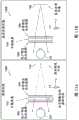
图10示出了包括一对自适应透镜组件的显示系统的示例。10 shows an example of a display system including a pair of adaptive lens assemblies.
图11A示出了图10的显示系统的示例,该显示系统在虚拟深度平面处向用户显示虚拟内容。11A shows an example of the display system of FIG. 10 displaying virtual content to a user at a virtual depth plane.
图11B示出了图10的显示系统的示例,该显示系统向用户提供真实世界内容的视图。FIG. 11B shows an example of the display system of FIG. 10 that provides a user with a view of real world content.
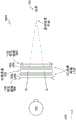
图12示出了包括一对自适应透镜组件的显示装置的示例,每个自适应透镜组件包括交替堆叠的波片透镜和可切换波片。12 shows an example of a display device including a pair of adaptive lens assemblies, each adaptive lens assembly including alternately stacked waveplate lenses and switchable waveplates.
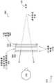
图13A和13B示出了包括一对自适应透镜组件和一对固定透镜的显示装置的示例。13A and 13B illustrate an example of a display device including a pair of adaptive lens assemblies and a pair of fixed lenses.
图14示出了包括一对自适应透镜组件和固定透镜的显示装置的示例。FIG. 14 shows an example of a display device including a pair of adaptive lens assemblies and a fixed lens.
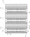
图15示出了包括三个自适应透镜层的示例自适应透镜组件。15 shows an example adaptive lens assembly including three adaptive lens layers.
图16A和16B示出了另外的示例自适应透镜组件,每一个均包括三个自适应透镜层。16A and 16B illustrate additional example adaptive lens assemblies, each including three adaptive lens layers.
图17A-17E示出了用于制造自适应透镜组件的示例过程。17A-17E illustrate an example process for fabricating an adaptive lens assembly.
图18A示出了用于采用针对自适应透镜组件的光学配向过程来卷对卷制造透镜基板的示例设备。18A shows an example apparatus for roll-to-roll manufacturing of lens substrates using an optical alignment process for an adaptive lens assembly.
图18B-C示出了用于采用针对自适应透镜组件的压印配向过程来卷对卷制造透镜基板的示例设备。18B-C illustrate example apparatus for roll-to-roll manufacturing of lens substrates using an imprint alignment process for adaptive lens assemblies.
图18D示出了用于采用针对自适应透镜组件的压印配向过程来卷对卷制造中间基板的示例设备。18D illustrates an example apparatus for roll-to-roll manufacturing of intermediate substrates using an imprint alignment process for adaptive lens assemblies.
图18E示出了用于使用由图18D的设备产生的中间基板来卷对卷制造透镜基板的示例设备。Figure 18E shows an example apparatus for roll-to-roll manufacturing of lens substrates using intermediate substrates produced by the apparatus of Figure 18D.
图19A示出了用于采用针对自适应透镜组件的压印配向过程来片材制造(sheetmanufacturing)透镜基板的示例设备。19A shows an example apparatus for sheet manufacturing a lens substrate using an imprint alignment process for an adaptive lens assembly.
图19B示出了用于采用针对自适应透镜组件的光学配向过程来板材制造透镜基板的示例设备。19B shows an example apparatus for sheet fabrication of lens substrates using an optical alignment process for adaptive lens assemblies.
图20A示出了用于采用针对自适应透镜组件的压印配向过程来旋涂制造透镜基板的示例设备。20A shows an example apparatus for spin-coating fabrication of lens substrates using an imprint alignment process for adaptive lens assemblies.
图20B示出了用于采用针对自适应透镜组件的光学配向过程来旋涂制造透镜基板的示例设备。20B shows an example apparatus for spin-coating fabrication of lens substrates using an optical alignment process for adaptive lens assemblies.
图21A-21C示出了通过定向蚀刻形成导电材料的图案的过程的示例。21A-21C illustrate an example of a process for patterning a conductive material by directional etching.
图22A-22C示出了使用溶剂可溶层形成导电材料的图案的过程的示例。22A-22C illustrate an example of a process for patterning a conductive material using a solvent-soluble layer.
图23A-23C示出了使用种子层形成导电材料的图案的过程的示例。23A-23C illustrate an example of a process for patterning a conductive material using a seed layer.
图24A-24C示出了使用种子层形成导电材料的图案的过程的另一示例。24A-24C illustrate another example of a process for patterning a conductive material using a seed layer.
图25A-25C示出了通过将金属材料的悬浮液沉积到图案化的层中的开口中来形成导电材料图案的过程的示例。25A-25C illustrate an example of a process for forming a pattern of conductive material by depositing a suspension of metallic material into openings in a patterned layer.
图26A-26F示出了导电材料的图案的俯视图的示例。26A-26F illustrate examples of top views of patterns of conductive material.
图27A-27D示出了导电材料线的剖面侧视图的示例。27A-27D illustrate examples of cross-sectional side views of lines of conductive material.
具体实施方式Detailed ways
AR系统可以将虚拟内容显示给用户或观察者,同时仍然允许用户看到其周围的世界。优选地,该内容被显示在头戴式显示器(例如,作为眼镜的一部分)上,该头戴式显示器将图像信息投射到用户的眼睛。另外,显示器还可以将来自周围环境的光透射到用户的眼睛,以允许该周围环境的视图。如本文所使用的,将理解到,“头戴式”或“可头戴式”显示器是可以安装在观察者或者用户的头部上的显示器。AR systems can display virtual content to the user or observer, while still allowing the user to see the world around them. Preferably, the content is displayed on a head-mounted display (eg, as part of glasses) that projects image information to the user's eyes. Additionally, the display may also transmit light from the surrounding environment to the user's eyes to allow a view of the surrounding environment. As used herein, it will be understood that a "head mounted" or "head mountable" display is a display that can be mounted on the head of a viewer or user.
在一些AR系统中,多个波导可被配置为在多个虚拟深度平面(在本文中也简称为“深度平面”)处形成虚拟图像。多个波导中的不同波导可具有不同的光焦度,这可提供看起来在距用户眼睛不同距离处的不同深度平面上的图像。显示系统还可包括提供光焦度或修改波导的光焦度的多个透镜。不期望地,波导和透镜中的每一个可增加显示器的整体厚度和重量。In some AR systems, multiple waveguides may be configured to form virtual images at multiple virtual depth planes (also simply referred to herein as "depth planes"). Different waveguides in the plurality of waveguides can have different optical powers, which can provide images that appear to be on different depth planes at different distances from the user's eye. The display system may also include a plurality of lenses that provide optical power or modify the optical power of the waveguide. Undesirably, each of the waveguides and lenses can add to the overall thickness and weight of the display.
在用于减小显示器的厚度和重量的方法中,已提出了自适应透镜组件,其也可称为可变聚焦透镜组件。自适应透镜组件提供可变的光焦度,以例如修改传播通过透镜组件的光的波前发散,以提供多个不同的虚拟深度平面。例如,代替多个波导,可利用单个自适应透镜组件来提供一组不同的光焦度和相关联的深度平面。自适应透镜组件和相关结构的示例在2016年11月18日提交的美国临时专利申请No.62/424,341和2017年6月12日提交的美国临时专利申请No.62/518,539中公开,在此通过引用将其全部公开并入本文。Among methods for reducing the thickness and weight of displays, adaptive lens assemblies, which may also be referred to as variable focus lens assemblies, have been proposed. The adaptive lens assembly provides variable optical power to, for example, modify the wavefront divergence of light propagating through the lens assembly to provide multiple different virtual depth planes. For example, instead of multiple waveguides, a single adaptive lens assembly can be utilized to provide a set of different optical powers and associated depth planes. Examples of adaptive lens assemblies and related structures are disclosed in US Provisional Patent Application No. 62/424,341, filed November 18, 2016, and US Provisional Patent Application No. 62/518,539, filed June 12, 2017, herein Its entire disclosure is incorporated herein by reference.
自适应透镜组件可包括自适应透镜子组件的堆叠,自适应透镜子组件中的每一个可包括波片透镜和可切换波片组件,该可切换波片组件可包括具有液晶分子的液晶层,该液晶分子可在具有不同取向的不同状态之间切换。可切换波片组件可包括:一对基板,其用于限制液晶层;配向层,其用于建立液晶层中的液晶分子的取向;以及导电层,其用于提供电场以切换液晶分子的取向。将理解到,每个自适应透镜子组件可依赖于可切换波片的状态而不同地影响通过的光的波前。多个子组件的光焦度可被组合以提供不同的总光焦度。然而,已发现具有大量这种子组件的自适应透镜组件可能仍比期望的厚。The adaptive lens assembly can include a stack of adaptive lens subassemblies, each of the adaptive lens subassemblies can include a wave plate lens and a switchable wave plate assembly, the switchable wave plate assembly can include a liquid crystal layer having liquid crystal molecules, The liquid crystal molecules can be switched between different states with different orientations. The switchable wave plate assembly may include: a pair of substrates for confining the liquid crystal layer; an alignment layer for establishing the orientation of liquid crystal molecules in the liquid crystal layer; and a conductive layer for providing an electric field to switch the orientation of the liquid crystal molecules . It will be appreciated that each adaptive lens subassembly can affect the wavefront of the light passing through differently depending on the state of the switchable waveplate. The optical powers of multiple subassemblies can be combined to provide different total optical powers. However, it has been found that adaptive lens assemblies with a large number of such subassemblies may still be thicker than desired.
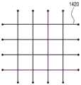
有利地,在一些实施例中,提供了薄的自适应透镜组件以及用于制造这种组件的方法和设备。在一些实施例中,可切换波片组件可包括一对本身就是波片(例如,四分之一波片)的基板,并且在它们之间设置有可切换波片(优选地,具有选择性地可切换取向的液晶分子的液晶层)。优选地,基板不包含液晶。在一些其他实施例中,可切换波片组件可包括电极的图案,该电极的图案既用作液晶分子的配向引导件,又用作选择性地建立用于切换液晶分子的取向的电场的导电层。在一些实施例中,电极图案可设置在也用作波片的基板的表面上。例如,电极可设置在基板的相对面上,并且设置在基板之间被液晶层占据的相同体积中。将理解到,电极可被自由放置在基板的表面上或者可嵌入其他材料层中。Advantageously, in some embodiments, thin adaptive lens assemblies and methods and apparatus for making such assemblies are provided. In some embodiments, a switchable wave plate assembly may include a pair of substrates that are themselves wave plates (eg, quarter wave plates), with a switchable wave plate (preferably, selective) disposed therebetween. A liquid crystal layer of liquid crystal molecules with a switchable orientation). Preferably, the substrate does not contain liquid crystals. In some other embodiments, the switchable wave plate assembly may include a pattern of electrodes that both serve as alignment guides for the liquid crystal molecules and as electrical conduction to selectively establish an electric field for switching the orientation of the liquid crystal molecules Floor. In some embodiments, electrode patterns may be provided on the surface of a substrate that also serves as a wave plate. For example, electrodes may be provided on opposite sides of the substrates and in the same volume between the substrates that is occupied by the liquid crystal layer. It will be appreciated that the electrodes may be freely placed on the surface of the substrate or may be embedded in layers of other materials.
有利地,薄的可切换波片组件可与无源波片透镜一起形成自适应透镜子组件,该无源波片透镜不包括随着上述电场的施加而改变取向的液晶分子。将理解到,可切换波片组件和无源波片透镜可改变光的偏振并进而提供光焦度。无源波片透镜可由已被锁定成特定图案和/或取向的聚合液晶分子形成。特定的图案和/取向可仅在光的窄波长范围内提供期望的光学响应。在一些实施例中,为了在更宽的波长范围上提供更多的宽带响应,可提供多个波片透镜。波片透镜中的每一个可在不同的波长范围内具有峰值响应,并且总的来说,波片透镜在更宽的波长范围内提供响应。Advantageously, a thin switchable waveplate assembly can form an adaptive lens subassembly together with a passive waveplate lens that does not include liquid crystal molecules that change orientation upon application of the aforementioned electric field. It will be appreciated that the switchable wave plate assembly and passive wave plate lens can change the polarization of light and thereby provide optical power. Passive waveplate lenses may be formed from polymeric liquid crystal molecules that have been locked into a particular pattern and/or orientation. Certain patterns and/or orientations can provide the desired optical response only within a narrow wavelength range of light. In some embodiments, multiple waveplate lenses may be provided in order to provide a more broadband response over a wider range of wavelengths. Each of the waveplate lenses can have a peak response in a different wavelength range, and collectively, the waveplate lenses provide response over a wider range of wavelengths.
如本文所述,多个子组件可堆叠在一起以形成提供一定范围的光焦度的自适应透镜组件。在一些其他实施例中,自适应透镜组件可仅包括单个子组件。As described herein, multiple subassemblies can be stacked together to form adaptive lens assemblies that provide a range of optical powers. In some other embodiments, the adaptive lens assembly may include only a single subassembly.
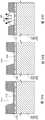
在一些实施例中,可使用卷对卷制造设备来制造自适应透镜组件或其的部分。可以将形成包含可切换液晶层的体积的部分的基板用作在其上形成相邻层的基板,然后可将一对基板放在一起以形成随后被填充有可切换液晶的体积。基板优选地由易弯曲的、机械稳定的光学透射材料形成,该材料可在制造过程期间被卷起和展开。例如,可在第一辊上提供基板的供应并且将其延伸到第二辊。基板在第一辊上展开,然后在第二辊上被重新卷起。在两者之间,可在基板上沉积并图案化配向层,并且可在配向层上沉积并固化一个或多个液晶层。优选地,供应在第一辊上的基板可包括位于基板的背侧的先前形成的电极图案。In some embodiments, roll-to-roll manufacturing equipment may be used to manufacture adaptive lens assemblies or portions thereof. The substrate forming the portion of the volume containing the switchable liquid crystal layer can be used as the substrate on which adjacent layers are formed, and a pair of substrates can then be brought together to form the volume that is subsequently filled with the switchable liquid crystal. The substrate is preferably formed from a flexible, mechanically stable, optically transmissive material that can be rolled and unrolled during the manufacturing process. For example, a supply of substrates can be provided on a first roll and extended to a second roll. The substrate is unwound on the first roll and then rewound on the second roll. In between, an alignment layer can be deposited and patterned on the substrate, and one or more liquid crystal layers can be deposited and cured on the alignment layer. Preferably, the substrate supplied on the first roller may include a previously formed electrode pattern on the backside of the substrate.
在一些实施例中,可使用第一卷对卷设备来进行配向层的制造,其中将基板卷展开并且在基板上形成压印的配向层(包括用于液晶分子的配向特征),在形成压印的配向层之后,基板卷被重新卷起。随后,第二卷对卷制造设备使用具有包括配向特征的压印配向层的基板作为起始材料、将液晶层沉积在该基板上、以及随后将具有沉积的液晶层的基板重新卷起。In some embodiments, the fabrication of the alignment layer may be performed using a first roll-to-roll apparatus in which the substrate is unrolled and an imprinted alignment layer (including alignment features for liquid crystal molecules) is formed on the substrate, After printing the alignment layer, the substrate roll is re-rolled. Subsequently, a second roll-to-roll manufacturing apparatus uses a substrate having an imprinted alignment layer including alignment features as a starting material, deposits a liquid crystal layer on the substrate, and then rewinds the substrate with the deposited liquid crystal layer.
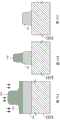
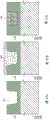
在一些实施例中,在卷对卷处理之后,可将在一侧上具有电极并且在该片材的相对侧上具有沉积层的经处理的基板片材与在另一片材的表面上具有电极的另一基板片材接合。在将基板片材接合在一起之前,可在一个或两个片材上形成用于横向限制后面的液晶填充物的壁。壁可以是用于显示器目镜所需的形状。然后,可将片材接合在一起,使电极彼此面对,以形成开放体积。该开放体积随后被液晶填充,然后可切割片材以形成单独的显示目镜。在一些其他实施例中,可在由壁和下方的基板限定的体积中提供液晶,然后可将上覆的基板粘附到壁上以形成封闭的体积。In some embodiments, after roll-to-roll processing, a treated substrate sheet having electrodes on one side and a deposited layer on the opposite side of the sheet may be combined with a sheet having electrodes on the surface of the other sheet. The other substrate sheet of the electrode is bonded. Before joining the substrate sheets together, walls may be formed on one or both sheets to laterally confine the liquid crystal fill behind. The wall may be of the desired shape for the display eyepiece. The sheets can then be joined together with the electrodes facing each other to form an open volume. This open volume is then filled with liquid crystal, and the sheet can then be cut to form individual display eyepieces. In some other embodiments, the liquid crystal can be provided in a volume defined by a wall and an underlying substrate, and an overlying substrate can then be adhered to the wall to form an enclosed volume.
有利地,在一些实施例中,本文所述的自适应透镜组件可以是薄的和/或轻的结构。例如,具有三个自适应透镜子组件的自适应透镜组件可具有相对较小的厚度(例如,在一些实施例中小于2mm)。通过使四分之一波片既用作自适应透镜子组件内的光学元件又用作支撑基板,可不需要附加的支撑基板。此外,可将四分之一波片的靠近液晶层的表面上的布线丝网或布线阵列布置成既用作电势源又用作引导液晶层中的液晶分子的配向的配向结构。另外,所公开的卷对卷制造设备和方法允许自适应透镜组件的有效、高产量制造。Advantageously, in some embodiments, the adaptive lens assemblies described herein may be thin and/or lightweight structures. For example, an adaptive lens assembly with three adaptive lens subassemblies may have a relatively small thickness (eg, less than 2 mm in some embodiments). By having the quarter wave plate serve both as an optical element within the adaptive lens subassembly and as a support substrate, no additional support substrate is required. In addition, the wiring mesh or wiring array on the surface of the quarter wave plate close to the liquid crystal layer can be arranged to serve both as a potential source and as an alignment structure for guiding the alignment of liquid crystal molecules in the liquid crystal layer. Additionally, the disclosed roll-to-roll manufacturing apparatus and method allow for efficient, high-throughput manufacturing of adaptive lens assemblies.
现在将参考附图,其中贯穿全文,相似的参考标号表示相似的部件。除非另外说明,否则附图是示意性的,不一定按比例绘制。Reference will now be made to the drawings, wherein like reference numerals refer to like parts throughout. Unless otherwise stated, the drawings are schematic and not necessarily to scale.
图2示出了用于针对用户模拟三维影像的常规显示系统。将理解到,用户的眼睛是隔开的,并且当观看空间中的真实对象时,每只眼睛将具有略微不同的对象视图,并且可以在每个眼睛的视网膜上的不同位置处形成对象的图像。这可以被称为双目视差,并且可以由人类视觉系统利用以提供深度感知。常规的显示系统通过呈现具有相同虚拟对象的略微不同视图(每只眼睛210、220一个)的两个不同图像190、200来模拟双目视差,该不同的视图对应于每只眼睛将看到的虚拟对象的视图,该虚拟对象是位于期望的深度处的真实对象的虚拟对象。这些图像提供双目提示,其中,用户的视觉系统可以解释该双目提示以得到深度感知。Figure 2 shows a conventional display system for simulating a three-dimensional imagery for a user. It will be appreciated that the user's eyes are spaced apart and when viewing a real object in space, each eye will have a slightly different view of the object, and images of the object may be formed at different locations on the retina of each eye . This can be referred to as binocular disparity, and can be exploited by the human visual system to provide depth perception. Conventional display systems simulate binocular disparity by presenting two
继续参考图2,图像190、200与眼睛210、220在z轴上隔开距离230。z轴平行于观察者的光轴,他们的眼睛注视在直接位于观察者前方的光学无限远处的对象上。图像190、200是平坦的并且在距眼睛210、220的固定距离处。基于分别呈现给眼睛210、220的图像中的虚拟对象的略微不同的视图,眼睛可以自然地旋转,使得对象的图像落在每只眼睛的视网膜上的相应点上,以维持单个双目视觉。该旋转可以使得每只眼睛210、220的视线会聚到虚拟对象被感知为存在的空间中的点上。结果,提供三维影像通常涉及提供双目提示,该双目提示可以操纵用户眼睛210、220的辐辏,并且人类视觉系统解释该双目提示以提供深度感知。With continued reference to Figure 2, the
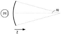
然而,产生真实且舒适的深度感知具有挑战性。将理解到,来自距眼睛不同距离处的对象的光具有不同发散量的波前。图3A-3C示了距离与光线的发散之间的关系。对象与眼睛210之间的距离以减小的距离的次序由R1、R2和R3表示。如在图3A-3C中所示,当到对象的距离减小时,光线变得更发散。相对的,当距离增加时,光线变得更准直。换句话说,可以说由点(对象或者对象的一部分)产生的光场具有球面波前曲率,该球面波前曲率是该点距用户的眼睛多远的函数。曲率随着对象与眼睛210之间的距离的减小而增加。虽然在图3A-3C和本文中的其他附图中为了说明清晰起见,仅示出单只眼睛210,关于眼睛210的讨论可以适用于观察者的两只眼睛210和220。However, generating realistic and comfortable depth perception is challenging. It will be appreciated that light from objects at different distances from the eye has different diverging wavefronts. 3A-3C illustrate the relationship between distance and divergence of light. The distances between the subject and the
继续参考图3A-3C,来自观察者的眼睛注视到的对象的光可以具有不同程度的波前发散。由于波前发散的量不同,光可以通过眼睛的晶状体而被不同地聚焦,这进而可能需要晶状体呈现不同的形状以在眼睛的视网膜上形成聚焦的图像。在视网膜上没有形成聚焦的图像的情况下,所产生的视网膜模糊充当调节的提示,该调节引起眼睛的晶状体形状的改变,直到在视网膜上形成聚焦的图像。例如,对调节的提示可以触发眼睛晶状体周围的睫状肌松弛或收缩,从而调节施加到保持晶状体的悬韧带的力,由此使眼睛晶状体的形状改变直到注视的对象的视网膜模糊消除或最小化,从而在眼睛的视网膜(例如,中央凹)上形成注视对象的聚焦的图像。眼睛的晶状体改变形状的过程可以称为调节,以及在眼睛的视网膜(例如,中央凹)上形成注视对象的聚焦的图像所需的眼睛的晶状体的形状可以称为调节状态。With continued reference to Figures 3A-3C, light from an object to which an observer's eyes are looking may have varying degrees of wavefront divergence. Due to the different amounts of wavefront divergence, light can be focused differently through the lens of the eye, which in turn may require the lens to assume a different shape to form a focused image on the retina of the eye. In the absence of a focused image forming on the retina, the resulting retinal blur acts as a cue for accommodation that causes changes in the shape of the eye's lens until a focused image is formed on the retina. For example, a cue to accommodate can trigger relaxation or contraction of the ciliary muscles surrounding the eye's lens, thereby adjusting the force applied to the suspensory ligament that holds the lens, thereby causing the eye's lens to change shape until retinal blurring of the staring object is eliminated or minimized , thereby forming a focused image of the gazing object on the retina of the eye (eg, the fovea). The process by which the eye's lens changes shape may be referred to as accommodation, and the shape of the eye's lens required to form a focused image of a gazing object on the eye's retina (eg, fovea) may be referred to as the accommodation state.
现在参考图4A,示出了人类视觉系统的调节-辐辏响应的表示。眼睛运动以注视对象使得眼睛接收来自对象的光,其中光在眼睛的视网膜中的每一个上形成图像。在视网膜上形成的图像中视网膜模糊的存在可以提供对调节的提示,并且图像在视网膜上的相对位置可以提供对辐辏的提示。对调节的提示引起调节发生,导致眼睛的晶状体各自呈现特定的调节状态,该特定的调节状态在眼睛的视网膜(例如,中央凹)上形成对象的聚焦的图像。另一方面,对辐辏的提示引起辐辏运动(眼睛的旋转)发生,使得在每只眼睛的每个视网膜上形成的图像处于维持单个双目视觉的相应视网膜点处。在这些位置,可以说眼睛已处于特定的辐辏状态。继续参考图4A,调节可以被理解为眼睛实现特定调节状态的过程,以及辐辏可以被理解为眼睛实现特定辐辏状态的过程。如图4A中所示,如果用户注视另一个对象,则眼睛的调节和辐辏状态可以改变。例如,如果用户注视在z轴上的不同深度处的新对象,则调节状态可以改变。Referring now to FIG. 4A, a representation of the accommodation-vergence response of the human visual system is shown. The movement of the eye to look at the object causes the eye to receive light from the object, where the light forms an image on each of the retinas of the eye. The presence of retinal blur in images formed on the retina may provide cues for accommodation, and the relative position of the images on the retina may provide cues for convergence. A cue to accommodation causes accommodation to occur, causing the lenses of the eye to each assume a specific accommodation state that forms a focused image of the subject on the retina (eg, fovea) of the eye. On the other hand, cues to vergence cause vergence motion (rotation of the eye) to occur such that the image formed on each retina of each eye is at the corresponding retinal point that maintains single binocular vision. In these positions, the eye can be said to be in a specific state of vergence. With continued reference to Figure 4A, accommodation can be understood as the process by which the eye achieves a particular state of accommodation, and vergence can be understood as the process by which the eye achieves a particular state of convergence. As shown in Figure 4A, if the user is gazing at another object, the accommodation and vergence states of the eyes may change. For example, if the user gazes at a new object at a different depth on the z-axis, the accommodation state may change.
不受理论的限制,据信对象的观察者可以由于辐辏和调节的组合而将对象感知为“三维的”。如上所述,两只眼睛相对于彼此的辐辏运动(例如,眼睛的转动使得瞳孔向着彼此或远离彼此运动以会聚眼睛的视线来注视对象)与眼睛的晶状体的调节紧密相关。在正常情况下,改变眼睛的晶状体的形状以将聚焦从一个对象改变到位于不同距离处的另一对象,将会在被称为“调节-辐辏反射”的关系下自动引起到相同距离的辐辏的匹配变化。同样,在正常情况下,辐辏的变化将引发晶状体形状的匹配变化。Without being bound by theory, it is believed that an observer of an object may perceive the object as "three-dimensional" due to a combination of vergence and accommodation. As discussed above, the vergence movement of the two eyes relative to each other (eg, the rotation of the eyes to move the pupils toward or away from each other to converge the eyes of the eyes to fixate on objects) is closely related to the accommodation of the lenses of the eyes. Under normal circumstances, changing the shape of the eye's lens to change focus from one object to another at a different distance will automatically induce a vergence to the same distance in a relationship known as the "accommodation-vergence reflex" matching changes. Also, under normal circumstances, changes in vergence will trigger matching changes in lens shape.
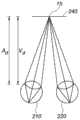
现在参考图4B,示出了眼睛的不同调节和辐辏状态的示例。眼睛对222a注视在光学无穷远处的对象上,而眼睛对222b注视在小于光学无限远处的对象221上。值得注意的是,每对眼睛的辐辏状态不同,其中眼睛对222a指向正前方,而眼睛对222会聚在对象221上。形成每个眼睛对222a和222b的眼睛的调节状态是也可以不同,如晶状体210a、220a的不同形状所表示的。Referring now to Figure 4B, examples of different accommodation and vergence states of the eye are shown.
不希望的是,常规“3-D”显示系统的许多用户发现由于这些显示器中的调节和辐辏状态之间的不匹配这些常规系统不舒服或者根本不会感知到深度感。如上所述,许多立体或“3-D”显示系统通过向每只眼睛提供略微不同的图像来显示场景。这样的系统对于许多观察者来说不舒服,因为它们除了其他事项之外仅仅提供场景的不同呈现并且引起眼睛的辐辏状态的改变,但是没有那些眼睛的相应的调节状态的改变。然而,图像由距眼睛固定距离处的显示器示出,使得眼睛在单个调节状态下观看所有图像信息。这种布置通过引起辐辏状态的变化而没有调节状态的匹配变化来违背“调节-辐辏反射”。这种不匹配被认为会引起观察者的不适。提供调节和辐辏之间的更好匹配的显示系统可以形成更真实和舒适的三维影像模拟。Undesirably, many users of conventional "3-D" display systems find these conventional systems uncomfortable or do not perceive depth at all due to the mismatch between accommodation and vergence states in these displays. As mentioned above, many stereoscopic or "3-D" display systems display scenes by presenting slightly different images to each eye. Such systems are uncomfortable for many observers because, among other things, they merely provide a different representation of the scene and cause changes in the vergence states of the eyes, but not the corresponding accommodation states of those eyes. However, the image is shown by the display at a fixed distance from the eye so that the eye sees all image information in a single accommodation state. This arrangement violates the "accommodation-vergence reflex" by causing a change in the vergence state without a matching change in the accommodation state. This mismatch is thought to cause discomfort to the observer. A display system that provides a better match between accommodation and vergence can result in a more realistic and comfortable three-dimensional image simulation.
不受理论限制,据信人眼通常可解释有限数量的深度平面以提供深度感知。因此,通过向眼睛提供与这些有限数量的深度平面中的每一个相对应的图像的不同呈现,可实现高度可信的感知深度的模拟。在一些实施例中,不同的呈现可提供对辐辏的提示和对调节的匹配提示,从而提供生理上正确的调节-辐辏匹配。Without being bound by theory, it is believed that the human eye can generally interpret a limited number of depth planes to provide depth perception. Thus, by providing the eye with different representations of images corresponding to each of these limited number of depth planes, a highly confident simulation of perceived depth can be achieved. In some embodiments, different presentations may provide cues for vergence and matching cues for accommodation, thereby providing a physiologically correct accommodation-vergence match.
继续参考图4B,示出了两个深度平面240,其对应于在空间中距眼睛210、220的不同距离。对于给定的深度平面240,可以通过为每只眼睛210、220显示适当不同透视的图像来提供辐辏提示。此外,对于给定的深度平面240,形成提供给每只眼睛210、220的图像的光可以具有与由该深度平面240的距离处的点产生的光场对应的波前发散。With continued reference to Figure 4B, two
在所示实施例中,包含点221的深度平面240沿z轴的距离是1m。如本文所使用的,可以通过位于用户眼睛的出射光瞳处的零点来测量沿z轴的距离或深度。因此,在眼睛指向光学无限远那些眼睛的光轴上,位于1m深度处的深度平面240与距用户眼睛的出射光瞳1m的距离对应。作为近似,沿着z轴的深度或距离可以从用户眼睛前方的显示器(例如,从波导的表面)测量,加上装置和用户眼睛的出射光瞳之间的距离的值。该值可以被称为视距(eyerelief)并且对应于用户眼睛的出射光瞳与用户在眼睛前方佩戴的显示器之间的距离。在实践中,视距的值可以是通常对于所有观察者使用的标准化值。例如,可以假设视距是20mm,以及深度为1m的深度平面可以在显示器前方980mm的距离处。In the illustrated embodiment, the distance along the z-axis of the
现在参考图4C和4D,分别示出了匹配的调节-辐辏距离和不匹配的调节-辐辏距离的示例。如图4C所示,显示系统可以向每只眼睛210、220提供虚拟对象的图像。图像可以使眼睛210、220呈现眼睛会聚在深度平面240上的点15上的辐辏状态。此外,图像可以由具有与该深度平面240处的真实对象相对应的波前曲率的光形成。结果,眼睛210、220呈现图像在那些眼睛的视网膜上合焦的调节状态。因此,用户可以感知到虚拟对象在深度平面240上的点15处。Referring now to Figures 4C and 4D, examples of matched accommodation-convergence distances and unmatched accommodation-convergence distances are shown, respectively. As shown in Figure 4C, the display system may provide each
将理解到,眼睛210、220的调节和辐辏状态中的每一者与z轴上的特定距离相关联。例如,距眼睛210、220特定距离处的对象使得那些眼睛基于对象的距离呈现特定的调节状态。与特定调节状态相关联的距离可以被称为调节距离Ad。类似地,存在与在特定辐辏状态下的眼睛或相对于彼此的位置相关联的特定的辐辏距离Vd。在调节距离和辐辏距离匹配的情况下,可以说调节和辐辏之间的关系在生理学上是正确的。这被认为是对观众最舒适的场景。It will be appreciated that each of the accommodation and vergence states of the
然而,在立体显示器中,调节距离和辐辏距离可能不总是匹配。例如,如图4D所示,显示给眼睛210、220的图像可以以对应于深度平面240的波前发散而被显示,并且眼睛210、220可以呈现在该深度平面上的点15a、15b合焦的特定的调节状态。然而,显示给眼睛210、220的图像可能提供使眼睛210、220会聚在不位于深度平面240上的点15的对辐辏的提示。结果,在一些实施例中,调节距离对应于从眼睛210、220的出射光瞳到深度平面240的距离,而辐辏距离对应于从眼睛210、220的出射光瞳到点15的更大距离。调节距离与辐辏距离不同。因此,存在调节-辐辏不匹配。这种不匹配被认为是不期望的并且可能引起用户的不适。将理解到,不匹配对应于距离(例如,Vd-Ad)并且可以使用屈光度来表征。However, in stereoscopic displays, accommodation distance and vergence distance may not always match. For example, as shown in Figure 4D, images displayed to
在一些实施例中,将理解到,除了眼睛210、220的出射光瞳之外的参考点可以用来确定用于确定调节-辐辏不匹配的距离,只要相同的参考点用于调节距离和辐辏距离即可。例如,可以从角膜到深度平面、从视网膜到深度平面、从目镜(例如,显示装置的波导)到深度平面等来测量距离。In some embodiments, it will be appreciated that reference points other than the exit pupils of
不受理论的限制,据信用户仍然可以感知作为在生理上是正确的高达约0.25屈光度、高达约0.33屈光度和高达约0.5屈光度的调节-辐辏不匹配,而没有不匹配本身引起的显著的不适。在一些实施例中,本文公开的显示系统(例如,图6的显示系统250)向观察者呈现具有约0.5屈光度或更小的调节-辐辏不匹配的图像。在一些其他实施例中,由显示系统提供的图像的调节-辐辏不匹配为约0.33屈光度或更小。在其他实施例中,由显示系统提供的图像的调节-辐辏不匹配为约0.25屈光度或更小,包括约0.1屈光度或更小。Without being bound by theory, it is believed that a user can still perceive accommodation-convergence mismatches as physiologically correct up to about 0.25 diopters, up to about 0.33 diopters, and up to about 0.5 diopters without the significant discomfort caused by the mismatch itself . In some embodiments, a display system disclosed herein (eg,
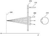
图5示出了通过修改波前发散来模拟三维影像的方法的方面。该显示系统包括波导270,该波导270被配置为接收利用图像信息编码的光770并将该光输出到用户的眼睛210。波导270可以输出具有与由期望深度平面240上的点产生的光场的波前发散相对应的限定量的波前发散的光650。在一些实施例中,为在该深度平面上呈现的所有对象提供相同量的波前发散。另外,将说明可以向用户的另一只眼睛提供来自类似波导的图像信息。Figure 5 illustrates aspects of a method of simulating three-dimensional imagery by modifying wavefront divergence. The display system includes a
在一些实施例中,单个波导可以被配置为以与单个或有限数量的深度平面对应的设定量的波前发散输出光和/或波导可以被配置为输出有限波长范围的光。因此,在一些实施例中,可以利用多个波导或波导堆叠来为不同的深度平面提供不同量的波前发散和/或输出具有不同波长范围的光。如本文所使用的,将理解到,在深度平面处可以遵循平坦或弯曲表面的轮廓。在一些实施例中,有利地为了简单起见,深度平面可以遵循平坦表面的轮廓。In some embodiments, a single waveguide may be configured to output light with a set amount of wavefront divergence corresponding to a single or limited number of depth planes and/or a waveguide may be configured to output a limited wavelength range of light. Thus, in some embodiments, multiple waveguides or stacks of waveguides may be utilized to provide different amounts of wavefront divergence for different depth planes and/or output light having different wavelength ranges. As used herein, it will be understood that the contour of a flat or curved surface may be followed at the depth plane. In some embodiments, the depth plane may follow the contour of a flat surface, advantageously for simplicity.
图6示出了用于向用户输出图像信息的波导堆叠的示例。显示系统250包括波导的堆叠或者堆叠波导组件260,该波导的堆叠或者堆叠波导组件260可以用于使用多个波导270、280、290、300、310向眼睛/大脑提供三维感知。将理解到,在一些实施例中,显示系统250可以被认为是光场显示器。另外,波导组件260还可被称为目镜。Figure 6 shows an example of a waveguide stack for outputting image information to a user.
在一些实施例中,显示系统250可以被配置为提供关于辐辏的基本上连续的提示以及关于适应的多个离散的提示。可以通过向用户的每只眼睛显示不同的图像来提供对辐辏的提示,并且可以通过以可选择的离散量的波前发散输出形成图像的光来提供对调节的提示。换句话说,显示系统250可以被配置为以可变水平的波前发散输出光。在一些实施例中,波前发散的每个离散水平对应于特定深度平面并且可以由波导270、280、290、300、310中的特定一者来提供。In some embodiments, the
继续参考图6,波导组件260还可以包括波导之间的多个特征320、330、340、350。在一些实施例中,特征320、330、340、350可以是一个或多个透镜。波导270、280、290、300、310和/或多个透镜320、330、340、350可以被配置为以不同水平的波前曲率或者光线发散向眼睛发送图像信息。每个波导水平可以与特定深度平面相关联并且可以被配置为输出对应于该深度平面的图像信息。图像注入装置360、370、380、390、400可以用作用于波导的光源并且可以用于将图像信息注入波导270、280、290、300、310中,如本文所描述的,其中的每一个波导可以被配置为跨每个相应波导分布入射光,用于朝向眼睛210输出。光离开图像注入装置360、370、380、390、400的输出表面410、420、430、440、450并且注入波导270、280、290、300、310的对应的输入表面460、470、480、490、500中。在一些实施例中,输入表面460、470、480、490、500中的每一个可以是对应的波导的边缘,或者可以是对应的波导的主要表面的一部分(即,波导表面中的直接面对世界510或者观察者的眼睛210的一个表面)。在一些实施例中,单个光束(例如,准直束)可以被注入每个波导中,以输出克隆的准直束的整个场,该克隆的准直束以对应于与特定波导相关联的深度平面的特定角(和发散量)朝向眼睛210引导。在一些实施例中,图像注入装置360、370、380、390、400中的单独一个可以与多个(例如,三个)波导270、280、290、300、310相关联并且将光注入多个(例如,三个)波导270、280、290、300、310中。With continued reference to Figure 6, the
在一些实施例中,图像注入装置360、370、380、390、400是分立显示器,该分立显示器各自产生用于分别注入对应的波导270、280、290、300、310中的图像信息。在一些其他实施例中,图像注入装置360、370、380、390、400是单个复用显示器的输出端,该单个复用显示器的输出端可以例如经由一个或多个光学导管(诸如光纤光缆)将图像信息输送到图像注入装置360、370、380、390、400中的每一个。将理解到,由图像注入装置360、370、380、390、400提供的图像信息可以包括不同的波长或者颜色(例如,不同的分量颜色,如本文所讨论的)的光。In some embodiments, the
在一些实施例中,注入波导270、280、290、300、310中的光由光投射器系统520提供,该光投射器系统520包括光模块530,该光模块530可以包括光发射器,诸如发光二极管(LED)。来自光模块530的光可以经由分束器550引导到光调制器540(例如,空间光调制器)并由光调制器540修改。光调制器540可以被配置为改变注入波导270、280、290、300、310中的光的感知强度,以对具有图像信息的光编码。空间光调制器的示例包括液晶显示器(LCD),其包括硅上液晶(LCOS)显示器。将理解到,图像注入装置360、370、380、390、400被示意性地示出,并且在一些实施例中,这些图像注入装置可以表示在共用投射系统中的不同光路径和位置,该共用投射系统被配置为将光输出到波导270、280、290、300、310中的相关联的波导中。在一些实施例中,波导组件260的波导可以用作理想透镜,同时将注入波导的光中继出来到用户的眼睛。在该构思中,对象可以是空间光调制器540,以及图像可以是深度平面上的图像。In some embodiments, the light injected into the
在一些实施例中,显示系统250可以是扫描光纤显示器,其包括被配置为以各种图案(例如,光栅扫描、螺旋扫描、李沙育(Lissajous)图案等)将光投射到一个或多个波导270、280、290、300、310中并且最终到观察者的眼睛310的一个或多个扫描光纤。在一些实施例中,所图示的图像注入装置360、370、380、390、400可以示意性地表示被配置为将光注入一个或多个波导270、280、290、300、310中的单个扫描光纤或一束扫描光纤。在一些其他实施例中,所图示的图像注入装置360、370、380、390、400可以示意性地表示多个扫描光纤或多束扫描光纤,其中的每一个被配置为将光注入波导270、280、290、300、310中的相关联的一个。将理解到,一个或多个光纤可以被配置为将光从光模块530传输到一个或多个波导270、280、290、300、310。将理解到,一个或多个中间光学结构可以在扫描光纤或光纤与一个或多个波导270、280、290、300、310之间提供,以例如将离开扫描光纤的光重定向到一个或多个波导270、280、290、300、310。In some embodiments,
控制器560控制堆叠波导组件260中的一个或多个的操作,包括图像注入装置360、370、380、390、400、光源530和光调制器540的操作。在一些实施例中,控制器560是本地数据处理模块140的一部分。控制器560包括根据例如本文所公开的各种方案中的任一个调控到波导270、280、290、300、310的图像信息的时序和提供的编程(例如,非暂态介质中的指令)。在一些实施例中,控制器可以是单个积分装置,或者由有线或无线通信信道连接的分布式系统。在一些实施例中,控制器560可以是处理模块140或150(图9D)的一部分。The
继续参考图6,波导270、280、290、300、310可以被配置为通过全内反射(TIR)在每个相应波导内传播光。波导270、280、290、300、310可以各自是平面的或者具有另外的形状(例如,弯曲的),其具有主顶面和主底面以及在那些主顶面与主底面之间延伸的边缘。在所图示的配置中,波导270、280、290、300、310可以各自包括耦出光学元件570、580、590、600、610,该耦出光学元件570、580、590、600、610被配置为通过将在每个相应波导内传播的光重定向出波导来将光提取出波导,以向眼睛210输出图像信息。提取的光还可以称为耦出光,并且耦出光学元件光还可以称为光提取光学元件。所提取的光束可以由波导在波导中传播的光撞击光提取光学元件的位置处输出。耦出光学元件570、580、590、600、610可以例如是包括衍射光学特征的光栅,如本文进一步讨论的。虽然图示被设置在波导270、280、290、300、310的底主表面处以便于描述和附图清晰,但是在一些实施例中,耦出光学元件570、580、590、600、610可以设置在顶和/或底主表面处,和/或可以直接设置在波导270、280、290、300、310的体积中,如本文进一步讨论的。在一些实施例中,耦出光学元件570、580、590、600、610可以在附接到透明基板以形成波导270、280、290、300、310的材料层中形成。在一些其他实施例中,波导270、280、290、300、310可以是单片材料,并且耦出光学元件570、580、590、600、610可以在该片材料的表面上和/或内部中形成。With continued reference to Figure 6, the
继续参考图6,如本文所讨论的,每个波导270、280、290、300、310被配置为输出光以形成对应于特定深度平面的图像。例如,最靠近眼睛的波导270可以被配置为将准直光(其被注入这样的波导270中)递送给眼睛210。准直光可以表示光学无限远焦平面。下一上方波导280可以被配置为发送出准直光,该准直光在其可以到达眼睛210之前穿过第一透镜350(例如,负透镜);这样的第一透镜350可以被配置为产生轻微的凸波前曲率,使得眼睛/大脑将来自该下一上方波导280的光解释为来自从光学无限远朝向眼睛210向内更接近的第一焦平面。类似地,第三上方波导290使其输出光在到达眼睛210之前穿过第一透镜350和第二透镜340;第一透镜350和第二透镜340的组合光焦度可以被配置为产生波前曲率的另一增加量,使得眼睛/大脑将来自第三波导290的光解释为来自第二焦平面,该第二焦平面比来自下一上方波导280的光从光学无限远朝向人向内更加接近。With continued reference to Figure 6, as discussed herein, each
其他波导层300、310和透镜330、320类似地配置,其中,该堆叠中的最高波导310发送其输出通过其与眼睛之间的所有透镜,用于表示距人最近的焦平面的总光焦度。为了补偿当观看/解释来自堆叠波导组件260的另一侧的世界510的光时透镜320、330、340、350的堆叠,补偿透镜层620可以被设置在堆叠的顶部以补偿下面透镜堆叠320、330、340、350的总光焦度。这样的配置提供与存在可用的波导/透镜配对一样多的焦平面。波导的耦出光学元件和透镜的聚焦方面二者可以是静态的(即,非动态或电活性的)。在一些可选实施例中,一者或二者可以使用电活性特征是动态的。The
在一些实施例中,波导270、280、290、300、310中的两个或两个以上可以具有相同的相关联深度平面。例如,多个波导270、280、290、300、310可以被配置为将图像集输出给相同的深度平面,或者波导270、280、290、300、310的多个子集可以被配置为将图像集输出给相同的多个深度平面,其中,针对每个深度平面具有一个集。这可以提供用于形成拼接图像以在那些深度平面处提供扩展视场的优点。In some embodiments, two or more of the
继续参考图6,耦出光学元件570、580、590、600、610可以被配置为将光重定向到其相应波导之外,并且以针对与波导相关联的特定深度平面的适当的发散或准直量输出该光。因此,具有不同的相关联的深度平面的波导可以具有耦出光学元件570、580、590、600、610的不同配置,其取决于相关联的深度平面输出具有不同的发散量的光。在一些实施例中,光提取光学元件570、580、590、600、610可以是体积或者表面特征,其可以被配置为以特定角输出光。例如,光提取光学元件570、580、590、600、610可以是体积全息图、表面全息图和/或衍射光栅。在一些实施例中,特征320、330、340、350可以不是透镜;相反,它们可以简单地是间隔器(例如,包层和/或用于形成空隙的结构)。With continued reference to Figure 6, outcoupling
在一些实施例中,耦出光学元件570、580、590、600、610是形成衍射图案的衍射特征,或者“衍射光学元件”(在本文中还被称为“DOE”)。优选地,DOE具有足够低的衍射效率,使得光束的仅一部分通过DOE的每个交点朝向眼睛210偏转离开,而剩余部分继续经由TIR移动通过波导。携带图像信息的光因此被分成在许多位置处离开波导的许多相关出射束,并且结果是针对在波导内到处反弹的该特定准直束的朝向眼睛210的出射发射的相当均匀的图案。In some embodiments, outcoupling
在一些实施例中,一个或多个DOE可以在其主动地衍射的“开启”状态与其不显著地衍射的“关闭”状态之间切换。例如,可切换DOE可以包括聚合物分散液晶层,其中,微滴包括主介质中的衍射图案,并且微滴的折射率可以被切换为基本上匹配主材料的折射率(在该情况下,图案未明显地衍射入射光)或者微滴可以被切换到不匹配主介质的折射率的折射率(在该情况下,图案主动地衍射入射光)。In some embodiments, one or more DOEs can be switched between an "on" state in which they diffract actively and an "off" state in which they diffract insignificantly. For example, the switchable DOE may comprise a polymer dispersed liquid crystal layer, wherein the droplets comprise a diffraction pattern in the host medium, and the index of refraction of the droplets can be switched to substantially match the index of refraction of the host material (in which case the pattern The incident light is not significantly diffracted) or the droplets can be switched to an index of refraction that does not match the index of refraction of the host medium (in which case the pattern actively diffracts the incident light).
在一些实施例中,相机组件630(例如,数字相机,包括可见光和红外光相机)可以被提供以采集眼睛210和/或眼睛210周围的组织的图像,以例如检测用户输入和/或监测用户的生理状态。如本文所使用的,相机可以是任何图像采集装置。在一些实施例中,相机组件630可以包括图像采集装置和向眼睛投射光(例如,红外光)的光源,该光然后可以由眼睛反射并且由图像采集装置检测。在一些实施例中,相机组件630可以附接到框架80(图9D)并且可以与处理模块140和/或150电气通信,该处理模块140和/或150可以处理来自相机组件630的图像信息。在一些实施例中,可以针对每只眼睛利用一个相机组件630,以单独监测每只眼睛。In some embodiments, a camera assembly 630 (eg, a digital camera, including visible light and infrared light cameras) may be provided to acquire images of the
现在参考图7,示出了由波导输出的出射束的示例。图示了一个波导,但是将理解到,在波导组件260包括多个波导的情况下,波导组件260(图6)中的其他波导可以类似地运行。光640在波导270的输入表面460处被注入波导270中并且通过TIR在波导270内传播。在光640入射在DOE 570上的点处,光的一部分作为出射束650离开波导。出射束650被图示为基本上平行的,但是如本文所讨论的,其还可以被重定向为以某个角度传播到眼睛210(例如,形成发散出射束),这取决于与波导270相关联的深度平面。将理解到,基本上平行出射束可以指示具有耦出光学元件的波导,该耦出光学元件耦出光以形成看起来设定在距眼睛210大距离(例如,光学无限远)的深度平面上的图像。其他波导或者其他耦出光学元件集可以输出更发散的出射束图案,该出射束图案将要求眼睛210调节到更近的距离以使其对焦于视网膜并且将由大脑解释为来自比光学无限远更接近于眼睛210的距离的光。Referring now to Figure 7, an example of the exit beam output by the waveguide is shown. One waveguide is illustrated, but it will be appreciated that where
在一些实施例中,全色图像可以通过重叠分量颜色(例如,三种或更多种分量颜色)中的每一种的图像在每个深度平面处形成。图8图示了每个深度平面包括使用多种不同的分量颜色形成的图像的堆叠波导组件的示例。所图示的实施例示出深度平面240a–240f,尽管还预期了更多或更少的深度。每个深度平面可以具有与其相关联的三个或更多个分量颜色图像,包括:第一颜色G的第一图像;第二颜色R的第二图像;以及第三颜色B的第三图像。通过字母G、R和B之后的用于屈光度(dpt)的不同的数字在附图中指示不同的深度平面。仅作为示例,这些字母中的每一个之后的数字指示屈光度(1/m),或者深度平面距观察者的反距离,并且附图中的每个框表示单个分量颜色图像。在一些实施例中,为了解释不同的波长的光的眼睛聚焦的差异,用于不同的颜色分量的深度平面的确切定位可以变化。例如,对于给定深度平面的不同的分量颜色图像可以被放置在对应于距用户不同距离的深度平面上。这样的布置可以增加视觉灵敏度和用户舒适和/或可以减小色差。In some embodiments, a full-color image may be formed at each depth plane by overlapping images of each of the component colors (eg, three or more component colors). 8 illustrates an example of a stacked waveguide assembly in which each depth plane includes images formed using multiple different component colors. The illustrated embodiment shows
在一些实施例中,每种分量颜色的光可以由单个专用波导输出,并且因此,每个深度平面可以具有与其相关联的多个波导。在这样的实施例中,包括字母G、R或B的图中的每个框可以被理解为表示单独波导,并且每深度平面可以提供三个波导,其中,每深度平面提供三种分量颜色图像。虽然与每个深度平面相关联的波导在该附图中被示出为彼此邻近,但是将理解到,在物理设备中,波导可以全部布置在堆叠中,其中,每层具有一个波导。在一些其他实施例中,多种分量颜色可以由相同波导输出,使得例如,每深度平面可以仅提供单个波导。In some embodiments, light of each component color may be output by a single dedicated waveguide, and thus, each depth plane may have multiple waveguides associated with it. In such an embodiment, each box in a figure including the letter G, R or B may be understood to represent a separate waveguide, and three waveguides may be provided per depth plane, wherein each depth plane provides three component color images . Although the waveguides associated with each depth plane are shown adjacent to each other in this figure, it will be appreciated that in a physical device, the waveguides may all be arranged in a stack, with one waveguide per layer. In some other embodiments, multiple component colors may be output by the same waveguide, such that, for example, only a single waveguide may be provided per depth plane.
继续参考图8,在一些实施例中,G是绿色,R是红色,并且B是蓝色。在一些其他实施例中,与光的其他波长相关联的其他颜色(包括品红和青色)可以另外使用或者可以替换红、绿或蓝中的一个或多个。With continued reference to Figure 8, in some embodiments, G is green, R is red, and B is blue. In some other embodiments, other colors associated with other wavelengths of light, including magenta and cyan, may be used in addition or may replace one or more of red, green, or blue.
将理解到,贯穿本公开对于给定的光颜色的引用将被理解为涵盖由观察者感知为具有该给定颜色的光的波长的范围内的一个或多个波长的光。例如,红光可以包括大约620–780nm的范围内的一个或多个波长的光,绿光可以包括大约492–577nm的范围内的一个或多个波长的光,并且蓝光可以包括大约435–493nm的范围内的一个或多个波长的光。It will be appreciated that references throughout this disclosure to a given color of light will be understood to encompass one or more wavelengths of light within a range of wavelengths of light perceived by an observer as having that given color. For example, red light may include one or more wavelengths of light in the range of approximately 620-780 nm, green light may include one or more wavelengths of light in the range of approximately 492-577 nm, and blue light may include approximately 435-493 nm A range of one or more wavelengths of light.
在一些实施例中,光源530(图6)可以被配置为发射观察者的视觉感知范围之外的一个或多个波长的光,例如,红外和/或紫外波长。另外,显示器250的波导的耦入、耦出和其他光重定向结构可以被配置为朝向用户的眼睛210将该光引导并且发射到显示器之外,例如,用于成像和/或用户刺激应用。In some embodiments, light source 530 (FIG. 6) may be configured to emit light at one or more wavelengths outside the visual perception range of an observer, eg, infrared and/or ultraviolet wavelengths. Additionally, the coupling in, outcoupling, and other light redirecting structures of the waveguides of the
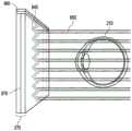
现在参考图9A,在一些实施例中,入射在波导上的光可能需要重定向以将该光耦入到波导中。耦入光学元件可以用于将光重定向并且耦入到其对应的波导中。图9A图示了各自包括耦入光学元件的多个堆叠波导或堆叠波导集660的示例的剖面侧视图。波导可以各自被配置为输出一个或多个不同波长或者一个或多个不同波长范围的光。将理解到,堆叠660可以对应于堆叠260(图6),并且所图示的堆叠660的波导可以对应于多个波导270、280、290、300、310的一部分,例外的是,来自图像注入装置360、370、380、390、400中的一个或多个的光从期望光重定向以耦入的位置被注入到波导中。Referring now to FIG. 9A, in some embodiments, light incident on a waveguide may need to be redirected to couple the light into the waveguide. In-coupling optics can be used to redirect and couple light into its corresponding waveguide. 9A illustrates a cross-sectional side view of an example of a plurality of stacked waveguides or sets of
所图示的堆叠波导集660包括波导670、680和690。每个波导包括相关联的耦入光学元件(其还可以被称为波导上的光输入区),其中例如,在波导670的主表面(例如,上主表面)上设置的耦入光学元件700、在波导680的主表面(例如,上主表面)上设置的耦入光学元件710,以及在波导690的主表面(例如,上主表面)上设置的耦入光学元件720。在一些实施例中,耦入光学元件700、710、720中的一个或多个可以设置在相应波导670、680、690的底主表面上(特别地,其中,一个或多个耦入光学元件是反射偏转光学元件)。如所图示的,耦入光学元件700、710、720可以被设置在其相应波导670、680、690的上主表面上(或在下一个较低波导的顶部),特别地,其中,那些耦入光学元件是透射偏转光学元件。在一些实施例中,耦入光学元件700、710、720可以被设置在相应波导670、680、690的本体中。在一些实施例中,如本文所讨论的,耦入光学元件700、710、720是波长选择的,使得其选择性地重定向光的一个或多个波长,同时透射光的其他波长。虽然图示在其相应波导670、680、690的一个边或角上,但是将理解到,在一些实施例中,耦入光学元件700、710、720可以设置在其相应波导670、680、690的其他区域中。The illustrated
如所图示的,耦入光学元件700、710、720可以彼此横向偏移。在一些实施例中,每个耦入光学元件可以偏移,使得其在该光不穿过另一耦入光学元件的情况下接收光。例如,每个耦入光学元件700、710、720可以被配置为从如图6中所示的不同图像注入装置360、370、380、390和400接收光,并且可以与其他耦入光学元件700、710、720分离(例如,横向地隔开),使得其基本上不接收来自耦入光学元件700、710、720中的其他耦入光学元件的光。As illustrated, the in-coupling
每个波导还包括相关联的光分布元件,例如,在波导670的主表面(例如,顶主表面)上设置的光分布元件730、在波导680的主表面(例如,顶主表面)上设置的光分布元件740,以及在波导690的主表面(例如,顶主表面)上设置的光分布元件750。在一些其他实施例中,光分布元件730、740、750可以分别设置在相关联的波导670、680、690的底主表面上。在一些其他实施例中,光分布元件730、740、750可以分别设置在相关联的波导670、680、690的顶主表面和底主表面上;或者光分布元件730、740、750可以分别设置在不同的相关联的波导670、680、690中的顶主表面和底主表面中的不同的主表面上。Each waveguide also includes an associated light distributing element, eg, light distributing
波导670、680、690可以通过例如气体、液体和/或固态材料层隔开并分离。例如,如所图示的,层760a可以将波导670和680分离;并且层760b可以将波导680和690分离。在一些实施例中,层760a和760b由低折射率材料(即,具有比形成波导670、680、690中的直接相邻的一个波导的材料更低的折射率的材料)形成。优选地,形成层760a、760b的材料的折射率小于形成波导670、680、690的材料的折射率0.05或更多,或者0.10或更少。有利地,较低折射率层760a、760b可以用作包层,该包层利于通过波导670、680、690的光的全内反射(TIR)(例如,每个波导的顶主表面与底主表面之间的TIR)。在一些实施例中,层760a、760b由空气形成。虽然未图示,但是将理解到,所图示的波导集660的顶部和底部可以包括直接邻近的包层。The
优选地,为了便于制造和其他考虑,形成波导670、680、690的材料类似或者相同,并且形成层760a、760b的材料类似或者相同。在一些实施例中,形成波导670、680、690的材料可以在一个或多个波导之间不同,和/或形成层760a、760b的材料可以不同,同时仍然保持上文指出的各种折射率关系。Preferably, for ease of manufacture and other considerations, the
继续参考图9A,光线770、780、790入射在波导集660上。将理解到,可以通过一个或多个图像注入装置360、370、380、390、400将光线770、780、790注入到波导670、680、690中(图6)。With continued reference to FIG. 9A ,
在一些实施例中,光线770、780、790具有不同性质,例如,对应于不同颜色的不同波长或不同波长范围。耦入光学元件700、710、720各自偏转入射光,使得光通过TIR传播通过波导670、680、690中的相应一个。在一些实施例中,耦入光学元件700、710、720各自选择性地偏转光的一个或多个特定波长,同时将其他波长透射到底层波导和相关联的耦入光学元件。In some embodiments, the light rays 770, 780, 790 have different properties, eg, different wavelengths or different wavelength ranges corresponding to different colors. The in-coupling
例如,耦入光学元件700可以被配置为使具有第一波长或波长范围的光线770偏转,同时透射分别具有不同的第二和第三波长或波长范围的光线1242和1244。透射光线780入射在耦入光学元件710上并且由耦入光学元件710偏转,该耦入光学元件710被配置为偏转第二波长或波长范围的光。光线790由耦入光学元件720偏转,该耦入光学元件720被配置为选择性地偏转第三波长或波长范围的光。For example, in-coupling
继续参考图9A,偏转光线770、780、790被偏转,使得其传播通过对应的波导670、680、690;即,每个波导的耦入光学元件700、710、720将光偏转到该对应的波导670、680、690中以将光耦入到该对应的波导中。光线770、780、790以使光通过TIR传播通过相应波导670、680、690的角度偏转。光线770、780、790以TIR通过相应波导670、680、690传播,直到入射在波导的对应的光分布元件730、740、750上。With continued reference to Figure 9A, the deflected
现在参考图9B,示出了图9A的多个堆叠波导的示例的透视图。如上所述,耦入光线770、780、790分别由耦入光学元件700、710、720偏转,并且然后通过TIR分别在波导670、680、690内传播。光线770、780、790然后分别入射在光分布元件730、740、750上。光分布元件730、740、750使光线770、780、790偏转,使得其分别朝向耦出光学元件800、810、820传播。Referring now to FIG. 9B, a perspective view of an example of the multiple stacked waveguides of FIG. 9A is shown. As described above, in-coupled light rays 770, 780, 790 are deflected by in-coupling
在一些实施例中,光分布元件730、740、750是正交光瞳扩展器(OPE)。在一些实施例中,OPE使光偏转或分布到耦出光学元件800、810、820,并且在一些实施例中随着该光传播到耦出光学元件还可以增加该光束的尺寸或光斑尺寸。在一些实施例中,光分布元件730、740、750可以省略并且耦入光学元件700、710、720可以被配置为将光直接偏转到耦出光学元件800、810、820。例如,参考图9A,光分布元件730、740、750可以分别用耦出光学元件800、810、820替换。在一些实施例中,耦出光学元件800、810、820是将光定向到观察者的眼睛210中的出射光瞳(EP)或出射光瞳扩展器(EPE)(图7)。将理解到,OPE可以被配置为在至少一个轴上增加眼盒的尺寸,并且EPE可以在跨越(例如,正交于)OPE的轴的轴上增加眼盒。例如,每个OPE可以被配置为将入射OPE的光的一部分重定向到相同波导的EPE,同时允许光的剩余部分继续沿着波导向下传播。在再次入射在OPE上时,剩余光的另一部分被重定向到EPE,并且该部分的剩余部分继续沿着波导进一步向下传播等等。类似地,在入射到EPE时,入射光的一部分朝向用户引导离开波导,并且该光的剩余部分继续传播通过波导,直到其再次入射到EP,在那时,入射光的另一部分引导离开波导等等。因此,耦入光的单光束可以每次在该光的一部分由OPE或EPE重定向时“复制”,从而形成克隆光束的场,如图6中所示。在一些实施例中,OPE和/或EPE可以被配置为修改光束的尺寸。In some embodiments, the
因此,参考图9A和9B,在一些实施例中,波导集660包括用于每个分量颜色的波导670、680、690;耦入光学元件700、710、720;光分布元件(例如,OPE)730、740、750;以及耦出光学元件(例如,EPE)800、810、820。波导670、680、690可以以在每一个之间具有空隙/包层来堆叠。耦入光学元件700、710、720将入射光(其中,不同耦入光学元件接收不同波长的光)重定向或者偏转到其相应波导中。光然后以将导致相应波导670、680、690内的TIR的角度传播。在示出的示例中,光线770(例如,蓝光)以先前所描述的方式由第一耦入光学元件700偏转,并且然后继续沿波导向下反弹,与光分布元件(例如,OPE)730并且然后耦出光学元件(例如,EP)800相互作用。光线780和790(例如,分别为绿光和红光)将穿过波导670,其中,光线780入射在耦入光学元件710上并且由耦入光学元件710偏转。光线780然后经由TIR沿波导680向下反弹,继续到其光分布元件(例如,OPE)740并且然后耦出光学元件(例如,EP)810。最后,光线790(例如,红光)穿过波导690以入射在波导690的光耦入光学元件720中。光耦入光学元件720偏转光线790,使得光线通过TIR传播到光分布元件(例如,OPE)750,并且然后通过TIR传播到耦出光学元件(例如,EP)820。然后,耦出光学元件820最后将光线790耦出到观察者,该观察者还从其他波导670、680接收耦出光。9A and 9B, in some embodiments, waveguide set 660 includes
图9C图示了图9A和图9B的多个堆叠波导的示例的自上而下平面图。如所图示的,波导670、680、690连同每个波导的相关联的光分布元件730、740、750和相关联的耦出光学元件800、810、820可以垂直地对准。然而,如本文所讨论的,耦入光学元件700、710、720未垂直对准;相反,耦入光学元件优选非重叠(例如,横向隔开,如在自上而下视图中看到的)。如本文进一步讨论的,该非重叠空间布置利于在一对一基础上将来自不同的资源的光注入到不同的波导中,从而允许特定光源唯一地耦合到特定波导。在一些实施例中,包括非重叠的空间分离的耦入光学元件的布置可以称为偏移光瞳系统,并且这些布置内的耦入光学元件可以对应于子光瞳。9C illustrates a top-down plan view of an example of the multiple stacked waveguides of FIGS. 9A and 9B. As illustrated, the
图9D示出了可穿戴显示系统60的示例,本文公开的各种波导和相关系统可以集成到该可穿戴显示系统60中。在一些实施例中,显示系统60是图6的系统250,其中图6更详细地示意性地示出了该系统60的一些部分。例如,图6的波导组件260可以是显示器70的一部分。FIG. 9D shows an example of a
继续参考图9D,显示系统60包括显示器70以及支持该显示器70的功能的各种机械和电子模块和系统。显示器70可以耦接到框架80,该框架80可由显示系统用户或观察者90佩戴并被配置为将显示器70定位在用户90的眼睛前方。在一些实施例中,显示器70可以被认为是眼镜。在一些实施例中,扬声器100耦接到框架80并且被配置为位于用户90的耳道附近(在一些实施例中,另一个扬声器,未示出,可以可替代地位于用户的另一耳道附近,以提供立体声/可塑形声音控制)。显示系统60还可以包括一个或多个麦克风110或其他装置以检测声音。在一些实施例中,麦克风被配置为允许用户向系统60提供输入或命令(例如,语音菜单命令、自然语言问题等的选择)和/或可以允许与其他人的音频通信(例如,与类似显示系统的其他用户。麦克风还可以被配置作为外围传感器以收集音频数据(例如,来自用户和/或环境的声音)。在一些实施例中,显示系统60还可以包括一个或多个向外定向的环境传感器112,其被配置为检测用户周围世界的对象、刺激、人、动物、位置或世界的其他方面。例如,环境传感器112可以包括一个或多个相机,其可以例如面向外定位,以便捕获与用户90的普通视场的至少一部分类似的图像。在一些实施例中,显示系统还可以包括外围传感器120a,其可以与框架80分离并且附接到用户90的身体(例如,在用户90的头部、躯干、肢体等上)。在一些实施例中,外围传感器120a可以被配置为获取表征用户90的生理状态的数据。例如,传感器120a可以是电极。With continued reference to FIG. 9D ,
继续参考图9D,显示器70通过通信链路130(诸如通过有线引线或无线连接)可操作地被耦接到本地数据处理模块140,本地数据处理模块140可以以各种配置安装,诸如被固定地附接到框架80上、被固定地附接到由用户佩戴的头盔或帽子上、被嵌入头戴耳机内、或者可拆卸地附接到用户90(例如,以背包式配置、以带耦接式配置)。类似地,传感器120a可以通过通信链路120b(例如,有线引线或无线连接)可操作地耦接到本地处理器和数据模块140。本地处理和数据模块140可以包括硬件处理器以及诸如非易失性存储器(例如,闪速存储器或硬盘驱动器)的数字存储器,这两者都可用于辅助处理、高速缓存和存储数据。可替代地,本地处理器和数据模块140可以包括一个或多个中央处理单元(CPU)、图形处理单元(GPU)、专用处理硬件等。数据可以包括:a)从传感器(例如,该传感器可以可操作地耦接到框架80或以其他方式附接到用户90)捕捉的数据,所述传感器诸如为图像捕捉装置(诸如相机)、麦克风、惯性测量单元、加速度计、罗盘、GPS单元、无线电装置、陀螺仪和/或本文公开的其他传感器;以及/或者b)使用远程处理模块150和/或远程数据储存库160获取和/或处理的数据(包括与虚拟内容相关的数据),这些数据可以在这样的处理或检索之后被传送到显示器70。本地处理和数据模块140可以通过通信链路170、180(诸如经由有线或无线通信链路)可操作地耦接到远程处理模块150和远程数据储存库160,使得这些远程模块150、160可操作地彼此耦接并且可用作本地处理和数据模块140的资源。在一些实施例中,本地处理和数据模块140可以包括图像捕捉装置、麦克风、惯性测量单元、加速度计、罗盘、GPS单元、无线电装置和/或陀螺仪中的一种或多种。在一些其他实施例中,这些传感器中的一个或多个可以附接到框架80,或者可以是通过有线或无线通信路径与本地处理和数据模块140通信的独立结构。With continued reference to FIG. 9D,
继续参考图9D,在一些实施例中,远程处理模块150可以包括被配置为分析和处理数据和/或图像信息的一个或多个处理器,该一个或多个处理器例如包括一个或多个中央处理单元(CPU)、图形处理单元(GPU)、专用处理硬件等。在一些实施例中,远程数据储存库160可以包括数字数据存储设施,其可以通过因特网或“云”资源配置中的其它网络配置而可用。在一些实施例中,远程数据储存库160可以包括一个或多个远程服务器,该一个或多个远程服务器向本地处理和数据模块140和/或远程处理模块150提供信息,例如,用于产生增强现实内容的信息。在一些实施例中,在本地处理和数据模块中存储所有数据并且执行所有计算,从而允许从远程模块完全自主的使用。可替代地,包括CPU、GPU等的外部系统(例如,具有一个或多个处理器的系统、一个或多个计算机)可以执行处理的至少一部分(例如,产生图像信息、处理数据)以及例如经由无线或有线连接向模块140、150、160提供信息和从模块140、150、160接收信息。With continued reference to FIG. 9D, in some embodiments, the
自适应透镜组件Adaptive Lens Assembly
再次参考图9A,一些显示系统包括被配置为在多个虚拟深度平面处形成图像的波导组件660。在所示的实施例中,可使用例如被配置为在不同深度平面中的一个上形成图像的多个波导670、680、690来形成图像。波导组件660还可包括具有不同光焦度的附加波导,以在不同的虚拟深度平面处形成图像。然而,因为波导670、680、690中的每一个增加了波导组件660的整体厚度、重量和成本,所以希望使用更少的波导在多个虚拟深度平面处形成图像。Referring again to FIG. 9A, some display systems include a
在本文描述的各种实施例中,显示装置被配置为使用波导组件和一个或多个自适应透镜组件在不同的虚拟深度平面处形成图像。在一些实施例中,自适应透镜组件包括液晶,该液晶可形成比常规透镜更轻和更薄(微米)的透镜组件,并且该液晶可有利地被配置为是可切换的(例如,电可切换的)。有利地,这样的自适应透镜组件可减少诸如组件660的波导组件的数量、厚度和重量。In various embodiments described herein, a display device is configured to form images at different virtual depth planes using a waveguide assembly and one or more adaptive lens assemblies. In some embodiments, the adaptive lens assembly includes liquid crystal that can form a lighter and thinner (micron) lens assembly than conventional lenses, and the liquid crystal can be advantageously configured to be switchable (eg, electrically switchable) switched). Advantageously, such an adaptive lens assembly can reduce the number, thickness, and weight of waveguide assemblies such as
如本文所使用的,光焦度(也称为屈光本领、聚焦本领或会聚本领)是透镜、反射镜或其他光学系统会聚或发散光的程度。它等于装置的焦距的倒数:P=1/f。也就是,高光焦度对应于短焦距。光焦度的SI单位是逆米(m-1),其通常被称为屈光度。如本文所述,会聚透镜被描述为具有正光焦度,而发散透镜被描述为具有负焦度。不受理论的束缚,当光穿过彼此相对靠近的两个或更多个薄透镜时,组合透镜的光焦度可近似为各个透镜的光焦度之和。因此,当光穿过具有第一光焦度P1的第一透镜并且进一步穿过具有第二光焦度P2的第二透镜时,可理解为根据光焦度P=P1+P2之和来会聚或发散光。As used herein, optical power (also referred to as refractive power, focusing power, or converging power) is the degree to which a lens, mirror, or other optical system converges or diverges light. It is equal to the inverse of the focal length of the device: P=1/f. That is, a high optical power corresponds to a short focal length. The SI unit of optical power is the inverse meter (m−1 ), which is commonly referred to as diopter. As described herein, converging lenses are described as having positive power, while diverging lenses are described as having negative power. Without being bound by theory, when light passes through two or more thin lenses that are relatively close to each other, the optical power of the combined lens can be approximated as the sum of the optical powers of the individual lenses. Therefore, when the light passes through the first lens having the first optical power P1 and further passes through the second lens having the second optical power P2, it can be understood as being converged according to the sum of the optical powers P=P1+P2 or diffuse light.
图10示出了显示装置1000的示例,例如,可穿戴显示装置,其包括一个或多个自适应透镜组件,例如在光路1016中的一对自适应透镜组件1004、1008,它们之间被插入有波导组件1012。在一些实施例中,波导组件1012可对应于波导堆叠260或660。如本文所述,波导组件包括被配置为在全内反射下传播光(例如,可见光)并使在从波导的光输出表面(例如,在垂直于该光输出表面的方向上)延伸的光轴内的光耦出。优选地,光输出表面是波导的主表面(例如,波导的主表面可理解为是波导的宽表面,波导的厚度,例如,最小尺寸在该宽表面之间延伸)。在一些实施例中,光可通过衍射光栅耦出。自适应透镜组件1004、1008中的每一个可被配置为至少部分地透射通过其的耦出光。如图所示,自适应透镜组件1004、1008中的每一个可被配置为接收来自波导组件1012的耦出光并且在光轴方向上会聚或发散该耦出光。自适应透镜组件1004、1008中的每一个可包括波片透镜和可切换波片组件,其本身可包括由可切换波片插入的第一和第二波片透镜。波片中的每一个可被配置为更改穿过该波片的耦出光的偏振状态。可切换波片可被配置为当被激活(例如,电激活)时更改穿过该可切换波片的耦出光的偏振状态。10 illustrates an example of a
如本文所使用的,自适应透镜组件是指具有至少一个光学特性的透镜组件,该光学特性可使用外部刺激来调整,例如,被可逆地激活和去激活。除其他特性外,可被可逆地激活和去激活的示例光学特性包括光焦度(焦距)、相位、偏振、偏振选择性、透射率、反射率、双折射和衍射特性。在各种实施例中,自适应透镜组件能够通过电场的这种选择性的施加来改变穿过其的光的光焦度和偏振状态。As used herein, an adaptive lens assembly refers to a lens assembly having at least one optical property that can be adjusted, eg, reversibly activated and deactivated, using an external stimulus. Example optical properties that can be reversibly activated and deactivated include optical power (focal length), phase, polarization, polarization selectivity, transmittance, reflectivity, birefringence, and diffraction properties, among other properties. In various embodiments, the adaptive lens assembly is capable of changing the optical power and polarization state of light passing therethrough through such selective application of an electric field.
在所示的实施例中,一对自适应透镜组件1004、1008中的每一个被配置为被电激活和去激活,其中在去激活状态下,自适应透镜组件1004、1008中的每一个提供第一光焦度,当在激活状态下时,自适应透镜组件1004、1008中的每一个提供与第一光焦度不同的第二光焦度。另外,在一些实施例中,在一个状态,自适应透镜组件1004、1008中的每一个更改穿过其的光(例如,可见光)的偏振状态,而在另一状态下,自适应透镜组件1004、1008中的每一个保持穿过其的光的偏振状态。In the illustrated embodiment, each of a pair of
仍参考图10,显示装置1000进一步包括插入在该对自适应透镜组件1004、1008之间的波导组件1012。波导组件1012可类似于上面关于图6和9A-9C分别描述的波导组件260或660。波导组件1012可包括与图6中的波导270、280、290、300、310或图9A-9C中的波导670、680、690类似的波导。如本文所述,波导可被配置为在全内反射下在平行于跨波导主表面的横向方向传播光。波导可进一步被配置为使光耦出以通过自适应透镜组件1008将光输出到用户的眼睛210。Still referring to FIG. 10 , the
仍参考图10,该对自适应透镜组件中的第一自适应透镜组件1004设置在波导组件1012的第一侧,例如,用户所观察到的世界510的一侧,并且该对自适应透镜组件中的第二自适应透镜组件1008设置在波导组件1012的第二侧,例如,最靠近用户眼睛210的一侧。如下文所述,经配置的该对自适应透镜组件向在多个虚拟深度平面处向用户提供来自波导组件1012的虚拟内容,以及向用户提供真实世界的视图。在一些实施例中,由于自适应透镜组件的存在,存在很少变形或没有变形。如下面关于图11A和11B所描述的,在激活第一和第二自适应透镜组件1004、1008时,向用户提供虚拟内容和真实世界的视图。Still referring to FIG. 10, a first
图11A和11B示出了显示装置1100A/1100B的示例,每个显示装置包括在操作中向用户输出图像信息的自适应透镜组件。处于未供电状态的显示装置1100A和1100B可在结构上相同。显示装置1100A在本文中用于图示向用户输出虚拟图像,而显示装置1100B在本文中用于图示通过显示装置1100B向用户发送真实世界图像。显示装置1100A/1100B包括一对自适应透镜组件1004、1008,其被配置为例如通过施加电压或电流而被电激活。在一些实施例中,在去激活的状态下,例如,当没有施加电压或电流时,第一可切换透镜组件1004和第二可切换透镜组件1008中的每一个具有低的光焦度,例如大约为零。在一些实施例中,在激活的状态下,例如,当施加电压或电流时,在世界侧的第一世界侧自适应透镜组件1004可提供具有第一符号的第一净光焦度(Pnet1),例如,正光焦度。当处于激活的状态时,在用户侧的第二用户侧自适应透镜组件1008可提供具有第二符号的第二净光焦度(Pnet2),例如,负光焦度。11A and 11B illustrate examples of
图11A示出了根据一些实施例的图10的显示系统的示例,该显示系统在虚拟深度平面处向用户显示虚拟内容。如本文所述,插入在一对自适应透镜组件1004、1008之间的波导组件1012包括被配置为接收包含虚拟图像信息的光并在全内反射下传播该光的波导。波导组件1012进一步被配置为通过例如衍射光栅朝着眼睛210耦出光。被耦出的光在进入眼睛210之前穿过第二自适应透镜组件1008。当被激活时,第二自适应透镜组件1008具有第二净光焦度Pnet2,该第二净光焦度Pnet2可具有负值,使得用户看到位于虚拟深度平面1104处的虚拟图像。11A illustrates an example of the display system of FIG. 10 displaying virtual content to a user at a virtual depth plane, according to some embodiments. As described herein, a
在一些实施例中,可电调整第二净光焦度Pnet2以调整第二自适应透镜组件1008的第二净光焦度(Pnet2),从而调整到虚拟深度平面1104的距离。例如,随着虚拟对象在虚拟三维空间内相对于眼睛210“移动”得更近或更远,可相应地调整第二自适应透镜组件1008的第二净光焦度Pnet2,使得虚拟深度平面一个1104调整为跟踪虚拟对象。因此,用户可经历超过可接受的阈值的相对较少的调节/辐辏失配或者无调节/辐辏失配。在一些实施例中,到虚拟深度平面1104的距离的大小可以以不连续的步骤来调整,而在一些其他实施例中,到虚拟深度平面1104的距离的大小可被连续地调整。In some embodiments, the second net optical power Pnet2 may be electrically adjusted to adjust the second net optical power (Pnet2) of the second
图11B示出了根据一些实施例的图10的显示系统的示例,该显示系统向用户提供真实世界内容的视图。当第二自适应透镜组件1008被激活以具有第二净光焦度(Pnet2)以在虚拟深度平面1104处显示虚拟内容时,根据激活的第二自适应透镜组件1008的Pnet2,穿过第二自适应透镜组件1008的来自真实世界的光也可被会聚或发散。因此,真实世界中的对象可能会出现失焦。为了减轻这种变形,根据一些实施例,当被激活时,第一和第二自适应透镜组件1004、1008可被配置为具有相反符号的光焦度。在一些实施例中,穿过第一和第二自适应透镜组件1004、1008的光根据组合的光焦度而会聚或发散,该组合的光焦度的大小大约是第一和第二自适应透镜组件1004、1008的分别地第一和第二净光焦度Pnet1、Pnet2的大小之差。在一些实施例中,波导组件1012还可具有光焦度,并且自适应透镜组件1008可被配置为解决由透镜组件1004和波导组件1012两者引起的变形。例如,自适应透镜组件1008的光焦度的符号可与透镜组件1004和波导组件1012的光焦度之和相反。11B illustrates an example of the display system of FIG. 10 that provides a user with a view of real-world content, according to some embodiments. When the second
在一些实施例中,第一自适应透镜组件1004被配置为具有第一净光焦度Pnet1,该第一净光焦度Pnet1的大小接近或等于第二自适应透镜组件1008的第二净光焦度Pnet2的大小。结果,当同时激活第一自适应透镜组件1004和第二自适应透镜组件1008时,真实世界中的对象看起来相对不受被提供用于显示虚拟内容的第二自适应透镜组件1008的光焦度的影响。In some embodiments, the first
在一些实施例中,第一自适应透镜组件1004可被配置为使得当被激活时,第一净光焦度Pnet1动态地匹配第二自适应透镜组件1008的第二净光焦度Pnet2。例如,当第二可切换组件1008的第二净光焦度Pnet1被调整为跟踪在虚拟三维空间内的移动虚拟对象时,第一自适应透镜组件1004的第一净光焦度Pnet1可被动态地调整,使得可将组合光焦度P=Pnet1+Pnet2的大小保持为小于预定值。因此,根据实施例,可通过用第一自适应透镜组件1004的第一净光焦度(Pnet1)补偿第二自适应透镜组件1008的第二净光焦度(Pnet2)(可具有负值)来防止真实世界中的对象不可接受地失焦,使得组合光焦度P=Pnet1+Pnet2保持较小,例如,大约为0m-1。In some embodiments, the first
图12示出了显示装置1500的示例,该显示装置1500包括一对自适应透镜组件,每个自适应透镜组件包括包含波片透镜和可切换波片的自适应透镜子组件。第一和第二自适应透镜组件1504、1508中的每一个包括与多个可切换波片组件交替堆叠多个波片透镜,多个波片透镜例如第一至第三波片透镜1308-1、1308-2、1308-3,多个可切换波片组件例如第一至第三可切换波片组件1312-1、1312-2、1312-3。波片透镜1308-1、1308-2、1308-3和相邻的可切换波片组件1312-1、1312-2、1312-3分别形成子组件1504-1、1504-2、1504-3。多个可切换波片组件1312中的每一个可使用切换电路而被独立地激活。在一些实施例中,根据不同的净光焦度,电激活可切换波片中的不同可切换波片使穿过自适应透镜组件的光发散或会聚,该不同的净光焦度的大小约为由可切换波片组件中的不同可切换波片组件插入的紧邻的波片透镜的光焦度的和。12 shows an example of a
有利地,通过选择第二自适应透镜组件1508中的子组件1508-1、1508-2、1508-3中的一个或多个的不同子组件,可将不同深度平面处的虚拟图像显示给用户,并且通过附加地选择第一自适应透镜组件1504中的子组件1504-1、1504-2、1504-3中不同的对应子组件,可补偿或减少可能由于子组件1508-1、1508-2、1508-3的光焦度导致的真实世界图像散焦或变形。Advantageously, by selecting different subassemblies of one or more of subassemblies 1508-1, 1508-2, 1508-3 in the second
具有固定透镜的自适应透镜组件Adaptive lens assembly with fixed lens
在上述包括自适应透镜组件的示例显示装置中,包括波片透镜和可切换波片的自适应透镜组件除其他优点外具有减少的波导的数量,进而减小了整个装置的重量和厚度。在一些实施例中,可将附加的固定透镜堆叠在一个或多个自适应透镜组件上。有利地,附加透镜提供各种可能的益处。例如,在一些情况下,可提供这样的透镜以增加附加的光焦度。另外,一些使用根据一些实施例的可穿戴显示装置(诸如关于图10所描述的可穿戴装置1000)的用户具有屈光不正的眼睛,该屈光不正阻止光正确地聚焦在他们的眼睛的视网膜上。在一些实施例中,附加透镜元件可被配置为提供特定的处方光焦度,以允许用户清楚地观看由显示器投射的图像信息和/或从真实世界透射通过显示器的图像信息。另外,附加的透镜可设置有具有曲率的表面,以使装置更好地与用户的面部轮廓相符、与用于眼镜的正常镜框更好地集成和/或为显示装置提供更美观的外观。In the above-described example display devices including the adaptive lens assembly, the adaptive lens assembly including the wave plate lens and the switchable wave plate has, among other advantages, a reduced number of waveguides, thereby reducing the weight and thickness of the overall device. In some embodiments, additional fixed lenses may be stacked on one or more adaptive lens assemblies. Advantageously, additional lenses provide various possible benefits. For example, in some cases, such lenses may be provided to add additional optical power. Additionally, some users using wearable display devices according to some embodiments, such as
图13A和图13B示出了根据一些实施例的包括一对自适应透镜组件和一对固定透镜的显示装置。如上所述,显示装置1800A/1800B包括一对自适应透镜组件(例如,图12中的1504、1508)和插入在该对自适应透镜组件之间的波导组件1012,其中该波导组件包括波导,该波导被配置为在全内反射下传播光并将光耦出到该对自适应透镜组件(包括一侧上的1005、1504、另一侧上的1508、1008)中的一个,以在多个虚拟深度平面上显示虚拟内容。13A and 13B illustrate a display device including a pair of adaptive lens assemblies and a pair of fixed lenses, according to some embodiments. As described above, the
如上所述,在一些情况下,可能希望增加附加的固定透镜,例如,校正透镜,以允许用户更清楚地观看。在一些实施例中,可在波导组件1012和观察者的眼睛210之间提供第一固定聚焦透镜元件1808。第一固定聚焦透镜元件的添加可提供适当的调整,以调整从波导组件1012耦出的光(该光可包括虚拟内容)以被正确地聚焦于观察者的眼睛210。然而,第一固定透镜元件1808也处于光从世界510传播到观察者的眼睛210的路径中。结果,第一透镜元件可修改来自周围环境的光,从而在观察者的世界视图中引起像差。为了校正这种像差,可将第二固定聚焦透镜元件1804设置在波导组件1012的与第一可变聚焦透镜元件1808相反的一侧。第二固定聚焦透镜元件1804可被配置为补偿由第一可变聚焦透镜元件1808引起的像差。As mentioned above, in some cases it may be desirable to add additional fixed lenses, eg, correction lenses, to allow the user to see more clearly. In some embodiments, a first fixed focusing
在一些实施例中,第二固定聚焦透镜元件1804的聚焦可与第一固定聚焦透镜元件1808的聚焦相逆或相反。例如,如果第一固定聚焦透镜元件1808具有正光焦度,则第二固定聚焦透镜元件1804可具有负光焦度,反之亦然,在一些实施例中,它们可具有相似的大小。In some embodiments, the focus of the second fixed
在一些实施例中,不具有固定聚焦透镜元件1804、1808的显示装置1800A/1800B可能不具有足够的光焦度,并且第一可变聚焦透镜元件可被配置为向用于图像信息的光提供适当量的附加发散,以由观察者将图像信息解释为位于特定深度平面上。In some embodiments,
将理解到,可为观察者的一只眼睛提供第一和第二固定聚焦透镜元件1804、1808,并且可为观察者的另一只眼睛提供分别与第一和第二固定聚焦透镜元件类似的(但可能具有不同的光焦度)第三和第四固定聚焦透镜元件(未示出)。It will be appreciated that first and second fixed
在各种实施例中,第一和第二固定聚焦透镜元件中的每一个可提供在约±5.0屈光度与0屈光度、±4.0屈光度与0屈光度、±3.0屈光度与0屈光度、±2.0屈光度与0屈光度、±1.0屈光度与0屈光度之间的范围内的净光焦度(正或负),包括由这些值限定的任何范围,例如±1.5屈光度。In various embodiments, each of the first and second fixed focus lens elements may provide at about ±5.0 diopters to 0 diopters, ±4.0 diopters to 0 diopters, ±3.0 diopters to 0 diopters, ±2.0 diopters to 0 diopters Diopter, net power (positive or negative) in the range between ±1.0 diopter and 0 diopter, including any range defined by these values, eg, ±1.5 diopter.
在一些实施例中,诸如图13A和13B中所示,例如可以是凹透镜或平凹透镜的第一固定聚焦透镜元件1804的光焦度具有正值,以及例如可以是凸透镜或平凸透镜的第二固定聚焦透镜元件1808的光焦度具有负值,使得第一和第二聚焦透镜元件1804、1808的光焦度彼此补偿。然而,在一些其他实施例中,第二固定聚焦透镜元件1808的光焦度可具有正值,以及第一固定聚焦透镜元件1804的光焦度可具有负值,使得第一和第二固定聚焦透镜元件1804、1808的光焦度可彼此补偿。In some embodiments, such as shown in Figures 13A and 13B, a first fixed focusing
图14示出了根据一些其他实施例的显示装置1900。类似于以上关于图13A、13B描述的显示装置1800A/1800B,显示装置1900包括一对自适应透镜组件(例如,图12中的1504、1508)和插入在该对自适应透镜组件之间的波导组件1012。然而,与图13A、13B的显示装置1800A/1800B不同,为了将从波导组件1012耦出的可包括虚拟内容的光调整为对观察者的眼睛210正确地聚焦,波导组件1012可被配置为具有内置的光焦度而不是在波导组件1012和观察者的眼睛210之间具有第一固定聚焦透镜元件1808。类似于上述显示装置1800A/1800B,波导组件1012中的内置光焦度可修改来自周围环境的光的波前,从而在观察者的世界视图中引起像差。为了校正这种像差,可在世界与波导组件1012之间设置与上面关于图13A、13B所描述的第二固定聚焦透镜元件1804类似的固定聚焦透镜元件1804。类似于以上关于图13A、13B描述的补偿机制,固定聚焦透镜元件1804可被配置为补偿由波导组件1012中的内置光焦度引起的像差。在一些实施例中,波导组件1012中的内置光焦度可具有负值,并且固定聚焦透镜元件1804的光焦度可具有正值,使得波导组件和固定聚焦透镜元件的光焦度彼此补偿。固定聚焦透镜元件1804的各种特性类似于以上关于图13A、13B所描述的那些。FIG. 14 shows a
将理解到,在图14所示的实施例中,虽然将固定聚焦透镜元件1804设置在世界510与波导组件1012之间,但其他实施例也是可能的。例如,类似于以上关于图13A、13B描述的第一固定聚焦透镜元件1808,可在眼睛210和波导组件1012之间设置固定聚焦透镜元件1808。在这些实施例中,波导组件1012中的内置光焦度可具有正值,并且固定聚焦透镜元件1808的光焦度可具有负值,使得波导组件和固定聚焦透镜元件的光焦度彼此补偿(例如,和基本上为0)。It will be appreciated that in the embodiment shown in Figure 14, while the fixed focusing
可切换的可变聚焦元件部件Switchable variable focus element assembly
图15示出了包括三个自适应透镜子组件1210的示例自适应透镜组件1200。自适应透镜组件1200可以是例如前透镜组件1004、1504或后透镜组件1008、1508,如图10-12所示。每个层1210包括波片透镜1212和可切换液晶层1214。在每个一些组件1210内包括导电层1216,诸如一个或多个布线或丝网层,用于选择性地切换可切换液晶层1214。在一些提出的配置中,子组件1210可能需要附加的支撑基板1218和配向层1222。在各个层之间以及在透镜层1210之间提供粘合剂1220和另外的涂层1224(例如,抗反射层)。将理解到,多个支撑基板1218和配向层1222的存在可显著增加自适应透镜组件1200的重量和厚度。因此,可能需要更薄且更轻的自适应透镜组件结构。FIG. 15 shows an example
图16A和16B示出了根据各个实施例的示例自适应透镜组件1400,每个自适应透镜组件1400包括三个自适应透镜子组件。有利地,自适应透镜组件1400相对于图15的自适应透镜组件1200具有简化的结构。在一些实施例中,图16A和16B所示的结构可有利地提供比现有的自适应透镜组件更薄且更轻的自适应透镜组件,并且可更有效地制造。图16A和16B中所描绘的图示的自适应透镜组件1400每一者都包括三个自适应透镜子组件1410。然而,将理解到,自适应透镜组件1400可用少于三个的自适应透镜子组件(例如,一个或两个子组件)或多于三个的自适应透镜子组件(例如,四个、五个、六个或更多个子组件)来实现。将理解到,自适应透镜组件1400可对应于图10-14中的透镜组件1004、1504、1008、1508,使得可使用自适应透镜组件1400代替透镜组件1004、1504、1008,1508年。16A and 16B illustrate example
继续参考图16A和16B,自适应透镜组件1400包括通过粘合剂层1424(例如,包括折射率匹配的粘合剂)耦合的三个自适应透镜子组件1410。每个自适应透镜子组件1410包括至少一个波片透镜1412、1412a、1412b。例如,图16A描绘了包括单个波片透镜1412的自适应透镜子组件1410,而图16B示出了包括第一波片透镜1412a和第二波片透镜1412b的自适应透镜子组件1410。在透镜1412a、1412b是仅影响波长的子集的类型的情况下,图16B所示的多透镜配置可能是期望的。因此,可将多个相邻的透镜1412a、1412b组合以形成将在更大的波长范围内提供期望的光焦度的系统。With continued reference to Figures 16A and 16B, the
每个自适应透镜子组件1410进一步包括可切换波片组件,该可切换波片组件包括两个四分之一波片1416和切换单元壁1418,切换单元壁1418限定了四分之一波片1416之间的封闭体积。优选地,四分之一波片1416由光透射材料形成,光透射材料是可弯曲的(允许四分之一波片1416被卷起和展开)、机械稳定的并且足够非弹性的,以用于如本文公开的卷对卷处理。优选地,该材料不包括液晶。用于四分之一波片1416的合适材料的示例包括塑料(聚合物)片,例如聚碳酸酯等。Each
四分之一波片1416和切换单元壁1418包封切换介质1414(例如,液晶材料)和导电材料1420(例如,布线、导电丝网等)。在一些实施例中,导电材料1420是铟锡氧化物(ITO)层,其可被图案化为电极的图案。在可切换波片组件和波片透镜1412、1412a、1412b之间可提供配向层。配向层可包括一个或多个配向结构,用于自适应透镜子组件1410的适当的垂直、水平和/或旋转配向。可替代地,在一些实施例中,可省略配向层1422,并且可将一个或多个配向结构添加到和/或压印到相邻的四分之一波片1416和/或透镜1412、1412a的表面上。
相对于图15所示的自适应透镜子组件1210,图16A和16B所示的自适应透镜子组件1410可有利地具有更少的部件层。四分之一波片1416可为每个透镜子组件1410提供足够的结构支撑,使得不需要附加的支撑基板1218(图15)。另外,自适应透镜子组件1410的可切换波片可包括以与四分之一波片1416成一体的丝网或布线的形式的位于由可切换波片层1414(例如,液晶层)占据的空间内的导电材料1420,使得不需要附加的导电层1216(图15)。作为在此描述的有利的薄自适应透镜组件的非限制性示例,图16B中描绘的自适应透镜组件1400可具有在1mm至3mm之间的整体厚度,例如大约1.3mm。例如,每个四分之一波片可具有在100微米至300微米之间的厚度(例如,200微米),每个切换单元壁1418可具有在5至20微米(例如,10微米)之间的厚度,每个波片透镜1412a、1412b可具有在1至5微米(例如,2微米)之间的厚度,以及每个配向层(如果存在的话)可具有小于100nm的厚度(例如,在20nm至30nm之间)。因此,每个自适应透镜子组件1410可具有大约414微米的厚度。粘合剂层1424可各自具有10至50微米之间的厚度(例如,20微米),使得自适应透镜组件1400具有大约1.3mm的总厚度。The
可变聚焦元件制造方法和设备Variable focus element manufacturing method and apparatus
图17A-17E示出了制造自适应透镜组件(诸如参考图16A和16B描述的自适应透镜组件1400)的示例过程。将理解到,可在不脱离本公开的范围的情况下添加或省略过程的各个部分。如将更详细地描述的,该过程通常可包括形成四分之一波片基板1430和透镜基板1440(其可通过将透镜层添加到现有的四分之一波片基板1430来形成),以及将四分之一波片基板1430与透镜基板1440组合以形成具有间隙或体积的自适应透镜子组件1410,其包封图16A和16B的可切换液晶层1414。然后可将多个自适应透镜子组件1410以堆叠来组合(例如,由折射率匹配的粘合剂层粘结在一起)以形成自适应透镜组件1400。Figures 17A-17E illustrate an example process for fabricating an adaptive lens assembly, such as the
如图17A所示,导电材料1420可在每个四分之一波片1416上形成为丝网和/或布线阵列(例如,平行布线)以形成四分之一波片基板1430。例如,导电材料1420可通过包括压印、沉积、蚀刻、溅射和/或清洗中的一种或多种的工艺直接形成在每个四分之一波片1416上。在本文中例如关于图21A-27D进一步讨论了用于形成导电材料1420的图案的各种方法。此外,在2017年8月22日提交的美国专利申请No.15/683,706中也公开了用于形成导电材料1420的图案的方法,其全部公开内容通过引用合并于此。在一些实施例中,金属层可沉积在四分之一波片基板1430上,然后被图案化以限定在基板1430的表面上形成电极图案的电极。在各种实施例中,导电材料1420可形成在四分之一波片基板的片材上、单个的四分之一波片层上和/或四分之一波片基板的较大卷上(例如,在卷对卷制造过程中)。在一些实施例中,可选择导电层的取向、尺寸、间隔或其他方面,使得布线形成用于液晶层1414(图16A、16B)的配向引导件。在一些实施例中,可将附加的表面特征进一步压印到四分之一波片基板中,以进一步引导液晶层1414中的液晶分子的配向。在一些实施例中,供应在第一辊上的基板可包括基板的背侧上的先前形成的电极的图案。在基板上形成特征的其他方法还公开在2018年5月25日提交的美国专利申请No.15/990,155中,其全部公开内容通过引用合并于此。As shown in FIG. 17A ,
图17B描绘了示例制造过程中的另一步骤。如图17B所示,四分之一波片1416已设置有配向层1422、第一波片透镜1412a和第二波片透镜1412b以形成透镜基板1440。在一些实施例中,配向层1422可包括在四分之一波片1416的与电极或导电材料1420相反的一侧上印刷的一个或多个配向特征。在四分之一波片1416的表面上创建配向层1422和/或其他配向结构之后,形成第一波片透镜1412a和第二波片透镜1412b。例如,每个透镜1412a、1412b可通过沉积液晶层(例如,通过狭缝模或其他沉积设备)并固化每个层以使液晶聚合并形成波片透镜1412a、1412b来形成。将理解到,配向层1422的配向结构和/或四分之一波片1416的表面上的配向结构辅助第一波片透镜1412a中的液晶分子的配向。然后,当第一透镜1412a例如通过紫外线(UV)辐射和/或加热而固化时,可保持晶体的配向(例如,通过液晶分子的聚合)。第二透镜1412b可类似地以可流动的形式施加并且使用UV辐射和/或加热来固化。Figure 17B depicts another step in the example fabrication process. As shown in FIG. 17B ,
如图17C所示,可将切换单元壁1418进一步添加到透镜基板1440的包括导电材料1420的一侧上。例如,单元壁1418可包括可喷墨印刷的材料,使得可通过喷墨印刷将单元壁1418印刷到四分之一波片1416上。在一些实施例中,可在单元壁1418之间的位置处添加另外的间隔结构,以保持沿单元壁1418之间的所有位置的基板间隔。例如,间隔结构可被喷墨印刷与用于印刷单元壁1418相同或不同的材料。另外,在喷墨印刷阶段期间,可印刷导电材料以使导电材料1420互连。例如,如果导电材料1420包括平行布线的阵列,则导电可喷墨印刷材料的一条或多条线可垂直于平行布线或与平行布线成角度来印刷,使得导电材料1420互连并且可有效地跨图16A和16B所示的液晶层1414上施加电压差。在示例制造过程中,图17B中所示的部件可在卷对卷过程中形成并且在印刷如图17C中所示的单元壁1418之前被切成片材。As shown in Figure 17C, a switching
如图17D所示,将四分之一波片基板1430耦合到透镜基板1440以完成自适应透镜子组件1410。在四分之一波片基板1430和透镜基板1440之间产生的间隙填充液晶材料。例如,透镜基板1440可以水平取向放置。可将液晶材料分散到透镜基板1440上,使得在单元壁1418之间的空间处填充有液晶材料。然后可以将四分之一波片基板1430胶合或以其他方式固定在抵靠透镜基板1440的位置上以保持液晶材料。优选地,自适应透镜子组件1410被形成为使得没有空气被液晶材料保留。例如,填充和组装可在真空中进行和/或用于液晶的空间可被过度填充并且在至少一个单元壁1418中提供排气孔,使得四分之一波片1416之间的空间基本上被填充有切换介质并且基本上没有空气。在一些其他实施例中,可将透镜基板1440和四分之一波片基板1430粘附在一起以形成开放体积,之后引入液晶以填充该体积。虽然将单元壁1418示出为被印刷在透镜基板1440上,但是在一些实施例中,可将单元壁1418印刷在四分之一波片基板1430上而不是在透镜基板1440上,并且可以通过将透镜基板1440放置在四分之一波片基板的顶部来执行填充和组装步骤。在一些实施例中,单元壁1418的部分可被印刷在四分之一波片基板1430和透镜基板1440上。As shown in Figure 17D, a quarter
在形成自适应透镜子组件1410之后,可将其与一个或多个附加的自适应透镜子组件1410层叠,以形成包括如图17E所示的自适应透镜子组件1410的堆叠的自适应透镜组件1400。每一对自适应透镜子组件1410可通过粘合剂层1424耦合在一起。将理解到,波片相对于彼此的相对取向影响子组件1410和较大的自适应透镜组件1400的光学特性。优选地,当将自适应透镜子组件1410耦合在一起时,可能期望例如以在x和y维度上横向大约在100微米内的精度以及大约0.1mrad的旋转将每个透镜子组件1410与相邻的透镜子组件1410对准。After the
图18A示出了用于采用针对自适应透镜组件的光学配向工艺来卷对卷制造透镜基板的示例设备。由设备1600A形成的透镜基板1650可以是例如图17B中描绘的透镜基板1440。设备1400A被配置为接收以供应基板卷形式的供应基板1605,该供应基板卷可围绕辊1602设置并产生透镜基板1650,该透镜基板1650可类似地为透镜基板卷1655的形式以用于进一步处理。在一些实施例中,供应基板可具有与图17A中描绘的四分之一波片基板1430一致的组成和/或剖面轮廓。18A illustrates an example apparatus for roll-to-roll manufacturing of lens substrates using an optical alignment process for adaptive lens assemblies. The
供应基板卷1602可包括具有保护膜1610的供应基板1605。可在施加另外的层之前去除保护膜1610。配向狭缝模1615施加配向层1617,其可包括诸如抗蚀剂材料的光敏材料(例如,光致抗蚀剂,诸如正光致抗蚀剂或负光致抗蚀剂)或在其上可进行全息记录的全息介质。供应基板1605可在配向狭缝模1615附近的配向施加辊1619上行进(例如,配向施加辊1619可位于配向狭缝模1615的正下方或附近)。配向施加辊1619可在供应基板1605在配向狭缝模1615下方行进时使其稳定,以确保将配向层1617均匀地涂覆在供应基板1605上。供应基板1605上的配向层1617可包括溶剂,该溶剂可通过例如在烘箱1620中加热、辐照或其他溶剂去除方法而被至少部分地去除,以准备用于后续处理的配向层1617。如本文所使用的,将理解到,烘箱是提供热能以加热对象的装置。在从配向层1617去除溶剂之后,光学配向器1625在配向层1617中创建配向图案。例如,光学配向器1625可使用各种光刻技术创建图案,各种光刻技术诸如直接写入(无掩模)光刻、使用光学掩模和/或大曝光透镜的光刻、光学主透镜等。在一些实施例中,配向层1617可以是全息介质,并且光学配向器1625可将光引导到该介质上以进行直接全息记录。在一些实施例中,基板1605和配向层1617可以,在光学配向器1625在配向层1617中产生配向图案时是固定的。
在压印并固化配向层之后,第一透镜狭缝模1630在配向层1617上施加第一波片透镜层1632。可设置第一波片透镜施加辊1634,以当供应基板1605和配向层1617在第一透镜狭缝模1615下方行进时使供应基板1605和配向层1617稳定,以确保将第一波片透镜层1632均匀地涂覆在配向层1617上。在一些实施例中,第一波片透镜层1632包括液晶。液晶层的液晶分子可采取至少部分由与第一波片透镜层1632相邻的配向层1617中的图案和/或结构确定的配向。可通过干燥和/或使基板通过烘箱1637或其他热源来去除存在于第一波片透镜层中的溶剂。紫外(UV)光源随后用UV光照射第一波片透镜层1632以固化第一波片透镜层1632,这可使液晶分子聚合以锁定这些分子的取向。After imprinting and curing the alignment layer, a first lens slot die 1630 applies a first wave
在沉积并固化第一波片透镜层1632之后,可添加可选的第二波片透镜层1642。第二波片透镜狭缝模1640沉积作为液晶聚合物的第二波片透镜层1642。可设置第二透镜施加辊1644,以当供应基板1605、配向层1617和第一波片透镜层1632在第二透镜狭缝模1640下方行进时使其稳定,以确保第二波片透镜层1642均匀地涂覆在第一波片透镜层1632上。第二波片透镜层1642可类似地通过来自UV光源1645的辐射而固化,并且可通过施加烘箱1647中的热来去除溶剂。将理解到,单个波片透镜层1632或两个以上的波片透镜层可通过与图18A的设备1600A类似的设备添加。例如,如果需要三个波片透镜层,则设备1600A可具有更多个透镜狭缝模(例如,三个透镜狭缝模)以施加附加的波片透镜层。After depositing and curing the first wave
当所有波片透镜层1632、1642被施加并固化时,所得的透镜基板1650可被卷到透镜基板辊1655上。在一些实施例中,可将另外的保护膜1652施加到透镜基板1650的一侧或两侧,以在处理透镜基板卷1655期间保护透镜基板1650的表面和结构。When all
图18B-18C示出了用于卷对卷制造透镜基板的设备的其他示例。类似于图18A的设备1600A,设备1600B和1600C被配置为接收以围绕辊1602设置的供应基板卷的形式的供应基板1605并产生透镜基板1650,该透镜基板1650可类似地以透镜基板卷1655的形式,以用于进一步处理。设备1600B也包括透镜狭缝模1630、1640以施加液晶聚合物波片透镜层1632、1642,其可通过UV光源1635、1645和/或热源1637、1647而被固化。18B-18C illustrate other examples of apparatus for roll-to-roll manufacturing of lens substrates. Similar to
设备1600B和1600C被配置为执行压印配向工艺,其中通过压印将配向特征1662添加到供应基板1605的表面。可使用例如喷墨打印机或狭缝模的沉积装置1660、保形卷模板(CRT)卷筒1665和例如UV光源的固化装置6070来形成压印配向。沉积装置1660可位于设备1600B、1600C内的各个位置处。在图18B所示的设备1600B的示例配置中,沉积装置1660位于CRT卷筒1665的上游,以将可压印材料直接施加到供应基板1605上。将理解到,该设备被配置为在特定方向上(例如,从辊1602到基板辊1655)移动基板,并且因此,术语“上游”和“下游”是指基板路径中的点。“上游”是指与设备被配置为移动基板的方向相反的位置,而“下游”是指在设备被配置为移动基板的方向上的位置。
在图18B所示的配置中,当供应基板1605通过沉积装置1660时,沉积装置1660在供应基板1605上沉积液滴的层或图案。在一些实施例中,液滴的图案可形成要被压印的材料的连续层,例如,抗蚀剂材料。可提供配向印刷辊1664,以在供应基板1605行进经过沉积装置1660时使供应基板1605稳定,以提供稳定的表面并使沉积装置1660能够将材料沉积到供应基板1605上。供应基板1605的一侧承担沉积的材料并然后接触CRT卷筒1665。CRT卷筒1665的表面包括物理特征的图案,该物理特征的图案在供应基板1605的表面上的沉积的压印材料中压印图案。可替代地,如图18C中的设备1600C的配置所示,可放置沉积装置1660以便将可压印材料直接沉积到CRT卷筒1665上。在这种情况下,可将CRT卷筒1665的表面上的可压印材料施加到供应基板1605的表面上,并且当CRT卷筒1665接触供应基板1605时,将材料压印并粘附到供应基板1605。In the configuration shown in FIG. 18B , as the
UV光源1670固化压印材料,使得CRT卷筒1665表面的特征的负调(negative tone)保留在供应基板1605上作为配向特征1662。当在第一透镜狭缝模1630处在配向特征1662之上将用于第一波片透镜层1632的液晶聚合物施加到供应基板1605时,配向特征1662可在由例如UV光源的能量源1635引起的固化之前引导液晶聚合物的晶体的配向。在一些实施例中,由设备1600B施加的压印层形成可允许设备1600B的连续操作(例如,供应基板1605的整个卷至透镜基板1650的不停的处理),因为压印配向过程可被连续地操作而无需为了例如固定的光学配向而暂停供应基板1605的部分。The
在一些实施例中,参考图18A-18C描述和描绘的卷对卷制造过程可例如使用不同的制造设备在两个或更多个子过程中执行。参考图18D,设备1600D可实现第一卷对卷制造工艺,以从供应基板1605产生具有配向特征的中间基板1607。参考图18E,设备1600E可随后实现第二卷对卷制造过程以使用中间基板1607来产生具有沉积的液晶层的透镜基板1655。In some embodiments, the roll-to-roll manufacturing process described and depicted with reference to Figures 18A-18C may be performed in two or more sub-processes, eg, using different manufacturing equipment. Referring to FIG. 18D ,
参考图18D,设备1600D被配置为执行与图18B和18C的压印配向过程的部分类似的压印配向过程。设备1600D被配置为接收以设置在供应基板辊1602周围的供应基板卷的形式的供应基板1605。在一些实施例中,供应基板卷包括保护膜1610,其可在配向特征形成在供应基板1605上之前被去除。供应基板1605行进通过由多个供应基板辊1676支撑的设备1600D,该多个供应基板辊1676可位于例如供应基板1605的路径改变方向的点处。辊1676便于供应基板1605沿着从基板供应辊1602到辊1607的基板路径的运动,在辊1607周围,中间基板围绕辊1607被卷起以形成中间基板卷。如本文所使用的,基板供应卷是在其上形成配向特征之前的供应基板1605的卷,其可围绕基板供应辊1602缠绕,并且中间基板卷是在形成配向特征之后的供应基板1605的卷,其可围绕辊1607缠绕。Referring to Figure 18D,
设备1600D进一步包括模板1672(例如,保形卷模板),其可以是由在其表面上具有压印模板图案的柔性材料形成的封闭或连续或连续环。优选地,辊1674支撑、移动模板1672并为模板1672提供张力。因此,辊1674为模板1672限定封闭的模板路径或行进环。在一些实施例中,模板1672可包括与在图18B和18C的CRT卷筒1665的表面上的模板图案类似的重复模板图案。将理解到,模板路径汇合或直接邻近基板路径的一部分,并且图案可在这两个路径重合的位置(模板路径的压印部分)从模板1672转移到基板1605。
闭环模板1672可有利地提供优于CRT卷筒布置的优点。例如,将理解到,CRT卷筒可具有围绕其表面缠绕的模板,其中该模板的端部形成在材料片材上,该材料片材具有在卷筒上拼接在一起的端部。在端部拼接的点处,这些端部之间可能存在重叠。不希望地,由于例如重叠和模板的其他区域之间的高度差异,该重叠不能提供可接受的压印结果。因此,重叠不希望地降低了形成在基板1605中的透镜结构的产率和/或产量。有利地,虽然模板1672也可具有重叠区域,但是模板环1672的长度通常比CRT卷筒的周长更长。结果,模板1672被重叠占据的百分比小于与CRT卷筒的重叠区域的百分比。相对于典型的CRT卷筒,这可提高产率和/或产量。此外,在一些实施例中,模板1672的长度可通过沿着辊1674所限定的路径适当地加长和/或路由模板1672来按需增加。将理解到,与CRT卷筒相关联的模板的长度不易操作,因为它依赖于卷筒的尺寸。另外,如图18B和18C所示,CRT卷筒1665沿着其弯曲表面接触基板,这可能易于在与基板的不同接触点处改变张力,并且因为卷筒表面是弯曲的,所以不能提供与沿着由模板1672提供的平坦区域的接触相同的用于转印压印图案的高保真度。A
继续参考图18D,至少一个沉积装置1660设置在供应基板1605和/或保形卷模板1672上方。类似于图18B和18C的沉积装置1660,沉积装置1660可以是用于将材料沉积到保形卷模板1672和供应基板1605中的一个或两个上的任何合适的装置,诸如喷墨打印机、狭缝模等。在一些实施例中,沉积的材料可以是可选择性限定的材料,诸如压印抗蚀剂。优选地,供应基板1605和模板1672沿着它们通过设备1600D的路径的至少一部分沿相同方向以相同速度行进。在一些实施例中,供应基板1605和模板1672行进路径的相邻部分位于沉积装置1660的下游,使得可通过保形卷模板1672的模板特征来压印沉积的材料。能量源1670(例如,诸如紫外光源的光源)沿着相邻部分设置并固化压印材料,使得模板1672表面的特征的负调作为一个或多个配向特征保留在供应基板1605上,其与在跟CRT卷筒1665接触之后在图18B和18C中所描绘的那些类似。在一些实施例中,相邻部分优选地是显示基板1605的路径的线性部分,使得当沉积的材料被压印和固化时,保形卷模板1672和供应基板1605都基本上是平坦的。在供应基板1605上的负调的压印和固化产生中间基板。然后,在辊1607上卷起中间基板以完成卷对卷制造过程的第一部分之前,可用保护膜1608覆盖中间基板的压印侧。With continued reference to FIG. 18D , at least one
参考图18E,可使用卷对卷制造工艺的第二部分在中间基板上形成波片层以产生成品透镜基板1650。设备1600E被配置为接收中间基板,在一些实施例中,中间基板是使用设备1600D形成的。在一些实施例中,设备1600E可位于与设备1600D不同的位置,并且中间基板可以以卷的形式被传送到设备1600E的位置以被转换为透镜基板1650。在设备1600E中,中间基板可在中间基板辊1607’处被展开。在该展开期间,也可去除任何保护膜1608。类似于图18A-18C中所描述的过程,在从中间基板去除保护膜1608之后,可由第一波片透镜层分配器1615(例如,狭缝模)沉积第一波片透镜层1632并且随后可使用热源1637(例如,烘箱)和/或光源1635(例如,UV光源)固化第一波片透镜层1632。类似地可由第二波片透镜层分配器1640(例如,第二狭缝模)沉积第二波片透镜层,然后使用第二热源1647(例如,第二烘箱)和/或第二光源1645(例如,第二UV光源)固化第二波片透镜层。可将所得的透镜基板1650卷到透镜基板辊1655上。在一些实施例中,可在透镜基板1650的一侧或两侧上施加另一保护膜1652,以在处理透镜基板辊1655期间保护透镜基板1650的表面和结构。Referring to FIG. 18E , a wave plate layer can be formed on an intermediate substrate using the second part of the roll-to-roll manufacturing process to produce a
图19A和19B示出了用于片材制造用于自适应透镜组件的透镜基板的的其他示例系统。与图18A-18E的配置类似,系统1700A和1700B被配置为将例如液晶聚合物波片透镜层的一个或多个薄波片透镜层施加到供应基板上以形成透镜基板。图19A和19B中应用的过程分别对应于图18A-18E中应用的过程。系统1700A和1700B与设备1600A、1600B、1600C、1600D和1600E的不同之处主要在于,系统1700A和17000B被配置用于基于片材的制造过程,而不是参考图18A-18E描述的卷对卷制造过程。例如,基板片材1705而不是卷可用于处理。在各种实施例中,片材可以是正方形或矩形,并且在每一侧具有6”至36”之间的尺寸。19A and 19B illustrate other example systems for sheet fabrication of lens substrates for adaptive lens assemblies. Similar to the configuration of Figures 18A-18E,
系统1700A接收供应基板片材1705,其可以是例如具有在基板的一侧上形成的导电材料的丝网或其他阵列的四分之一波片基板。系统1700A包括光学配向器1710、配向层施加器1715、第一波片透镜层施加器1720、第二波片透镜层施加器1725、UV光源1730和烘箱1735,其可类似于图18A的设备1600A的沉积和固化装置。配向层施加器1715和波片透镜层施加器1720、1725可各自包括用于将材料层沉积到供应基板片材1705的狭缝模和/或其他机构。供应基板片材1705沿着通过系统1700A的其他部件的处理路径1707行进。光学配向器1710被配置为沿着横向于处理路径1707的轴1712行进,使得光学配向器可通过光刻、直接写入方法、全息记录或其他光学工艺将一种或多种配向结构施加到供应基板片材1705和/或配向层材料1715。在一些实施例中,光学配向器1710可在供应基板片材1705处于至少部分地与轴1712相交的固定位置时施加配向结构。
图19B的系统1700B采用与图19A所示的类似的片材处理方法。系统1700B被配置为接收先前已准备有配向特征1708的供应基板片材1705。例如,可通过与参考图18B所描述的压印配向过程类似的喷射和闪光过程来施加配向结构1708(涉及抗蚀剂层的沉积和通过压印对该抗蚀剂层进行图案化以形成配向结构1708)。将理解到,配向结构1708被示意性地表示,并且可具有与所描绘的特征相比的其他任意形状和更复杂的布置。配向结构的示例在2016年11月18日提交的美国临时专利申请No.62/424,341和2017年6月12日提交美国临时专利申请No.62/518,539中公开,其全部内容通过引用并入本文。因此,配向特征1708可至少部分地确定由第一波片透镜层施加器1720施加的液晶聚合物中的晶体的取向。The
图20A和20B示出了用于旋涂制造用于自适应透镜子组件的透镜基板的示例系统。类似于图19A和19B的系统1700A和1700B,系统2000A和2000B被配置为将诸如液晶波片透镜层的一个或多个薄波片透镜层施加到供应基板的离散部分上以形成透镜基板。图20A和20B中应用的过程分别对应于图19A和19B中应用的过程。系统2000A和2000B与系统1700A和1700B的主要区别在于,系统2000A和2000B被配置为在基本上圆形的供应基板2005上而不是在图19A和19B中描绘的矩形供应基板片材1705上形成波片透镜层。例如,可在进入系统2000A、2000B之前将供应基板的卷切成供应基板片材2005,可获得规则的基板片材作为圆形片材2005。在各种实施例中,供应基板晶片2005可具有在100mm至500mm之间的直径。例如,供应基板晶片2005可具有标准化的晶片尺寸,诸如150mm、200mm、300mm、450mm等。20A and 20B illustrate example systems for spin-coating fabrication of lens substrates for adaptive lens subassemblies. Similar to
系统2000A接收供应基板2005,该供应基板2005可以是例如具有先前在基板2005的一侧上形成的导电材料的丝网或其他阵列的四分之一波片基板。类似于图19A中的系统1700A,系统2000A包括光学配向器2010、配向层施加器2015、第一波片透镜层施加器2020、第二波片透镜层施加器2025、UV光源2030和烘箱2035,它们中的一些或全部可位于机架2040上。机架可沿机架轴2042移动,使得机架2040可部分地或完全地在旋转的供应基板晶片2005之上行进到各个位置中的任何一个。光学配向器2010可被配置为沿着机架2040上的配向轴2012行进。配向层施加器1715和波片透镜层施加器1720、1725可各自包括被配置为沉积液态材料的一部分的分散机构。例如,分散机构可以是旋涂沉积装置。在一些实施例中,分散机构可将液体材料施加到供应基板晶片2005的中心,使得供应基板2005的旋转引起液体通过离心力而径向向外分布在供应基板晶片2005的表面之上。The
当机架2040沿着机架轴2042在晶片2005之上经过时,使供应基板晶片2005绕基板2005的中心旋转。在一些实施例中,机架2040可在供应基板晶片2005之上经过几次。例如,在第一次经过时,配向层施加器2015可施加液体配向层,该液体配向层通过离心力分布并且随着UV光源2030和/或烘箱2035在晶片2005之上经过而被固化。然后,在通过第一和第二波片透镜层施加器2020、2025施加波片透镜层之前,光学配向器2010可在晶片2005之上经过以在配向层内光学地生成一个或多个配向结构。将理解到,可通过旋涂、通过朝着基板2005的中心沉积材料以及通过花费基板来将材料分布在基板之上来沉积配向和波片透镜层中的每一个。As the
图20B的系统2000B采用如图20A所示的类似的片材处理方法。系统2000B被配置为接收已准备有配向特征2008的供应基板晶片2005,该配向特征2008可类似于图19B的配向特征1708。例如,配向结构2008可通过喷墨沉积和压印过程来施加,其中压印材料被沉积在基板2005上,材料被物理地压印成图案(例如,使用模具或压印掩模版),使被压印的材料硬化或固化,并去除模具或压印掩模版。因此,配向特征2008可至少部分地确定由第一波片透镜层施加器2020施加的液晶聚合物中的晶体的取向。可使用如上关于图20A描述的一个或多个波片透镜层施加器2020、2025在配向特征2008上形成一个或多个波片透镜。The
共同参考图18A-20B,所描述的每个设备、系统和方法可产生比将被并入显示装置中的自适应透镜组件(例如,如图10所示的自适应透镜组件1004、1008,)更大和/或不同的形状的透镜基板的卷或片材。例如,透镜基板的卷或片材可包含足够的透镜基板以形成多个自适应透镜组件或子组件。因此,在制造过程期间的某个点,自适应透镜组件、子组件和/或基板可被划分、成形和/或分割。在一个示例中,可将透镜基板的卷切成片材。单元壁(例如,如图17C和17D所示的单元壁1418)可以以自适应透镜组件的期望形状被印刷到片材上。然后,可添加液晶,以及如本文所述的粘附到单元壁上的四分之一波片基板,以形成自适应透镜子组件的片材。可替代地,在添加液晶之前,可将基板的部分分成用于单独的自适应透镜子组件的透镜基板。如果形成自适应透镜子组件的片材,则然后可将该片材划分成单独的自适应透镜子组件,其然后可被组合成多个层以形成完整的自适应透镜组件。Referring collectively to FIGS. 18A-20B , each of the apparatuses, systems, and methods described can produce an adaptive lens assembly (eg,
用于形成布线丝网和电极图案的方法Method for forming wiring mesh and electrode pattern
如上所述,可采用各种方法来形成本文公开的电极图案或丝网1420。As described above, various methods may be employed to form the electrode pattern or
图21A-21C示出了用于通过定向蚀刻形成导电材料的图案的过程的示例。在基板1416上沉积金属层1420,并且在金属层1420上沉积(例如,通过喷墨沉积)抗蚀剂层2100。随后抗蚀剂层2100被图案化(例如,通过压印并随后通过UV曝光而硬化)。然后,图案化的抗蚀剂层2100可用作用于下伏金属层的定向或各向异性蚀刻的掩模,以限定图案化的导电特征1420,其可以是本文公开的电极。将理解到,基板1416可对应于参考本文的各个附图讨论的基板1605、1705、2005。21A-21C illustrate an example of a process for patterning a conductive material by directional etching.
图22A-22C示出了用于使用溶剂可溶的“剥离”层形成导电材料的图案的过程的示例。在基板1416上沉积溶剂可溶层2102,并且在溶剂可溶层2102上沉积(例如,通过喷墨沉积)抗蚀剂层2100。抗蚀剂层2100随后被图案化(例如,通过压印并随后通过UV曝光而硬化)。图案化的抗蚀剂层2100可包括开口2101a的图案并且可用作用于溶剂可溶的下伏层2102的湿蚀刻的掩模,从而打开使用席状沉积将金属(例如,银)沉积到其中的体积,如图22B所示。将理解到,席状沉积可包括化学气相沉积(CVD或AP-CVD)、物理气相沉积(PVD)、狭缝模沉积、喷墨打印、刮刀沉积等。在一些实施例中,溶剂可溶层由水溶性材料形成,并且湿蚀刻包括暴露于水。在一些其他实施例中,溶剂可溶层由PMMA形成,并且湿蚀刻包括暴露于丙酮或甲苯。在金属沉积之后,参考图22C,整个结构再次暴露于溶剂,这导致溶剂可溶层2102被去除或容易剥离,以使沉积的金属保持由原始图案化的抗蚀剂层2100所指示的图案。22A-22C illustrate an example of a process for patterning a conductive material using a solvent-soluble "lift-off" layer. A solvent
图23A-23C示出了用于使用种子层形成导电材料的图案的过程的示例。在基板1416上沉积(例如,通过喷墨沉积)抗蚀剂层2100,并且在抗蚀剂层2100上沉积溶剂可溶层2102。抗蚀剂层2100和溶剂可溶层2102被图案化(例如,通过压印和随后通过UV曝光而硬化)并具有共享的开放体积2101a。在整个结构之上席状沉积(例如,通过CVD或PVD)导电种子层(例如,金属层)。随后将溶剂可溶层2102暴露于溶剂,从而允许去除覆盖溶剂可溶层2102的种子层2104’的部分。然后,通过例如电镀将导电金属选择性地沉积在开口2101a中。23A-23C illustrate an example of a process for patterning a conductive material using a seed layer. A resist
图24A-24C示出了用于使用种子层形成导电材料的图案的过程的另一示例。在基板1416上沉积(例如,通过CVD或PVD)导电种子层2104,并且在种子层2104上沉积抗蚀剂层2100。抗蚀剂层2100被图案化(例如,通过压印并随后通过UV曝光而硬化),以例如限定体积2101a。可通过例如使用对形成抗蚀剂层2100的材料具有选择性的各向异性蚀刻来使体积2101a向下延伸以暴露种子层2104。然后,通过例如电镀将导电金属选择性地沉积在开口2101a中。24A-24C illustrate another example of a process for patterning a conductive material using a seed layer. A
图25A-25C示出了用于通过将金属材料的悬浮液沉积到图案化层的开口中来形成导电材料的图案的过程的示例。在基板1416上沉积(例如,通过CVD或PVD)抗蚀剂层2100,并且将其图案化(例如,通过压印并随后通过UV曝光而硬化)以例如限定体积2101a。随后通过例如喷墨沉积、狭缝模沉积等将包含金属的溶液或悬浮液1420”沉积到开口2101a中。随后可通过例如暴露于热(例如,烧结)来去除悬浮液或溶液中的液体,以在开口中留下金属。在一些实施例中,溶液或悬浮液1420”可暴露于定时的湿法或干法蚀刻以去除在开口2101a上方延伸的沉积的含金属的层的顶部部分,并且该溶液或悬浮液1420”可替代地不暴露于热以驱动来自溶液的悬浮液的液体。在一些实施例中,随后可去除抗蚀剂2100。在一些其他实施例中,可保留抗蚀剂以便提供附加的机械和结构稳定性。25A-25C illustrate an example of a process for forming a pattern of conductive material by depositing a suspension of metallic material into openings in a patterned layer. A resist
图26A-26F示出了导电材料的图案的俯视图的示例。在一些实施例中,图26A-26F的每一个中的导电材料1420可通过上面参考图21A-25C描述的方法形成。通常,导电材料1420可沿基板以各种形状、图案、路径和/或取向布置。在一些实施例中,可选择导电材料1420的布置以便在与基板相邻设置的液晶材料上提供足够均匀的电场。在各种非限制性示例中,导电材料1420的布置可包括正方形或矩形阵列(例如,图26A)、通过一根或多根横向布线连接的平行布线的阵列(例如,图26B)、非重叠的蛇形布线(例如,图26C)、多根重叠的蛇形布线(例如,图26D)、大体上螺旋形的布线(例如,图26E)、平行四边形阵列(例如,图26F)或者直的和/或弯曲狭长的材料布线的各种其他布置。导电材料1420的各种布线的端点可与其他电路接触,该其他电路被配置为跨导电材料1420选择性地施加电压差以生成电场。26A-26F illustrate examples of top views of patterns of conductive material. In some embodiments, the
现在参考图27A-27D,示出了导电材料线的剖面侧视图的示例。在一些实施例中,图27A-27D中描绘的方法和层可例如用于形成导电材料1420或其他材料的各种形状和/或层。例如,附加层可用于形成抗反射涂层。例如,可在导电材料1421的至少一部分上施加帽盖材料层1421(例如,光学透射材料)。可选择帽盖材料1421的厚度,以允许帽盖材料1421用作抗反射涂层,以例如提供在所需的波长范围处的相消干涉。Referring now to Figures 27A-27D, examples of cross-sectional side views of lines of conductive material are shown. In some embodiments, the methods and layers depicted in Figures 27A-27D may be used, for example, to form various shapes and/or layers of
如图27A所示,在一些实施例中,可通过成角度的沉积以期望的形状施加导电材料1420。在图27A中,图案层2100包括远离基板1416、1605、1705、2005突出的多个特征。诸如银等的导电材料1420的成角度沉积可导致突出特征的一侧基本上被覆盖的配置,而图案层2100的其他部分保持暴露以例如提供相对较大的剖面面积,以用于电流流动。As shown in Figure 27A, in some embodiments, the
如图27B所示,可将帽盖材料1421施加到导电材料1420的层上。例如,帽盖材料1421可以是诸如铬等的附加金属、诸如MgF2、SiO2、TiO2等的离子化合物或者可沉积在导电材料1420上并提供所需的电学和/或光学特性的任何其他帽盖材料。图27C描绘了与图27B类似的布置,其中在导电材料1420与基板1416、1605、1705、2005之间提供了另外的种子层2104或粘附层。例如,可在使用图23A-24C的过程形成导电材料1420时留下种子层。如图27D所示,导电材料1420可以以各种形状形成在基板1416、1605、1705、2005上。例如,导电材料1420的剖面轮廓可以是矩形轮廓1420a、三角形轮廓1420b、圆形轮廓1420c、梯形轮廓1420d或任何其他期望的轮廓形状。As shown in Figure 27B, a
其他考虑other considerations
在前述说明书中,已参考本发明的具体实施例描述了本发明。然而,显然,在不背离本发明的较宽精神和范围的情况下,可对其进行各种修改和改变。说明书和附图应相应地被认为是说明性的而不是限制性的。In the foregoing specification, the present invention has been described with reference to specific embodiments thereof. It will, however, be evident that various modifications and changes may be made thereto without departing from the broader spirit and scope of the invention. The specification and drawings are accordingly to be regarded in an illustrative rather than a restrictive sense.
实际上,将理解,本公开的系统和方法每个具有若干创新方面,其单个方面均不是对于本文所公开的希望属性的唯一负有责任或必需的。上述各种特征和方法可彼此独立地使用,或者可以各种方式组合。所有可能的组合和子组合都将落入本公开的范围内。Indeed, it will be appreciated that the systems and methods of the present disclosure each have several innovative aspects, no single aspect of which is solely responsible or required for the desired attributes disclosed herein. The various features and methods described above may be used independently of each other or may be combined in various ways. All possible combinations and subcombinations will fall within the scope of this disclosure.
在本说明书中在单独的实施例的上下文中描述的特定特征也可在单个实施例中组合地实现。相反,在单个实施例的上下文中描述的各种特征也可单独地在多个实施例中被实现或者在任何适当的子组合中被实现。此外,尽管特征可在上面被描述为以特定组合中起作用,并且甚至最初被这样要求保护,但是来自所要求保护的组合的一个或多个特征在一些情况下可从该组合中去除,并且所要求保护的组合可针对子组合或子组合的变型。对于每个实施例来说,单个特征或特征组不是必需的或必不可少的。Certain features that are described in this specification in the context of separate embodiments can also be implemented in combination in a single embodiment. Conversely, various features that are described in the context of a single embodiment can also be implemented in multiple embodiments separately or in any suitable subcombination. Furthermore, although features may be described above as functioning in a particular combination, and even originally claimed as such, one or more features from a claimed combination may in some cases be excluded from that combination, and The claimed combinations may be directed to subcombinations or variations of subcombinations. No single feature or group of features is required or essential to every embodiment.
将理解,本文中使用的条件语言,例如,除其他外,“能够”、“能”、“可能”、“可以”、“例如”等,除非特别地另有说明,或在所使用的上下文中以其他方式理解,通常意在传达某些实施例包括,而其他实施例不包括,某些特征、要素和/或步骤。因此,这样的条件语言一般不旨在暗示一个或多个实施例以任何方式需要特征、元素和/或步骤,或者一个或多个实施例必然包括用于在有或无作者输入或提示的情况下决定是否这些特征、要素和/或步骤在任何特定实施例中被包括或执行的逻辑。术语“包括”、“包含”、“具有”等是同义词,并且以开放的方式被包括地使用,并且不排除额外的要素、特征、动作、操作等。此外,术语“或”在其包括性意义上(而不是在其排他性意义上)被使用,使得当用于例如连接要素列表时,术语“或”意味着列表中的一个、一些或所有元素。此外,除非另有规定,否则本申请和所附权利要求中使用的冠词“一”、“一个”和“该”应解释为“一个或多个”或“至少一个”。相似地,虽然操作可在附图中以特定顺序描述,但是应当认识到,这样的操作不需要以所示的特定次序或以顺序的次序执行,或者所有示出的操作都被执行,以实现希望的结果。此外,附图可以流程图的形式示意性地描述一个或多个示例过程。然而,未示出的其它操作可被并入在示意性示出的示例方法和过程中。例如,一个或多个附加操作可在任何所示例操作之前、之后、同时或之间执行。另外,在其它实施例中,可重新排列或重新排序操作。在特定情况下,多任务和并行处理可能是有利的。此外,不应将上述实施例中的各种系统组件的分离理解为在所有实施例中都需要这样的分离,并且将理解到,所描述的程序组件和系统通常可以集成在单个软件产品中或封装为多个软件产品。另外,其他实施例也在下列权利要求的范围内。在特定情况下,可以按照不同的次序执行权利要求中描述的动作,并仍然能够获得希望的结果。It will be understood that conditional language used herein, such as, among others, "could," "could," "could," "could," "such as" and the like, unless specifically stated otherwise, or the context in which it is used is to be understood. It is generally intended to convey that certain embodiments include, and other embodiments exclude, certain features, elements, and/or steps, when understood in other ways. Thus, such conditional language is generally not intended to imply that one or more embodiments require features, elements, and/or steps in any way, or that one or more embodiments are necessarily included for use with or without author input or prompting Logic that determines whether these features, elements and/or steps are included or performed in any particular embodiment. The terms "comprising", "comprising", "having" and the like are synonymous and are used in an open-ended fashion and do not exclude additional elements, features, acts, operations, and the like. Furthermore, the term "or" is used in its inclusive sense (rather than in its exclusive sense) such that when used, for example, to concatenate lists of elements, the term "or" means one, some or all of the elements of the list. In addition, the articles "a," "an," and "the" as used in this application and the appended claims should be construed to mean "one or more" or "at least one" unless specified otherwise. Similarly, although operations may be depicted in the figures in a particular order, it should be recognized that such operations need not be performed in the particular order shown, or in a sequential order, or that all operations shown be performed, in order to achieve desired result. Furthermore, the figures may schematically depict one or more example processes in flow chart form. However, other operations not shown may be incorporated in the illustratively shown example methods and processes. For example, one or more additional operations may be performed before, after, concurrently with, or between any of the illustrated operations. Additionally, in other embodiments, operations may be rearranged or reordered. In certain situations, multitasking and parallel processing may be advantageous. Furthermore, the separation of the various system components in the above-described embodiments should not be construed as requiring such separation in all embodiments, and it will be appreciated that the described program components and systems may generally be integrated in a single software product or Packaged as multiple software products. Additionally, other embodiments are within the scope of the following claims. In certain circumstances, the actions recited in the claims can be performed in a different order and still obtain desirable results.
因此,权利要求书并不旨在受限于本文所示的实施例,而是应被赋予与本公开、本文所揭示的原理和新颖特征一致的最广范围。Therefore, the claims are not intended to be limited to the embodiments shown herein, but are to be accorded the widest scope consistent with this disclosure, the principles and novel features disclosed herein.
Claims (73)
Applications Claiming Priority (3)
| Application Number | Priority Date | Filing Date | Title |
|---|---|---|---|
| US201762577678P | 2017-10-26 | 2017-10-26 | |
| US62/577,678 | 2017-10-26 | ||
| PCT/US2018/057590WO2019084322A1 (en) | 2017-10-26 | 2018-10-25 | Augmented reality display having liquid crystal variable focus element and roll-to-roll method and apparatus for forming the same |
Publications (2)
| Publication Number | Publication Date |
|---|---|
| CN111480110Atrue CN111480110A (en) | 2020-07-31 |
| CN111480110B CN111480110B (en) | 2025-07-25 |
Family
ID=66242854
Family Applications (1)
| Application Number | Title | Priority Date | Filing Date |
|---|---|---|---|
| CN201880081298.XAActiveCN111480110B (en) | 2017-10-26 | 2018-10-25 | Augmented reality display with liquid crystal variable focusing element and roll-to-roll method and apparatus for forming such display |
Country Status (9)
| Country | Link |
|---|---|
| US (3) | US10890769B2 (en) |
| EP (2) | EP4246213A3 (en) |
| JP (4) | JP7273034B2 (en) |
| KR (3) | KR20250110942A (en) |
| CN (1) | CN111480110B (en) |
| AU (1) | AU2018354330A1 (en) |
| CA (1) | CA3078774A1 (en) |
| IL (2) | IL274029B2 (en) |
| WO (1) | WO2019084322A1 (en) |
Families Citing this family (28)
| Publication number | Priority date | Publication date | Assignee | Title |
|---|---|---|---|---|
| KR100736266B1 (en)* | 2006-04-24 | 2007-07-06 | 인텔철강(주) | Windbreak structure |
| US10890769B2 (en) | 2017-10-26 | 2021-01-12 | Magic Leap, Inc. | Augmented reality display having liquid crystal variable focus element and roll-to-roll method and apparatus for forming the same |
| US11886000B2 (en) | 2018-04-02 | 2024-01-30 | Magic Leap, Inc. | Waveguides having integrated spacers, waveguides having edge absorbers, and methods for making the same |
| US11353767B2 (en)* | 2018-07-30 | 2022-06-07 | Facebook Technologies, Llc | Varifocal system using hybrid tunable liquid crystal lenses |
| US11144010B2 (en)* | 2018-08-10 | 2021-10-12 | Samsung Electronics Co., Ltd. | Focus modulation optical system and holographic display device having the same |
| US10852619B1 (en)* | 2018-11-01 | 2020-12-01 | Facebook Technologies, Llc | Multifocal system using adaptive lenses |
| US20220091420A1 (en)* | 2019-04-23 | 2022-03-24 | Directional Systems Tracking Limited | Augmented reality system |
| US11726317B2 (en)* | 2019-06-24 | 2023-08-15 | Magic Leap, Inc. | Waveguides having integral spacers and related systems and methods |
| CN110426853B (en) | 2019-07-31 | 2020-10-16 | 华为技术有限公司 | Lens and head-mounted display device |
| US11762197B2 (en) | 2019-08-13 | 2023-09-19 | Apple Inc. | Display systems with geometrical phase lenses |
| US11822083B2 (en)* | 2019-08-13 | 2023-11-21 | Apple Inc. | Display system with time interleaving |
| CN113302547A (en)* | 2019-08-13 | 2021-08-24 | 苹果公司 | Display system with time interleaving |
| US20210132387A1 (en)* | 2019-11-05 | 2021-05-06 | Facebook Technologies, Llc | Fluid lens with output grating |
| JP7582675B2 (en) | 2019-11-06 | 2024-11-13 | ヒーズ アイピー ホールディングス エルエルシー | System and method for displaying objects with depth |
| CN114641713A (en) | 2019-11-08 | 2022-06-17 | 奇跃公司 | Metasurfaces with light redirecting structures comprising multiple materials and methods of making |
| EP4150389A4 (en)* | 2020-05-14 | 2023-11-29 | Magic Leap, Inc. | Method and system for integration of refractive optics with a diffractive eyepiece waveguide display |
| WO2021246777A1 (en) | 2020-06-03 | 2021-12-09 | Samsung Electronics Co., Ltd. | Device and method for displaying augmented reality |
| CN113933992A (en)* | 2020-07-14 | 2022-01-14 | 宁波舜宇光电信息有限公司 | Near-to-eye display device, optical structure and wafer-level preparation method thereof |
| JP7558783B2 (en)* | 2020-12-10 | 2024-10-01 | 株式会社ジャパンディスプレイ | Liquid Crystal Devices |
| WO2022192142A1 (en)* | 2021-03-09 | 2022-09-15 | Applied Materials, Inc. | Metalens stack on waveguide combiners for ar/vr glasses |
| US11681146B2 (en) | 2021-03-18 | 2023-06-20 | Snap Inc. | Augmented reality display for macular degeneration |
| US11669159B2 (en)* | 2021-03-22 | 2023-06-06 | Microsoft Technology Licensing, Llc | Eye tracker illumination through a waveguide |
| CN117529676A (en)* | 2021-04-21 | 2024-02-06 | 奇跃公司 | Imprint lithography using a multi-layer coating architecture |
| TWI832308B (en)* | 2021-06-29 | 2024-02-11 | 美商海思智財控股有限公司 | Optic system for head wearable devices |
| EP4381340A4 (en)* | 2021-09-22 | 2024-11-20 | Samsung Electronics Co., Ltd. | AUGMENTED REALITY DEVICE BASED ON A VARIABLE CURVATURE WAVEGUIDE, METHOD OF OPERATING THE AUGMENTED REALITY DEVICE, AUGMENTED REALITY GLASSES, OPTICAL COMPENSATOR |
| CN114236819B (en)* | 2021-12-29 | 2022-09-27 | 东南大学 | Waveguide display two-dimensional pupil expanding method based on polarizer holographic grating |
| US12147608B2 (en)* | 2022-07-15 | 2024-11-19 | Hes Ip Holdings, Llc | Computing system with head wearable display |
| US12345882B2 (en)* | 2022-07-22 | 2025-07-01 | Apple Inc. | Electronic devices with rearward-facing sensors |
Citations (14)
| Publication number | Priority date | Publication date | Assignee | Title |
|---|---|---|---|---|
| US5150234A (en)* | 1988-08-08 | 1992-09-22 | Olympus Optical Co., Ltd. | Imaging apparatus having electrooptic devices comprising a variable focal length lens |
| JP2002341320A (en)* | 2001-05-15 | 2002-11-27 | Fuji Photo Film Co Ltd | Liquid crystal display device and optical laminate |
| US20030038907A1 (en)* | 2001-08-22 | 2003-02-27 | Nec Corporation | Liquid crystal display |
| JP2007133302A (en)* | 2005-11-14 | 2007-05-31 | Epson Imaging Devices Corp | Electro-optic device |
| CN101010619A (en)* | 2004-08-26 | 2007-08-01 | 财团法人秋田企业活性化中心 | Optical element |
| CN101329450A (en)* | 2008-07-24 | 2008-12-24 | 北京超多维科技有限公司 | Display device capable of switching 2D/3D |
| CN101349770A (en)* | 2008-09-02 | 2009-01-21 | 北京超多维科技有限公司 | Lens components and stereo display device including the same |
| US20090213147A1 (en)* | 2008-02-21 | 2009-08-27 | Sharp Kabushiki Kaisha | Single view display |
| CN101630033A (en)* | 2009-08-07 | 2010-01-20 | 苏州达信科技电子有限公司 | Brightening optical film and manufacturing method thereof |
| US20110181706A1 (en)* | 2010-01-27 | 2011-07-28 | Au Optronics Corp. | Autostereoscopic display apparatus |
| US20120274892A1 (en)* | 2009-12-10 | 2012-11-01 | Essilor International (Compagnie Generale D'optique) | Ophthalmic lens arrangement and an apparatus for demonstrating a plurality of optical functions and a method for demonstrating a plurality of optical functions |
| JP2015034996A (en)* | 2014-10-01 | 2015-02-19 | セイコーエプソン株式会社 | Projector |
| US20150205126A1 (en)* | 2013-11-27 | 2015-07-23 | Magic Leap, Inc. | Virtual and augmented reality systems and methods |
| CN107209310A (en)* | 2015-01-30 | 2017-09-26 | 日本瑞翁株式会社 | Multilayer film, its purposes and manufacture method |
Family Cites Families (69)
| Publication number | Priority date | Publication date | Assignee | Title |
|---|---|---|---|---|
| US6222525B1 (en) | 1992-03-05 | 2001-04-24 | Brad A. Armstrong | Image controllers with sheet connected sensors |
| US5647036A (en)* | 1994-09-09 | 1997-07-08 | Deacon Research | Projection display with electrically-controlled waveguide routing |
| US5670988A (en) | 1995-09-05 | 1997-09-23 | Interlink Electronics, Inc. | Trigger operated electronic device |
| US6795138B2 (en) | 2001-01-11 | 2004-09-21 | Sipix Imaging, Inc. | Transmissive or reflective liquid crystal display and novel process for its manufacture |
| GB0201132D0 (en) | 2002-01-18 | 2002-03-06 | Epigem Ltd | Method of making patterned retarder |
| KR100480469B1 (en)* | 2002-10-17 | 2005-04-07 | 동부아남반도체 주식회사 | Method for manufacturing capacitor in a semiconductor device |
| JP2005274847A (en) | 2004-03-24 | 2005-10-06 | Toshiaki Nose | Method for forming phase distribution and diffraction optical element |
| TWI283324B (en) | 2004-06-04 | 2007-07-01 | Ind Tech Res Inst | Method of liquid crystal alignment for a flexible liquid crystal display with microstructures |
| JP4665608B2 (en) | 2005-05-25 | 2011-04-06 | 株式会社日立プラントテクノロジー | Microstructure transfer device |
| US20070081123A1 (en) | 2005-10-07 | 2007-04-12 | Lewis Scott W | Digital eyewear |
| US8696113B2 (en) | 2005-10-07 | 2014-04-15 | Percept Technologies Inc. | Enhanced optical and perceptual digital eyewear |
| US11428937B2 (en) | 2005-10-07 | 2022-08-30 | Percept Technologies | Enhanced optical and perceptual digital eyewear |
| FR2895781B1 (en)* | 2005-12-29 | 2014-10-10 | Saint Gobain | LIGHT STRUCTURE COMPRISING AT LEAST ONE ELECTROLUMINESCENT DIODE, ITS MANUFACTURE AND ITS APPLICATIONS |
| GB2449682A (en) | 2007-06-01 | 2008-12-03 | Sharp Kk | Optical system for converting a flat image to a non-flat image |
| EP2012173A3 (en) | 2007-07-03 | 2009-12-09 | JDS Uniphase Corporation | Non-etched flat polarization-selective diffractive optical elements |
| CN101114055A (en)* | 2007-08-30 | 2008-01-30 | 北京超多维科技有限公司 | 2D-3D transferable automatic stereo display device |
| GB2455061A (en)* | 2007-10-30 | 2009-06-03 | Sharp Kk | Liquid Crystal Device with three sets of electrodes for controlling tilt and azimuth angles |
| WO2010149583A1 (en)* | 2009-06-23 | 2010-12-29 | Seereal Technologies S.A. | Lighting device for a direct viewing display |
| US8178011B2 (en) | 2009-07-29 | 2012-05-15 | Empire Technology Development Llc | Self-assembled nano-lithographic imprint masks |
| JP4645772B1 (en) | 2009-10-09 | 2011-03-09 | ソニー株式会社 | Alignment film for retardation element and method for producing the same, retardation element and method for producing the same, and display device |
| JP2013517625A (en) | 2010-01-12 | 2013-05-16 | ボリス コブリン | Nanopattern forming method and apparatus |
| US8917447B2 (en) | 2010-01-13 | 2014-12-23 | 3M Innovative Properties Company | Microreplicated film for attachment to autostereoscopic display components |
| US9304319B2 (en) | 2010-11-18 | 2016-04-05 | Microsoft Technology Licensing, Llc | Automatic focus improvement for augmented reality displays |
| JP2012109487A (en) | 2010-11-19 | 2012-06-07 | Hitachi High-Technologies Corp | Double-sided imprint apparatus |
| WO2012088478A1 (en) | 2010-12-24 | 2012-06-28 | Chunyu Gao | An ergonomic head mounted display device and optical system |
| US10156722B2 (en) | 2010-12-24 | 2018-12-18 | Magic Leap, Inc. | Methods and systems for displaying stereoscopy with a freeform optical system with addressable focus for virtual and augmented reality |
| JP2012169434A (en) | 2011-02-14 | 2012-09-06 | Asahi Glass Co Ltd | Method of producing molding having fine pattern |
| AU2012253797B2 (en) | 2011-05-06 | 2017-06-22 | Magic Leap, Inc. | Massive simultaneous remote digital presence world |
| JP5908906B2 (en)* | 2011-07-25 | 2016-04-26 | シチズンホールディングス株式会社 | Optical device, projector, manufacturing method, and manufacturing support apparatus |
| US10795448B2 (en) | 2011-09-29 | 2020-10-06 | Magic Leap, Inc. | Tactile glove for human-computer interaction |
| CN106484115B (en) | 2011-10-28 | 2019-04-19 | 奇跃公司 | Systems and methods for augmented and virtual reality |
| WO2013152205A1 (en) | 2012-04-05 | 2013-10-10 | Augmented Vision Inc. | Wide-field of view (fov) imaging devices with active foveation capability |
| US9671566B2 (en) | 2012-06-11 | 2017-06-06 | Magic Leap, Inc. | Planar waveguide apparatus with diffraction element(s) and system employing same |
| JP6142543B2 (en) | 2012-06-27 | 2017-06-07 | 大日本印刷株式会社 | Optical film transfer body, optical film, image display device, and optical film manufacturing method |
| KR20140002869A (en) | 2012-06-28 | 2014-01-09 | 코오롱인더스트리 주식회사 | Switchable lens for display apparatus and method for manufacturing the same |
| KR20150035701A (en) | 2012-07-10 | 2015-04-07 | 아사히 가라스 가부시키가이샤 | Imprint method, and imprinting device |
| JP2015167152A (en) | 2012-07-10 | 2015-09-24 | 旭硝子株式会社 | Imprint method and imprint apparatus |
| KR20150054967A (en) | 2012-09-11 | 2015-05-20 | 매직 립, 인코포레이티드 | Ergonomic head mounted display device and optical system |
| EP3865921A1 (en) | 2013-01-15 | 2021-08-18 | Magic Leap, Inc. | Ultra-high resolution scanning fiber display |
| JP6499154B2 (en) | 2013-03-11 | 2019-04-10 | マジック リープ, インコーポレイテッドMagic Leap,Inc. | Systems and methods for augmented and virtual reality |
| CN107632709B (en) | 2013-03-15 | 2021-06-08 | 奇跃公司 | Display system and method |
| CN103926704A (en)* | 2013-06-09 | 2014-07-16 | 天马微电子股份有限公司 | Lens display device, liquid crystal display device and display drive method |
| US9874749B2 (en) | 2013-11-27 | 2018-01-23 | Magic Leap, Inc. | Virtual and augmented reality systems and methods |
| US10262462B2 (en) | 2014-04-18 | 2019-04-16 | Magic Leap, Inc. | Systems and methods for augmented and virtual reality |
| KR102016054B1 (en)* | 2013-06-20 | 2019-09-03 | 엘지전자 주식회사 | Apparatus for displaying 2d/3d image |
| CN104955625B (en) | 2013-08-01 | 2018-03-09 | Lg化学株式会社 | Alignment film for liquid crystal lens and mold for preparing same |
| JP2015049431A (en) | 2013-09-03 | 2015-03-16 | 住友化学株式会社 | Optical film manufacturing equipment |
| AU2014337171B2 (en) | 2013-10-16 | 2018-11-15 | Magic Leap, Inc. | Virtual or augmented reality headsets having adjustable interpupillary distance |
| US9857591B2 (en) | 2014-05-30 | 2018-01-02 | Magic Leap, Inc. | Methods and system for creating focal planes in virtual and augmented reality |
| EP4099274B1 (en) | 2014-01-31 | 2024-03-06 | Magic Leap, Inc. | Multi-focal display system and method |
| CN110376743B (en) | 2014-01-31 | 2022-03-04 | 奇跃公司 | Multi-focus display system and method |
| US10203762B2 (en) | 2014-03-11 | 2019-02-12 | Magic Leap, Inc. | Methods and systems for creating virtual and augmented reality |
| JP2015176104A (en)* | 2014-03-18 | 2015-10-05 | 株式会社東芝 | liquid crystal optical element and image device |
| WO2016018487A2 (en) | 2014-05-09 | 2016-02-04 | Eyefluene, Inc. | Systems and methods for biomechanically-based eye signals for interacting with real and virtual objects |
| CA2950432C (en) | 2014-05-30 | 2022-01-04 | Magic Leap, Inc. | Methods and systems for generating virtual content display with a virtual or augmented reality apparatus |
| KR102303956B1 (en)* | 2014-09-30 | 2021-09-27 | 엘지디스플레이 주식회사 | Switchable polarization lens, the method of manufacturing the same, and 2-dimensional and 3-dimensional image display device using the same |
| KR20160092150A (en)* | 2015-01-26 | 2016-08-04 | 삼성디스플레이 주식회사 | Display device and driving method for display device |
| MX2017016278A (en)* | 2015-06-15 | 2018-04-20 | 3M Innovative Properties Co | OPTICAL BATTERY INCLUDING ABSORBENT REFLECTOR POLARIZER. |
| JP6535535B2 (en) | 2015-07-29 | 2019-06-26 | 東芝機械株式会社 | Film pattern transfer apparatus and film pattern transfer method |
| CN104977769B (en)* | 2015-08-04 | 2019-03-15 | 武汉华星光电技术有限公司 | Blue-phase liquid crystal panel and blue phase liquid crystal display |
| CN105607171B (en) | 2016-03-29 | 2017-12-05 | 宁波万维显示科技有限公司 | The method that volume to volume prepares 2D/3D gratings switching film |
| JP6923552B2 (en) | 2016-04-08 | 2021-08-18 | マジック リープ, インコーポレイテッドMagic Leap,Inc. | Augmented reality systems and methods with varifocal lens elements |
| CN105652485B (en) | 2016-04-13 | 2020-05-26 | 宁波万维显示科技有限公司 | Method for preparing liquid crystal cylindrical lens grating film in roll-to-roll mode |
| US10640577B2 (en)* | 2016-04-22 | 2020-05-05 | Eastman Chemical Company | Regioselectively substituted cellulose esters and films made therefrom |
| CN105842862B (en)* | 2016-06-02 | 2019-05-28 | 宁波万维显示科技有限公司 | A kind of production method of ultra-thin 2D/3D switching display |
| US10180598B2 (en)* | 2016-10-26 | 2019-01-15 | A.U. Vista, Inc. | In-plane switching liquid crystal display |
| TWI867317B (en) | 2017-05-25 | 2024-12-21 | 美商麥吉克利普公司 | Systems for double-sided imprinting |
| US10890769B2 (en) | 2017-10-26 | 2021-01-12 | Magic Leap, Inc. | Augmented reality display having liquid crystal variable focus element and roll-to-roll method and apparatus for forming the same |
| KR20210113485A (en)* | 2020-03-05 | 2021-09-16 | 삼성전자주식회사 | Method for controlling a display apparatus comprising a transparent screen and Apparatus thereof |
- 2018
- 2018-10-25USUS16/171,111patent/US10890769B2/enactiveActive
- 2018-10-25WOPCT/US2018/057590patent/WO2019084322A1/ennot_activeCeased
- 2018-10-25ILIL274029Apatent/IL274029B2/enunknown
- 2018-10-25AUAU2018354330Apatent/AU2018354330A1/ennot_activeAbandoned
- 2018-10-25KRKR1020257022864Apatent/KR20250110942A/enactivePending
- 2018-10-25EPEP23189421.3Apatent/EP4246213A3/enactivePending
- 2018-10-25KRKR1020207014200Apatent/KR102728816B1/enactiveActive
- 2018-10-25CACA3078774Apatent/CA3078774A1/enactivePending
- 2018-10-25EPEP18871028.9Apatent/EP3701326B1/enactiveActive
- 2018-10-25ILIL301939Apatent/IL301939A/enunknown
- 2018-10-25JPJP2020521300Apatent/JP7273034B2/enactiveActive
- 2018-10-25CNCN201880081298.XApatent/CN111480110B/enactiveActive
- 2018-10-25KRKR1020247037027Apatent/KR102833815B1/enactiveActive
- 2021
- 2021-01-08USUS17/145,181patent/US11921290B2/enactiveActive
- 2022
- 2022-11-10JPJP2022180177Apatent/JP7405937B2/enactiveActive
- 2023
- 2023-12-14JPJP2023211082Apatent/JP7585445B2/enactiveActive
- 2024
- 2024-01-16USUS18/414,100patent/US20240184113A1/enactivePending
- 2024-10-04JPJP2024174836Apatent/JP2025011177A/enactivePending
Patent Citations (14)
| Publication number | Priority date | Publication date | Assignee | Title |
|---|---|---|---|---|
| US5150234A (en)* | 1988-08-08 | 1992-09-22 | Olympus Optical Co., Ltd. | Imaging apparatus having electrooptic devices comprising a variable focal length lens |
| JP2002341320A (en)* | 2001-05-15 | 2002-11-27 | Fuji Photo Film Co Ltd | Liquid crystal display device and optical laminate |
| US20030038907A1 (en)* | 2001-08-22 | 2003-02-27 | Nec Corporation | Liquid crystal display |
| CN101010619A (en)* | 2004-08-26 | 2007-08-01 | 财团法人秋田企业活性化中心 | Optical element |
| JP2007133302A (en)* | 2005-11-14 | 2007-05-31 | Epson Imaging Devices Corp | Electro-optic device |
| US20090213147A1 (en)* | 2008-02-21 | 2009-08-27 | Sharp Kabushiki Kaisha | Single view display |
| CN101329450A (en)* | 2008-07-24 | 2008-12-24 | 北京超多维科技有限公司 | Display device capable of switching 2D/3D |
| CN101349770A (en)* | 2008-09-02 | 2009-01-21 | 北京超多维科技有限公司 | Lens components and stereo display device including the same |
| CN101630033A (en)* | 2009-08-07 | 2010-01-20 | 苏州达信科技电子有限公司 | Brightening optical film and manufacturing method thereof |
| US20120274892A1 (en)* | 2009-12-10 | 2012-11-01 | Essilor International (Compagnie Generale D'optique) | Ophthalmic lens arrangement and an apparatus for demonstrating a plurality of optical functions and a method for demonstrating a plurality of optical functions |
| US20110181706A1 (en)* | 2010-01-27 | 2011-07-28 | Au Optronics Corp. | Autostereoscopic display apparatus |
| US20150205126A1 (en)* | 2013-11-27 | 2015-07-23 | Magic Leap, Inc. | Virtual and augmented reality systems and methods |
| JP2015034996A (en)* | 2014-10-01 | 2015-02-19 | セイコーエプソン株式会社 | Projector |
| CN107209310A (en)* | 2015-01-30 | 2017-09-26 | 日本瑞翁株式会社 | Multilayer film, its purposes and manufacture method |
Also Published As
| Publication number | Publication date |
|---|---|
| JP7405937B2 (en) | 2023-12-26 |
| JP2024015407A (en) | 2024-02-01 |
| US10890769B2 (en) | 2021-01-12 |
| EP4246213A3 (en) | 2023-12-20 |
| JP2023009165A (en) | 2023-01-19 |
| KR20240162600A (en) | 2024-11-15 |
| KR20250110942A (en) | 2025-07-21 |
| US20240184113A1 (en) | 2024-06-06 |
| IL274029B2 (en) | 2023-09-01 |
| US20190129178A1 (en) | 2019-05-02 |
| EP3701326A4 (en) | 2021-07-28 |
| IL301939A (en) | 2023-06-01 |
| WO2019084322A1 (en) | 2019-05-02 |
| CN111480110B (en) | 2025-07-25 |
| IL274029A (en) | 2020-06-30 |
| CA3078774A1 (en) | 2019-05-02 |
| KR102728816B1 (en) | 2024-11-08 |
| US11921290B2 (en) | 2024-03-05 |
| KR102833815B1 (en) | 2025-07-11 |
| EP4246213A2 (en) | 2023-09-20 |
| JP2021501354A (en) | 2021-01-14 |
| KR20200074172A (en) | 2020-06-24 |
| EP3701326A1 (en) | 2020-09-02 |
| JP2025011177A (en) | 2025-01-23 |
| IL274029B1 (en) | 2023-05-01 |
| US20210132394A1 (en) | 2021-05-06 |
| JP7273034B2 (en) | 2023-05-12 |
| EP3701326B1 (en) | 2023-09-20 |
| JP7585445B2 (en) | 2024-11-18 |
| AU2018354330A1 (en) | 2020-05-14 |
Similar Documents
| Publication | Publication Date | Title |
|---|---|---|
| JP7585445B2 (en) | Augmented reality displays having liquid crystal variable focus elements and roll-to-roll methods and apparatus for forming same - Patents.com | |
| JP7616808B2 (en) | Antireflective coatings for metasurfaces | |
| JP7651639B2 (en) | Metasurfaces with asymmetric gratings for redirecting light and methods of fabrication | |
| US20240159956A1 (en) | Waveguides having integrated spacers, waveguides having edge absorbers, and methods for making the same | |
| CN110291453B (en) | Patterning liquid crystals using soft imprint replication with surface alignment patterns |
Legal Events
| Date | Code | Title | Description |
|---|---|---|---|
| PB01 | Publication | ||
| PB01 | Publication | ||
| SE01 | Entry into force of request for substantive examination | ||
| SE01 | Entry into force of request for substantive examination | ||
| GR01 | Patent grant | ||
| GR01 | Patent grant |