CN111477653A - Display panel, display device, and manufacturing method of display panel - Google Patents
Display panel, display device, and manufacturing method of display panelDownload PDFInfo
- Publication number
- CN111477653A CN111477653ACN202010320861.3ACN202010320861ACN111477653ACN 111477653 ACN111477653 ACN 111477653ACN 202010320861 ACN202010320861 ACN 202010320861ACN 111477653 ACN111477653 ACN 111477653A
- Authority
- CN
- China
- Prior art keywords
- micro
- layer
- led
- light
- display panel
- Prior art date
- Legal status (The legal status is an assumption and is not a legal conclusion. Google has not performed a legal analysis and makes no representation as to the accuracy of the status listed.)
- Granted
Links
Images


Classifications
- H—ELECTRICITY
- H01—ELECTRIC ELEMENTS
- H01L—SEMICONDUCTOR DEVICES NOT COVERED BY CLASS H10
- H01L25/00—Assemblies consisting of a plurality of semiconductor or other solid state devices
- H01L25/03—Assemblies consisting of a plurality of semiconductor or other solid state devices all the devices being of a type provided for in a single subclass of subclasses H10B, H10D, H10F, H10H, H10K or H10N, e.g. assemblies of rectifier diodes
- H01L25/04—Assemblies consisting of a plurality of semiconductor or other solid state devices all the devices being of a type provided for in a single subclass of subclasses H10B, H10D, H10F, H10H, H10K or H10N, e.g. assemblies of rectifier diodes the devices not having separate containers
- H01L25/075—Assemblies consisting of a plurality of semiconductor or other solid state devices all the devices being of a type provided for in a single subclass of subclasses H10B, H10D, H10F, H10H, H10K or H10N, e.g. assemblies of rectifier diodes the devices not having separate containers the devices being of a type provided for in group H10H20/00
- H01L25/0753—Assemblies consisting of a plurality of semiconductor or other solid state devices all the devices being of a type provided for in a single subclass of subclasses H10B, H10D, H10F, H10H, H10K or H10N, e.g. assemblies of rectifier diodes the devices not having separate containers the devices being of a type provided for in group H10H20/00 the devices being arranged next to each other
- H—ELECTRICITY
- H10—SEMICONDUCTOR DEVICES; ELECTRIC SOLID-STATE DEVICES NOT OTHERWISE PROVIDED FOR
- H10H—INORGANIC LIGHT-EMITTING SEMICONDUCTOR DEVICES HAVING POTENTIAL BARRIERS
- H10H29/00—Integrated devices, or assemblies of multiple devices, comprising at least one light-emitting semiconductor element covered by group H10H20/00
- H10H29/10—Integrated devices comprising at least one light-emitting semiconductor component covered by group H10H20/00
- H10H29/14—Integrated devices comprising at least one light-emitting semiconductor component covered by group H10H20/00 comprising multiple light-emitting semiconductor components
- H10H29/142—Two-dimensional arrangements, e.g. asymmetric LED layout
- H—ELECTRICITY
- H10—SEMICONDUCTOR DEVICES; ELECTRIC SOLID-STATE DEVICES NOT OTHERWISE PROVIDED FOR
- H10H—INORGANIC LIGHT-EMITTING SEMICONDUCTOR DEVICES HAVING POTENTIAL BARRIERS
- H10H20/00—Individual inorganic light-emitting semiconductor devices having potential barriers, e.g. light-emitting diodes [LED]
- H10H20/80—Constructional details
- H10H20/84—Coatings, e.g. passivation layers or antireflective coatings
- H10H20/841—Reflective coatings, e.g. dielectric Bragg reflectors
- H—ELECTRICITY
- H01—ELECTRIC ELEMENTS
- H01L—SEMICONDUCTOR DEVICES NOT COVERED BY CLASS H10
- H01L25/00—Assemblies consisting of a plurality of semiconductor or other solid state devices
- H01L25/16—Assemblies consisting of a plurality of semiconductor or other solid state devices the devices being of types provided for in two or more different subclasses of H10B, H10D, H10F, H10H, H10K or H10N, e.g. forming hybrid circuits
- H01L25/167—Assemblies consisting of a plurality of semiconductor or other solid state devices the devices being of types provided for in two or more different subclasses of H10B, H10D, H10F, H10H, H10K or H10N, e.g. forming hybrid circuits comprising optoelectronic devices, e.g. LED, photodiodes
- H—ELECTRICITY
- H01—ELECTRIC ELEMENTS
- H01L—SEMICONDUCTOR DEVICES NOT COVERED BY CLASS H10
- H01L2224/00—Indexing scheme for arrangements for connecting or disconnecting semiconductor or solid-state bodies and methods related thereto as covered by H01L24/00
- H01L2224/01—Means for bonding being attached to, or being formed on, the surface to be connected, e.g. chip-to-package, die-attach, "first-level" interconnects; Manufacturing methods related thereto
- H01L2224/02—Bonding areas; Manufacturing methods related thereto
- H01L2224/04—Structure, shape, material or disposition of the bonding areas prior to the connecting process
- H01L2224/05—Structure, shape, material or disposition of the bonding areas prior to the connecting process of an individual bonding area
- H01L2224/0554—External layer
- H01L2224/0556—Disposition
- H01L2224/05567—Disposition the external layer being at least partially embedded in the surface
- H—ELECTRICITY
- H01—ELECTRIC ELEMENTS
- H01L—SEMICONDUCTOR DEVICES NOT COVERED BY CLASS H10
- H01L2224/00—Indexing scheme for arrangements for connecting or disconnecting semiconductor or solid-state bodies and methods related thereto as covered by H01L24/00
- H01L2224/01—Means for bonding being attached to, or being formed on, the surface to be connected, e.g. chip-to-package, die-attach, "first-level" interconnects; Manufacturing methods related thereto
- H01L2224/02—Bonding areas; Manufacturing methods related thereto
- H01L2224/04—Structure, shape, material or disposition of the bonding areas prior to the connecting process
- H01L2224/05—Structure, shape, material or disposition of the bonding areas prior to the connecting process of an individual bonding area
- H01L2224/0554—External layer
- H01L2224/05573—Single external layer
- H—ELECTRICITY
- H01—ELECTRIC ELEMENTS
- H01L—SEMICONDUCTOR DEVICES NOT COVERED BY CLASS H10
- H01L2224/00—Indexing scheme for arrangements for connecting or disconnecting semiconductor or solid-state bodies and methods related thereto as covered by H01L24/00
- H01L2224/01—Means for bonding being attached to, or being formed on, the surface to be connected, e.g. chip-to-package, die-attach, "first-level" interconnects; Manufacturing methods related thereto
- H01L2224/02—Bonding areas; Manufacturing methods related thereto
- H01L2224/07—Structure, shape, material or disposition of the bonding areas after the connecting process
- H01L2224/08—Structure, shape, material or disposition of the bonding areas after the connecting process of an individual bonding area
- H01L2224/081—Disposition
- H01L2224/0812—Disposition the bonding area connecting directly to another bonding area, i.e. connectorless bonding, e.g. bumpless bonding
- H01L2224/08135—Disposition the bonding area connecting directly to another bonding area, i.e. connectorless bonding, e.g. bumpless bonding the bonding area connecting between different semiconductor or solid-state bodies, i.e. chip-to-chip
- H01L2224/08145—Disposition the bonding area connecting directly to another bonding area, i.e. connectorless bonding, e.g. bumpless bonding the bonding area connecting between different semiconductor or solid-state bodies, i.e. chip-to-chip the bodies being stacked
- H—ELECTRICITY
- H01—ELECTRIC ELEMENTS
- H01L—SEMICONDUCTOR DEVICES NOT COVERED BY CLASS H10
- H01L24/00—Arrangements for connecting or disconnecting semiconductor or solid-state bodies; Methods or apparatus related thereto
- H01L24/01—Means for bonding being attached to, or being formed on, the surface to be connected, e.g. chip-to-package, die-attach, "first-level" interconnects; Manufacturing methods related thereto
- H01L24/02—Bonding areas ; Manufacturing methods related thereto
- H01L24/04—Structure, shape, material or disposition of the bonding areas prior to the connecting process
- H01L24/05—Structure, shape, material or disposition of the bonding areas prior to the connecting process of an individual bonding area
- H—ELECTRICITY
- H01—ELECTRIC ELEMENTS
- H01L—SEMICONDUCTOR DEVICES NOT COVERED BY CLASS H10
- H01L24/00—Arrangements for connecting or disconnecting semiconductor or solid-state bodies; Methods or apparatus related thereto
- H01L24/01—Means for bonding being attached to, or being formed on, the surface to be connected, e.g. chip-to-package, die-attach, "first-level" interconnects; Manufacturing methods related thereto
- H01L24/02—Bonding areas ; Manufacturing methods related thereto
- H01L24/07—Structure, shape, material or disposition of the bonding areas after the connecting process
- H01L24/08—Structure, shape, material or disposition of the bonding areas after the connecting process of an individual bonding area
- H—ELECTRICITY
- H10—SEMICONDUCTOR DEVICES; ELECTRIC SOLID-STATE DEVICES NOT OTHERWISE PROVIDED FOR
- H10H—INORGANIC LIGHT-EMITTING SEMICONDUCTOR DEVICES HAVING POTENTIAL BARRIERS
- H10H20/00—Individual inorganic light-emitting semiconductor devices having potential barriers, e.g. light-emitting diodes [LED]
- H10H20/01—Manufacture or treatment
- H10H20/034—Manufacture or treatment of coatings
- H—ELECTRICITY
- H10—SEMICONDUCTOR DEVICES; ELECTRIC SOLID-STATE DEVICES NOT OTHERWISE PROVIDED FOR
- H10H—INORGANIC LIGHT-EMITTING SEMICONDUCTOR DEVICES HAVING POTENTIAL BARRIERS
- H10H20/00—Individual inorganic light-emitting semiconductor devices having potential barriers, e.g. light-emitting diodes [LED]
- H10H20/01—Manufacture or treatment
- H10H20/036—Manufacture or treatment of packages
- H10H20/0363—Manufacture or treatment of packages of optical field-shaping means
- H—ELECTRICITY
- H10—SEMICONDUCTOR DEVICES; ELECTRIC SOLID-STATE DEVICES NOT OTHERWISE PROVIDED FOR
- H10H—INORGANIC LIGHT-EMITTING SEMICONDUCTOR DEVICES HAVING POTENTIAL BARRIERS
- H10H20/00—Individual inorganic light-emitting semiconductor devices having potential barriers, e.g. light-emitting diodes [LED]
- H10H20/80—Constructional details
- H10H20/85—Packages
- H10H20/855—Optical field-shaping means, e.g. lenses
- H10H20/856—Reflecting means
Landscapes
- Engineering & Computer Science (AREA)
- Microelectronics & Electronic Packaging (AREA)
- Power Engineering (AREA)
- Physics & Mathematics (AREA)
- Condensed Matter Physics & Semiconductors (AREA)
- General Physics & Mathematics (AREA)
- Computer Hardware Design (AREA)
- Electroluminescent Light Sources (AREA)
- Devices For Indicating Variable Information By Combining Individual Elements (AREA)
Abstract
Description
Translated fromChinese技术领域technical field
本申请涉及显示技术领域,尤其涉及显示面板、显示装置及显示面板的制造方法。The present application relates to the field of display technology, and in particular, to a display panel, a display device, and a method for manufacturing the display panel.
背景技术Background technique
micro-LED可以让高分辨率更容易实现,比如4K甚至8K分辨率智能手机或虚拟现实屏幕等,但是,Micro-LED为点光源,其发光具有点光源特征,在使用中,其大部分光无法被利用,因此,业界需要一种技术方案,该方案能够将Micro LED的大部分光导出而被利用。Micro-LED can make it easier to achieve high resolution, such as 4K or even 8K resolution smartphones or virtual reality screens, etc. However, Micro-LED is a point light source, and its light emission has the characteristics of a point light source. In use, most of its light Therefore, the industry needs a technical solution that can extract most of the light of the Micro LED for utilization.
发明内容SUMMARY OF THE INVENTION
为克服相关技术中存在的部分或者所有问题,本申请提供一种显示面板。该显示面板包括TFT基板、位于TFT基板上的Micro-LED以及至少包裹所述Micro-LED的侧壁的反光层,该反光层使得所述Micro-LED发出的光线从所述Micro-LED的顶部导出。To overcome some or all of the problems in the related art, the present application provides a display panel. The display panel includes a TFT substrate, a Micro-LED on the TFT substrate, and a reflective layer wrapping at least a sidewall of the Micro-LED, the reflective layer makes the light emitted by the Micro-LED from the top of the Micro-LED export.
可选地,所述反光层和所述Micro-LED相对于所述TFT基板的高度之差小于1微米。Optionally, the height difference between the reflective layer and the Micro-LED relative to the TFT substrate is less than 1 micron.
可选地,所述反光层包括包裹所述Micro-LED的侧壁的第一反光层和位于相邻的所述Micro-LED之间的第二反光层。Optionally, the reflective layer includes a first reflective layer wrapping the sidewalls of the Micro-LEDs and a second reflective layer located between the adjacent Micro-LEDs.
可选地,所述TFT基板包括绝缘层,所述显示面板包括绝缘部件,该绝缘部件位于所述绝缘层上且至少接触所述Micro-LED底部的边缘。Optionally, the TFT substrate includes an insulating layer, and the display panel includes an insulating member located on the insulating layer and contacting at least an edge of the bottom of the Micro-LED.
可选地,在所述反光层包括第二反光层的情况下,所述第二反光层位于所述绝缘层上,所述绝缘部件位于该第二反光层的两端。Optionally, when the light-reflecting layer includes a second light-reflecting layer, the second light-reflecting layer is located on the insulating layer, and the insulating members are located at both ends of the second light-reflecting layer.
可选地,所述绝缘部件是形成于所述绝缘层上的平坦化层,在所述反光层包括第二反光层的情况下,该第二反光层位于所述平坦化层上。Optionally, the insulating member is a planarization layer formed on the insulating layer, and when the light-reflecting layer includes a second light-reflecting layer, the second light-reflecting layer is located on the planarization layer.
可选地,所述显示面板包括位于所述第二反光层上的遮光层。Optionally, the display panel includes a light-shielding layer on the second light-reflecting layer.
另一方面,本申请公开一种显示装置,该显示装置包括前述任何一种显示面板。In another aspect, the present application discloses a display device comprising any of the aforementioned display panels.
另一方面,本申请公开一种显示面板的制造方法,该制造方法包括如下步骤:On the other hand, the present application discloses a manufacturing method of a display panel, the manufacturing method includes the following steps:
将Micro-LED置于TFT基板的上方;形成至少包裹所述Micro-LED的侧壁的反光层,该反光层使得所述Micro-LED的出光从所述Micro-LED的顶部导出。The Micro-LED is placed above the TFT substrate; a reflective layer is formed at least wrapping the sidewall of the Micro-LED, and the reflective layer enables the light of the Micro-LED to be led out from the top of the Micro-LED.
可选地,形成所述反光层前,涂覆平坦化材料形成第二平坦化层,所述第二平坦化层的至少部分位于所述Micro-LED的下方。Optionally, before forming the light-reflecting layer, a planarizing material is applied to form a second planarizing layer, and at least part of the second planarizing layer is located under the Micro-LED.
本申请的实施方式提供的技术方案至少具有以下有益效果:The technical solutions provided by the embodiments of the present application have at least the following beneficial effects:
由于反光层至少包裹Micro-LED的侧壁,Micro-LED发出的光线会在反光层上发生反射,因此,其发出的光线尽可能从Micro-LED的顶部射出,提升了出光效率,增强了显示效果,特别是在该反光层配合Micro-LED本身的出光面可以使得Micro-LED的全部光线从Micro-LED的顶部射出,更加提升了出光效率以及增强了显示效果,此外,该反光层可以通过BP设备制作,在制作过程中,胶体曝光深度和涂胶均匀性容易控制,因此,这种反光层的制作难度低。Since the reflective layer wraps at least the sidewall of the Micro-LED, the light emitted by the Micro-LED will be reflected on the reflective layer. Therefore, the light emitted by the Micro-LED is emitted from the top of the Micro-LED as much as possible, which improves the light output efficiency and enhances the display. Especially when the reflective layer cooperates with the light-emitting surface of the Micro-LED itself, all the light of the Micro-LED can be emitted from the top of the Micro-LED, which further improves the light-emitting efficiency and enhances the display effect. In addition, the reflective layer can pass In the production of BP equipment, in the production process, the exposure depth of the colloid and the uniformity of the glue application are easy to control, so the production difficulty of this reflective layer is low.
应当理解的是,以上的一般描述和后文的细节描述仅是示例性和解释性的,并不能限制本申请。It is to be understood that both the foregoing general description and the following detailed description are exemplary and explanatory only and are not limiting of the present application.
附图说明Description of drawings
此处的附图被并入说明书中并构成本说明书的一部分,示出了符合本申请的实施方式,并与说明书一起用于解释本申请的原理。The accompanying drawings, which are incorporated in and constitute a part of this specification, illustrate embodiments consistent with the application and together with the description serve to explain the principles of the application.
图1是一种显示面板的结构示意图;1 is a schematic structural diagram of a display panel;
图2是Micro-LED位于TFT基板的绝缘层上的示意图;FIG. 2 is a schematic diagram of the Micro-LED on the insulating layer of the TFT substrate;
图3是对图2所示的结构平坦化后的示意图;3 is a schematic diagram of the structure shown in FIG. 2 after planarization;
图4是平坦化后形成反光层的示意图;4 is a schematic diagram of forming a reflective layer after planarization;
图5是在图4所示的结构上填充光刻胶后的示意图;Fig. 5 is the schematic diagram after filling photoresist on the structure shown in Fig. 4;
图6是刻蚀以及去掉光刻胶后,反光层的示意图;6 is a schematic diagram of the reflective layer after etching and removing the photoresist;
图7是遮光层位于相邻的Micro-LED之间的反光层上的示意图;7 is a schematic diagram of a light-shielding layer located on a light-reflecting layer between adjacent Micro-LEDs;
图8是反光层反射Micro-LED的出光的示意图。FIG. 8 is a schematic diagram of the reflective layer reflecting the light emitted from the Micro-LED.
具体实施方式Detailed ways
这里将详细地对示例性实施方式进行说明,其示例表示在附图中。下面的描述涉及附图时,除非另有表示,不同附图中的相同数字表示相同或相似的要素。以下示例性实施方式中所描述的实施方式并不代表与本申请相一致的所有实施方式。相反,它们仅是与如所附权利要求书中所详述的、本申请的一些方面相一致的装置和方法的例子。Exemplary embodiments will be described in detail herein, examples of which are illustrated in the accompanying drawings. Where the following description refers to the drawings, the same numerals in different drawings refer to the same or similar elements unless otherwise indicated. The implementations described in the following exemplary embodiments are not intended to represent all implementations consistent with this application. Rather, they are merely examples of apparatus and methods consistent with some aspects of the present application as recited in the appended claims.
在本申请使用的术语是仅仅出于描述特定实施方式的目的,而非旨在限制本申请。在本申请和所附权利要求书中所使用的单数形式的“一种”、“所述”和“该”也旨在包括多数形式,除非上下文清楚地表示其他含义。The terms used in this application are for the purpose of describing particular embodiments only and are not intended to limit the application. As used in this application and the appended claims, the singular forms "a," "the," and "the" are intended to include the plural forms as well, unless the context clearly dictates otherwise.
应当理解,本申请说明书以及权利要求书中使用的“第一”“第二”以及类似的词语并不表示任何顺序、数量或者重要性,而只是用来区分不同的组成部分。同样,“一个”或者“一”等类似词语也不表示数量限制,而是表示存在至少一个;“多个”表示两个及两个以上的数量。除非另行指出,“前部”、“后部”、“下部”和/或“上部”等类似词语只是为了便于说明,而并非限于一个位置或者一种空间定向。“包括”或者“包含”等类似词语意指出现在“包括”或者“包含”前面的元件或者物件涵盖出现在“包括”或者“包含”后面列举的元件或者物件及其等同,并不排除其他元件或者物件。It should be understood that "first", "second" and similar words used in the description and claims of the present application do not denote any order, quantity or importance, but are only used to distinguish different components. Likewise, "a" or "an" and the like do not denote a quantitative limitation, but rather denote the presence of at least one; "a plurality" denotes a quantity of two or more. Unless otherwise indicated, terms such as "front," "rear," "lower," and/or "upper" are for convenience of description and are not limited to one location or one spatial orientation. Words like "include" or "include" mean that the elements or items appearing before "including" or "including" cover the elements or items listed after "including" or "including" and their equivalents, and do not exclude other elements or objects.
下面结合附图,对本申请示例性实施方式进行详细说明。在不冲突的情况下,下述的实施方式及实施方式中的特征可以相互补充或相互组合。The exemplary embodiments of the present application will be described in detail below with reference to the accompanying drawings. The following embodiments and features in the embodiments may complement each other or be combined with each other without conflict.
为了将Micro-LED的发光尽可能导出而利用其大部分光,一种实现方法是:在Micro-LED周围制作70um-100um的白色胶体作为反光层。但胶体曝光深度和涂胶均匀性不容易控制,这种反光层的制作难度较大,难以实现。为了解决该问题,本申请在Micro-LED周围制作用于导光的薄膜(Al、Ag等可反光白色材料),将该薄膜作为反光层。对该方案详细说明如下:In order to export the light of Micro-LED as much as possible and use most of its light, one realization method is to make 70um-100um white colloid around the Micro-LED as a reflective layer. However, the exposure depth of the colloid and the uniformity of the glue application are not easy to control, and the production of such a reflective layer is difficult and difficult to achieve. In order to solve this problem, in the present application, a thin film (white materials that can reflect light such as Al, Ag, etc.) for light guide is fabricated around the Micro-LED, and the thin film is used as a light-reflecting layer. The details of the program are as follows:
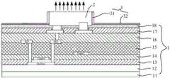
请参阅图1,一种显示面板包括TFT基板1、位于FTF基板1上的Micro-LED 2以及至少包裹所述Micro-LED 2的侧壁的反光层3。在一种实施方式中,所述TFT基板1自下而上依次包括衬底基板11、用于阻挡水汽和杂质的阻挡层12、第一栅极绝缘层13、第二栅极绝缘层14、用于绝缘的介质层15、第一平坦化层16、绝缘层17和第二平坦化层18。所述反光层3至少包裹所述Micro-LED 2的侧壁至少包括如下情况:1)仅包裹所述Micro-LED 2的侧壁,也就是说,只包括如图所示的第一反光层31;2)不仅包裹Micro-LED 2的侧壁,而且,还位于相邻的Micro-LED 2之间,也就是说包括第一反光层31和第二反光层32。在发光层3包括第二反光层32的情况下,第一反光层31和第二反光层32可以通过金属溅射工艺形成,这样,工艺简单,胶体曝光深度等容易控制。在本申请中,因为Micro-LED 2通过引脚处阴极及阳极传输电流后发光,所述反光层3未与Micro-LED 2的任何导电类膜层接触,Micro-LED 2本身具备一层无机层保护层(除引脚外,其余表面均被无机层覆盖),也不会与反光层3产生相互影响。该反光层3使得所述Micro-LED 2发出的光线从所述Micro-LED 2的顶部导出。下面说明该反光层3如何导出Micro-LED 2的光线如下:Referring to FIG. 1 , a display panel includes a
请参阅1并结合图8,因为Micro-LED是点光源,其发射的光线有一部分不会从沿图中箭头所示方向竖直射出,在Micro-LED 2的侧壁被所述反光层3包裹的情况下,Micro-LED2发出的光线会在反光层3上发生反射,如图8示意出光线的传播路径,因此,其发出的光线全部从Micro-LED 2的顶部射出,提高了出光效果,增强了显示效果,特别是在该反光层3配合Micro-LED 2本身的出光面21可以使得Micro-LED 2的全部光线从Micro-LED 2的顶部射出,更加提升了出光效率以及增强了显示效果。此外,该反光层3可以通过BP设备制作,在制作过程中,胶体曝光深度和涂胶均匀性容易控制,因此,这种反光层3的制作难度低。Please refer to 1 in conjunction with Fig. 8, because Micro-LED is a point light source, part of the light emitted by it will not be emitted vertically along the direction shown by the arrow in the figure, and the side wall of Micro-LED 2 is covered by the reflective layer 3 In the case of wrapping, the light emitted by the Micro-LED 2 will be reflected on the reflective layer 3, as shown in Figure 8, which shows the propagation path of the light. Therefore, all the light emitted by the Micro-LED 2 is emitted from the top of the Micro-LED 2, which improves the light output effect. , which enhances the display effect, especially when the reflective layer 3 cooperates with the light-emitting surface 21 of the Micro-LED 2 itself, all the light of the Micro-LED 2 can be emitted from the top of the Micro-LED 2, which further improves the light-emitting efficiency and enhances the display. Effect. In addition, the reflective layer 3 can be manufactured by BP equipment, and during the manufacturing process, the exposure depth of the colloid and the uniformity of glue coating are easily controlled, so the manufacturing difficulty of the reflective layer 3 is low.
在一种实施方式中,为了确保出光效率,所述反光层3和所述Micro-LED 2相对于所述TFT基板1的高度之差小于1微米,也就是说,反光层3的顶面相对于TFT基板1的高度为H1,而Micro-LED 2的顶面相对于TFT基板1的高度为H2,H2-H1<1(单位,微米)。在图1、图6至图8中,反光层3的顶面和所述Micro-LED 2的顶面平齐。In one embodiment, in order to ensure the light extraction efficiency, the difference between the heights of the reflective layer 3 and the Micro-LED 2 relative to the
在本申请中,无论反光层3是否包括第二反光层32,为了防止反光层3与Micro-LED2下方的pad(比如,金属线、金属块等)短路,所述显示面板包括绝缘部件,该绝缘部件位于所述绝缘层17上且至少接触所述Micro-LED 2底部的边缘22。所述至少接触所述Micro-LED2底部的边缘22包括:1)接触底部的边缘22(也就是Micro-LED 2的无机层的下沿),甚至比所述下沿高,但没有位于Micro-LED 2的底面和TFT基板1的绝缘层17;2)既接触Micro-LED2的底部边缘22,还位于其底面和TFT基板1的绝缘层17之间;3)包括前述两种情况,且位于所述绝缘层17的所有部分,比如,还位于绝缘层17上位于相邻的Micro-LED 2之间的部分。针对前述情况,在反光层3包括第一反光层31和第二反光层32的情况下,第二反光层32有如下设置方式:In the present application, no matter whether the reflective layer 3 includes the second
1)针对所述绝缘部件并不位于相邻的Micro-LED 2之间的情况,所述第二反光层32位于所述绝缘层17上,该绝缘部件位于第二反光层32的两端;1) In the case where the insulating member is not located between the
2)针对所述绝缘部件位于相邻的Micro-LED 2之间的情况,所述绝缘部件是形成于所述绝缘层17上的平坦化层(如图1、图3至图8所示,第二平坦化层18),所述第二反光层32位于平坦化层上(第二平坦化层18)。在该种实施方式中,通过BP设备形成该平坦化层(第二平坦化层18),容易控制涂覆量,制造难度低。2) For the case where the insulating member is located between adjacent Micro-LEDs 2, the insulating member is a planarization layer formed on the insulating layer 17 (as shown in FIG. 1, FIG. 3 to FIG. 8, The second planarization layer 18), the second
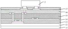
请参阅图7,在一种实施方式中,所述显示面板包括位于相邻的Micro-LED 2之间的所述第二反光层32上的遮光层4(Black Matrix,或者,BM)。通过设置所述遮光层4,可以降低除Micro-LED发光单元外的部分对环境光反射,增强显示效果。Referring to FIG. 7 , in one embodiment, the display panel includes a light-shielding layer 4 (Black Matrix, or BM) located on the second light-reflecting
在另一方面,本申请还公开一种显示装置,该显示装置包括前述任何一种显示面板。这种显示装置比如是智能手机、虚拟显示屏幕、电视等等。In another aspect, the present application also discloses a display device comprising any one of the aforementioned display panels. Such display devices are, for example, smartphones, virtual display screens, televisions, and the like.
请参阅图2至图6,一种显示面板的制造方法包括如下步骤:将Micro-LED置于TFT基板的上方;形成至少包裹所述Micro-LED 2的侧壁的反光层3,该反光层3使得所述Micro-LED 2的出光从所述Micro-LED 2的顶部导出。在一种实施方式中,形成所述反光层前,涂覆平坦化材料形成第二平坦化层,所述第二平坦化层的至少部分位于所述Micro-LED的下方,其实现方式如下:所述TFT基板包括衬底基板11、用于阻挡水汽和杂质的阻挡层12、第一栅极绝缘层13、第二栅极绝缘层14、用于绝缘的介质层15、第一平坦化层16和绝缘层17以及在绝缘层17上涂覆平坦化材料形成的第二平坦化层18,如图3所示。如前所述,在优选实施方式中,确保第二平坦化层18至少位于所述Micro-LED 2底部的边缘和所述TFT基板1的绝缘层17之间(也就是自绝缘层至17少到达Micro-LED 2的无机层的下沿)。所述涂覆量以及其他工艺条件可以根据实际情况处理,只要能形成所述第二平坦化层18即可。所述第二平坦化层18的材料可以是惯用的平坦化材料,包含亚克力体系的JEM-608,聚酰亚胺体系的DL-1000系列;也可以是不具有导电特性的导热硅胶。晶体管及其连接线形成在上述的这些层内。比如,晶体管的有源层可形成在阻挡层12的上方;晶体管的栅极可形成在第一栅极绝缘层13的上方,并被第二栅极绝缘层14所覆盖;晶体管的源漏区可通过设置在第一栅极绝缘层13、第二栅极绝缘层14、介质层15、第一平坦化层16内的金属连接孔与外部(比如,Micro-LED 2的电源供应端)相接。Referring to FIGS. 2 to 6 , a method for manufacturing a display panel includes the following steps: placing a Micro-LED on a TFT substrate; forming a reflective layer 3 surrounding at least the sidewall of the Micro-LED 2 , the reflective layer 3. The light emitted from the
在这种制造方法中,所述反光层3可以只包括所述第一反光层31,也可以既包括所述第一反光层31,也包括第二反光层32。在所述反光层3只包括第一反光层31的情况下,本领域技术人员可以基于光刻和刻蚀的思路形成所述反光层3。由于所述反光层3包括第一反光层31和第二反光层32的情况下,制造工艺简单,详细说明其制造步骤如下:In this manufacturing method, the reflective layer 3 may only include the first
请参阅图4,形成位于所述第二平坦化层18上的所述反光层3,该反光层3包裹所述Micro-LED的侧壁并位于相邻的Micro-LED之间,更为具体的,进行整面反射金属溅射,在所述第二平坦化层18上形成所述反光层3(包括第一反光层31、第二反光层32和位于Micro-LED 2顶部的反光层)。反光层3可以是由材料为Al或Ag构成的单层结构,也可以是叠层结构,比如,Al/ITO、Ag/ITO等叠层结构。在一种实施方式中,为了在确保Micro-LED 2出光率的前提下使得制造成本低,所述反光层3的厚度为500埃~2000埃,比如,500埃、600埃、700埃、800埃、900埃、1000埃、1100埃、1200埃、1300埃、1400埃、1500埃、1600埃、1700埃、1800埃、1900埃或2000埃。Referring to FIG. 4, the reflective layer 3 is formed on the
请参阅图5并结合图4,涂覆光刻胶5(PR),使得光刻胶5填平相邻Micro LED 2之间中的空间,露出Micro LED 2的顶部。Referring to FIG. 5 in conjunction with FIG. 4 , a photoresist 5 (PR) is applied so that the photoresist 5 fills up the space between the
请参阅图6并结合图5,进行反光层3刻蚀,以去掉位于所述Micro-LED 2顶部的反光层以及去除相邻Micro-LED 2之间的光刻胶5,由此,所述反光层3包括第一反光层31和第二反光层32。Referring to FIG. 6 and in conjunction with FIG. 5, the reflective layer 3 is etched to remove the reflective layer on the top of the Micro-LEDs 2 and remove the photoresist 5 between the
请参阅图7,在进一步实施方式中,根据现实环境要求,在去除相邻Micro-LED 2之间的光刻胶5后,可在相邻Micro-LED 2之间进行黑色有机材料(BM)制作,以便形成位于相邻Micro-LED 2之间的反光层上的遮光层4。遮光层4可降低除LED发光单元外的部分对环境光反射,增强显示效果。Referring to FIG. 7 , in a further embodiment, according to actual environmental requirements, after removing the photoresist 5 between the
以上所述仅是本申请的较佳实施方式而已,并非对本申请做任何形式上的限制,虽然本申请已以较佳实施方式揭露如上,然而并非用以限定本申请,任何熟悉本专业的技术人员,在不脱离本申请技术方案的范围内,当可利用上述揭示的技术内容做出些许更动或修饰为等同变化的等效实施方式,但凡是未脱离本申请技术方案的内容,依据本申请的技术实质对以上实施方式所作的任何简单修改、等同变化与修饰,均仍属于本申请技术方案的范围内。The above is only the preferred embodiment of the application, and does not limit the application in any form. Although the application has been disclosed in the preferred embodiment as above, it is not intended to limit the application. Anyone familiar with this professional technology Personnel, without departing from the scope of the technical solution of the present application, can make some changes or modifications to equivalent embodiments of equivalent changes by using the technical content disclosed above, provided that any content that does not depart from the technical solution of the present application, according to this Any simple modifications, equivalent changes and modifications made to the above embodiments by the technical essence of the application still fall within the scope of the technical solutions of the present application.
Claims (10)
Translated fromChinesePriority Applications (3)
| Application Number | Priority Date | Filing Date | Title |
|---|---|---|---|
| CN202010320861.3ACN111477653B (en) | 2020-04-22 | 2020-04-22 | Display panel, display device and manufacturing method of display panel |
| PCT/CN2021/078417WO2021213009A1 (en) | 2020-04-22 | 2021-03-01 | Display panel, display device, and method for manufacturing display panel |
| US17/762,939US20220393075A1 (en) | 2020-04-22 | 2021-03-01 | Display panels, display apparatuses and methods of manufacturing display panels |
Applications Claiming Priority (1)
| Application Number | Priority Date | Filing Date | Title |
|---|---|---|---|
| CN202010320861.3ACN111477653B (en) | 2020-04-22 | 2020-04-22 | Display panel, display device and manufacturing method of display panel |
Publications (2)
| Publication Number | Publication Date |
|---|---|
| CN111477653Atrue CN111477653A (en) | 2020-07-31 |
| CN111477653B CN111477653B (en) | 2023-08-15 |
Family
ID=71755317
Family Applications (1)
| Application Number | Title | Priority Date | Filing Date |
|---|---|---|---|
| CN202010320861.3AActiveCN111477653B (en) | 2020-04-22 | 2020-04-22 | Display panel, display device and manufacturing method of display panel |
Country Status (3)
| Country | Link |
|---|---|
| US (1) | US20220393075A1 (en) |
| CN (1) | CN111477653B (en) |
| WO (1) | WO2021213009A1 (en) |
Cited By (9)
| Publication number | Priority date | Publication date | Assignee | Title |
|---|---|---|---|---|
| CN112382206A (en)* | 2020-11-13 | 2021-02-19 | Tcl华星光电技术有限公司 | Back plate and LED panel |
| CN112540482A (en)* | 2020-12-04 | 2021-03-23 | Tcl华星光电技术有限公司 | Backlight module, backlight module manufacturing method and display panel |
| CN112669720A (en)* | 2021-01-12 | 2021-04-16 | Tcl华星光电技术有限公司 | LED panel and preparation method thereof |
| CN112909145A (en)* | 2021-01-20 | 2021-06-04 | 深圳市华星光电半导体显示技术有限公司 | Display panel and preparation method thereof |
| WO2021213009A1 (en)* | 2020-04-22 | 2021-10-28 | 京东方科技集团股份有限公司 | Display panel, display device, and method for manufacturing display panel |
| CN114122237A (en)* | 2021-11-10 | 2022-03-01 | 惠州华星光电显示有限公司 | Display panel and preparation method thereof |
| JP2023093069A (en)* | 2021-12-22 | 2023-07-04 | 株式会社ジャパンディスプレイ | Display device |
| US11811013B2 (en) | 2021-04-09 | 2023-11-07 | Au Optronics Corporation | Display panel |
| WO2025001673A1 (en)* | 2023-06-30 | 2025-01-02 | 厦门市芯颖显示科技有限公司 | Display panel and preparation method therefor, and display apparatus |
Families Citing this family (1)
| Publication number | Priority date | Publication date | Assignee | Title |
|---|---|---|---|---|
| CN114725273B (en)* | 2022-03-31 | 2025-09-12 | 上海天马微电子有限公司 | Display panel and display device |
Citations (4)
| Publication number | Priority date | Publication date | Assignee | Title |
|---|---|---|---|---|
| US20140367705A1 (en)* | 2013-06-17 | 2014-12-18 | LuxVue Technology Corporation | Reflective bank structure and method for integrating a light emitting device |
| US20170263178A1 (en)* | 2016-03-10 | 2017-09-14 | Samsung Display Co., Ltd. | Display device including light-emitting diodes |
| US20180090058A1 (en)* | 2016-09-23 | 2018-03-29 | Hong Kong Beida Jade Bird Display Limited | Micro Display Panels With Integrated Micro-Reflectors |
| WO2019147589A1 (en)* | 2018-01-24 | 2019-08-01 | Apple Inc. | Micro led based display panel |
Family Cites Families (11)
| Publication number | Priority date | Publication date | Assignee | Title |
|---|---|---|---|---|
| JP4587515B2 (en)* | 2000-02-28 | 2010-11-24 | 京セラ株式会社 | Manufacturing method of semiconductor light emitting device |
| JP2004031669A (en)* | 2002-06-26 | 2004-01-29 | Seiko Epson Corp | Semiconductor element member, semiconductor device, manufacturing method thereof, electro-optical device, and electronic equipment |
| CN100414704C (en)* | 2006-06-30 | 2008-08-27 | 广州南科集成电子有限公司 | Planar flip-chip LED integrated chip and manufacturing method |
| TWI456021B (en)* | 2011-09-30 | 2014-10-11 | 達邁科技股份有限公司 | Polymer film and application of illuminating device |
| DE102015111910A1 (en)* | 2015-07-22 | 2017-01-26 | Osram Opto Semiconductors Gmbh | Optoelectronic component, composite of optoelectronic components and method for producing an optoelectronic component |
| CN107994109A (en)* | 2016-10-27 | 2018-05-04 | 佛山市国星光电股份有限公司 | A kind of COB display modules and its manufacture method |
| US11024773B2 (en)* | 2016-11-07 | 2021-06-01 | Goertek. Inc | Micro-LED with vertical structure, display device, electronics apparatus and manufacturing method |
| KR102136579B1 (en)* | 2018-07-27 | 2020-07-22 | 서울대학교산학협력단 | Display device |
| KR102694329B1 (en)* | 2018-12-10 | 2024-08-13 | 삼성전자주식회사 | Display module, display apparatus including the same and method of manufacturing display module |
| CN110164322A (en)* | 2019-05-22 | 2019-08-23 | 深圳市华星光电半导体显示技术有限公司 | A kind of display panel and electronic device |
| CN111477653B (en)* | 2020-04-22 | 2023-08-15 | 京东方科技集团股份有限公司 | Display panel, display device and manufacturing method of display panel |
- 2020
- 2020-04-22CNCN202010320861.3Apatent/CN111477653B/enactiveActive
- 2021
- 2021-03-01WOPCT/CN2021/078417patent/WO2021213009A1/ennot_activeCeased
- 2021-03-01USUS17/762,939patent/US20220393075A1/ennot_activeAbandoned
Patent Citations (4)
| Publication number | Priority date | Publication date | Assignee | Title |
|---|---|---|---|---|
| US20140367705A1 (en)* | 2013-06-17 | 2014-12-18 | LuxVue Technology Corporation | Reflective bank structure and method for integrating a light emitting device |
| US20170263178A1 (en)* | 2016-03-10 | 2017-09-14 | Samsung Display Co., Ltd. | Display device including light-emitting diodes |
| US20180090058A1 (en)* | 2016-09-23 | 2018-03-29 | Hong Kong Beida Jade Bird Display Limited | Micro Display Panels With Integrated Micro-Reflectors |
| WO2019147589A1 (en)* | 2018-01-24 | 2019-08-01 | Apple Inc. | Micro led based display panel |
Cited By (14)
| Publication number | Priority date | Publication date | Assignee | Title |
|---|---|---|---|---|
| WO2021213009A1 (en)* | 2020-04-22 | 2021-10-28 | 京东方科技集团股份有限公司 | Display panel, display device, and method for manufacturing display panel |
| CN112382206B (en)* | 2020-11-13 | 2022-07-12 | Tcl华星光电技术有限公司 | Backplane and LED Panel |
| CN112382206A (en)* | 2020-11-13 | 2021-02-19 | Tcl华星光电技术有限公司 | Back plate and LED panel |
| US12107200B2 (en) | 2020-11-13 | 2024-10-01 | Tcl China Star Optoelectronics Technology Co., Ltd. | Backplane and light emitting diode panel |
| WO2022099862A1 (en)* | 2020-11-13 | 2022-05-19 | Tcl华星光电技术有限公司 | Backplane and led panel |
| CN112540482A (en)* | 2020-12-04 | 2021-03-23 | Tcl华星光电技术有限公司 | Backlight module, backlight module manufacturing method and display panel |
| CN112669720A (en)* | 2021-01-12 | 2021-04-16 | Tcl华星光电技术有限公司 | LED panel and preparation method thereof |
| CN112669720B (en)* | 2021-01-12 | 2022-06-10 | Tcl华星光电技术有限公司 | LED panel and preparation method thereof |
| CN112909145A (en)* | 2021-01-20 | 2021-06-04 | 深圳市华星光电半导体显示技术有限公司 | Display panel and preparation method thereof |
| US11811013B2 (en) | 2021-04-09 | 2023-11-07 | Au Optronics Corporation | Display panel |
| CN114122237A (en)* | 2021-11-10 | 2022-03-01 | 惠州华星光电显示有限公司 | Display panel and preparation method thereof |
| JP2023093069A (en)* | 2021-12-22 | 2023-07-04 | 株式会社ジャパンディスプレイ | Display device |
| JP7749448B2 (en) | 2021-12-22 | 2025-10-06 | 株式会社ジャパンディスプレイ | display device |
| WO2025001673A1 (en)* | 2023-06-30 | 2025-01-02 | 厦门市芯颖显示科技有限公司 | Display panel and preparation method therefor, and display apparatus |
Also Published As
| Publication number | Publication date |
|---|---|
| WO2021213009A1 (en) | 2021-10-28 |
| US20220393075A1 (en) | 2022-12-08 |
| CN111477653B (en) | 2023-08-15 |
Similar Documents
| Publication | Publication Date | Title |
|---|---|---|
| CN111477653B (en) | Display panel, display device and manufacturing method of display panel | |
| CN102194980B (en) | Light emitting diode package and lighting system including the same | |
| CN111710691B (en) | Flexible Micro-LED display panel and manufacturing method thereof | |
| CN102194949B (en) | Light emitting device | |
| CN109037476A (en) | A kind of display base plate and preparation method thereof, display device | |
| CN109065590B (en) | Organic light-emitting display substrate and method of making the same, and organic light-emitting display device | |
| CN109411583B (en) | Light-emitting unit, method for manufacturing the same, and display device | |
| CN107579166A (en) | Display panel, display device, and display panel manufacturing method | |
| CN111370446A (en) | OLED display panel and OLED display device | |
| US20190304958A1 (en) | Micro led display panel and manufacturing method thereof | |
| CN102738355A (en) | Package with light emitting element and manufacturing method thereof | |
| CN104103673A (en) | Organic light emitting diode (OLED) displayer and preparation method thereof | |
| CN204391161U (en) | Pixel structure and display device | |
| CN107422555A (en) | A kind of display device, array base palte and preparation method thereof | |
| US20170160569A1 (en) | Array substrate having conductive planar layer and method of manufacturing the same | |
| WO2019205438A1 (en) | Drive substrate, preparation method and micro led array light-emitting backlight module | |
| JP2015088418A (en) | Organic el element, and image display apparatus and illumination apparatus including the same | |
| CN111106153B (en) | Display panel, manufacturing method thereof and display device | |
| CN115101545A (en) | Display panel and driving substrate thereof | |
| CN115513225B (en) | Display substrate, method for preparing display substrate, and display device | |
| WO2015119203A1 (en) | Front plate for el element and illumination device | |
| CN115915821A (en) | Display panel, manufacturing method and display device | |
| KR102868030B1 (en) | Light emitting display apparatus | |
| TWI797915B (en) | Mirror display | |
| CN114864773B (en) | Light emitting diode display device and manufacturing method thereof |
Legal Events
| Date | Code | Title | Description |
|---|---|---|---|
| PB01 | Publication | ||
| PB01 | Publication | ||
| SE01 | Entry into force of request for substantive examination | ||
| SE01 | Entry into force of request for substantive examination | ||
| GR01 | Patent grant | ||
| GR01 | Patent grant |