CN111477625A - A kind of semi-floating gate memory based on defect trapping material and preparation method thereof - Google Patents
A kind of semi-floating gate memory based on defect trapping material and preparation method thereofDownload PDFInfo
- Publication number
- CN111477625A CN111477625ACN202010346220.5ACN202010346220ACN111477625ACN 111477625 ACN111477625 ACN 111477625ACN 202010346220 ACN202010346220 ACN 202010346220ACN 111477625 ACN111477625 ACN 111477625A
- Authority
- CN
- China
- Prior art keywords
- gate
- semi
- floating gate
- dielectric layer
- well region
- Prior art date
- Legal status (The legal status is an assumption and is not a legal conclusion. Google has not performed a legal analysis and makes no representation as to the accuracy of the status listed.)
- Granted
Links
Images


Classifications
- H—ELECTRICITY
- H10—SEMICONDUCTOR DEVICES; ELECTRIC SOLID-STATE DEVICES NOT OTHERWISE PROVIDED FOR
- H10B—ELECTRONIC MEMORY DEVICES
- H10B12/00—Dynamic random access memory [DRAM] devices
- H10B12/20—DRAM devices comprising floating-body transistors, e.g. floating-body cells
- H—ELECTRICITY
- H10—SEMICONDUCTOR DEVICES; ELECTRIC SOLID-STATE DEVICES NOT OTHERWISE PROVIDED FOR
- H10B—ELECTRONIC MEMORY DEVICES
- H10B12/00—Dynamic random access memory [DRAM] devices
- H10B12/01—Manufacture or treatment
Landscapes
- Engineering & Computer Science (AREA)
- Manufacturing & Machinery (AREA)
- Non-Volatile Memory (AREA)
- Semiconductor Memories (AREA)
Abstract
Translated fromChinese
Description
Translated fromChinese技术领域technical field
本发明属于半导体存储器技术领域,具体涉及一种基于缺陷俘获材料的半浮栅存储器及其制备方法。The invention belongs to the technical field of semiconductor memory, and in particular relates to a semi-floating gate memory based on defect trapping materials and a preparation method thereof.
背景技术Background technique
目前,集成电路芯片中使用的DRAM器件主要为1T1C结构,即一个晶体管串联一个电容器,通过晶体管的开关实现对电容器的充电和放电,从而实现DRAM器件0和1之间的转换。随着器件尺寸越来越小,集成电路芯片中使用的DRAM器件正面临越来越多的问题,比如DRAM器件要求64ms刷新一次,因此电容器的电容值必须保持在一定数值以上以保证有足够长的电荷保持时间,但是随着集成电路特征尺寸的缩小,大电容的制造已经越来越困难,而且已经占了制造成本的30%以上。半浮栅存储器是DRAM器件的替代概念,不同于通常的1T1C结构,半浮栅器件由一个浮栅晶体管和嵌入式隧穿晶体管组成,通过嵌入式隧穿晶体管的沟道对浮栅晶体管的浮栅进行写入和擦除操作。从半浮栅存储器的工作原理我们可以看出,半浮栅存储器的电荷保持能力由半浮栅的材料决定。因此,如何进一步改进半浮栅的材料成为进一步提高半浮栅存储器的电荷保持能力,增加电荷保持时间的关键。此外,伴随着多晶硅浮栅尺寸的缩小,通过栅间介质的冲击电流过大,会给存储器带来可靠性问题。而且,多晶硅浮栅存在多晶硅耗尽效应,要生长光滑、足够薄的多晶硅薄膜的工艺相对复杂。At present, DRAM devices used in integrated circuit chips are mainly 1T1C structures, that is, a transistor is connected in series with a capacitor, and the capacitor is charged and discharged through the switch of the transistor, thereby realizing the conversion between DRAM devices 0 and 1. As the device size becomes smaller and smaller, DRAM devices used in integrated circuit chips are facing more and more problems. For example, DRAM devices require 64ms to refresh once, so the capacitance value of the capacitor must be kept above a certain value to ensure a sufficient length of time. However, as the feature size of integrated circuits shrinks, the manufacture of large capacitors has become more and more difficult, and has accounted for more than 30% of the manufacturing cost. Semi-floating-gate memory is an alternative concept to DRAM devices. Different from the usual 1T1C structure, a semi-floating-gate device consists of a floating-gate transistor and an embedded tunneling transistor. The floating-gate transistor is floated through the channel of the embedded tunneling transistor. gate for write and erase operations. From the working principle of the semi-floating gate memory, we can see that the charge retention capability of the semi-floating gate memory is determined by the material of the semi-floating gate. Therefore, how to further improve the material of the semi-floating gate becomes the key to further improve the charge retention capability of the semi-floating gate memory and increase the charge retention time. In addition, with the shrinking of the size of the polysilicon floating gate, the inrush current through the inter-gate dielectric is too large, which will bring reliability problems to the memory. Moreover, the polysilicon floating gate has a polysilicon depletion effect, and the process for growing a smooth and sufficiently thin polysilicon film is relatively complicated.
发明内容SUMMARY OF THE INVENTION
本发明的目的在于提供一种能够增强电荷保持能力、增加存储器刷新时间的基于缺陷俘获材料的半浮栅存储器及其制备方法。The purpose of the present invention is to provide a semi-floating gate memory based on defect trapping materials capable of enhancing the charge retention capability and increasing the refresh time of the memory and a preparation method thereof.
本发明提供的基于缺陷俘获材料的半浮栅存储器,包括:The semi-floating gate memory based on defect trapping material provided by the present invention includes:
半导体衬底,其为第一掺杂类型;a semiconductor substrate of the first doping type;
半浮栅阱区,其为第二掺杂类型,形成于所述半导体衬底表面;a semi-floating gate well region, which is of the second doping type, formed on the surface of the semiconductor substrate;
U型槽,贯穿所述半浮栅阱区,其底部处于所述半浮栅阱区的下边界;The U-shaped groove runs through the semi-floating gate well region, and its bottom is at the lower boundary of the semi-floating gate well region;
第一栅极叠层,包括第一栅介质层、第一金属栅和浮栅,其中第一栅介质层覆盖所述U型槽的表面,并在所述半浮栅阱区形成开口;所述第一金属栅覆盖所述第一栅介质层并在所述开口处与所述半浮栅阱区接触;所述浮栅覆盖所述第一金属栅;The first gate stack includes a first gate dielectric layer, a first metal gate and a floating gate, wherein the first gate dielectric layer covers the surface of the U-shaped groove and forms an opening in the semi-floating gate well region; the first metal gate covers the first gate dielectric layer and is in contact with the semi-floating gate well region at the opening; the floating gate covers the first metal gate;
第二栅极叠层,包括第二栅介质层和第二金属栅,所述第二栅介质层覆盖所述浮栅表面和部分所述半浮栅阱区表面,所述第二金属栅覆盖所述第二栅介质层;栅极侧墙,位于所述第一栅极叠层和所述第二栅极叠层两侧;The second gate stack includes a second gate dielectric layer and a second metal gate, the second gate dielectric layer covers the surface of the floating gate and part of the surface of the semi-floating gate well region, and the second metal gate covers the second gate dielectric layer; gate spacers located on both sides of the first gate stack and the second gate stack;
源极和漏极,形成于所述半浮栅阱区中,位于所述第一栅极叠层和所述第二栅极叠层两侧;a source electrode and a drain electrode, formed in the semi-floating gate well region, on both sides of the first gate stack and the second gate stack;
其中,所述浮栅为缺陷俘获材料。Wherein, the floating gate is a defect trapping material.
本发明的基于缺陷俘获材料的半浮栅存储器中,优选为,所述第一金属栅的厚度为3~5nm。In the semi-floating gate memory based on the defect trapping material of the present invention, preferably, the thickness of the first metal gate is 3-5 nm.
本发明的基于缺陷俘获材料的半浮栅存储器中,优选为,所述缺陷俘获材料为富含深能级缺陷的绝缘材料。In the semi-floating gate memory based on the defect trapping material of the present invention, preferably, the defect trapping material is an insulating material rich in deep level defects.
本发明的基于缺陷俘获材料的半浮栅存储器中,优选为,所述绝缘材料为Si3N4或者SiON。In the semi-floating gate memory based on the defect trapping material of the present invention, preferably, the insulating material is Si3 N4 or SiON.
本发明的基于缺陷俘获材料的半浮栅存储器中,优选为,所述第一栅介质层或所述第二栅介质层为SiO2、Al2O3、ZrO2、HfZrO、HfO2、HfAlO、HfSiO及其任意组合的一种,所述第一金属栅或所述第二金属栅为TiN、TaN、MoN或者WN。In the semi-floating gate memory based on the defect trapping material of the present invention, preferably, the first gate dielectric layer or thesecond gate dielectric layer isSiO2 , Al2O3, ZrO2, HfZrO,HfO2 , HfAlO, HfSiO and any combination thereof, the first metal gate or the second metal gate is TiN, TaN, MoN or WN.
本发明还公开一种基于缺陷俘获材料的半浮栅存储器的制备方法,包括以下步骤:The present invention also discloses a method for preparing a semi-floating gate memory based on the defect trapping material, comprising the following steps:
(1)提供具有第一掺杂类型的半导体衬底,在所述半导体衬底上形成氧化物层;(1) providing a semiconductor substrate having a first doping type, on which an oxide layer is formed;
(2)通过离子注入方式在所述半导体衬底表层区域形成具有第二掺杂类型的半浮栅阱区;(2) forming a semi-floating gate well region with a second doping type in the surface region of the semiconductor substrate by ion implantation;
(3)形成U型槽,使U型槽贯穿所述半浮栅阱区,且其底部处于半所述浮栅阱区的下边界,并去除所述氧化物层;(3) forming a U-shaped groove, so that the U-shaped groove penetrates the half-floating gate well region, and the bottom of the U-shaped groove is located at the lower boundary of the half-floating gate well region, and the oxide layer is removed;
(4)形成第一栅极叠层,依次形成第一栅介质层、第一金属栅和浮栅,使所述第一栅介质层覆盖所述U型槽的表面,并在所述半浮栅阱区形成开口;所述第一金属栅覆盖所述第一栅介质层并在所述开口处与所述半浮栅阱区接触;所述浮栅覆盖所述第一金属栅,其中,所述浮栅为缺陷俘获材料;(4) forming a first gate stack, forming a first gate dielectric layer, a first metal gate and a floating gate in sequence, so that the first gate dielectric layer covers the surface of the U-shaped groove, and the semi-floating gate is formed in the semi-floating gate. an opening is formed in the gate well region; the first metal gate covers the first gate dielectric layer and is in contact with the semi-floating gate well region at the opening; the floating gate covers the first metal gate, wherein, the floating gate is a defect trapping material;
(5)形成第二栅极叠层,依次形成第二栅介质层和第二金属栅,使所述第二栅介质层覆盖所述浮栅表面和部分所述半浮栅阱区表面,所述第二金属栅覆盖所述第二栅介质层;(5) forming a second gate stack, forming a second gate dielectric layer and a second metal gate in sequence, so that the second gate dielectric layer covers the surface of the floating gate and part of the surface of the semi-floating gate well region, so the second metal gate covers the second gate dielectric layer;
(6)在所述第一栅极叠层和所述第二栅极叠层两侧形成栅极侧墙;(6) forming gate spacers on both sides of the first gate stack and the second gate stack;
(7)在所述半浮栅阱区中,所述第一栅极叠层和所述第二栅极叠层两侧形成源极和漏极。(7) In the semi-floating gate well region, a source electrode and a drain electrode are formed on both sides of the first gate stack and the second gate stack.
本发明的基于缺陷俘获材料的半浮栅存储器的制备方法中,优选为,所述第一金属栅的厚度为3~5nm。In the method for preparing the semi-floating gate memory based on the defect trapping material of the present invention, preferably, the thickness of the first metal gate is 3-5 nm.
本发明的基于缺陷俘获材料的半浮栅存储器的制备方法中,优选为,所述缺陷俘获材料为富含深能级缺陷的绝缘材料。In the method for preparing a semi-floating gate memory based on a defect trapping material of the present invention, preferably, the defect trapping material is an insulating material rich in deep level defects.
本发明的基于缺陷俘获材料的半浮栅存储器的制备方法中,优选为,所述绝缘材料为Si3N4或者SiON。In the method for preparing the semi-floating gate memory based on the defect trapping material of the present invention, preferably, the insulating material is Si3 N4 or SiON.
本发明的基于缺陷俘获材料的半浮栅存储器的制备方法中,优选为,所述第一栅介质层或所述第二栅介质层为SiO2、Al2O3、ZrO2、HfZrO、HfO2、HfAlO、HfSiO及其任意组合的一种,所述第一金属栅或所述第二金属栅为TiN、TaN、MoN或者WN。In the preparation method of the semi-floating gate memory based on the defect trapping material of the present invention, preferably, the first gate dielectric layer or the second gate dielectric layer is SiO2 , Al2 O3 , ZrO2 , HfZrO, HfO2. One of HfAlO, HfSiO and any combination thereof, wherein the first metal gate or the second metal gate is TiN, TaN, MoN or WN.
本发明的基于缺陷俘获材料的半浮栅存储器,利用缺陷俘获材料如拥有大量缺陷的绝缘材料取代多晶硅作为浮栅,同时,由于缺陷俘获材料中的缺陷是不连续的,因此通过嵌入一层超薄金属来收集电荷,然后电荷再被缺陷俘获材料中的缺陷所俘获。由于传统的多晶硅材料是连续的,所以如果有一处出现泄漏,那么存储在多晶硅材料的电荷都可以通过该泄漏点进入沟道。相比之下,缺陷俘获材料中的缺陷是不连续的,所以即使出现一处泄漏,其它位置的电荷依然可以固定在缺陷中。也就是说,采用缺陷俘获材料作为浮栅材料可以有效地增强电荷保持能力,从而增加存储器的刷新时间。In the semi-floating gate memory based on the defect trapping material of the present invention, a defect trapping material such as an insulating material with a large number of defects is used to replace polysilicon as the floating gate. The thin metal collects the charge, which is then captured by defects in the defect-trapping material. Since the traditional polysilicon material is continuous, if there is a leakage at one point, the charge stored in the polysilicon material can enter the channel through the leakage point. In contrast, defects in defect-trapping materials are discontinuous, so even if a leak occurs at one location, charges at other locations can remain trapped in the defect. That is to say, the use of defect trapping material as the floating gate material can effectively enhance the charge retention capability, thereby increasing the refresh time of the memory.
附图说明Description of drawings
图1是基于缺陷俘获材料的半浮栅存储器制备方法的流程图。FIG. 1 is a flow chart of a method for fabricating a semi-floating gate memory based on defect trapping materials.
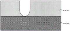
图2是形成氧化物层后的器件结构示意图。FIG. 2 is a schematic diagram of the device structure after the oxide layer is formed.
图3是形成半浮栅阱区后的器件结构示意图。FIG. 3 is a schematic diagram of the structure of the device after the semi-floating gate well region is formed.
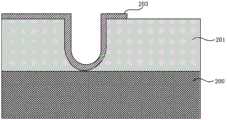
图4是形成U型槽后的器件结构示意图。FIG. 4 is a schematic diagram of the structure of the device after the U-shaped groove is formed.
图5是去除氧化物层后的器件结构示意图。FIG. 5 is a schematic diagram of the device structure after removing the oxide layer.
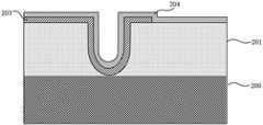
图6~图10是形成第一栅极叠层的各步骤的器件结构示意图。6 to 10 are schematic diagrams of device structures in each step of forming the first gate stack.
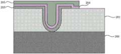
图11~图13是形成第二栅极叠层的各步骤的器件结构示意图。11 to 13 are schematic diagrams of device structures in each step of forming the second gate stack.
图14是形成栅极侧墙后的器件结构示意图。FIG. 14 is a schematic diagram of the device structure after the gate spacers are formed.
图15是形成源极和漏极后的器件结构示意图。FIG. 15 is a schematic diagram of the device structure after the source and drain electrodes are formed.
具体实施方式Detailed ways
下面结合实施例和附图,对本发明作进一步介绍。应当理解,所述实施例仅用以解释本发明,并不用于限定本发明。本领域普通技术人员在没有做出创造性劳动前提下所获得的所有其它实施例,都属于本发明保护的范围。The present invention will be further introduced below in conjunction with the embodiments and the accompanying drawings. It should be understood that the embodiments are only used to explain the present invention, and are not intended to limit the present invention. All other embodiments obtained by persons of ordinary skill in the art without creative efforts shall fall within the protection scope of the present invention.
在本发明的描述中,需要说明的是,术语“上”、“下”、“垂直”“水平”等指示的方位或位置关系为基于附图所示的方位或位置关系,仅是为了便于描述本发明和简化描述,而不是指示或暗示所指的装置或元件必须具有特定的方位、以特定的方位构造和操作,因此不能理解为对本发明的限制。此外,术语“第一”、“第二”仅用于描述目的,而不能理解为指示或暗示相对重要性。In the description of the present invention, it should be noted that the orientation or positional relationship indicated by the terms "upper", "lower", "vertical", "horizontal", etc. is based on the orientation or positional relationship shown in the accompanying drawings, and is only for convenience The invention is described and simplified without indicating or implying that the device or element referred to must have a particular orientation, be constructed and operate in a particular orientation, and therefore should not be construed as limiting the invention. Furthermore, the terms "first" and "second" are used for descriptive purposes only and should not be construed to indicate or imply relative importance.
此外,在下文中描述了本发明的许多特定的细节,例如器件的结构、材料、尺寸、处理工艺和技术,以便更清楚地理解本发明。但正如本领域的技术人员能够理解的那样,可以不按照这些特定的细节来实现本发明。除非在下文中特别指出,器件中的各个部分可以由本领域的技术人员公知的材料构成,或者可以采用将来开发的具有类似功能的材料。Furthermore, numerous specific details of the present invention are described below, such as device structures, materials, dimensions, processing techniques and techniques, in order to provide a clearer understanding of the present invention. However, as can be understood by one skilled in the art, the present invention may be practiced without these specific details. Unless specifically indicated below, various parts of the device may be constructed of materials known to those skilled in the art, or materials developed in the future with similar functions may be employed.
图1是基于缺陷俘获材料的半浮栅存储器的制备方法的流程图,图2~15示出了基于缺陷俘获材料的半浮栅存储器的制备方法各步骤的结构示意图。如图1所示,具体制备步骤为:FIG. 1 is a flow chart of a method for fabricating a semi-floating gate memory based on a defect trapping material, and FIGS. 2 to 15 show structural schematic diagrams of each step of the method for fabricating a semi-floating gate memory based on a defect trapping material. As shown in Figure 1, the specific preparation steps are:
步骤S1,提供具有第一掺杂类型的半导体衬底200。然后,在半导体衬底200表面生长一层氧化物202,该氧化物通常是SiO2,主要是为了避免半导体衬底本身直接遭受离子轰击而产生缺陷,所得结构如图2所示。半导体衬底200可以是各种形式的合适衬底,例如半导体衬底如Si、Ge等及化合物半导体衬底如SiGe、GaAs、GaSb、AlAs、InAs、InP、GaN、SiC、InGaAs、InSb、InGaSb等,绝缘体上半导体衬底(SOI)等。为方便说明,以下以Si衬底为例进行描述。步骤S2,形成具有第二掺杂类型的半浮栅阱区201。通过离子注入方式在半导体衬底200表层区域形成具有第二掺杂类型的半浮栅阱区201,所得结构如图3所示。在本实施方式中,第一掺杂类型为p型,第二掺杂类型为n型,也即半导体衬底200为p型掺杂的衬底,在其表面区域形成n型轻掺杂的半浮栅阱区201。In step S1, a
步骤S3,形成U型槽。具体而言,旋涂光刻胶,并通过曝光和显影等光刻工艺定义U型槽的位置。通过干法蚀刻,如离子铣蚀刻、等离子蚀刻、反应离子蚀刻、激光烧蚀,或者通过使用蚀刻剂溶液的湿法蚀刻进行图案化,从而在半浮栅阱区201中形成U型槽。使U型槽贯穿半浮栅阱区201,也即U型槽的底部处于半浮栅阱区201的下边界,所得结构如图4所示。接着,采用前述相同的光刻和刻蚀的方法去除氧化物202,所得结构如图5所示。Step S3, forming a U-shaped groove. Specifically, the photoresist is spin-coated, and the position of the U-shaped groove is defined by photolithography processes such as exposure and development. U-shaped grooves are formed in the semi-floating
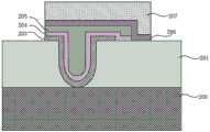
步骤S4,形成第一栅极叠层,包括形成第一栅介质层、第一金属栅和浮栅。具体而言,包括以下步骤,结合图6~图10进行说明。在上述器件结构上采用原子层沉积方法淀积HfO2层作为第一栅介质层203,使其覆盖U型槽表面及半浮栅阱区201表面,所得结构如图6所示。之后旋涂光刻胶,并通过曝光和显影等光刻工艺定义隧穿晶体管的源端起始位置。通过干法蚀刻,如离子铣蚀刻、等离子蚀刻、反应离子蚀刻、激光烧蚀,或者通过使用蚀刻剂溶液的湿法蚀刻进行图案化,去除部分HfO2层203,使部分半浮栅阱区201表面暴露,所得结构如图7所示。然后,利用原子层沉积方法形成厚度介于3~5nm之间的TiN层作为第一金属栅204,所得结构如图8所示。紧接着采用化学气相沉积方法形成缺陷俘获材料Si3N4层作为浮栅205,所得结构如图9所示。最后,在浮栅205上旋涂光刻胶,并通过其中包括曝光和显影的光刻工艺将光刻胶形成用于限定第一栅极叠层形状的图案。通过干法蚀刻,如离子铣蚀刻、等离子蚀刻、反应离子蚀刻、激光烧蚀,或者通过使用蚀刻剂溶液的湿法蚀刻,去除部分TiN层204和部分Si3N4层205,所得结构如图10所示。然后,通过在溶剂中溶解或灰化去除光刻胶。在本实施方式中选用HfO2作为第一栅介质层,选用TiN作为第一金属栅,选用缺陷俘获材料Si3N4作为浮栅。但是本发明不限定于此,第一栅介质层可以是选自SiO2、Al2O3、ZrO2、HfZrO、HfO2、HfAlO、HfSiO及其任意组合的一种。第一金属栅例如可以是选自TiN、TaN、MoN或者WN的一种。缺陷俘获材料可以选自富含深能级缺陷的绝缘材料,例如Si3N4或者SiON。由于传统的多晶硅材料是连续的,所以如果有一处出现泄漏,那么存储在多晶硅材料的电荷都可以通过该泄漏点进入沟道。相比之下,缺陷俘获材料中的缺陷是不连续的,所以即使出现一处泄漏,其它位置的电荷依然可以固定在缺陷中。也就是说,采用缺陷俘获材料作为浮栅可以有效地增强电荷保持能力,从而增加存储器的刷新时间。此外,通过嵌入一层超薄金属即第一金属栅,利于收集电荷,然后电荷再被绝缘材料中的缺陷所俘获。Step S4, forming a first gate stack, including forming a first gate dielectric layer, a first metal gate and a floating gate. Specifically, it includes the following steps, which will be described with reference to FIGS. 6 to 10 . Atomic layer deposition is used to deposit aHfO2 layer on the above device structure as the first
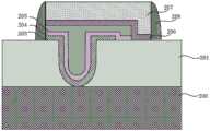
步骤S5,形成第二栅极叠层,包括形成第二栅介质层和第二金属栅。具体而言,包括以下步骤,结合图11~图13进行说明。在上述器件结构上采用原子层沉积方法淀积HfO2层作为第二栅介质层206,所得结构如图11所示。然后利用原子层沉积方法形成TiN层作为第二金属栅207,所得结构如图12所示。最后在第二金属栅207上旋涂光刻胶,并通过其中包括曝光和显影的光刻工艺将光刻胶形成用于限定第二栅极叠层的形状的图案。通过干法蚀刻,如离子铣蚀刻、等离子蚀刻、反应离子蚀刻、激光烧蚀,或者通过使用蚀刻剂溶液的湿法蚀刻,去除一侧部分第一栅介质层206和第二金属栅207,以及去除另一侧部分第一栅介质层203、第一金属栅204、浮栅205、第二栅介质层206和第二金属栅207,所得结构如图13所示。然后,通过在溶剂中溶解或灰化去除光刻胶。在本实施方式中选用HfO2作为第二栅介质层,选用TiN作为第二金属栅。但是本发明不限定于此,第二栅介质层可以是选自SiO2、Al2O3、ZrO2、HfZrO、HfO2、HfAlO、HfSiO及其任意组合的一种。第二金属栅层例如可以是选自TiN、TaN、MoN或者WN的一种。Step S5, forming a second gate stack, including forming a second gate dielectric layer and a second metal gate. Specifically, it includes the following steps, which will be described with reference to FIGS. 11 to 13 . On the above device structure, an atomic layer deposition method is used to deposit a HfO2 layer as the second
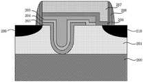
步骤S6,形成栅极侧墙。采用化学气相沉积的方法在半浮栅阱区、第一栅极叠层和第二栅极叠层表面生长SiO2层,然后通过光刻和干法刻蚀的方法去除部分SiO2层,从而在第一栅极叠层和第二栅极叠层两侧形成栅极侧墙208,所得结构如图14所示。当然本发明也可以通过其它淀积工艺形成栅极侧墙,如电子束蒸发、原子层沉积、溅射等,栅极侧墙材料例如也可以是氮化硅等绝缘材料。Step S6, forming gate spacers. A SiO2 layer is grown on the surface of the semi-floating gate well region, the first gate stack and the second gate stack by chemical vapor deposition, and then part of the SiO2 layer is removed by photolithography and dry etching, thereby
步骤S7,形成源极和漏极。旋涂光刻胶,进行光刻工艺限定源极、漏极形状。采用物理气相沉积的方法沉积金属Ni,然后去除光刻胶,最后采用激光退火的方法形成NiSi化合物作为源极209和漏极210,所得结构如图15所示。在本实施方式中选用NiSi作为源漏电极。但是本发明不限定于此,源漏电极可以是选自NiSi、CoSi、TiSi、PtSi、NiPtSi中的一种。采用金属硅化物作为源漏电极,可以显著降低源漏极接触电阻,从而降低功耗。Step S7, forming a source electrode and a drain electrode. The photoresist is spin-coated, and the photolithography process is performed to define the shapes of the source and drain electrodes. Metal Ni is deposited by physical vapor deposition, then the photoresist is removed, and finally, a NiSi compound is formed as the
以上,针对本发明的基于缺陷俘获材料的半浮栅存储器制备方法的具体实施方式进行了详细说明,但是本发明不限定于此。各步骤的具体实施方式根据情况可以不同。此外,部分步骤的顺序可以调换,部分步骤可以省略等。The specific embodiments of the method for fabricating the semi-floating gate memory based on the defect trapping material of the present invention have been described in detail above, but the present invention is not limited thereto. The specific implementation of each step may vary according to the situation. In addition, the order of some steps may be reversed, some steps may be omitted, and the like.
图15是本发明的基于缺陷俘获材料的半浮栅存储器的结构示意图。如图15所示,该基于缺陷俘获材料的半浮栅存储器包括:半导体衬底200,其具有第一掺杂类型。具有U型槽的半浮栅阱区201,其具有第二掺杂类型,位于半导体衬底200表层区域,而且U型槽贯穿半浮栅阱区201,其底部处于半浮栅阱区201的下边界。第一栅极叠层,包括第一栅介质层203、第一金属栅204和浮栅205,其中第一栅介质层203覆盖U型槽的表面,并在半浮栅阱区201形成开口;第一金属栅204覆盖第一栅介质层203并在开口处与半浮栅阱区201接触;浮栅205覆盖第一金属栅204。第二栅极叠层,包括第二栅介质层206和第二金属栅207,第二栅介质层206覆盖浮栅205表面和部分半浮栅阱区201表面,第二金属栅207覆盖第二栅介质层206;栅极侧墙208,位于第一栅极叠层和第二栅极叠层两侧;源极209和漏极210,形成于半浮栅阱区201中,位于第一栅极叠层、第二栅极叠层两侧。其中,浮栅205为缺陷俘获材料。进一步优选地,缺陷俘获材料为富含深能级缺陷的绝缘材料,如Si3N4或者SiON。由于缺陷俘获材料中的缺陷是不连续的,所以即使出现一处泄漏,其它位置的电荷依然可以固定在缺陷中。也就是说,采用缺陷俘获材料作为浮栅可以有效地增强电荷保持能力,从而增加存储器的刷新时间。此外,通过嵌入一层超薄金属即第一金属栅,利于收集电荷,且不会显著增加浮栅材料的整体厚度,金属和缺陷绝缘材料都没有耗尽效应。FIG. 15 is a schematic structural diagram of a semi-floating gate memory based on defect trapping materials of the present invention. As shown in FIG. 15 , the defect trapping material-based semi-floating gate memory includes: a
进一步优选地,半导体衬底可以是各种形式的合适衬底,例如半导体衬底如Si、Ge等及化合物半导体衬底如SiGe、GaAs、GaSb、AlAs、InAs、InP、GaN、SiC、InGaAs、InSb、InGaSb等,绝缘体上半导体衬底(SOI)等。第一栅介质层为SiO2、Al2O3、ZrO2、HfZrO、HfO2、HfAlO、HfSiO及其任意组合的一种。优选地,第一金属栅为TiN、TaN、MoN或者WN,厚度为3~5nm。第二栅介质层为SiO2、Al2O3、ZrO2、HfZrO、HfO2、HfAlO、HfSiO及其任意组合的一种。优选地,第二金属栅为TiN、TaN、MoN或者WN。源、漏电极可以是选自NiSi、CoSi、TiSi、PtSi、NiPtSi中的一种。采用金属硅化物作为源漏电极,可以显著降低源漏极接触电阻,从而降低功耗。Further preferably, the semiconductor substrate may be a suitable substrate in various forms, such as semiconductor substrates such as Si, Ge, etc. and compound semiconductor substrates such as SiGe, GaAs, GaSb, AlAs, InAs, InP, GaN, SiC, InGaAs, InSb, InGaSb, etc., semiconductor-on-insulator substrate (SOI), etc. The first gate dielectric layer is one of SiO2 , Al2 O3 , ZrO2 , HfZrO, HfO2 , HfAlO, HfSiO and any combination thereof. Preferably, the first metal gate is TiN, TaN, MoN or WN, and the thickness is 3-5 nm. The second gate dielectric layer is one of SiO2 , Al2 O3 , ZrO2 , HfZrO, HfO2 , HfAlO, HfSiO and any combination thereof. Preferably, the second metal gate is TiN, TaN, MoN or WN. The source and drain electrodes may be one selected from NiSi, CoSi, TiSi, PtSi, and NiPtSi. Using metal silicide as the source-drain electrode can significantly reduce the source-drain contact resistance, thereby reducing power consumption.
以上所述,仅为本发明的具体实施方式,但本发明的保护范围并不局限于此,任何熟悉本技术领域的技术人员在本发明揭露的技术范围内,可轻易想到的变化或替换,都应涵盖在本发明的保护范围之内。The above are only specific embodiments of the present invention, but the protection scope of the present invention is not limited thereto. Any person skilled in the art who is familiar with the technical scope disclosed by the present invention can easily think of changes or substitutions. All should be included within the protection scope of the present invention.
Claims (10)
Translated fromChinesePriority Applications (1)
| Application Number | Priority Date | Filing Date | Title |
|---|---|---|---|
| CN202010346220.5ACN111477625B (en) | 2020-04-27 | 2020-04-27 | A semi-floating gate memory based on defect-trapping material and its preparation method |
Applications Claiming Priority (1)
| Application Number | Priority Date | Filing Date | Title |
|---|---|---|---|
| CN202010346220.5ACN111477625B (en) | 2020-04-27 | 2020-04-27 | A semi-floating gate memory based on defect-trapping material and its preparation method |
Publications (2)
| Publication Number | Publication Date |
|---|---|
| CN111477625Atrue CN111477625A (en) | 2020-07-31 |
| CN111477625B CN111477625B (en) | 2023-02-07 |
Family
ID=71761842
Family Applications (1)
| Application Number | Title | Priority Date | Filing Date |
|---|---|---|---|
| CN202010346220.5AActiveCN111477625B (en) | 2020-04-27 | 2020-04-27 | A semi-floating gate memory based on defect-trapping material and its preparation method |
Country Status (1)
| Country | Link |
|---|---|
| CN (1) | CN111477625B (en) |
Cited By (1)
| Publication number | Priority date | Publication date | Assignee | Title |
|---|---|---|---|---|
| CN112909000A (en)* | 2021-03-25 | 2021-06-04 | 复旦大学 | Semi-floating gate memory and manufacturing process thereof |
Citations (14)
| Publication number | Priority date | Publication date | Assignee | Title |
|---|---|---|---|---|
| JPS5955071A (en)* | 1982-09-24 | 1984-03-29 | Hitachi Micro Comput Eng Ltd | Non-volatile semiconductor device |
| US6376312B1 (en)* | 2001-03-26 | 2002-04-23 | Advanced Micro Devices, Inc. | Formation of non-volatile memory device comprised of an array of vertical field effect transistor structures |
| CN1832204A (en)* | 2005-02-28 | 2006-09-13 | 三星电子株式会社 | Memory device, semiconductor device and manufacturing method thereof |
| CN101061585A (en)* | 2004-11-23 | 2007-10-24 | 麦克隆科技公司 | Scalable integrated logic and non-volatile memory |
| CN101188251A (en)* | 2006-11-20 | 2008-05-28 | 旺宏电子股份有限公司 | Memory cell and device and manufacturing method thereof |
| CN101211987A (en)* | 2006-12-29 | 2008-07-02 | 海力士半导体有限公司 | Nonvolatile memory device with charge trapping layer and method of manufacturing the same |
| WO2009032606A2 (en)* | 2007-09-06 | 2009-03-12 | Micron Technology, Inc. | Thin gate structure for memory cells and methods for forming the same |
| US20090096009A1 (en)* | 2007-10-16 | 2009-04-16 | Promos Technologies Pte. Ltd. | Nonvolatile memories which combine a dielectric, charge-trapping layer with a floating gate |
| CN101494224A (en)* | 2009-02-23 | 2009-07-29 | 中国科学院微电子研究所 | Memory and manufacturing method thereof |
| US20120119280A1 (en)* | 2010-11-11 | 2012-05-17 | Paolo Tessariol | Charge Trap Non-Volatile Memory |
| CN102468342A (en)* | 2010-11-10 | 2012-05-23 | 中国科学院微电子研究所 | Semiconductor memory unit, semiconductor memory device and preparation method of semiconductor memory unit |
| CN102800632A (en)* | 2011-05-25 | 2012-11-28 | 中国科学院微电子研究所 | Method for manufacturing charge trapping non-volatile memory |
| US20140015031A1 (en)* | 2012-07-12 | 2014-01-16 | Taiwan Semiconductor Manufacturing Company, Ltd. | Apparatus and Method for Memory Device |
| CN110416084A (en)* | 2019-07-10 | 2019-11-05 | 复旦大学 | Semi-floating gate transistor with high K/metal gate structure and preparation method thereof |
- 2020
- 2020-04-27CNCN202010346220.5Apatent/CN111477625B/enactiveActive
Patent Citations (16)
| Publication number | Priority date | Publication date | Assignee | Title |
|---|---|---|---|---|
| JPS5955071A (en)* | 1982-09-24 | 1984-03-29 | Hitachi Micro Comput Eng Ltd | Non-volatile semiconductor device |
| US4630086A (en)* | 1982-09-24 | 1986-12-16 | Hitachi, Ltd. | Nonvolatile MNOS memory |
| US6376312B1 (en)* | 2001-03-26 | 2002-04-23 | Advanced Micro Devices, Inc. | Formation of non-volatile memory device comprised of an array of vertical field effect transistor structures |
| CN101061585A (en)* | 2004-11-23 | 2007-10-24 | 麦克隆科技公司 | Scalable integrated logic and non-volatile memory |
| CN1832204A (en)* | 2005-02-28 | 2006-09-13 | 三星电子株式会社 | Memory device, semiconductor device and manufacturing method thereof |
| CN101188251A (en)* | 2006-11-20 | 2008-05-28 | 旺宏电子股份有限公司 | Memory cell and device and manufacturing method thereof |
| CN101211987A (en)* | 2006-12-29 | 2008-07-02 | 海力士半导体有限公司 | Nonvolatile memory device with charge trapping layer and method of manufacturing the same |
| US20090067256A1 (en)* | 2007-09-06 | 2009-03-12 | Micron Technology, Inc. | Thin gate stack structure for non-volatile memory cells and methods for forming the same |
| WO2009032606A2 (en)* | 2007-09-06 | 2009-03-12 | Micron Technology, Inc. | Thin gate structure for memory cells and methods for forming the same |
| US20090096009A1 (en)* | 2007-10-16 | 2009-04-16 | Promos Technologies Pte. Ltd. | Nonvolatile memories which combine a dielectric, charge-trapping layer with a floating gate |
| CN101494224A (en)* | 2009-02-23 | 2009-07-29 | 中国科学院微电子研究所 | Memory and manufacturing method thereof |
| CN102468342A (en)* | 2010-11-10 | 2012-05-23 | 中国科学院微电子研究所 | Semiconductor memory unit, semiconductor memory device and preparation method of semiconductor memory unit |
| US20120119280A1 (en)* | 2010-11-11 | 2012-05-17 | Paolo Tessariol | Charge Trap Non-Volatile Memory |
| CN102800632A (en)* | 2011-05-25 | 2012-11-28 | 中国科学院微电子研究所 | Method for manufacturing charge trapping non-volatile memory |
| US20140015031A1 (en)* | 2012-07-12 | 2014-01-16 | Taiwan Semiconductor Manufacturing Company, Ltd. | Apparatus and Method for Memory Device |
| CN110416084A (en)* | 2019-07-10 | 2019-11-05 | 复旦大学 | Semi-floating gate transistor with high K/metal gate structure and preparation method thereof |
Cited By (2)
| Publication number | Priority date | Publication date | Assignee | Title |
|---|---|---|---|---|
| CN112909000A (en)* | 2021-03-25 | 2021-06-04 | 复旦大学 | Semi-floating gate memory and manufacturing process thereof |
| CN112909000B (en)* | 2021-03-25 | 2022-10-21 | 复旦大学 | Semi-floating gate memory and its manufacturing process |
Also Published As
| Publication number | Publication date |
|---|---|
| CN111477625B (en) | 2023-02-07 |
Similar Documents
| Publication | Publication Date | Title |
|---|---|---|
| US7271044B2 (en) | CMOS (complementary metal oxide semiconductor) technology | |
| CN103872132B (en) | Metal-oxide-semiconductor (MOS) transistor and method of making the same | |
| CN109742073A (en) | A kind of semi-floating gate transistor with high charge retention ability and preparation method thereof | |
| CN111490046B (en) | High-erasing-writing speed semi-floating gate memory and preparation method thereof | |
| CN110416287B (en) | Semi-floating gate transistor of epitaxial TFET channel and preparation method thereof | |
| WO2012100563A1 (en) | Method for preparing germanium-based schottky n-type field effect transistor | |
| CN109742159A (en) | A kind of low tunnel leakage semi-floating gate transistor and preparation method thereof | |
| CN110416085A (en) | Semi-floating gate transistor with SiGe channel structure and manufacturing method thereof | |
| CN103377946B (en) | Semiconductor structure and manufacturing method thereof | |
| CN111477625B (en) | A semi-floating gate memory based on defect-trapping material and its preparation method | |
| CN114141628A (en) | A kind of high-efficiency programming semi-floating gate transistor and preparation method thereof | |
| CN111477624B (en) | A kind of semi-floating gate memory based on vertical tunneling transistor and preparation method thereof | |
| CN111508961A (en) | High-tunneling-efficiency semi-floating gate memory and preparation method thereof | |
| CN111508960B (en) | A kind of low operating voltage semi-floating gate memory and preparation method thereof | |
| CN111477626B (en) | A kind of semi-floating gate memory and preparation method thereof | |
| TWI416727B (en) | P-type metal oxide layer semiconductor field effect transistor and manufacturing method thereof | |
| TW201816858A (en) | Method of fabricating power MOSFET | |
| CN111477627B (en) | Semi-floating gate memory based on double-floating gate material and preparation method thereof | |
| CN111540740B (en) | Semi-floating gate memory based on pn junction and Schottky diode and method of making the same | |
| US10707225B2 (en) | Semiconductor memory device and fabrication method thereof | |
| WO2023168807A1 (en) | Semiconductor structure and method of forming same | |
| WO2022041896A1 (en) | Semiconductor structure and manufacturing method therefor | |
| CN102479801A (en) | Semiconductor device and forming method thereof | |
| CN111900205A (en) | Transistor and method of making the same | |
| CN111564443B (en) | High-integration-density semi-floating gate memory and preparation method thereof |
Legal Events
| Date | Code | Title | Description |
|---|---|---|---|
| PB01 | Publication | ||
| PB01 | Publication | ||
| SE01 | Entry into force of request for substantive examination | ||
| SE01 | Entry into force of request for substantive examination | ||
| GR01 | Patent grant | ||
| GR01 | Patent grant |