CN111477623B - Three-dimensional stacked fully transparent microprocessor - Google Patents
Three-dimensional stacked fully transparent microprocessorDownload PDFInfo
- Publication number
- CN111477623B CN111477623BCN202010326983.3ACN202010326983ACN111477623BCN 111477623 BCN111477623 BCN 111477623BCN 202010326983 ACN202010326983 ACN 202010326983ACN 111477623 BCN111477623 BCN 111477623B
- Authority
- CN
- China
- Prior art keywords
- microprocessor
- thin film
- transparent
- film transistor
- depletion
- Prior art date
- Legal status (The legal status is an assumption and is not a legal conclusion. Google has not performed a legal analysis and makes no representation as to the accuracy of the status listed.)
- Active
Links
- 239000010410layerSubstances0.000claimsabstractdescription49
- 239000010409thin filmSubstances0.000claimsabstractdescription37
- 230000006870functionEffects0.000claimsabstractdescription12
- 239000004020conductorSubstances0.000claimsabstractdescription7
- 230000005540biological transmissionEffects0.000claimsabstractdescription6
- 238000000151depositionMethods0.000claimsabstractdescription6
- 239000011229interlayerSubstances0.000claimsabstractdescription3
- 238000005468ion implantationMethods0.000claimsdescription6
- TWNQGVIAIRXVLR-UHFFFAOYSA-Noxo(oxoalumanyloxy)alumaneChemical compoundO=[Al]O[Al]=OTWNQGVIAIRXVLR-UHFFFAOYSA-N0.000claimsdescription6
- VYPSYNLAJGMNEJ-UHFFFAOYSA-NSilicium dioxideChemical compoundO=[Si]=OVYPSYNLAJGMNEJ-UHFFFAOYSA-N0.000claimsdescription4
- CJNBYAVZURUTKZ-UHFFFAOYSA-Nhafnium(iv) oxideChemical compoundO=[Hf]=OCJNBYAVZURUTKZ-UHFFFAOYSA-N0.000claimsdescription4
- YZCKVEUIGOORGS-OUBTZVSYSA-NDeuteriumChemical compound[2H]YZCKVEUIGOORGS-OUBTZVSYSA-N0.000claimsdescription3
- 229910052805deuteriumInorganic materials0.000claimsdescription3
- 238000003860storageMethods0.000claimsdescription3
- RYGMFSIKBFXOCR-UHFFFAOYSA-NCopperChemical compound[Cu]RYGMFSIKBFXOCR-UHFFFAOYSA-N0.000claimsdescription2
- PXGOKWXKJXAPGV-UHFFFAOYSA-NFluorineChemical compoundFFPXGOKWXKJXAPGV-UHFFFAOYSA-N0.000claimsdescription2
- GYHNNYVSQQEPJS-UHFFFAOYSA-NGalliumChemical compound[Ga]GYHNNYVSQQEPJS-UHFFFAOYSA-N0.000claimsdescription2
- BQCADISMDOOEFD-UHFFFAOYSA-NSilverChemical compound[Ag]BQCADISMDOOEFD-UHFFFAOYSA-N0.000claimsdescription2
- ATJFFYVFTNAWJD-UHFFFAOYSA-NTinChemical compound[Sn]ATJFFYVFTNAWJD-UHFFFAOYSA-N0.000claimsdescription2
- HCHKCACWOHOZIP-UHFFFAOYSA-NZincChemical compound[Zn]HCHKCACWOHOZIP-UHFFFAOYSA-N0.000claimsdescription2
- 229910052782aluminiumInorganic materials0.000claimsdescription2
- XAGFODPZIPBFFR-UHFFFAOYSA-NaluminiumChemical compound[Al]XAGFODPZIPBFFR-UHFFFAOYSA-N0.000claimsdescription2
- MIQVEZFSDIJTMW-UHFFFAOYSA-Naluminum hafnium(4+) oxygen(2-)Chemical compound[O-2].[Al+3].[Hf+4]MIQVEZFSDIJTMW-UHFFFAOYSA-N0.000claimsdescription2
- 239000002131composite materialSubstances0.000claimsdescription2
- 229910052802copperInorganic materials0.000claimsdescription2
- 239000010949copperSubstances0.000claimsdescription2
- 229910052731fluorineInorganic materials0.000claimsdescription2
- 239000011737fluorineSubstances0.000claimsdescription2
- 229910052733galliumInorganic materials0.000claimsdescription2
- 229910052738indiumInorganic materials0.000claimsdescription2
- APFVFJFRJDLVQX-UHFFFAOYSA-Nindium atomChemical compound[In]APFVFJFRJDLVQX-UHFFFAOYSA-N0.000claimsdescription2
- AMGQUBHHOARCQH-UHFFFAOYSA-Nindium;oxotinChemical compound[In].[Sn]=OAMGQUBHHOARCQH-UHFFFAOYSA-N0.000claimsdescription2
- 150000002500ionsChemical class0.000claimsdescription2
- 239000002245particleSubstances0.000claimsdescription2
- 235000012239silicon dioxideNutrition0.000claimsdescription2
- 239000000377silicon dioxideSubstances0.000claimsdescription2
- 229910052709silverInorganic materials0.000claimsdescription2
- 239000004332silverSubstances0.000claimsdescription2
- 229910052718tinInorganic materials0.000claimsdescription2
- XOLBLPGZBRYERU-UHFFFAOYSA-Ntin dioxideChemical compoundO=[Sn]=OXOLBLPGZBRYERU-UHFFFAOYSA-N0.000claimsdescription2
- 229910001887tin oxideInorganic materials0.000claimsdescription2
- 229910052725zincInorganic materials0.000claimsdescription2
- 239000011701zincSubstances0.000claimsdescription2
- JYMITAMFTJDTAE-UHFFFAOYSA-Naluminum zinc oxygen(2-)Chemical compound[O-2].[Al+3].[Zn+2]JYMITAMFTJDTAE-UHFFFAOYSA-N0.000claims1
- 239000000203mixtureSubstances0.000claims1
- 239000000126substanceSubstances0.000claims1
- 238000005516engineering processMethods0.000abstractdescription12
- 239000000463materialSubstances0.000description7
- 239000000758substrateSubstances0.000description7
- 238000004364calculation methodMethods0.000description3
- 239000002346layers by functionSubstances0.000description3
- 238000004519manufacturing processMethods0.000description3
- 229910044991metal oxideInorganic materials0.000description3
- 150000004706metal oxidesChemical class0.000description3
- XUIMIQQOPSSXEZ-UHFFFAOYSA-NSiliconChemical compound[Si]XUIMIQQOPSSXEZ-UHFFFAOYSA-N0.000description2
- 239000005354aluminosilicate glassSubstances0.000description2
- 238000003491arrayMethods0.000description2
- 238000010586diagramMethods0.000description2
- 239000011521glassSubstances0.000description2
- 230000003993interactionEffects0.000description2
- 238000000034methodMethods0.000description2
- 229910052710siliconInorganic materials0.000description2
- 239000010703siliconSubstances0.000description2
- 238000000137annealingMethods0.000description1
- 230000009286beneficial effectEffects0.000description1
- 230000008021depositionEffects0.000description1
- JAONJTDQXUSBGG-UHFFFAOYSA-Ndialuminum;dizinc;oxygen(2-)Chemical compound[O-2].[O-2].[O-2].[O-2].[O-2].[Al+3].[Al+3].[Zn+2].[Zn+2]JAONJTDQXUSBGG-UHFFFAOYSA-N0.000description1
- 229910052751metalInorganic materials0.000description1
- 239000002184metalSubstances0.000description1
- 230000008447perceptionEffects0.000description1
- 238000000623plasma-assisted chemical vapour depositionMethods0.000description1
- 239000004984smart glassSubstances0.000description1
- 238000006467substitution reactionMethods0.000description1
Images


Classifications
- H—ELECTRICITY
- H10—SEMICONDUCTOR DEVICES; ELECTRIC SOLID-STATE DEVICES NOT OTHERWISE PROVIDED FOR
- H10D—INORGANIC ELECTRIC SEMICONDUCTOR DEVICES
- H10D84/00—Integrated devices formed in or on semiconductor substrates that comprise only semiconducting layers, e.g. on Si wafers or on GaAs-on-Si wafers
- H10D84/80—Integrated devices formed in or on semiconductor substrates that comprise only semiconducting layers, e.g. on Si wafers or on GaAs-on-Si wafers characterised by the integration of at least one component covered by groups H10D12/00 or H10D30/00, e.g. integration of IGFETs
- H10D84/82—Integrated devices formed in or on semiconductor substrates that comprise only semiconducting layers, e.g. on Si wafers or on GaAs-on-Si wafers characterised by the integration of at least one component covered by groups H10D12/00 or H10D30/00, e.g. integration of IGFETs of only field-effect components
- H10D84/83—Integrated devices formed in or on semiconductor substrates that comprise only semiconducting layers, e.g. on Si wafers or on GaAs-on-Si wafers characterised by the integration of at least one component covered by groups H10D12/00 or H10D30/00, e.g. integration of IGFETs of only field-effect components of only insulated-gate FETs [IGFET]
- H10D84/85—Complementary IGFETs, e.g. CMOS
- H—ELECTRICITY
- H10—SEMICONDUCTOR DEVICES; ELECTRIC SOLID-STATE DEVICES NOT OTHERWISE PROVIDED FOR
- H10D—INORGANIC ELECTRIC SEMICONDUCTOR DEVICES
- H10D30/00—Field-effect transistors [FET]
- H10D30/60—Insulated-gate field-effect transistors [IGFET]
- H10D30/67—Thin-film transistors [TFT]
- H—ELECTRICITY
- H10—SEMICONDUCTOR DEVICES; ELECTRIC SOLID-STATE DEVICES NOT OTHERWISE PROVIDED FOR
- H10D—INORGANIC ELECTRIC SEMICONDUCTOR DEVICES
- H10D62/00—Semiconductor bodies, or regions thereof, of devices having potential barriers
- H10D62/80—Semiconductor bodies, or regions thereof, of devices having potential barriers characterised by the materials
- H—ELECTRICITY
- H10—SEMICONDUCTOR DEVICES; ELECTRIC SOLID-STATE DEVICES NOT OTHERWISE PROVIDED FOR
- H10D—INORGANIC ELECTRIC SEMICONDUCTOR DEVICES
- H10D84/00—Integrated devices formed in or on semiconductor substrates that comprise only semiconducting layers, e.g. on Si wafers or on GaAs-on-Si wafers
- H10D84/90—Masterslice integrated circuits
- H10D84/903—Masterslice integrated circuits comprising field effect technology
- H10D84/907—CMOS gate arrays
- H10D84/909—Microarchitecture
- H10D84/911—Basic cell P to N transistor counts
- H10D84/912—4-T CMOS basic cells
- Y—GENERAL TAGGING OF NEW TECHNOLOGICAL DEVELOPMENTS; GENERAL TAGGING OF CROSS-SECTIONAL TECHNOLOGIES SPANNING OVER SEVERAL SECTIONS OF THE IPC; TECHNICAL SUBJECTS COVERED BY FORMER USPC CROSS-REFERENCE ART COLLECTIONS [XRACs] AND DIGESTS
- Y02—TECHNOLOGIES OR APPLICATIONS FOR MITIGATION OR ADAPTATION AGAINST CLIMATE CHANGE
- Y02D—CLIMATE CHANGE MITIGATION TECHNOLOGIES IN INFORMATION AND COMMUNICATION TECHNOLOGIES [ICT], I.E. INFORMATION AND COMMUNICATION TECHNOLOGIES AIMING AT THE REDUCTION OF THEIR OWN ENERGY USE
- Y02D10/00—Energy efficient computing, e.g. low power processors, power management or thermal management
Landscapes
- Thin Film Transistor (AREA)
- Metal-Oxide And Bipolar Metal-Oxide Semiconductor Integrated Circuits (AREA)
Abstract
Translated fromChinese
Description
Translated fromChinese技术领域technical field
本发明涉及电子产品等具有数字智能化的设备的全透明微处理器,特别是一种采用三维堆叠结构的全透明微处理器。The invention relates to a fully transparent microprocessor of digital intelligent equipment such as electronic products, in particular to a fully transparent microprocessor adopting a three-dimensional stacking structure.
背景技术Background technique
1971年,英特尔公司推出了世界上第一款微处理器4004。自此以后的四十多年间,微处理器技术特别是个人电脑终端的CPU发展迅速,到如今技术已经十分成熟。但传统硅基CMOS与金属互连线技术使得现有的微处理器技术再继续按照既定思路发展下去时遇到了很大的瓶颈,一方面随着沟道长度的不断减小,摩尔定律即将失效,另一方面片外与片内的低速度数据交互严重制约了CPU的高速度工作,使得微处理器没法发挥出极致的性能。在追求性能和速度的今天,这样的技术妥协的弊端越来越多的展现在我们面前,因此提高数据传输速率成为关键。同样,在微处理器作为核心模块的智能家电、IOT设备以及个人穿戴设备等消费电子领域,传统CMOS技术的高成本使得现有的智能设备不得不在成本和性能的博弈上做出妥协,制约了其市场占有率。而且现有的移动端微处理器体积大、不透明,难于集成在穿戴设备上,进而厂商很难进一步缩小其产品体积,也很难进一步提高穿戴设备工作的准确性和穿戴的舒适性。就如现在的智能眼镜,虽然其已经成功做到了智能化,但是由于硅基CMOS技术的限制,导致其主体体积依然很大,如果微处理器能够集成在镜片玻璃上,那么这样既能不遮挡视线,又可以完成智能化工作。因此,开发出一种低成本、体积小又便于集成的三维堆叠的全透明微处理器技术必将获得巨大的商业价值与应用前景。In 1971, Intel introduced the 4004, the world's first microprocessor. Since then, for more than 40 years, microprocessor technology, especially the CPU of personal computer terminals, has developed rapidly, and the technology has become very mature now. However, the traditional silicon-based CMOS and metal interconnection technology makes the existing microprocessor technology encounter a big bottleneck when it continues to develop according to the established ideas. On the one hand, as the channel length continues to decrease, Moore's Law is about to fail. On the other hand, the low-speed data interaction between off-chip and on-chip seriously restricts the high-speed work of the CPU, making it impossible for the microprocessor to exert its ultimate performance. In today's pursuit of performance and speed, the disadvantages of such technical compromise are more and more revealed to us, so increasing the data transmission rate becomes the key. Similarly, in the field of consumer electronics, such as smart home appliances, IOT devices, and personal wearable devices, where the microprocessor is the core module, the high cost of traditional CMOS technology forces existing smart devices to compromise on cost and performance. its market share. Moreover, the existing mobile microprocessors are bulky and opaque, making it difficult to integrate them into wearable devices, making it difficult for manufacturers to further reduce the size of their products, and it is also difficult to further improve the working accuracy and wearing comfort of wearable devices. Just like today's smart glasses, although they have successfully achieved intelligence, due to the limitation of silicon-based CMOS technology, their main body is still very large. If the microprocessor can be integrated on the lens glass, then it will not block the Line of sight, and can complete intelligent work. Therefore, the development of a low-cost, small-volume and easy-to-integrate three-dimensional stacked fully transparent microprocessor technology will surely gain huge commercial value and application prospects.
发明内容Contents of the invention
本发明的主要目的是提供一种三维堆叠的全透明微处理器。该微处理器采用全堆叠结构实现,且采用特制的具有高增益、大噪声容限的反相器。The main purpose of the present invention is to provide a fully transparent microprocessor stacked in three dimensions. The microprocessor is implemented with a fully stacked structure, and uses a special inverter with high gain and large noise margin.
为了实现上述目的,本发明采用的技术方案是:In order to achieve the above object, the technical scheme adopted in the present invention is:
一种三维堆叠的全透明微处理器,其部分或全部电路可执行指令控制及算术逻辑的功能,三维堆叠的全透明微处理器由多个不同功能的透明电路层直接堆叠构成,每层电路层均由透明薄膜晶体管构成,不同透明电路层之间通过绝缘层屏蔽,并通过开设通孔及沉积透明导电材料实现层间互连。A three-dimensional stacked fully transparent microprocessor, some or all of its circuits can perform instruction control and arithmetic logic functions. The three-dimensional stacked fully transparent microprocessor is composed of multiple transparent circuit layers with different functions. Each layer of circuit The layers are all composed of transparent thin film transistors, and the different transparent circuit layers are shielded by insulating layers, and the interlayer interconnection is realized by opening through holes and depositing transparent conductive materials.
上述技术方案中,所述的微处理器中包含反相器,所述的反相器由四个薄膜晶体管构成,其中两个为增强型,两个为耗尽型;第一耗尽型晶体管漏极接电源,第二增强型晶体管栅极接输入,源极接地,漏极接第一耗尽型晶体管源极,第三耗尽型晶体管漏极接电源,栅极接第一耗尽型晶体管源极和第二增强型晶体管的漏极,源极接第一耗尽型晶体管栅极、第四增强型晶体管漏极共同接输出,第四增强型晶体管栅极接输入,源极接地。In the above technical solution, the microprocessor includes an inverter, and the inverter is composed of four thin film transistors, two of which are enhancement type and two are depletion type; the first depletion type transistor The drain is connected to the power supply, the gate of the second enhancement transistor is connected to the input, the source is grounded, the drain is connected to the source of the first depletion transistor, the drain of the third depletion transistor is connected to the power supply, and the gate is connected to the first depletion transistor The source of the transistor and the drain of the second enhancement transistor are connected to the gate of the first depletion transistor, the drain of the fourth enhancement transistor is connected to the output, the gate of the fourth enhancement transistor is connected to the input, and the source is grounded.
进一步的,所述的增强型薄膜晶体管的有源层为以下元素中的一种组成的氧化物或多种复合组成的氧化物:锌、锡、铟、铝、铜、镓、银。Further, the active layer of the enhancement-mode thin film transistor is an oxide composed of one of the following elements or an oxide composed of multiple composites: zinc, tin, indium, aluminum, copper, gallium, silver.
进一步的,所述的耗尽型薄膜晶体管是对增强型薄膜晶体管的有源层实施离子注入或紫外波长光源照射得到的。Further, the depletion mode thin film transistor is obtained by performing ion implantation or ultraviolet light source irradiation on the active layer of the enhancement mode thin film transistor.
进一步的,所述离子注入时注入粒子为氟或氘的轻质量离子,紫外光源波长为350nm-150nm。Further, during the ion implantation, the implanted particles are light-weight ions of fluorine or deuterium, and the wavelength of the ultraviolet light source is 350nm-150nm.
进一步的,所述的微处理器中还包括多路选择器,所述的多路选择器由多个增强型薄膜晶体管构成,所有的栅极用于接入控制信号,源极漏极作为数据传输线。Further, the microprocessor also includes a multiplexer, the multiplexer is composed of a plurality of enhanced thin film transistors, all gates are used to access control signals, and the source and drain are used as data Transmission line.
进一步的,所述的不同功能的透明电路层包括输入输出层、存储层、逻辑运算层及接口层。Further, the transparent circuit layer with different functions includes an input and output layer, a storage layer, a logical operation layer and an interface layer.
进一步的,所述的透明导电材料至少为以下氧化物中的一种:氧化锌铝AZO、氧化铟锡ITO、掺氟氧化锡FTO。Further, the transparent conductive material is at least one of the following oxides: aluminum zinc oxide AZO, indium tin oxide ITO, and fluorine-doped tin oxide FTO.
进一步的,所述的绝缘层至少为以下氧化物中的一种:氧化铝、二氧化硅、二氧化铪、氧化铪铝。Further, the insulating layer is at least one of the following oxides: aluminum oxide, silicon dioxide, hafnium dioxide, and hafnium aluminum oxide.
本发明的有益效果是:The beneficial effects of the present invention are:
1)针对不同应用的不同需要设计了可用于不同基底上的全透明微处理器,易于集成在各种IOT等智能电子产品中。1) According to the different needs of different applications, a fully transparent microprocessor that can be used on different substrates is designed, which is easy to integrate into various intelligent electronic products such as IOT.
2)采用三维堆叠的结构,相较传统CMOS技术和薄膜晶体管技术减少了75%的面积,降低了成本,提高了片内数据传输速度。2) Using a three-dimensional stacked structure, compared with traditional CMOS technology and thin film transistor technology, the area is reduced by 75%, the cost is reduced, and the on-chip data transmission speed is improved.
3)反相器电路采用高增益、大噪声容限的设计,提高了电路性能。3) The inverter circuit adopts the design of high gain and large noise tolerance, which improves the circuit performance.
4)多路选择器利用薄膜晶体管级联的阵列实现,结构简单,所用晶体管少,易于实现。4) The multiplexer is implemented by cascaded arrays of thin film transistors, has a simple structure, uses fewer transistors, and is easy to implement.
附图说明Description of drawings
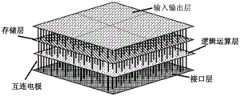
图1是本发明的系统结构示意图;Fig. 1 is a schematic diagram of the system structure of the present invention;
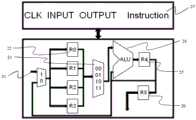
图2是本发明的逻辑架构框图和数据通路;Fig. 2 is a logical architecture block diagram and a data path of the present invention;
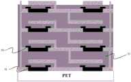
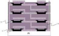
图3A与3B与3C是三种不同衬底上设计的三维堆叠结构的全透明微处理器的截面图;3A, 3B and 3C are cross-sectional views of fully transparent microprocessors with three-dimensional stacked structures designed on three different substrates;
图4A与4B与4C是三种不同设计的反相器;4A, 4B and 4C are inverters of three different designs;
图5是一种多路选择器(一位8路选择器)的设计;Fig. 5 is the design of a kind of multiplexer (one 8-way selector);
符号说明Symbol Description
21:输入线 22:初始寄存器组21: Input lines 22: Initial register set
23:4选1选择器 24:运算器单元ALU23: 4 to 1 selector 24: Arithmetic Unit ALU
25:运算寄存器 26:输出寄存器25: Operation register 26: Output register
27:指令、时钟模块 31:金属氧化物27: instruction, clock module 31: metal oxide
32:ITO材料 33:氧化铝材料32: ITO material 33: Aluminum oxide material
41:8个1位输入线 42:6条控制线41: 8 1-bit input lines 42: 6 control lines
43:一位输出线43: One bit output line
具体实施方式Detailed ways
下面结合附图和具体实施例对本发明作进一步详述。The present invention will be further described in detail below in conjunction with the accompanying drawings and specific embodiments.
本发明三维堆叠结构的全透明微处理器每层电路功能层均由薄膜晶体管基电路组成,不同功能层的电路由绝缘层隔开,不同层的互连通过刻蚀出通孔并沉积透明导电材料实现,相对传统技术,电路节省了75%的面积,降低了成本,也减小了电路互连的阻抗,提高了交互效率。如图1实例所示,该微处理器不同功能层主要包括有输入输出层、存储层、逻辑运算层以及接口层。每层电路均由金属氧化物作为有源层的薄膜晶体管构成。不同层之间通过沉积绝缘层氧化铝屏蔽,通过刻蚀通孔,沉积透明导电材料ITO实现片内互连。Each circuit functional layer of the fully transparent microprocessor with a three-dimensional stacked structure of the present invention is composed of thin film transistor-based circuits, circuits of different functional layers are separated by insulating layers, and the interconnections of different layers are etched through holes and deposited transparent conductive Material implementation, compared with traditional technology, the circuit saves 75% of the area, reduces the cost, also reduces the impedance of circuit interconnection, and improves the interaction efficiency. As shown in the example in Fig. 1, the different functional layers of the microprocessor mainly include an input and output layer, a storage layer, a logical operation layer and an interface layer. Each layer of circuit is composed of thin film transistors with metal oxide as the active layer. Different layers are shielded by depositing an insulating layer of aluminum oxide, through holes are etched, and transparent conductive material ITO is deposited to realize on-chip interconnection.
本发明的微处理器的架构通常如图2所示,主要包含多路选择器、运算器、寄存器等构成。在微处理器工作时,数据是从输入端2路选择器21选入,被选择性存入四个初始寄存器22中的一个。随后运算单元ALU24通过四路选择器23选择初始寄存器内存入的值进行取反等单值计算或与运算寄存器25的值进行加减乘除等双值运算。计算得到的值被存入运算寄存器25,根据指令可以被存入输出寄存器26中,也可以调用其进入运算单元执行计算,也可以调用其进入输入选择器模块,存入初始寄存器中。输入输出可以通过接口层与其他模块如传感器连接,实现传感器的感知和响应。运算所需的控制指令和时钟信号来自指令、时钟模块27。The architecture of the microprocessor of the present invention is generally shown in FIG. 2 , which mainly includes a multiplexer, an arithmetic unit, a register, and the like. When the microprocessor is working, the data is selected from the two-
如图3A、3B、3C所示,本发明主要针对不同需要设计了3种不同基底的三维堆叠结构的全透明微处理器。具体结构可以从截面中看到,ITO材料32构成薄膜晶体管的源漏极,金属氧化物31构成了薄膜晶体管的有源层,氧化铝33作为薄膜晶体管的有源层保护层和栅氧层,栅极依旧采用ITO材料32。在完成第一层电路的制作后,沉积氧化铝33作为不同层的屏蔽层,然后按照以上步骤再完成薄膜晶体管电路的沉积、退火以及制作,不同层的互连通过通孔沉积ITO材料32实现,重复以上步骤就可以实现三维堆叠的薄膜晶体管电路。针对不同应用的需要,三维堆叠的透明薄膜晶体管微处理器的基底可以选择图3A的铝硅玻璃、图3B的PET以及图3C的PI,图3A采用了耐刮抗摔的铝硅玻璃作为三维堆叠的全透明微处理器的基底,一方面能够实现非常好的透明度,另一方面玻璃基底极高的耐受温度能够使得微处理器有较高的制作工艺温度,进而让微处理器能够获得非常好的性能。图3B采用了透明度高、柔韧性好的PET材料作为三维堆叠的全透明微处理器的基底,能够满足穿戴设备所需的柔性,减小了外挂体积,增加了穿戴设备的舒适性,透明度高也使得其易于集成。图3C采用了透明度较好、柔性好、耐受温度高的PI材料作为三维堆叠的全透明微处理器的基底,在既能满足柔性和透明性的要求下,还能做到和铝硅玻璃类似的工艺温度,使得电路的电气性能得到提高。As shown in Figures 3A, 3B, and 3C, the present invention mainly designs fully transparent microprocessors with three-dimensional stacked structures on three different substrates for different needs. The specific structure can be seen from the cross section, the
本发明还提供一种具有特殊反相器的三维堆叠全透明微处理器,即其中的运算模块或其他需要缓冲或者反向的模块采用了如图4A所示的反相器,图4A、图4B和图4C分别展示了反馈型反相器、耗尽型负载反相器以及伪CMOS反相器。其中,depletion是耗尽型晶体管,enhancement是增强型晶体管。耗尽型晶体管是对增强型薄膜晶体管的有源层实施离子注入(如在等离子体增强化学的气相沉积设备中进行10分钟,功率65-70W的氘离子注入后得到)或紫外波长光源照射得到的。本发明设计的反相器(图4A)由四个薄膜晶体管构成,其中两个为增强型,两个为耗尽型;第一耗尽型晶体管漏极接电源,第二增强型晶体管栅极接输入,源极接地,漏极接第一耗尽型晶体管源极,第三耗尽型晶体管漏极接电源,栅极接第一耗尽型晶体管源极和第二增强型晶体管的漏极,源极接第一耗尽型晶体管栅极、第四增强型晶体管漏极共同接输出,第四增强型晶体管栅极接输入,源极接地。采用这种结构比常规的反相器具有更高增益和更大噪声容限,性能更佳,如表1。The present invention also provides a three-dimensional stacked fully transparent microprocessor with a special inverter, that is, the arithmetic module or other modules that need to be buffered or reversed adopt the inverter as shown in Figure 4A, Figure 4A, Figure 4A 4B and 4C show a feedback inverter, a depletion load inverter, and a pseudo-CMOS inverter, respectively. Among them, depletion is a depletion transistor, and enhancement is an enhancement transistor. The depletion mode transistor is obtained by ion implantation (such as deuterium ion implantation with a power of 65-70W in a plasma-enhanced chemical vapor deposition equipment for 10 minutes) or ultraviolet wavelength light source irradiation to the active layer of the enhanced thin film transistor. of. The inverter designed in the present invention (Fig. 4A) is made of four thin film transistors, two of them are enhancement type, two are depletion type; Connect to the input, the source is grounded, the drain is connected to the source of the first depletion-mode transistor, the drain of the third depletion-mode transistor is connected to the power supply, and the gate is connected to the source of the first depletion-mode transistor and the drain of the second enhancement-mode transistor , the source is connected to the gate of the first depletion transistor, the drain of the fourth enhancement transistor is connected to the output, the gate of the fourth enhancement transistor is connected to the input, and the source is grounded. Adopting this structure has higher gain and larger noise margin than the conventional inverter, and the performance is better, as shown in Table 1.
表1 三种反相器的参数比较Table 1 Comparison of parameters of three inverters

此外,本发明的微处理器还可以包括有如下的多路选择器,该多路选择器由多个增强型薄膜晶体管的阵列构成,栅极接控制信号,源极漏极作为数据传输线,利用透明薄膜晶体管的开关功能实现多路选择的功能。其中一个一位的8路选择器如图5所示。该多路选择器采用了增强型晶体管的开关功能实现。图5中的一位8路选择器,包括24个晶体管,8条1位输入线41,6条控制线42,一条一位输出线43。工作时,数据从8条1位输入线输入,6条控制线输入分别是一个三位控制指令及其反相后对应的值,这六个值与晶体管的栅极连接,当栅极是高电平时,晶体管的源漏导通,因此一个三位控制指令每次只能让8条链路中的一个链路上的晶体管全部导通,进而能够将输入值传输到输出值中,从而实现8路选择器的功能。In addition, the microprocessor of the present invention may also include the following multiplexer, the multiplexer is composed of a plurality of enhanced thin film transistor arrays, the gate is connected to the control signal, and the source and drain are used as data transmission lines. The switching function of the transparent thin film transistor realizes the function of multiple selection. One of the 8-way selectors is shown in Figure 5. The multiplexer is realized by using the switching function of the enhancement mode transistor. The one-bit 8-way selector in FIG. 5 includes 24 transistors, eight one-
以上所述,仅为本发明的具体实施方式,但本发明的保护范围并不局限于此,任何熟悉本技术领域的技术人员在本发明揭露的技术范围内,可轻易想到的变化或替换,都应涵盖在本发明的保护范围之内。因此,本发明的保护范围应以所述权利要求的保护范围为准。The above is only a specific embodiment of the present invention, but the scope of protection of the present invention is not limited thereto. Anyone skilled in the art can easily think of changes or substitutions within the technical scope disclosed in the present invention. All should be covered within the protection scope of the present invention. Therefore, the protection scope of the present invention should be determined by the protection scope of the claims.
Claims (7)
Translated fromChinesePriority Applications (1)
| Application Number | Priority Date | Filing Date | Title |
|---|---|---|---|
| CN202010326983.3ACN111477623B (en) | 2020-04-23 | 2020-04-23 | Three-dimensional stacked fully transparent microprocessor |
Applications Claiming Priority (1)
| Application Number | Priority Date | Filing Date | Title |
|---|---|---|---|
| CN202010326983.3ACN111477623B (en) | 2020-04-23 | 2020-04-23 | Three-dimensional stacked fully transparent microprocessor |
Publications (2)
| Publication Number | Publication Date |
|---|---|
| CN111477623A CN111477623A (en) | 2020-07-31 |
| CN111477623Btrue CN111477623B (en) | 2023-06-16 |
Family
ID=71763429
Family Applications (1)
| Application Number | Title | Priority Date | Filing Date |
|---|---|---|---|
| CN202010326983.3AActiveCN111477623B (en) | 2020-04-23 | 2020-04-23 | Three-dimensional stacked fully transparent microprocessor |
Country Status (1)
| Country | Link |
|---|---|
| CN (1) | CN111477623B (en) |
Citations (3)
| Publication number | Priority date | Publication date | Assignee | Title |
|---|---|---|---|---|
| CN105162463A (en)* | 2015-09-26 | 2015-12-16 | 浙江大学 | Low-phase-noise self-injection voltage-controlled oscillator for 60GHz phase-locked loop and wireless transceiver |
| CN109410888A (en)* | 2018-09-14 | 2019-03-01 | 浙江大学 | A kind of transparent differential operational amplifier based on thin film transistor (TFT) |
| WO2019066872A1 (en)* | 2017-09-28 | 2019-04-04 | Intel Corporation | Monolithic integration of a thin film transistor over a complimentary transistor |
Family Cites Families (7)
| Publication number | Priority date | Publication date | Assignee | Title |
|---|---|---|---|---|
| US6271542B1 (en)* | 1997-12-08 | 2001-08-07 | International Business Machines Corporation | Merged logic and memory combining thin film and bulk Si transistors |
| TWI316760B (en)* | 2006-05-03 | 2009-11-01 | Ind Tech Res Inst | Circuit structure with doubl-gate organic thin film transistors and application thereof |
| KR102045730B1 (en)* | 2012-12-28 | 2019-12-03 | 엘지디스플레이 주식회사 | Inverter and driving circuit and display device using the same |
| CN107305594B (en)* | 2016-04-22 | 2021-01-08 | 杭州海存信息技术有限公司 | A processor with a three-dimensional storage array |
| US10381068B2 (en)* | 2017-12-20 | 2019-08-13 | International Business Machines Corporation | Ultra dense and stable 4T SRAM cell design having NFETs and PFETs |
| CN108831400A (en)* | 2018-07-26 | 2018-11-16 | 深圳市华星光电技术有限公司 | Liquid crystal display panel and its driving method including GOA circuit |
| CN109993243A (en)* | 2019-03-05 | 2019-07-09 | 浙江大学 | A product anti-counterfeiting traceability system based on transparent film RFID chip |
- 2020
- 2020-04-23CNCN202010326983.3Apatent/CN111477623B/enactiveActive
Patent Citations (3)
| Publication number | Priority date | Publication date | Assignee | Title |
|---|---|---|---|---|
| CN105162463A (en)* | 2015-09-26 | 2015-12-16 | 浙江大学 | Low-phase-noise self-injection voltage-controlled oscillator for 60GHz phase-locked loop and wireless transceiver |
| WO2019066872A1 (en)* | 2017-09-28 | 2019-04-04 | Intel Corporation | Monolithic integration of a thin film transistor over a complimentary transistor |
| CN109410888A (en)* | 2018-09-14 | 2019-03-01 | 浙江大学 | A kind of transparent differential operational amplifier based on thin film transistor (TFT) |
Non-Patent Citations (3)
| Title |
|---|
| Low-Power Transparent RFID Circuits Using Enhancement/Depletion Logic Gates Based on Deuterium-Treated ZnO TFTs;Hua Xu等;IEEE ELECTRON DEVICE LETTERS;第38卷(第10期);1383-1386* |
| 氧化锌锡薄膜晶体管的研究;王雄;才玺坤;原子健;朱夏明;邱东江;吴惠桢;;物理学报(第03期);636-639* |
| 采用耗尽型负载元件的高性能n-沟MOS大规模集成电路;刘鹿生;微电子学动态;33-42* |
Also Published As
| Publication number | Publication date |
|---|---|
| CN111477623A (en) | 2020-07-31 |
Similar Documents
| Publication | Publication Date | Title |
|---|---|---|
| CN101997539B (en) | Programmable logic circuit | |
| CN111477623B (en) | Three-dimensional stacked fully transparent microprocessor | |
| El-Bendary et al. | Efficient multiple 4-Bit ALU designs for fast computation and reduced area | |
| WO2021121107A1 (en) | Logic circuit design method | |
| Keerthana et al. | Implementation of Low Power 1-bit Hybrid Full Adder using 22 nm CMOS Technology | |
| CN104407835A (en) | Three-dimensional quantum cellular automata adder | |
| US7570081B1 (en) | Multiple-output static logic | |
| US20120250817A1 (en) | vMOS Multi-valued Counter Unit | |
| CN103631560B (en) | 4 bit array multipliers based on reversible logic | |
| Hashimoto et al. | 33.3 Via-Switch FPGA: 65nm CMOS Implementation and Architecture Extension for Al Applications | |
| CN116827334B (en) | A four-variable original code to complement circuit based on memristor | |
| Ramana et al. | An Efficient Approach to Design Ternary Logic Circuits with GNRFETs | |
| Vella et al. | Performance evaluation of various cmos designs for signal processing applications | |
| Dhanasekar et al. | Design and Analysis of Multipliers using Hybrid Full Adder | |
| CN101799747B (en) | Arithmetic logic unit ALU based on reversible logic | |
| CN111294040B (en) | Reconfigurable combinational logic unit based on static circuit | |
| CN114741050A (en) | Full-addition circuit, high carry circuit and adder based on memristor and CMOS transistor | |
| CN203324967U (en) | Threshold logic type carry lookahead adder comprising SET/MOS (Single Electron Transistor/Metal Oxide Semiconductor) hybrid circuit | |
| KR20230115095A (en) | one-bit full adder | |
| CN220305789U (en) | Low-power-consumption full adder based on basic gate circuit | |
| Bhuvaneshwari et al. | Low Power CMOS GDI Full-adder Design | |
| Sarker et al. | Design and Comparative Analysis of 1-BIT ALU and Full Adder using MGDI Technique for High-Performance PLC Applications | |
| Kumar | Low Power Hybrid Full Adder Design using MGDI Based XNOR Gate with Swing Restored Technique | |
| Priyadarshini et al. | Comparative analysis of a low power and high speed hybrid 1-bit full adder for ULSI circuits | |
| Priyanka et al. | Design Of GDI Based 4-Bit Multiplier Using Low Power Adder Cells |
Legal Events
| Date | Code | Title | Description |
|---|---|---|---|
| PB01 | Publication | ||
| PB01 | Publication | ||
| SE01 | Entry into force of request for substantive examination | ||
| SE01 | Entry into force of request for substantive examination | ||
| GR01 | Patent grant | ||
| GR01 | Patent grant |