CN111463652A - light-emitting device - Google Patents
light-emitting deviceDownload PDFInfo
- Publication number
- CN111463652A CN111463652ACN201910057364.6ACN201910057364ACN111463652ACN 111463652 ACN111463652 ACN 111463652ACN 201910057364 ACN201910057364 ACN 201910057364ACN 111463652 ACN111463652 ACN 111463652A
- Authority
- CN
- China
- Prior art keywords
- light
- emitting device
- conductive pad
- adhesive layer
- substrate structure
- Prior art date
- Legal status (The legal status is an assumption and is not a legal conclusion. Google has not performed a legal analysis and makes no representation as to the accuracy of the status listed.)
- Pending
Links
- 239000000758substrateSubstances0.000claimsabstractdescription50
- 239000012790adhesive layerSubstances0.000claimsabstractdescription25
- 238000004806packaging method and processMethods0.000claimsabstract9
- 239000008393encapsulating agentSubstances0.000claimsdescription20
- 239000010410layerSubstances0.000claimsdescription19
- 230000005693optoelectronicsEffects0.000claimsdescription13
- 239000000463materialSubstances0.000claimsdescription8
- 230000003287optical effectEffects0.000claimsdescription4
- 229920006332epoxy adhesivePolymers0.000claimsdescription3
- 239000013464silicone adhesiveSubstances0.000claimsdescription3
- -1acrylChemical group0.000claims1
- 239000000853adhesiveSubstances0.000claims1
- 230000001070adhesive effectEffects0.000claims1
- 238000004519manufacturing processMethods0.000abstractdescription8
- 238000005538encapsulationMethods0.000description14
- 230000003647oxidationEffects0.000description6
- 238000007254oxidation reactionMethods0.000description6
- PXHVJJICTQNCMI-UHFFFAOYSA-NNickelChemical compound[Ni]PXHVJJICTQNCMI-UHFFFAOYSA-N0.000description4
- 238000000034methodMethods0.000description4
- RYGMFSIKBFXOCR-UHFFFAOYSA-NCopperChemical compound[Cu]RYGMFSIKBFXOCR-UHFFFAOYSA-N0.000description2
- VYPSYNLAJGMNEJ-UHFFFAOYSA-NSilicium dioxideChemical compoundO=[Si]=OVYPSYNLAJGMNEJ-UHFFFAOYSA-N0.000description2
- ATJFFYVFTNAWJD-UHFFFAOYSA-NTinChemical compound[Sn]ATJFFYVFTNAWJD-UHFFFAOYSA-N0.000description2
- GWEVSGVZZGPLCZ-UHFFFAOYSA-NTitan oxideChemical compoundO=[Ti]=OGWEVSGVZZGPLCZ-UHFFFAOYSA-N0.000description2
- 239000003522acrylic cementSubstances0.000description2
- 229910052782aluminiumInorganic materials0.000description2
- XAGFODPZIPBFFR-UHFFFAOYSA-NaluminiumChemical compound[Al]XAGFODPZIPBFFR-UHFFFAOYSA-N0.000description2
- 230000000903blocking effectEffects0.000description2
- 229910052802copperInorganic materials0.000description2
- 239000010949copperSubstances0.000description2
- 230000000694effectsEffects0.000description2
- 238000009713electroplatingMethods0.000description2
- 238000000465mouldingMethods0.000description2
- 229910052759nickelInorganic materials0.000description2
- 229910052718tinInorganic materials0.000description2
- 239000004925Acrylic resinSubstances0.000description1
- 229920000178Acrylic resinPolymers0.000description1
- OAICVXFJPJFONN-UHFFFAOYSA-NPhosphorusChemical compound[P]OAICVXFJPJFONN-UHFFFAOYSA-N0.000description1
- XUIMIQQOPSSXEZ-UHFFFAOYSA-NSiliconChemical compound[Si]XUIMIQQOPSSXEZ-UHFFFAOYSA-N0.000description1
- 230000004075alterationEffects0.000description1
- 239000000919ceramicSubstances0.000description1
- 229910052681coesiteInorganic materials0.000description1
- 239000000084colloidal systemSubstances0.000description1
- 229910052906cristobaliteInorganic materials0.000description1
- 230000003247decreasing effectEffects0.000description1
- 230000002950deficientEffects0.000description1
- 239000003822epoxy resinSubstances0.000description1
- 238000001125extrusionMethods0.000description1
- 239000011521glassSubstances0.000description1
- 229910052751metalInorganic materials0.000description1
- 239000002184metalSubstances0.000description1
- 239000002245particleSubstances0.000description1
- 229920000647polyepoxidePolymers0.000description1
- 229910052594sapphireInorganic materials0.000description1
- 239000010980sapphireSubstances0.000description1
- 229910052710siliconInorganic materials0.000description1
- 239000010703siliconSubstances0.000description1
- 239000000377silicon dioxideSubstances0.000description1
- 235000012239silicon dioxideNutrition0.000description1
- 229920002050silicone resinPolymers0.000description1
- 229910052682stishoviteInorganic materials0.000description1
- 238000006467substitution reactionMethods0.000description1
- 229910052905tridymiteInorganic materials0.000description1
Images


Classifications
- H—ELECTRICITY
- H01—ELECTRIC ELEMENTS
- H01S—DEVICES USING THE PROCESS OF LIGHT AMPLIFICATION BY STIMULATED EMISSION OF RADIATION [LASER] TO AMPLIFY OR GENERATE LIGHT; DEVICES USING STIMULATED EMISSION OF ELECTROMAGNETIC RADIATION IN WAVE RANGES OTHER THAN OPTICAL
- H01S5/00—Semiconductor lasers
- H01S5/02—Structural details or components not essential to laser action
- H01S5/0206—Substrates, e.g. growth, shape, material, removal or bonding
- H—ELECTRICITY
- H01—ELECTRIC ELEMENTS
- H01S—DEVICES USING THE PROCESS OF LIGHT AMPLIFICATION BY STIMULATED EMISSION OF RADIATION [LASER] TO AMPLIFY OR GENERATE LIGHT; DEVICES USING STIMULATED EMISSION OF ELECTROMAGNETIC RADIATION IN WAVE RANGES OTHER THAN OPTICAL
- H01S5/00—Semiconductor lasers
- H01S5/02—Structural details or components not essential to laser action
- H01S5/022—Mountings; Housings
- H01S5/0225—Out-coupling of light
- H01S5/02253—Out-coupling of light using lenses
- H—ELECTRICITY
- H01—ELECTRIC ELEMENTS
- H01S—DEVICES USING THE PROCESS OF LIGHT AMPLIFICATION BY STIMULATED EMISSION OF RADIATION [LASER] TO AMPLIFY OR GENERATE LIGHT; DEVICES USING STIMULATED EMISSION OF ELECTROMAGNETIC RADIATION IN WAVE RANGES OTHER THAN OPTICAL
- H01S5/00—Semiconductor lasers
- H01S5/04—Processes or apparatus for excitation, e.g. pumping, e.g. by electron beams
- H01S5/042—Electrical excitation ; Circuits therefor
- H—ELECTRICITY
- H01—ELECTRIC ELEMENTS
- H01S—DEVICES USING THE PROCESS OF LIGHT AMPLIFICATION BY STIMULATED EMISSION OF RADIATION [LASER] TO AMPLIFY OR GENERATE LIGHT; DEVICES USING STIMULATED EMISSION OF ELECTROMAGNETIC RADIATION IN WAVE RANGES OTHER THAN OPTICAL
- H01S5/00—Semiconductor lasers
- H01S5/10—Construction or shape of the optical resonator, e.g. extended or external cavity, coupled cavities, bent-guide, varying width, thickness or composition of the active region
- H01S5/18—Surface-emitting [SE] lasers, e.g. having both horizontal and vertical cavities
- H01S5/183—Surface-emitting [SE] lasers, e.g. having both horizontal and vertical cavities having only vertical cavities, e.g. vertical cavity surface-emitting lasers [VCSEL]
Landscapes
- Physics & Mathematics (AREA)
- Condensed Matter Physics & Semiconductors (AREA)
- General Physics & Mathematics (AREA)
- Electromagnetism (AREA)
- Optics & Photonics (AREA)
- Led Device Packages (AREA)
Abstract
Description
Translated fromChinese技术领域technical field
本揭示内容是关于一种发光装置。The present disclosure relates to a light emitting device.
背景技术Background technique
垂直共振腔面射型激光(Vertical-Cavity Surface-Emitting Laser,VCSEL)二极管为近年来常见的点光源。包含VCSEL二极管的发光装置具有许多优点,例如较低的能量消耗、较长的寿命、更小的尺寸与更快的开关切换速度。Vertical-Cavity Surface-Emitting Laser (VCSEL) diodes are a common point light source in recent years. Lighting devices incorporating VCSEL diodes have many advantages, such as lower power consumption, longer lifetime, smaller size, and faster switching speeds.
现行的发光装置通常包括围绕VCSEL二极管的反射杯体及上盖,其中反射杯体与上盖之间透过胶体粘结在一起。然而,反射杯体与VCSEL二极管之间需间隔一适当距离,以避免因制程公差导致在装设反射杯体时挤压到导线。因此,发光装置的大小受限于反射杯体,而无法有效地减小。Existing light-emitting devices generally include a reflective cup body and an upper cover surrounding the VCSEL diode, wherein the reflective cup body and the upper cover are bonded together through colloid. However, an appropriate distance is required between the reflector cup and the VCSEL diode to avoid pinching the wires when the reflector cup is installed due to process tolerances. Therefore, the size of the light-emitting device is limited by the reflection cup and cannot be effectively reduced.
发明内容SUMMARY OF THE INVENTION
本揭示内容的一态样是提供一种发光装置,包括基板结构、垂直共振腔面射型激光二极管、第一导线、封装胶层、透镜元件、以及空气间隙。基板结构包含基板、第一导电垫、以及第二导电垫。垂直共振腔面射型激光二极管设置于基板结构上,并与第一导电垫电性连接。第一导线电性连接垂直共振腔面射型激光二极管与第二导电垫。封装胶层覆盖垂直共振腔面射型激光二极管、第一导线、以及基板结构。透镜元件设置于封装胶层之上。空气间隙位于透镜元件与封装胶层之间。An aspect of the present disclosure is to provide a light emitting device including a substrate structure, a vertical resonant cavity surface-emitting laser diode, a first wire, an encapsulant layer, a lens element, and an air gap. The substrate structure includes a substrate, a first conductive pad, and a second conductive pad. The vertical resonant cavity surface-emitting laser diode is arranged on the substrate structure and is electrically connected with the first conductive pad. The first wire is electrically connected to the vertical resonant cavity surface-emitting laser diode and the second conductive pad. The encapsulation adhesive layer covers the vertical resonant cavity surface-emitting laser diode, the first wire, and the substrate structure. The lens element is arranged on the encapsulation adhesive layer. An air gap is located between the lens element and the encapsulant layer.
在本揭示内容的一实施方式中,透镜元件包含载体及透镜阵列。透镜阵列设置于载体下,且透镜阵列包含多个透镜。In one embodiment of the present disclosure, the lens element includes a carrier and a lens array. The lens array is disposed under the carrier, and the lens array includes a plurality of lenses.
在本揭示内容的一实施方式中,各透镜具有球形表面,且球形表面面向封装胶层。In one embodiment of the present disclosure, each lens has a spherical surface, and the spherical surface faces the encapsulant layer.
在本揭示内容的一实施方式中,封装胶层与所述多个透镜具有实质上相同的折射率。In one embodiment of the present disclosure, the encapsulant layer and the plurality of lenses have substantially the same refractive index.
在本揭示内容的一实施方式中,透镜元件还包含支撑件。支撑件接触载体及封装胶层,且支撑件的高度高于所述多个透镜的高度。In one embodiment of the present disclosure, the lens element further includes a support. The support member contacts the carrier and the encapsulation adhesive layer, and the height of the support member is higher than that of the plurality of lenses.
在本揭示内容的一实施方式中,支撑件包括硅胶粘着剂、环氧树脂粘着剂、压克力胶粘着剂或其组合。In one embodiment of the present disclosure, the support includes a silicone adhesive, an epoxy adhesive, an acrylic adhesive, or a combination thereof.
在本揭示内容的一实施方式中,支撑件围绕透镜阵列,从而形成空气间隙。In an embodiment of the present disclosure, the support surrounds the lens array, thereby forming an air gap.
在本揭示内容的一实施方式中,封装胶层掺杂有光学材料。In one embodiment of the present disclosure, the encapsulant layer is doped with an optical material.
在本揭示内容的一实施方式中,发光装置进一步包括光电元件。光电元件设置于基板结构上,并被封装胶层所覆盖。In an embodiment of the present disclosure, the light emitting device further includes a photovoltaic element. The photoelectric element is arranged on the substrate structure and covered by the encapsulation adhesive layer.
在本揭示内容的一实施方式中,发光装置进一步包括第二导线,且基板结构还包括第三导电垫及第四导电垫。光电元件与第三导电垫电性连接,且第二导线电性连接光电元件与第四导电垫。In an embodiment of the present disclosure, the light emitting device further includes a second wire, and the substrate structure further includes a third conductive pad and a fourth conductive pad. The optoelectronic element is electrically connected to the third conductive pad, and the second wire is electrically connected to the optoelectronic element and the fourth conductive pad.
由上述实施方式可知,本发明提供一种发光装置。在此发光装置中,以封装胶层取代了反射杯体,因此有效地缩小发光装置的尺寸,并阻隔水气及避免氧化及剥离情况的发生。再者,相较于先前技术,本发明的发光装置的制造制程较简化,减少了制程工序并降低生产成本。此外,本发明的发光装置还可包含光电元件,确保发光装置的安全性,避免对人眼的安全造成危害。As can be seen from the above embodiments, the present invention provides a light-emitting device. In this light-emitting device, the reflective cup is replaced by an encapsulating adhesive layer, thereby effectively reducing the size of the light-emitting device, blocking moisture and avoiding the occurrence of oxidation and peeling. Furthermore, compared with the prior art, the manufacturing process of the light-emitting device of the present invention is simplified, which reduces the manufacturing process and reduces the production cost. In addition, the light-emitting device of the present invention may further include optoelectronic elements to ensure the safety of the light-emitting device and avoid harm to the safety of human eyes.
以下将以实施方式对上述的说明作详细的描述,并对本揭示内容的技术方案提供更进一步的解释。The above description will be described in detail in the following embodiments, and further explanations will be provided for the technical solutions of the present disclosure.
附图说明Description of drawings
当结合附图阅读时,从以下详细描述中可以更好地理解本揭露的各个方面。应注意,依据工业中的标凖实务,多个特征并未按比例绘制。实际上,多个特征的尺寸可任意增大或缩小,以便使论述明晰。Various aspects of the present disclosure may be better understood from the following detailed description when read in conjunction with the accompanying drawings. It should be noted that in accordance with standard practice in the industry, various features are not drawn to scale. In fact, the dimensions of the various features may be arbitrarily increased or decreased in order to clarify the discussion.
图1A绘示根据本揭示内容的一些实施方式的发光装置的立体示意图;FIG. 1A is a schematic perspective view of a light-emitting device according to some embodiments of the present disclosure;
图1B绘示根据本揭示内容的一些实施方式的发光装置的侧视示意图;FIG. 1B is a schematic side view of a light emitting device according to some embodiments of the present disclosure;
图1C绘示根据本揭示内容的一些实施方式的发光装置的上视示意图;1C is a schematic top view of a light emitting device according to some embodiments of the present disclosure;
图1D绘示根据本揭示内容的一些实施方式的发光装置的下视示意图;1D is a schematic bottom view of a light-emitting device according to some embodiments of the present disclosure;
图2A绘示根据本揭示内容的一些实施方式的发光装置的立体示意图;2A is a schematic perspective view of a light-emitting device according to some embodiments of the present disclosure;
图2B绘示根据本揭示内容的一些实施方式的发光装置的爆炸示意图;2B is a schematic exploded view of a light-emitting device according to some embodiments of the present disclosure;
图2C绘示根据本揭示内容的一些实施方式的发光装置的侧视示意图;2C is a schematic side view of a light-emitting device according to some embodiments of the present disclosure;
图2D绘示根据本揭示内容的一些实施方式的发光装置的上视示意图;2D illustrates a schematic top view of a light-emitting device according to some embodiments of the present disclosure;
图2E绘示根据本揭示内容的一些实施方式的发光装置的下视示意图。2E is a schematic bottom view of a light emitting device according to some embodiments of the present disclosure.
具体实施方式Detailed ways
以下揭示内容提供许多不同实施例或实例以用于实现所提供标的物的不同的特征。下文描述组件及排列的特定实例以简化本揭露。当然,这些仅仅为实例,并不旨在限制本揭露。举例而言,在随后描述中的在第二特征之上或在第二特征上形成第一特征可包括形成直接接触的第一特征和第二特征的实施例,还可以包括在第一特征和第二特征之间形成额外特征,从而使第一特征和第二特征不直接接触的实施例。另外,本揭露在各实例中可重复元件符号及/或字母。此重复是出于简化及清楚的目的,且本身不指示所论述各实施例及/或构造之间的关系。The following disclosure provides many different embodiments or examples for implementing different features of the provided subject matter. Specific examples of components and arrangements are described below to simplify the present disclosure. Of course, these are only examples and are not intended to limit the present disclosure. By way of example, embodiments in the ensuing description where forming a first feature over or on a second feature may include forming direct contact between the first feature and the second feature may also include embodiments where the first feature and the second feature are in direct contact. Embodiments in which additional features are formed between the second features so that the first and second features are not in direct contact. Additionally, the present disclosure may repeat reference numerals and/or letters throughout the examples. This repetition is for the purpose of simplicity and clarity, and does not in itself indicate a relationship between the various embodiments and/or configurations discussed.
另外,空间相对用语,诸如“下方”、“以下”、“下部”、“上方”、“上部”及类似者,在此用于简化描述附图所示的一个元件或特征与另一元件(或多个元件)或特征(或多个特征)的关系。除附图中描绘的方向外,空间相对用语旨在包含于使用或操作中的装置的不同方向。装置可为不同的方向(旋转90度或在其他的方向),并且在此使用的空间相关描述词也可相应地被解释。In addition, spatially relative terms, such as "below," "below," "lower," "above," "upper," and the like, are used herein to simplify the description of one element or feature shown in the figures compared to another element ( or elements) or feature (or features). In addition to the orientation depicted in the figures, spatially relative terms are intended to encompass different orientations of the device in use or operation. The device may be oriented in different directions (rotated 90 degrees or at other orientations) and the spatially relative descriptors used herein interpreted accordingly.
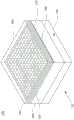
请参照图1A、图1B、图1C、以及图1D。图1A绘示根据本揭示内容的一些实施方式的发光装置10a的立体示意图,图1B、图1C、以及图1D则分别绘示发光装置10a的侧视示意图、上视示意图、以及下视示意图。如图1A、图1B、图1C、以及图1D所示,发光装置10a包括基板结构100、垂直共振腔面射型激光(Vertical-Cavity Surface-Emitting Laser,VCSEL)二极管200、第一导线310、封装胶层400、以及透镜元件500。Please refer to FIG. 1A , FIG. 1B , FIG. 1C , and FIG. 1D . 1A is a schematic three-dimensional view of a light-emitting
基板结构100包含基板110、第一导电垫120、以及第二导电垫130。基板110可以包含任何合适的基板。在某些实施方式中,基板110可以为透明基板或不透明基板。在某些实施方式中,基板110可以为软性基板。在其他实施方式中,基板110可以为刚性基板。例如,基板110可以为蓝宝石基板、硅基板、玻璃基板、印刷电路板、金属基板或陶瓷基板等,但不以此为限。The
第一导电垫120及第二导电垫130可透过例如模具成型、贴附或电镀等方式,形成在基板110上。在一些实施例中,第一导电垫120及第二导电垫130可包括铜、铝、镍、锡或前述的组合,但不以此为限。应理解的是,虽然在图1A~图1D中,第一导电垫120及第二导电垫130是设置于基板110的上表面上,但在某些实施方式中,第一导电垫120及第二导电垫130亦可嵌置于基板中,并与基板110的上表面齐平。The first
VCSEL二极管200设置于基板结构100上,并与第一导电垫120及第二导电垫130电性连接。具体地,如图1A及图1B所示,VCSEL二极管200可设置于第一导电垫120上,并通过打线接合(wire bonding)方式,通过第一导线310电性连接至第二导电垫130,以形成回路。值得一提的是,虽然在本实施方式中,发光装置10a具有两条第一导线310(如图1A及图1C所示),但本发明不限于此。例如,当一条导线即可供应VCSEL二极管200足够的电流时,发光装置10a亦可仅具有一条第一导线310。The
封装胶层400覆盖VCSEL二极管200、第一导线310、以及基板结构100。据此,封装胶层400可阻隔水气,并避免第一导电垫120、第二导电垫130、以及第一导线310的氧化。另一方面,封装胶层400亦可保护VCSEL二极管200与第一导电垫120之间的接合,以及第一导线310与VCSEL二极管200或第二导电垫130之间的接合,从而避免剥离情况的发生。在一些实施例中,封装胶层400包括硅氧树脂、环氧树脂或压克力树脂,但不以此为限。The
如先前技术所述,在目前现有的VCSEL二极管发光装置中,反射杯体与VCSEL二极管之间需间隔一适当距离,以避免因制程公差导致在装设反射杯体时挤压到导线。因此,现有的VCSEL二极管发光装置的大小受限于反射杯体,而无法有效地减小。相较于上述先前技术所遇到的困难,在此揭露的发光装置10a中,以封装胶层400取代了反射杯体,因此可有效缩小装置的尺寸。举例来说,以约1毫米×1毫米大小的VCSEL二极管为例,包含此大小的VCSEL二极管的本发明的发光装置的大小可仅为约1.6毫米×1.6毫米。此外,亦可通过封装胶层400的设置,达到上述的避免氧化及剥离情况的功效。As described in the prior art, in the existing VCSEL diode light-emitting device, an appropriate distance is required between the reflector cup and the VCSEL diode to avoid extrusion of the wires when the reflector cup is installed due to process tolerances. Therefore, the size of the existing VCSEL diode light-emitting device is limited by the reflection cup, and cannot be effectively reduced. Compared with the above-mentioned difficulties encountered in the prior art, in the light-emitting
在一些实施方式中,封装胶层400可掺杂有光学材料。光学材料可为波长转换材料或散射材料。在一些实施例中,波长转换材料例如是荧光粉。在一些实施例中,散射材料例如是SiO2、TiO2等散射粒子。In some embodiments, the
透镜元件500设置于封装胶层400之上。具体地,透镜元件500包含载体510及透镜阵列520。透镜阵列520设置于载体510下,且包含多个透镜521。如图1B所示,各透镜521具有球形表面,且球形表面面向封装胶层400。据此,透镜阵列520配置以用于改变出光的角度及提高出光的均匀性。The
需注意的是,发光装置10a还包括空气间隙600。空气间隙600位于透镜元件500与封装胶层400之间。详言之,透镜元件500包括支撑件530。支撑件530的底部接触封装胶层400,且支撑件530的顶部接触并支撑载体510。更详细而言之,支撑件530围绕出一空间以容纳透镜阵列520。如图1C所示,支撑件530的俯视轮廓为“中空矩形”(或“口字型”),但本发明不以此为限。在一些实施方式中,支撑件530的高度H1高于透镜521的高度H2(如图1B所示)。据此,封装胶层400、透镜阵列520、以及支撑件530界定出空气间隙600。It should be noted that the
通过支撑件530的设置,使透镜阵列520与封装胶层400通过空气间隙600而间隔开,可有效地提高装置出光的均匀性。详细而言,当封装胶层400与透镜521具有实质上相同或近似的折射率时,若封装胶层400接触到透镜阵列520或甚至与透镜阵列520密合,则透镜阵列520将无法有效地改变出光角度及提高出光的均匀性。在一些实施方式中,支撑件530包括硅胶粘着剂、环氧树脂粘着剂、压克力胶粘着剂或其组合,但不以此为限。Through the disposition of the
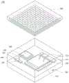
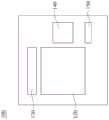
请参照图2A、图2B、图2C、图2D、以及图2E。图2A绘示根据本揭示内容的另一些实施方式的发光装置10b的立体示意图。图2B绘示发光装置10b的爆炸示意图。图2C绘示发光装置10b从图2A的方向D1观看的侧视示意图。图2D及图2E分别绘示发光装置10b的上视示意图、以及下视示意图。须说明的是,在图2A~图2E中,与图1A~图1D中相同或相似的元件被给予相同的符号,并省略相关说明。图2A~图2E的发光装置10b与图1A~图1D的发光装置10a相似,差异在发光装置10b进一步包括光电元件700。Please refer to FIGS. 2A , 2B, 2C, 2D, and 2E. FIG. 2A is a schematic perspective view of a
当发光装置10b用于人脸辨识时,通过光电元件700的设置,可确保发光装置10b的安全性,避免对人眼的安全造成危害。具体而言,若透镜元件500破损(例如其中一些透镜521脱落),则VCSEL二极管200发射的红外光通过破损位置直接照射人眼,可能会对人眼造成伤害。因此,通过光电元件700的设置,光电元件700可即时侦测经透镜元件500反射回来的光,以辨别透镜元件500是否有破损或瑕疵。When the
如图2A~图2E所示,光电元件700设置于基板结构100上,并被封装胶层400所覆盖。具体地,基板结构100还包括第三导电垫140及第四导电垫150。第三导电垫140及第四导电垫150可透过例如模具成型、贴附或电镀等方式,形成在基板110上。在一些实施例中,第三导电垫140及第四导电垫150可包括铜、铝、镍、锡或前述的组合,但不以此为限。应理解的是,虽然在图2A~图2E中,第三导电垫140及第四导电垫150是设置于基板110的上表面上,但在某些实施方式中,第三导电垫140及第四导电垫150亦可嵌置于基板中,并与基板110的上表面齐平。As shown in FIGS. 2A to 2E , the
如图2A~图2E所示,发光装置10b进一步包括第二导线320。光电元件700与第三导电垫140电性连接,且第二导线320电性连接光电元件700与第四导电垫150。具体地,光电元件700可设置于第三导电垫140上,并通过打线接合(wire bonding)方式,通过第二导线320电性连接至第四导电垫150,以形成回路。As shown in FIGS. 2A to 2E , the
在本实施方式中,封装胶层400亦覆盖光电元件700、第二导线320、第三导电垫140、以及第四导电垫150。因此,封装胶层400亦可避免第二导线320、第三导电垫140、以及第四导电垫150的氧化。另一方面,封装胶层400亦可保护光电元件700与第三导电垫140之间的接合,以及第二导线320与光电元件700或第四导电垫150之间的接合,从而避免剥离情况的发生。In this embodiment, the
如上所述,相较于先前技术,在此揭露的发光装置10b中,以封装胶层400取代了反射杯体,因此可有效缩小装置的尺寸。举例来说,包含约1毫米×1毫米大小的VCSEL二极管及光电元件的本发明的发光装置的大小可仅为约2.0毫米×2.0毫米。此外,亦可通过封装胶层400的设置,达到上述的避免氧化及剥离情况的功效。As mentioned above, compared with the prior art, in the
由上述发明实施例可知,在此揭露的发光装置中,以封装胶层取代了反射杯体,因此有效地缩小发光装置的尺寸,并阻隔水气及避免氧化及剥离情况的发生。再者,相较于先前技术,本发明的发光装置的制造制程较简化,减少了制程工序并降低生产成本。此外,本发明的发光装置还可包含光电元件,确保发光装置的安全性,避免对人眼的安全造成危害。As can be seen from the above embodiments of the invention, in the light-emitting device disclosed herein, the reflective cup is replaced by an encapsulating adhesive layer, thereby effectively reducing the size of the light-emitting device, blocking moisture, and preventing oxidation and peeling. Furthermore, compared with the prior art, the manufacturing process of the light-emitting device of the present invention is simplified, which reduces the manufacturing process and reduces the production cost. In addition, the light-emitting device of the present invention may further include optoelectronic elements to ensure the safety of the light-emitting device and avoid harm to the safety of human eyes.
上文概述若干实施例的特征,使得熟悉此项技术者可更好地理解本揭露的态样。熟悉此项技术者应了解,可轻易使用本揭露作为设计或修改其他制程及结构的基础,以便实施本文所介绍的实施例的相同目的及/或实现相同优势。熟悉此项技术者亦应认识到,此类等效结构并未脱离本揭露的精神及范畴,且可在不脱离本揭露的精神及范畴的情况下产生本文的各种变化、替代及更改。The foregoing outlines the features of several embodiments so that those skilled in the art may better understand aspects of the present disclosure. Those skilled in the art should appreciate that the present disclosure may be readily utilized as a basis for designing or modifying other processes and structures for carrying out the same purposes and/or achieving the same advantages of the embodiments described herein. Those skilled in the art should also realize that such equivalent structures do not depart from the spirit and scope of the present disclosure, and that various changes, substitutions and alterations herein can be made without departing from the spirit and scope of the present disclosure.
Claims (10)
Priority Applications (1)
| Application Number | Priority Date | Filing Date | Title |
|---|---|---|---|
| CN201910057364.6ACN111463652A (en) | 2019-01-22 | 2019-01-22 | light-emitting device |
Applications Claiming Priority (1)
| Application Number | Priority Date | Filing Date | Title |
|---|---|---|---|
| CN201910057364.6ACN111463652A (en) | 2019-01-22 | 2019-01-22 | light-emitting device |
Publications (1)
| Publication Number | Publication Date |
|---|---|
| CN111463652Atrue CN111463652A (en) | 2020-07-28 |
Family
ID=71679120
Family Applications (1)
| Application Number | Title | Priority Date | Filing Date |
|---|---|---|---|
| CN201910057364.6APendingCN111463652A (en) | 2019-01-22 | 2019-01-22 | light-emitting device |
Country Status (1)
| Country | Link |
|---|---|
| CN (1) | CN111463652A (en) |
Citations (16)
| Publication number | Priority date | Publication date | Assignee | Title |
|---|---|---|---|---|
| US5997185A (en)* | 1996-01-09 | 1999-12-07 | Siemens Aktiengesellschaft | Optoelectronic transmit module |
| JP2007049017A (en)* | 2005-08-11 | 2007-02-22 | Ricoh Co Ltd | Photoelectric conversion module |
| CN101611500A (en)* | 2006-11-17 | 2009-12-23 | 伦斯勒工业学院 | High power white LED and method of manufacturing the same |
| CN201490227U (en)* | 2009-08-17 | 2010-05-26 | 柏友照明科技股份有限公司 | Light emitting diode packaging structure |
| CN201503861U (en)* | 2009-08-28 | 2010-06-09 | 柏友照明科技股份有限公司 | Light emitting diode packaging structure capable of lighting light source in partition mode |
| CN101814572A (en)* | 2010-03-05 | 2010-08-25 | 矽畿科技股份有限公司 | Light-emitting diode packaging structure |
| CN102044534A (en)* | 2009-10-20 | 2011-05-04 | 柏友照明科技股份有限公司 | Encapsulation structure of light-emitting diode with increased heat dissipation and luminous effect and manufacturing method thereof |
| CN102299237A (en)* | 2010-06-22 | 2011-12-28 | 日东电工株式会社 | Semiconductor light emitting device |
| TW201216523A (en)* | 2009-10-01 | 2012-04-16 | Perkinelmer Canada Inc | Optoelectronic devices with laminate leadless carrier packaging in side-looker or top-looker device orientation |
| CN102479785A (en)* | 2010-11-29 | 2012-05-30 | 宏齐科技股份有限公司 | Light-emitting structure with deposited fluorescent coating layer and manufacturing method thereof |
| CN102751420A (en)* | 2011-04-19 | 2012-10-24 | 菱生精密工业股份有限公司 | Light-emitting diode packaging structure |
| CN103855271A (en)* | 2012-12-04 | 2014-06-11 | 隆达电子股份有限公司 | Light emitting diode packaging structure and manufacturing method thereof |
| CN103928450A (en)* | 2014-04-08 | 2014-07-16 | 晶科电子(广州)有限公司 | Product for packaging LEDs with uniform light color and manufacturing method of product |
| CN106537212A (en)* | 2014-07-23 | 2017-03-22 | 赫普塔冈微光有限公司 | Photoemitter and photodetector modules including vertical alignment features |
| US20170353004A1 (en)* | 2016-06-03 | 2017-12-07 | Princeton Optronics, Inc. | VCSEL Illuminator Package |
| CN108352676A (en)* | 2015-11-20 | 2018-07-31 | 夏普株式会社 | Eye-safe light source |
- 2019
- 2019-01-22CNCN201910057364.6Apatent/CN111463652A/enactivePending
Patent Citations (16)
| Publication number | Priority date | Publication date | Assignee | Title |
|---|---|---|---|---|
| US5997185A (en)* | 1996-01-09 | 1999-12-07 | Siemens Aktiengesellschaft | Optoelectronic transmit module |
| JP2007049017A (en)* | 2005-08-11 | 2007-02-22 | Ricoh Co Ltd | Photoelectric conversion module |
| CN101611500A (en)* | 2006-11-17 | 2009-12-23 | 伦斯勒工业学院 | High power white LED and method of manufacturing the same |
| CN201490227U (en)* | 2009-08-17 | 2010-05-26 | 柏友照明科技股份有限公司 | Light emitting diode packaging structure |
| CN201503861U (en)* | 2009-08-28 | 2010-06-09 | 柏友照明科技股份有限公司 | Light emitting diode packaging structure capable of lighting light source in partition mode |
| TW201216523A (en)* | 2009-10-01 | 2012-04-16 | Perkinelmer Canada Inc | Optoelectronic devices with laminate leadless carrier packaging in side-looker or top-looker device orientation |
| CN102044534A (en)* | 2009-10-20 | 2011-05-04 | 柏友照明科技股份有限公司 | Encapsulation structure of light-emitting diode with increased heat dissipation and luminous effect and manufacturing method thereof |
| CN101814572A (en)* | 2010-03-05 | 2010-08-25 | 矽畿科技股份有限公司 | Light-emitting diode packaging structure |
| CN102299237A (en)* | 2010-06-22 | 2011-12-28 | 日东电工株式会社 | Semiconductor light emitting device |
| CN102479785A (en)* | 2010-11-29 | 2012-05-30 | 宏齐科技股份有限公司 | Light-emitting structure with deposited fluorescent coating layer and manufacturing method thereof |
| CN102751420A (en)* | 2011-04-19 | 2012-10-24 | 菱生精密工业股份有限公司 | Light-emitting diode packaging structure |
| CN103855271A (en)* | 2012-12-04 | 2014-06-11 | 隆达电子股份有限公司 | Light emitting diode packaging structure and manufacturing method thereof |
| CN103928450A (en)* | 2014-04-08 | 2014-07-16 | 晶科电子(广州)有限公司 | Product for packaging LEDs with uniform light color and manufacturing method of product |
| CN106537212A (en)* | 2014-07-23 | 2017-03-22 | 赫普塔冈微光有限公司 | Photoemitter and photodetector modules including vertical alignment features |
| CN108352676A (en)* | 2015-11-20 | 2018-07-31 | 夏普株式会社 | Eye-safe light source |
| US20170353004A1 (en)* | 2016-06-03 | 2017-12-07 | Princeton Optronics, Inc. | VCSEL Illuminator Package |
Similar Documents
| Publication | Publication Date | Title |
|---|---|---|
| JP5797393B2 (en) | Light emitting device package | |
| US9261252B2 (en) | Light emitting module and head lamp including the same | |
| CN102651442B (en) | LED light source | |
| KR20140091857A (en) | Light emitting device and light apparatus having thereof | |
| CN102694114B (en) | Light emitting device package | |
| JP6365592B2 (en) | Light emitting device | |
| KR20150092423A (en) | Light emitting device package | |
| CN114447196A (en) | Light emitting device and backlight module thereof | |
| KR20130011377A (en) | Light emitting package | |
| JPH0918058A (en) | Light emitting semiconductor device | |
| US10788701B2 (en) | Light emitting device and display device including the same | |
| EP3033775A1 (en) | Led dome with inner high index pillar | |
| JP5455720B2 (en) | Optical semiconductor package and optical semiconductor device | |
| CN103165798B (en) | Light emitting diode packaging structure and lens thereof | |
| KR20140049274A (en) | Light source module and lighting system having the same | |
| KR20140088744A (en) | Optical lens, light emitting module and lighting system having thereof | |
| CN111384225B (en) | light-emitting device | |
| CN111463652A (en) | light-emitting device | |
| CN111477732A (en) | Light emitting device | |
| KR20120020601A (en) | Light emitting device and lighting system | |
| CN101814570B (en) | Light emitting device package and lighting system incorporating same | |
| US11804585B2 (en) | Lamp using semiconductor light-emitting device and manufacturing method thereof | |
| KR101952438B1 (en) | Light emitting device package and light unit having the same | |
| US10461229B1 (en) | Package for ultraviolet emitting devices | |
| KR20150060404A (en) | Light emitting device and lighting system having the same |
Legal Events
| Date | Code | Title | Description |
|---|---|---|---|
| PB01 | Publication | ||
| PB01 | Publication | ||
| SE01 | Entry into force of request for substantive examination | ||
| SE01 | Entry into force of request for substantive examination | ||
| RJ01 | Rejection of invention patent application after publication | ||
| RJ01 | Rejection of invention patent application after publication | Application publication date:20200728 |