CN111463600A - Electrical devices with plug connectors with flexible parts - Google Patents
Electrical devices with plug connectors with flexible partsDownload PDFInfo
- Publication number
- CN111463600A CN111463600ACN202010051374.1ACN202010051374ACN111463600ACN 111463600 ACN111463600 ACN 111463600ACN 202010051374 ACN202010051374 ACN 202010051374ACN 111463600 ACN111463600 ACN 111463600A
- Authority
- CN
- China
- Prior art keywords
- flexible substrate
- flexible
- mating
- plug connector
- mating end
- Prior art date
- Legal status (The legal status is an assumption and is not a legal conclusion. Google has not performed a legal analysis and makes no representation as to the accuracy of the status listed.)
- Granted
Links
Images


Classifications
- H—ELECTRICITY
- H01—ELECTRIC ELEMENTS
- H01R—ELECTRICALLY-CONDUCTIVE CONNECTIONS; STRUCTURAL ASSOCIATIONS OF A PLURALITY OF MUTUALLY-INSULATED ELECTRICAL CONNECTING ELEMENTS; COUPLING DEVICES; CURRENT COLLECTORS
- H01R13/00—Details of coupling devices of the kinds covered by groups H01R12/70 or H01R24/00 - H01R33/00
- H01R13/646—Details of coupling devices of the kinds covered by groups H01R12/70 or H01R24/00 - H01R33/00 specially adapted for high-frequency, e.g. structures providing an impedance match or phase match
- H01R13/6461—Means for preventing cross-talk
- H01R13/6471—Means for preventing cross-talk by special arrangement of ground and signal conductors, e.g. GSGS [Ground-Signal-Ground-Signal]
- H—ELECTRICITY
- H01—ELECTRIC ELEMENTS
- H01R—ELECTRICALLY-CONDUCTIVE CONNECTIONS; STRUCTURAL ASSOCIATIONS OF A PLURALITY OF MUTUALLY-INSULATED ELECTRICAL CONNECTING ELEMENTS; COUPLING DEVICES; CURRENT COLLECTORS
- H01R12/00—Structural associations of a plurality of mutually-insulated electrical connecting elements, specially adapted for printed circuits, e.g. printed circuit boards [PCB], flat or ribbon cables, or like generally planar structures, e.g. terminal strips, terminal blocks; Coupling devices specially adapted for printed circuits, flat or ribbon cables, or like generally planar structures; Terminals specially adapted for contact with, or insertion into, printed circuits, flat or ribbon cables, or like generally planar structures
- H01R12/50—Fixed connections
- H01R12/59—Fixed connections for flexible printed circuits, flat or ribbon cables or like structures
- H01R12/62—Fixed connections for flexible printed circuits, flat or ribbon cables or like structures connecting to rigid printed circuits or like structures
- H—ELECTRICITY
- H01—ELECTRIC ELEMENTS
- H01R—ELECTRICALLY-CONDUCTIVE CONNECTIONS; STRUCTURAL ASSOCIATIONS OF A PLURALITY OF MUTUALLY-INSULATED ELECTRICAL CONNECTING ELEMENTS; COUPLING DEVICES; CURRENT COLLECTORS
- H01R12/00—Structural associations of a plurality of mutually-insulated electrical connecting elements, specially adapted for printed circuits, e.g. printed circuit boards [PCB], flat or ribbon cables, or like generally planar structures, e.g. terminal strips, terminal blocks; Coupling devices specially adapted for printed circuits, flat or ribbon cables, or like generally planar structures; Terminals specially adapted for contact with, or insertion into, printed circuits, flat or ribbon cables, or like generally planar structures
- H01R12/70—Coupling devices
- H01R12/71—Coupling devices for rigid printing circuits or like structures
- H01R12/72—Coupling devices for rigid printing circuits or like structures coupling with the edge of the rigid printed circuits or like structures
- H01R12/722—Coupling devices for rigid printing circuits or like structures coupling with the edge of the rigid printed circuits or like structures coupling devices mounted on the edge of the printed circuits
- H01R12/727—Coupling devices presenting arrays of contacts
- H—ELECTRICITY
- H01—ELECTRIC ELEMENTS
- H01R—ELECTRICALLY-CONDUCTIVE CONNECTIONS; STRUCTURAL ASSOCIATIONS OF A PLURALITY OF MUTUALLY-INSULATED ELECTRICAL CONNECTING ELEMENTS; COUPLING DEVICES; CURRENT COLLECTORS
- H01R13/00—Details of coupling devices of the kinds covered by groups H01R12/70 or H01R24/00 - H01R33/00
- H01R13/648—Protective earth or shield arrangements on coupling devices, e.g. anti-static shielding
- H01R13/658—High frequency shielding arrangements, e.g. against EMI [Electro-Magnetic Interference] or EMP [Electro-Magnetic Pulse]
- H01R13/6581—Shield structure
- H01R13/6585—Shielding material individually surrounding or interposed between mutually spaced contacts
- H01R13/6586—Shielding material individually surrounding or interposed between mutually spaced contacts for separating multiple connector modules
- H01R13/6587—Shielding material individually surrounding or interposed between mutually spaced contacts for separating multiple connector modules for mounting on PCBs
- H—ELECTRICITY
- H01—ELECTRIC ELEMENTS
- H01R—ELECTRICALLY-CONDUCTIVE CONNECTIONS; STRUCTURAL ASSOCIATIONS OF A PLURALITY OF MUTUALLY-INSULATED ELECTRICAL CONNECTING ELEMENTS; COUPLING DEVICES; CURRENT COLLECTORS
- H01R24/00—Two-part coupling devices, or either of their cooperating parts, characterised by their overall structure
- H—ELECTRICITY
- H05—ELECTRIC TECHNIQUES NOT OTHERWISE PROVIDED FOR
- H05K—PRINTED CIRCUITS; CASINGS OR CONSTRUCTIONAL DETAILS OF ELECTRIC APPARATUS; MANUFACTURE OF ASSEMBLAGES OF ELECTRICAL COMPONENTS
- H05K3/00—Apparatus or processes for manufacturing printed circuits
- H05K3/36—Assembling printed circuits with other printed circuits
- H05K3/361—Assembling flexible printed circuits with other printed circuits
- H—ELECTRICITY
- H01—ELECTRIC ELEMENTS
- H01R—ELECTRICALLY-CONDUCTIVE CONNECTIONS; STRUCTURAL ASSOCIATIONS OF A PLURALITY OF MUTUALLY-INSULATED ELECTRICAL CONNECTING ELEMENTS; COUPLING DEVICES; CURRENT COLLECTORS
- H01R12/00—Structural associations of a plurality of mutually-insulated electrical connecting elements, specially adapted for printed circuits, e.g. printed circuit boards [PCB], flat or ribbon cables, or like generally planar structures, e.g. terminal strips, terminal blocks; Coupling devices specially adapted for printed circuits, flat or ribbon cables, or like generally planar structures; Terminals specially adapted for contact with, or insertion into, printed circuits, flat or ribbon cables, or like generally planar structures
- H01R12/50—Fixed connections
- H01R12/51—Fixed connections for rigid printed circuits or like structures
- H01R12/55—Fixed connections for rigid printed circuits or like structures characterised by the terminals
- H01R12/57—Fixed connections for rigid printed circuits or like structures characterised by the terminals surface mounting terminals
- H—ELECTRICITY
- H01—ELECTRIC ELEMENTS
- H01R—ELECTRICALLY-CONDUCTIVE CONNECTIONS; STRUCTURAL ASSOCIATIONS OF A PLURALITY OF MUTUALLY-INSULATED ELECTRICAL CONNECTING ELEMENTS; COUPLING DEVICES; CURRENT COLLECTORS
- H01R12/00—Structural associations of a plurality of mutually-insulated electrical connecting elements, specially adapted for printed circuits, e.g. printed circuit boards [PCB], flat or ribbon cables, or like generally planar structures, e.g. terminal strips, terminal blocks; Coupling devices specially adapted for printed circuits, flat or ribbon cables, or like generally planar structures; Terminals specially adapted for contact with, or insertion into, printed circuits, flat or ribbon cables, or like generally planar structures
- H01R12/50—Fixed connections
- H01R12/59—Fixed connections for flexible printed circuits, flat or ribbon cables or like structures
- H01R12/592—Fixed connections for flexible printed circuits, flat or ribbon cables or like structures connections to contact elements
- H—ELECTRICITY
- H01—ELECTRIC ELEMENTS
- H01R—ELECTRICALLY-CONDUCTIVE CONNECTIONS; STRUCTURAL ASSOCIATIONS OF A PLURALITY OF MUTUALLY-INSULATED ELECTRICAL CONNECTING ELEMENTS; COUPLING DEVICES; CURRENT COLLECTORS
- H01R12/00—Structural associations of a plurality of mutually-insulated electrical connecting elements, specially adapted for printed circuits, e.g. printed circuit boards [PCB], flat or ribbon cables, or like generally planar structures, e.g. terminal strips, terminal blocks; Coupling devices specially adapted for printed circuits, flat or ribbon cables, or like generally planar structures; Terminals specially adapted for contact with, or insertion into, printed circuits, flat or ribbon cables, or like generally planar structures
- H01R12/50—Fixed connections
- H01R12/59—Fixed connections for flexible printed circuits, flat or ribbon cables or like structures
- H01R12/594—Fixed connections for flexible printed circuits, flat or ribbon cables or like structures for shielded flat cable
- H—ELECTRICITY
- H01—ELECTRIC ELEMENTS
- H01R—ELECTRICALLY-CONDUCTIVE CONNECTIONS; STRUCTURAL ASSOCIATIONS OF A PLURALITY OF MUTUALLY-INSULATED ELECTRICAL CONNECTING ELEMENTS; COUPLING DEVICES; CURRENT COLLECTORS
- H01R12/00—Structural associations of a plurality of mutually-insulated electrical connecting elements, specially adapted for printed circuits, e.g. printed circuit boards [PCB], flat or ribbon cables, or like generally planar structures, e.g. terminal strips, terminal blocks; Coupling devices specially adapted for printed circuits, flat or ribbon cables, or like generally planar structures; Terminals specially adapted for contact with, or insertion into, printed circuits, flat or ribbon cables, or like generally planar structures
- H01R12/50—Fixed connections
- H01R12/59—Fixed connections for flexible printed circuits, flat or ribbon cables or like structures
- H01R12/61—Fixed connections for flexible printed circuits, flat or ribbon cables or like structures connecting to flexible printed circuits, flat or ribbon cables or like structures
- H—ELECTRICITY
- H01—ELECTRIC ELEMENTS
- H01R—ELECTRICALLY-CONDUCTIVE CONNECTIONS; STRUCTURAL ASSOCIATIONS OF A PLURALITY OF MUTUALLY-INSULATED ELECTRICAL CONNECTING ELEMENTS; COUPLING DEVICES; CURRENT COLLECTORS
- H01R12/00—Structural associations of a plurality of mutually-insulated electrical connecting elements, specially adapted for printed circuits, e.g. printed circuit boards [PCB], flat or ribbon cables, or like generally planar structures, e.g. terminal strips, terminal blocks; Coupling devices specially adapted for printed circuits, flat or ribbon cables, or like generally planar structures; Terminals specially adapted for contact with, or insertion into, printed circuits, flat or ribbon cables, or like generally planar structures
- H01R12/70—Coupling devices
- H01R12/71—Coupling devices for rigid printing circuits or like structures
- H01R12/712—Coupling devices for rigid printing circuits or like structures co-operating with the surface of the printed circuit or with a coupling device exclusively provided on the surface of the printed circuit
- H01R12/714—Coupling devices for rigid printing circuits or like structures co-operating with the surface of the printed circuit or with a coupling device exclusively provided on the surface of the printed circuit with contacts abutting directly the printed circuit; Button contacts therefore provided on the printed circuit
- H—ELECTRICITY
- H01—ELECTRIC ELEMENTS
- H01R—ELECTRICALLY-CONDUCTIVE CONNECTIONS; STRUCTURAL ASSOCIATIONS OF A PLURALITY OF MUTUALLY-INSULATED ELECTRICAL CONNECTING ELEMENTS; COUPLING DEVICES; CURRENT COLLECTORS
- H01R12/00—Structural associations of a plurality of mutually-insulated electrical connecting elements, specially adapted for printed circuits, e.g. printed circuit boards [PCB], flat or ribbon cables, or like generally planar structures, e.g. terminal strips, terminal blocks; Coupling devices specially adapted for printed circuits, flat or ribbon cables, or like generally planar structures; Terminals specially adapted for contact with, or insertion into, printed circuits, flat or ribbon cables, or like generally planar structures
- H01R12/70—Coupling devices
- H01R12/71—Coupling devices for rigid printing circuits or like structures
- H01R12/72—Coupling devices for rigid printing circuits or like structures coupling with the edge of the rigid printed circuits or like structures
- H01R12/721—Coupling devices for rigid printing circuits or like structures coupling with the edge of the rigid printed circuits or like structures cooperating directly with the edge of the rigid printed circuits
- H—ELECTRICITY
- H01—ELECTRIC ELEMENTS
- H01R—ELECTRICALLY-CONDUCTIVE CONNECTIONS; STRUCTURAL ASSOCIATIONS OF A PLURALITY OF MUTUALLY-INSULATED ELECTRICAL CONNECTING ELEMENTS; COUPLING DEVICES; CURRENT COLLECTORS
- H01R12/00—Structural associations of a plurality of mutually-insulated electrical connecting elements, specially adapted for printed circuits, e.g. printed circuit boards [PCB], flat or ribbon cables, or like generally planar structures, e.g. terminal strips, terminal blocks; Coupling devices specially adapted for printed circuits, flat or ribbon cables, or like generally planar structures; Terminals specially adapted for contact with, or insertion into, printed circuits, flat or ribbon cables, or like generally planar structures
- H01R12/70—Coupling devices
- H01R12/77—Coupling devices for flexible printed circuits, flat or ribbon cables or like structures
- H01R12/79—Coupling devices for flexible printed circuits, flat or ribbon cables or like structures connecting to rigid printed circuits or like structures
- H—ELECTRICITY
- H01—ELECTRIC ELEMENTS
- H01R—ELECTRICALLY-CONDUCTIVE CONNECTIONS; STRUCTURAL ASSOCIATIONS OF A PLURALITY OF MUTUALLY-INSULATED ELECTRICAL CONNECTING ELEMENTS; COUPLING DEVICES; CURRENT COLLECTORS
- H01R13/00—Details of coupling devices of the kinds covered by groups H01R12/70 or H01R24/00 - H01R33/00
- H01R13/02—Contact members
- H—ELECTRICITY
- H01—ELECTRIC ELEMENTS
- H01R—ELECTRICALLY-CONDUCTIVE CONNECTIONS; STRUCTURAL ASSOCIATIONS OF A PLURALITY OF MUTUALLY-INSULATED ELECTRICAL CONNECTING ELEMENTS; COUPLING DEVICES; CURRENT COLLECTORS
- H01R13/00—Details of coupling devices of the kinds covered by groups H01R12/70 or H01R24/00 - H01R33/00
- H01R13/46—Bases; Cases
- H01R13/502—Bases; Cases composed of different pieces
- H—ELECTRICITY
- H01—ELECTRIC ELEMENTS
- H01R—ELECTRICALLY-CONDUCTIVE CONNECTIONS; STRUCTURAL ASSOCIATIONS OF A PLURALITY OF MUTUALLY-INSULATED ELECTRICAL CONNECTING ELEMENTS; COUPLING DEVICES; CURRENT COLLECTORS
- H01R13/00—Details of coupling devices of the kinds covered by groups H01R12/70 or H01R24/00 - H01R33/00
- H01R13/66—Structural association with built-in electrical component
- H01R13/665—Structural association with built-in electrical component with built-in electronic circuit
- H—ELECTRICITY
- H01—ELECTRIC ELEMENTS
- H01R—ELECTRICALLY-CONDUCTIVE CONNECTIONS; STRUCTURAL ASSOCIATIONS OF A PLURALITY OF MUTUALLY-INSULATED ELECTRICAL CONNECTING ELEMENTS; COUPLING DEVICES; CURRENT COLLECTORS
- H01R2107/00—Four or more poles
- H—ELECTRICITY
- H01—ELECTRIC ELEMENTS
- H01R—ELECTRICALLY-CONDUCTIVE CONNECTIONS; STRUCTURAL ASSOCIATIONS OF A PLURALITY OF MUTUALLY-INSULATED ELECTRICAL CONNECTING ELEMENTS; COUPLING DEVICES; CURRENT COLLECTORS
- H01R4/00—Electrically-conductive connections between two or more conductive members in direct contact, i.e. touching one another; Means for effecting or maintaining such contact; Electrically-conductive connections having two or more spaced connecting locations for conductors and using contact members penetrating insulation
- H01R4/02—Soldered or welded connections
- H01R4/023—Soldered or welded connections between cables or wires and terminals
- H—ELECTRICITY
- H05—ELECTRIC TECHNIQUES NOT OTHERWISE PROVIDED FOR
- H05K—PRINTED CIRCUITS; CASINGS OR CONSTRUCTIONAL DETAILS OF ELECTRIC APPARATUS; MANUFACTURE OF ASSEMBLAGES OF ELECTRICAL COMPONENTS
- H05K1/00—Printed circuits
- H05K1/02—Details
- H05K1/0277—Bendability or stretchability details
- H05K1/028—Bending or folding regions of flexible printed circuits
- H—ELECTRICITY
- H05—ELECTRIC TECHNIQUES NOT OTHERWISE PROVIDED FOR
- H05K—PRINTED CIRCUITS; CASINGS OR CONSTRUCTIONAL DETAILS OF ELECTRIC APPARATUS; MANUFACTURE OF ASSEMBLAGES OF ELECTRICAL COMPONENTS
- H05K1/00—Printed circuits
- H05K1/02—Details
- H05K1/14—Structural association of two or more printed circuits
- H05K1/147—Structural association of two or more printed circuits at least one of the printed circuits being bent or folded, e.g. by using a flexible printed circuit
- H—ELECTRICITY
- H05—ELECTRIC TECHNIQUES NOT OTHERWISE PROVIDED FOR
- H05K—PRINTED CIRCUITS; CASINGS OR CONSTRUCTIONAL DETAILS OF ELECTRIC APPARATUS; MANUFACTURE OF ASSEMBLAGES OF ELECTRICAL COMPONENTS
- H05K1/00—Printed circuits
- H05K1/18—Printed circuits structurally associated with non-printed electric components
- H05K1/189—Printed circuits structurally associated with non-printed electric components characterised by the use of a flexible or folded printed circuit
- H—ELECTRICITY
- H05—ELECTRIC TECHNIQUES NOT OTHERWISE PROVIDED FOR
- H05K—PRINTED CIRCUITS; CASINGS OR CONSTRUCTIONAL DETAILS OF ELECTRIC APPARATUS; MANUFACTURE OF ASSEMBLAGES OF ELECTRICAL COMPONENTS
- H05K2201/00—Indexing scheme relating to printed circuits covered by H05K1/00
- H05K2201/01—Dielectrics
- H05K2201/0104—Properties and characteristics in general
- H05K2201/0116—Porous, e.g. foam
- H—ELECTRICITY
- H05—ELECTRIC TECHNIQUES NOT OTHERWISE PROVIDED FOR
- H05K—PRINTED CIRCUITS; CASINGS OR CONSTRUCTIONAL DETAILS OF ELECTRIC APPARATUS; MANUFACTURE OF ASSEMBLAGES OF ELECTRICAL COMPONENTS
- H05K2201/00—Indexing scheme relating to printed circuits covered by H05K1/00
- H05K2201/05—Flexible printed circuits [FPCs]
- H05K2201/058—Direct connection between two or more FPCs or between flexible parts of rigid PCBs
- H—ELECTRICITY
- H05—ELECTRIC TECHNIQUES NOT OTHERWISE PROVIDED FOR
- H05K—PRINTED CIRCUITS; CASINGS OR CONSTRUCTIONAL DETAILS OF ELECTRIC APPARATUS; MANUFACTURE OF ASSEMBLAGES OF ELECTRICAL COMPONENTS
- H05K2201/00—Indexing scheme relating to printed circuits covered by H05K1/00
- H05K2201/10—Details of components or other objects attached to or integrated in a printed circuit board
- H05K2201/10007—Types of components
- H05K2201/10189—Non-printed connector
Landscapes
- Engineering & Computer Science (AREA)
- Microelectronics & Electronic Packaging (AREA)
- Manufacturing & Machinery (AREA)
- Details Of Connecting Devices For Male And Female Coupling (AREA)
Abstract
Description
Translated fromChinese技术领域technical field
本文的主题总体上涉及具有信号触头和接地触头的电连接器。The subject matter herein relates generally to electrical connectors having signal contacts and ground contacts.
背景技术Background technique
现有的通信系统利用电连接器来传输数据。例如,网络系统、服务器、数据中心等可以使用多个电连接器来互连通信系统的各种装置。许多电连接器,例如直接附接电缆(DAC),包括信号导体和接地导体,其中信号导体传输数据信号,并且接地导体减少信号导体之间的串扰和/或电磁干扰(EMI)。在差分信令应用中,信号导体成对布置,用于承载数据信号。每个信号对可以通过一个或多个接地导体与相邻信号对分开。Existing communication systems utilize electrical connectors to transmit data. For example, network systems, servers, data centers, etc. may use multiple electrical connectors to interconnect various devices of the communication system. Many electrical connectors, such as direct attach cables (DACs), include signal conductors and ground conductors, where the signal conductors carry data signals and the ground conductors reduce crosstalk and/or electromagnetic interference (EMI) between the signal conductors. In differential signaling applications, signal conductors are arranged in pairs to carry data signals. Each signal pair may be separated from adjacent signal pairs by one or more ground conductors.
普遍要求在不牺牲电连接器的空间需求的情况下减少串扰和/或电磁干扰(EMI)。然而,小规格的电缆无法装配在印刷电路板上并同时改善电缆端接中的这种串扰改善。为了使成对的电缆交错,这导致走线损耗的增加。There is a general desire to reduce crosstalk and/or electromagnetic interference (EMI) without sacrificing the space requirements of electrical connectors. However, small gauge cables cannot fit on a printed circuit board and at the same time improve this crosstalk improvement in cable termination. This results in increased trace losses in order to interleave pairs of cables.
因此,需要一种在保持空间特性的同时降低电噪声以改善串扰的电连接器。Therefore, there is a need for an electrical connector that reduces electrical noise to improve crosstalk while maintaining spatial characteristics.
发明内容SUMMARY OF THE INVENTION
根据本发明,提供一种插头连接器,其包括具有多个信号触头的至少一个柔性基板。柔性基板从端接端延伸到配合端且配置为可在端接端和配合端之间弯曲。配合端是刚性的配置为插接到配合电连接器中。According to the present invention, a plug connector is provided that includes at least one flexible substrate having a plurality of signal contacts. The flexible substrate extends from the termination end to the mating end and is configured to be bendable between the termination end and the mating end. The mating end is rigidly configured to be plugged into the mating electrical connector.
另外,根据本发明,提供一种电气装置,其包括插头连接器,该插头连接器具有带有多个信号触头的第一柔性基板。第一柔性基板从端接端延伸到配合端且配置为可在端接端和配合端之间弯曲。第二柔性基板相对于第一柔性基板间隔开平行地延伸以在第一柔性基板和第二柔性基板之间形成空腔,且具有多个信号触头。第二柔性基板从端接端延伸到配合端且配置为可在端接端和配合端之间弯曲。插头连接器在配合端包括刚性部分,其设置在空腔中,且第一柔性基板相对于刚性部分移动。Additionally, in accordance with the present invention, there is provided an electrical device including a header connector having a first flexible substrate with a plurality of signal contacts. The first flexible substrate extends from the termination end to the mating end and is configured to be bendable between the termination end and the mating end. The second flexible substrate extends in parallel and spaced apart from the first flexible substrate to form a cavity between the first flexible substrate and the second flexible substrate, and has a plurality of signal contacts. The second flexible substrate extends from the termination end to the mating end and is configured to be bendable between the termination end and the mating end. The plug connector includes a rigid portion at the mating end, which is disposed in the cavity, and the first flexible substrate moves relative to the rigid portion.
附图说明Description of drawings
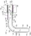
图1是根据示例性实施例的电气装置的侧视平面图。FIG. 1 is a side plan view of an electrical device according to an exemplary embodiment.
图2是根据示例性实施例的电气装置的侧视平面图。2 is a side plan view of an electrical device according to an exemplary embodiment.
图3是根据示例性实施例的电气装置的侧视平面图。3 is a side plan view of an electrical device according to an exemplary embodiment.
图4是根据示例性实施例的电气装置的透视图。4 is a perspective view of an electrical device according to an exemplary embodiment.
图5是根据示例性实施例的电气装置的透视图。5 is a perspective view of an electrical device according to an exemplary embodiment.
具体实施方式Detailed ways
本文阐述的实施例可以包括配置为用于通信数据信号的各种电连接器。电连接器可以与对应的配合连接器配合,以通信地互连通信系统的不同部件。在所示的实施例中,电连接器是插头连接器,其可以端接至并电联接至另一电气部件,例如电路板、线束或另一电气部件。插头连接器可以是可插拔的输入/输出(I/O)连接器,其在配合操作期间可以与对应的插座连接器配合。然而,应当理解,本文阐述的创造性主题可以适用于其他类型的电连接器。The embodiments set forth herein may include various electrical connectors configured for communicating data signals. The electrical connectors can mate with corresponding mating connectors to communicatively interconnect different components of the communication system. In the illustrated embodiment, the electrical connector is a plug connector that can be terminated to and electrically coupled to another electrical component, such as a circuit board, a wire harness, or another electrical component. The plug connector may be a pluggable input/output (I/O) connector that mates with a corresponding receptacle connector during a mating operation. It should be understood, however, that the inventive subject matter set forth herein may be applicable to other types of electrical connectors.
在各种实施例中,电连接器提供柔性电路板,在每个实施例中,柔性电路板上下叠置以形成电连接器。每个实施例包括刚性部分和柔性部分,并且在至少一个实施例中,刚性部分包括刚性印刷电路板(PCB),在至少一个实施例中,刚性部分仅包括柔性基板,例如柔性PCB,也称为可弯曲PCB。为了本公开的目的,柔性装置配置为遵循期望的形状,包括通过围绕半径弯曲。在一个示例中,柔性PCB能够弯曲至少四十五(45)度而不会断裂。为了本公开的目的,刚性装置配置为保持相同的形状并且不围绕半径弯曲。在一个示例中,刚性PCB在不会断裂的情况下不能弯曲至多十五(15)度。在一个这样的实施例中,柔性基板的四个层上下叠置,第一和第二柔性基板延伸经过第三和第四柔性基板的端部,以形成四个柔性基板刚性部分和两个柔性基板柔性部分。通过在实施例中利用柔性部分,电缆可以彼此交错或偏移以改善串扰,同时柔性部分保持期望的空间要求,包括通过减小高度和形成直角插头。因此,除了增加性能外,还减少了原电缆上的压力,从而延长了系统寿命。In various embodiments, the electrical connector provides a flexible circuit board which, in each embodiment, is stacked on top of one another to form the electrical connector. Each embodiment includes a rigid portion and a flexible portion, and in at least one embodiment, the rigid portion includes a rigid printed circuit board (PCB), and in at least one embodiment, the rigid portion includes only a flexible substrate, such as a flexible PCB, also known as For bendable PCB. For the purposes of this disclosure, a flexible device is configured to follow a desired shape, including by bending around a radius. In one example, the flexible PCB is capable of bending at least forty-five (45) degrees without breaking. For the purposes of this disclosure, the rigid device is configured to maintain the same shape and not bend around a radius. In one example, a rigid PCB cannot bend up to fifteen (15) degrees without breaking. In one such embodiment, four layers of flexible substrates are stacked on top of each other, with the first and second flexible substrates extending past the ends of the third and fourth flexible substrates to form four flexible substrate rigid portions and two flexible substrates The flexible part of the substrate. By utilizing flexible portions in embodiments, the cables can be staggered or offset from each other to improve crosstalk, while the flexible portions maintain desired space requirements, including by reducing height and forming right-angle plugs. Thus, in addition to increased performance, stress on the original cable is reduced, thereby extending system life.
图1和图2示出了处于第一位置(图1)和第二位置(图2)中的示例性电气装置100的侧视平面图。在一个示例性实施例中,电气装置100是直接附接连接器。电气装置100包括第一柔性基板102、第二柔性基板104、设置在第一柔性基板102和第二柔性基板104之间的刚性基板106、第一组电缆107、第二组电缆108、第一电介质保持器114和第二电介质保持器116。1 and 2 illustrate side plan views of the exemplary
第一柔性基板102从第一配合端118延伸到第一端接端120。在一个示例实施例中,第一柔性基板102是柔性印刷电路板(PCB)。在第一配合端118和第一端接端120之间,第一柔性基板102在第一位置(图1)至第二位置(图2)之间弯曲或挠曲。在一个示例中,当电气装置100处于第二位置(图2)时,电气装置100是直角插头。因此,第一柔性基板102包含包括配合端118的配合部分122、弧形部分124以及包括端接端120的端接部分126。当由柔性基板材料形成时,在一个实施例中,配合部分122和端接部分126都保持大致上笔直,而弧形部分124在第一位置(图1)保持笔直并在第二位置(图2)弯曲或具有弧形。The first
第二柔性基板104相对于第一柔性基板102间隔开平行地延伸。类似于第一柔性基板102,第二柔性基板104从第二配合端128延伸到第二端接端130。在第二配合端128和第二端接端130之间,第二柔性基板104从第一位置(图1)弯曲或挠曲到第二位置(图2)。在一个示例中,当电气装置100处于第二位置(图2)时,电气装置100是直角插头。因此,第二柔性基板104包含包括配合端128的配合部分132、弧形部分134以及包括端接端130的端接部分136。当由柔性基板材料形成时,在一个实施例中,配合部分132和端接部分136都保持大致上笔直,而弧形部分134在第一位置(图1)保持笔直并在第二位置(图2)弯曲或具有弧形。The second
刚性基板106在第一柔性基板102的第一配合端118和第二柔性基板104的第二配合端128附近联接到第一柔性基板102和第二柔性基板104且在它们之间延伸,以在第一柔性基板102和第二柔性基板104之间提供电连接。刚性基板106从配合边缘106A延伸到端接边缘106B。以这种方式,第一柔性基板102、第二柔性基板104、端接边缘106B(并且在该示例实施例中是刚性第一电介质保持器114的边缘129)限定了开放空腔127。替代地,(如图3-4的示例性实施例所示),空腔仅由刚性基板的端接边缘和间隔开的柔性电路板限定。以这种方式,空腔127允许第一柔性基板102和第二柔性基板104弯曲,如图2所示。尽管在此示例中,刚性基板106设置在第一柔性基板102和第二柔性基板104之间并提供第一柔性基板102和第二柔性基板104之间的连接,但在其他示例(图5)中,分层的柔性基板形成电气装置100刚性部分且没有使用刚性基板。在每个示例实施例中,配合端因此是刚性的,并且配置为插接到配合电连接器(未示出)中。另外,在该示例实施例中,空腔是开放的,在其中提供空气;但是,替代地,也可以将诸如泡沫的柔性物质设置在空腔内或填充空腔,以提供绝缘、增强导电性、提高耐用性、增加鲁棒性等。The
在一个示例中,第一组电缆107包括设置在电缆护套139内的多个信号导体137,以及在信号导体137周围延伸并围绕其的第一接地信号导体138。另外,多个信号导体137以并排布置放置以形成第一层140。第一层140内并排的多个双信号导体137被多个对应的信号触头142接收,使得每个信号导体137被对应的信号触头142接收。在示例实施例中,信号触头142可以是在第一柔性基板102上的垫、镀覆通孔等。在一个实施例中,每个信号导体137是中继信号的通信电缆,其中沿着这样的电缆的EMI和干扰导致串扰。In one example, the first set of
类似地,在一个示例中,第二组电缆108包括设置在电缆护套139内的多个双信号导体137,以及在双信号导体137周围延伸并围绕其的第二接地信号导体143。另外,多个双信号导体137以并排布置放置以形成第二层144。第二层144内并排的多个双信号导体137被多个对应的信号触头142接收,使得每个信号导体137被对应的信号触头142接收。在示例实施例中,信号触头142可以是在第二柔性基板104上的垫、镀覆通孔等。在一个实施例中,每个信号导体137是中继信号的通信电缆,其中沿着这样的电缆的EMI和干扰导致串扰。Similarly, in one example, the second set of
第一电介质保持器114分别将第一组电缆107和第二组电缆108固定到第一柔性基板102和第二柔性基板104。第一电介质保持器114可以是粘合剂,热熔体等。同时,第二电介质保持器116将第一层140中的多个并排的电缆护套139彼此固定,并且将第二层144中的多个并排的电缆护套139彼此固定。第二电介质保持器116还将第一组电缆107和第二组电缆108固定到第一柔性基板102的第一端接端120和第二柔性基板104的第二端接端130。第二电介质保持器116可以是粘合剂,热熔体等。尽管被描述为第一电介质保持器114和第二电介质保持器116,但是在示例实施例中,第一电介质保持器114和第二电介质保持器116是一件式构造的。The
总体而言,电气装置100提供了一种连接器,该连接器能够在端接端和配合端之间挠曲或弯曲以减小电气装置100的高度。另外,电气装置100的柔性减小了连接到电气装置的原电缆上的应力。尽管在该示例实施例中使用第一柔性基板102和第二柔性基板104,替代地,可以使用两个柔性基板表面,从而提供单个柔性基板。在一个示例中,两个独立的柔性基板被接合或联接。替代地,提供单个基板,该基板具有在公共基部处联接或接合的两个机械独立的部分。因此,可以使用单个柔性基板。In general, the
图3和图4示出了示例性电气装置300。在一个示例性实施例中,电气装置300是直接附接连接器。在该示例性实施例中,电气装置300包括第一柔性基板302、第二柔性基板304、从第一柔性基板302延伸的第三柔性基板305、设置在第一柔性基板302和第二柔性基板304之间的具有配合边缘306A和端接端306B的刚性基板306。电气装置还包括联接到第一柔性基板302的第一组电缆307、联接到第二柔性基板304的第二组电缆308、联接到第三柔性基板305的第三组电缆310、第一电介质保持器314、第二电介质保持器316和第三电介质保持器317。An example
第一柔性基板302从第一配合端318延伸到第一端接端320。在一个示例中,类似于图1-2所示的示例性实施例,在第一配合端318和第一端接端320之间,第一柔性基板302从第一位置弯曲到第二位置。在一个示例中,当电气装置300处于第二位置时,电气装置300是直角插头。The first
第二柔性基板304相对于第一柔性基板302间隔开平行地延伸。类似于第一柔性基板302,第二柔性基板304从第二配合端328延伸到第二端接端330。在一个示例中,类似于图1-2所示的示例性实施例,第二配合端328和第二端接端330之间,第二柔性基板304的从第一位置弯曲到第二位置。The second
第三柔性基板305从第三配合端332处的第一柔性基板302延伸到第三端接端334。第三配合端332从第一柔性基板302延伸,使得第三配合端332从第一柔性基板302的第一配合端318纵向偏移,且从第二柔性基板304的第二配合端328纵向偏移。第三柔性基板305包括对角部分336,其从第三配合端332对角地延伸到线性部分338,该线性部分338从对角部分延伸到第三端接端334。线性部分338相对于第一柔性基板302和第二柔性基板304平行且垂直间隔开地延伸。The third
刚性基板306在第一柔性基板302的第一配合端318和第二柔性基板304的第二配合端328附近联接到第一柔性基板302和第二柔性基板304且在它们之间延伸,以在第一柔性基板302和第二柔性基板304之间提供电连接。刚性基板306从配合边缘306A延伸到端接边缘306B。以这种方式,第一柔性基板302、第二柔性基板304和端接边缘306B限定开放空腔127。以这种方式,空腔327允许第一柔性基板302和第二柔性基板304弯曲。另外,在该示例实施例中,空腔是开放的,在其中提供空气;但是,替代地,也可以将诸如泡沫的柔性物质设置在空腔内或填充空腔,以提供绝缘、增强导电性、提高耐用性、增加鲁棒性等。The
在一个示例中,第一组电缆307包括设置在电缆护套344内的多个信号导体342,以及在双信号导体342周围延伸并围绕其的第一接地信号导体343。另外,多个双信号导体342以并排布置放置以形成第一层346。第一层346内并排的多个双信号导体342被多个对应的信号触头348接收,使得每个信号导体342被对应的信号触头348接收。在示例实施例中,信号触头348可以是在第一柔性基板302上的垫、镀覆通孔等。在一个实施例中,每个信号导体342是中继信号的通信电缆,其中沿着这样的电缆的EMI和干扰导致串扰。In one example, the first set of
类似地,在一个示例中,第二组电缆308包括设置在电缆护套344内的多个双信号导体342,以及在双信号导体342周围延伸并围绕其的第二接地信号导体350。另外,多个双信号导体342以并排布置放置以形成第二层352。第二层352内并排的多个双信号导体342被多个对应的信号触头354接收,使得每个信号导体342被对应的信号触头354接收。在示例实施例中,信号触头354可以是在第二柔性基板304上的垫、镀覆通孔等。在一个实施例中,每个信号导体342是中继信号的通信电缆,其中沿着这样的电缆的EMI和干扰导致串扰。具体地,在示例实施例中,第二组电缆308具有比第一组电缆306更少的双信号导体342。以这种方式,第一柔性基板302的信号导体342直接上下叠置并且彼此纵向对准,但是第一柔性基板302的信号导体342与第二柔性基板304的信号导体342横向偏移。以这种方式,第一柔性基板302的信号导体342与第二柔性基板304的信号导体342交错,从而减少串扰的影响并改善信号质量。Similarly, in one example, the second set of
类似地,在一个示例中,第三组电缆310包括多个信号导体342,以及设置在电缆护套344内的第三接地信号导体356,电缆护套344在信号导体342周围延伸并围绕信号导体342。另外,多个信号导体342以并排布置放置以形成第三层358。第三层358内并排的多个信号导体342被多个对应的信号触头354接收,使得每个信号导体342被对应的信号触头360接收。在示例实施例中,信号触头360可以是在第三柔性基板305上的垫、镀覆通孔等。在一个实施例中,每个信号导体342是中继信号的通信电缆,其中沿着这样的电缆的EMI和干扰导致串扰。具体地,在示例实施例中,第二组电缆308具有比第一组电缆306和第二组电缆308更少的信号导体342。以这种方式,第一柔性基板302的信号导体342和第二柔性基板304的信号导体342都直接位于第三柔性基板305的信号导体342的上方并与它们纵向对准。同时,第二柔性基板304的导体342与第三柔性基板305的信号导体342横向地偏移。再次,以这种方式,第二柔性基板304的信号导体342与第三柔性基板305的信号导体342交错,从而减少串扰的影响并改善信号质量。Similarly, in one example, the third set of
第一电介质保持器314分别将第一组电缆307和第三组电缆309固定到第一柔性基板302和第三柔性基板305。在示例实施例中,第一电介质保持器314是一件式构造,并且是粘合剂或热熔体。替代地,在另一实施例中,第一电介质保持器314以两个分开的部分施加,一个部分将第一组电缆307固定到第一柔性基板302,另一个部分将第三组电缆309固定到第三柔性基板305。同时,第二电介质保持器316将第二组电缆308固定到第二柔性基板304,而第三电介质保持器317将第二层352中的多个并排的电缆护套344彼此固定。尽管在该示例性实施例中,第二电介质保持器316和第三电介质保持器317设置为单独的部分,但是在另一个实施例中,这些部分是类似于相对于第一层346和第三层358的第一电介质保持器314的一件式构造。在示例实施例中,每个电介质保持器314、316和317是粘合剂或热熔体。The
因此,提供了具有交错的多组电缆306、308、309以减少串扰的柔性和刚性的电气装置300布置。另外,这种布置允许使用较小规格的电缆,从而减少了电缆的端接端的串扰耦合。因此,走线损失也被最小化。Thus, a flexible and rigid
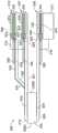
图5示出了另一个示例性电气装置500的透视图,该电气装置500具有刚性和柔性布置。在一个示例性实施例中,电气装置500是直接附接连接器。在该示例性实施例中,电气装置500包括第一柔性基板502、第二柔性基板504、第三柔性基板506、第四柔性基板508、联接到第一柔性基板502的第一组电缆510、联接到第二柔性基板504的第二组电缆512和联接到第三柔性基板506的第三组电缆514。虽然可以使用电介质保持器材料的部分来固定电缆组510、512和514,但是在该实施例中,未示出电介质保持器材料。FIG. 5 shows a perspective view of another exemplary
在电气装置500的该实施例中,柔性基板502、504、506和508上下叠置以形成刚性部分516和柔性部分518。刚性部分516包括柔性基板502、504、506和508中的每一个,或者具有四层布置。因为刚性部分516包括四个层,这些层一起抵抗弯曲,使它们的功能类似于刚性基板。以这种方式,柔性基板可以用于形成刚性系统,从而减少了制造电气装置500所需的不同零件的数量。柔性部分518仅包括第二柔性基板504和第三柔性基板506,它们各自延伸经过第一柔性基板502和第四柔性基板508以提供两层布置。如图所示,类似于先前的实施例,由于基板504、506之间的联接(未示出)而在第二柔性基板504和506之间形成空腔519,以促进柔性部分518的弯曲。可选地,可以在第二柔性基板504和506之间放置柔性基板、泡沫等以改善装置特性,但是仍然提供柔性。以这种方式,双柔性基板504和506以关于图1-2的第一柔性基板102和第二柔性基板104所描述的方式弯曲。In this embodiment of
第一柔性基板502从配合端520延伸到端接端522,并且在端接端522处还包括多个信号触头524,用于接收第一组电缆510。第二柔性基板504联接到第一柔性基板502。第二柔性基板504类似地从配合端526延伸到端接端528,并且在端接端528处包括多个信号触头(未示出),用于接收第二组电缆512。The first
第三柔性基板506联接到第一柔性基板502,并且也从配合端530延伸到端接端532,并且在端接端532处包括多个信号触头534,用于接收第三组电缆514。第三柔性基板506不延伸第一柔性基板502的整个长度。而是,第一柔性基板502延伸经过第三柔性基板的端接端532到第一柔性基板502的端接端522。The third
第四柔性基板508联接到第二柔性基板504且相对于第三柔性基板506间隔开,使得第一柔性基板502和第二柔性基板504对准或夹在第一柔性基板502和第二柔性基板504之间。第四柔性基板508从配合端536延伸到端接端538,并且包括多个信号触头(未示出),用于接收第四组电缆(未示出)。类似于第三柔性基板,第四柔性基板508不延伸第二柔性基板504的整个长度。而是,第二柔性基板504延伸经过第四柔性基板508的端接端538到第二柔性基板504的端接端528。以这种方式,即使每个基板分别是柔性的,第一柔性基板502、第二柔性基板504、第三柔性基板506和第四柔性基板508也上下叠置以形成刚性部分516。同时,第一柔性基板502和第二柔性部分504的延伸经过第三柔性基板506和第四柔性基板508的部分分别形成柔性部分518,因为只有两个柔性基板(第一柔性基板502和第二柔性基板504)能够一起弯曲或挠曲,类似于之前描述的实施例。因此,在制造期间,不需要刚性面板,从而降低制造复杂性。另外,这种布置还允许电缆组在水平或竖直地相互偏移,从而减少了电气装置500中的串扰和干扰。The fourth
在一个示例中,第一组电缆510包括多个信号导体540,以及设置在电缆护套544内的第一接地信号导体542,电缆护套344在信号导体540周围延伸并围绕信号导体342。第一组电缆510的每个电缆护套544从第一柔性基板502附近并在第二柔性基板504上延伸。另外,多个双信号导体540以并排布置放置以形成双信号导体540的第一层546。第一层546内并排的多个双信号导体540被多个对应的信号触头524接收,使得每个信号导体540被对应的信号触头524接收。在示例实施例中,信号触头524可以是在第一柔性基板502上的垫、镀覆通孔等。在一个实施例中,每个信号导体540是中继信号的通信电缆,其中沿着这样的电缆的EMI和干扰导致串扰。In one example, the first set of
在一个示例中,第二组电缆512包括多个信号导体540,以及设置在电缆护套544内的第二接地信号导体(未示出),电缆护套344在信号导体540周围延伸并围绕信号导体342。第二组电缆512的每个电缆护套544从第二柔性基板504附近并远离第二柔性基板504延伸。另外,多个双信号导体540以并排布置放置以形成双信号导体540的第二层552。第二层552内并排的多个双信号导体540被多个对应的信号触头(未示出)接收,使得每个信号导体540被对应的信号触头(未示出)接收。在示例实施例中,信号触头可以是在第二柔性基板504上的垫、镀覆通孔等。在一个实施例中,每个信号导体540是中继信号的通信电缆,其中沿着这样的电缆的EMI和干扰导致串扰。In one example, the second set of
在一个示例中,第三组电缆514包括多个信号导体540,以及设置在电缆护套544内的第三接地信号导体554,电缆护套344在信号导体540周围延伸并围绕信号导体342。第三组电缆514的每个电缆护套544从第三柔性基板506附近并远离第三柔性基板506延伸。另外,多个双信号导体540以并排布置放置以形成双信号导体540的第三层556。第三层556内并排的多个双信号导体540被多个对应的信号触头534接收,使得每个信号导体540被对应的信号触头534接收。在示例实施例中,信号触头534可以是在第三柔性基板506上的垫、镀覆通孔等。在一个实施例中,每个信号导体540是中继信号的通信电缆,其中沿着这样的电缆的EMI和干扰导致串扰。在一个实施例中,第二柔性基板504和第三柔性基板506的信号导体540被布置成偏移或交错的,包括类似于图3-4的示例性实施例中所示的布置。以这种方式,高密度电子装置500具有减小的串扰,同时还改善了电子装置500的高度。In one example, the third set of
Claims (11)
Applications Claiming Priority (2)
| Application Number | Priority Date | Filing Date | Title |
|---|---|---|---|
| US16/250,442US11095075B2 (en) | 2019-01-17 | 2019-01-17 | Electrical device with a plug connector having a flexible section |
| US16/250,442 | 2019-01-17 |
Publications (2)
| Publication Number | Publication Date |
|---|---|
| CN111463600Atrue CN111463600A (en) | 2020-07-28 |
| CN111463600B CN111463600B (en) | 2024-09-10 |
Family
ID=71610144
Family Applications (1)
| Application Number | Title | Priority Date | Filing Date |
|---|---|---|---|
| CN202010051374.1AActiveCN111463600B (en) | 2019-01-17 | 2020-01-17 | Electrical device having plug connector with flexible portion |
Country Status (2)
| Country | Link |
|---|---|
| US (1) | US11095075B2 (en) |
| CN (1) | CN111463600B (en) |
Cited By (1)
| Publication number | Priority date | Publication date | Assignee | Title |
|---|---|---|---|---|
| US12185456B2 (en) | 2021-12-09 | 2024-12-31 | First Hi-Tec Enterprise Co., Ltd. | Circuit board with rigid portion and flexible portion having connecting end and electronic package using the same |
Citations (23)
| Publication number | Priority date | Publication date | Assignee | Title |
|---|---|---|---|---|
| EP0147566A2 (en)* | 1984-01-03 | 1985-07-10 | International Business Machines Corporation | Method of forming contacts for flexible module carriers |
| JPH0850971A (en)* | 1994-08-05 | 1996-02-20 | Oki Densen Kk | Relay connector for orthogonal type flexible substrate and rigid substrate |
| US6126459A (en)* | 1997-03-24 | 2000-10-03 | Ford Motor Company | Substrate and electrical connector assembly |
| US20050190006A1 (en)* | 2004-02-27 | 2005-09-01 | Atsuhito Noda | Flat flexible circuitry |
| US20050276547A1 (en)* | 2004-06-14 | 2005-12-15 | Wang Charles X | Fiber optic transceiver module with rigid and flexible circuit boards |
| CN1728464A (en)* | 2004-07-28 | 2006-02-01 | 第一电子工业株式会社 | Connector |
| US20060148282A1 (en)* | 2004-12-30 | 2006-07-06 | Nokia Corporation | Electronic component assembly |
| CN1819346A (en)* | 2005-01-26 | 2006-08-16 | 欧姆龙株式会社 | Connector |
| US20070032104A1 (en)* | 2005-08-08 | 2007-02-08 | Ddk Ltd. | Electrical connector |
| CN1939104A (en)* | 2004-04-09 | 2007-03-28 | 大日本印刷株式会社 | Rigid-flex board and method of manufacturing the same |
| CN101031185A (en)* | 2006-02-27 | 2007-09-05 | 株式会社藤仓 | Connection configuration for rigid substrates |
| US7544066B1 (en)* | 2008-03-10 | 2009-06-09 | Apple Inc. | Electrical connector with flexible interconnect |
| JP2010062350A (en)* | 2008-09-04 | 2010-03-18 | Sumitomo Electric Ind Ltd | Connector circuit board and method for manufacturing the same |
| CN101971428A (en)* | 2008-03-11 | 2011-02-09 | 住友电木株式会社 | Connector unit and electronics |
| CN102709755A (en)* | 2010-07-19 | 2012-10-03 | 泰科电子公司 | Transceiver assembly |
| CN102714383A (en)* | 2010-03-01 | 2012-10-03 | 株式会社藤仓 | Connector assembly |
| US20140206230A1 (en)* | 2013-01-18 | 2014-07-24 | Molex Incorporated | Paddle Card Assembly For High Speed Applications |
| US9590338B1 (en)* | 2015-11-30 | 2017-03-07 | Te Connectivity Corporation | Rigid-flex circuit connector |
| US20170093059A1 (en)* | 2015-09-25 | 2017-03-30 | Kuan-Yu Chen | Connection structures for providing a reference potential to a flexible circuit device |
| US20170172007A1 (en)* | 2015-12-09 | 2017-06-15 | Mellanox Technologies Ltd. | Multi-slot plug-in card |
| US20170194721A1 (en)* | 2016-01-06 | 2017-07-06 | Chih-Peng Fan | Electrical Connector and Method of Making It |
| US10050361B1 (en)* | 2017-05-22 | 2018-08-14 | Te Connectivity Corporation | Flexible circuit connector |
| CN108780958A (en)* | 2016-03-15 | 2018-11-09 | 3M创新有限公司 | Rotary connector component |
Family Cites Families (3)
| Publication number | Priority date | Publication date | Assignee | Title |
|---|---|---|---|---|
| US5710393A (en) | 1995-05-17 | 1998-01-20 | The Whitaker Corporation | Modular array termination for multiconductor electrical cables |
| US6055722A (en) | 1998-05-20 | 2000-05-02 | Trw Inc. | Stripline flexible cable to printed circuit board attachment system |
| US8292655B1 (en) | 2011-04-01 | 2012-10-23 | Intel Corporation | Innovative cable termination scheme |
- 2019
- 2019-01-17USUS16/250,442patent/US11095075B2/enactiveActive
- 2020
- 2020-01-17CNCN202010051374.1Apatent/CN111463600B/enactiveActive
Patent Citations (27)
| Publication number | Priority date | Publication date | Assignee | Title |
|---|---|---|---|---|
| EP0147566A2 (en)* | 1984-01-03 | 1985-07-10 | International Business Machines Corporation | Method of forming contacts for flexible module carriers |
| JPH0850971A (en)* | 1994-08-05 | 1996-02-20 | Oki Densen Kk | Relay connector for orthogonal type flexible substrate and rigid substrate |
| US6126459A (en)* | 1997-03-24 | 2000-10-03 | Ford Motor Company | Substrate and electrical connector assembly |
| US20050190006A1 (en)* | 2004-02-27 | 2005-09-01 | Atsuhito Noda | Flat flexible circuitry |
| CN1939104A (en)* | 2004-04-09 | 2007-03-28 | 大日本印刷株式会社 | Rigid-flex board and method of manufacturing the same |
| US20050276547A1 (en)* | 2004-06-14 | 2005-12-15 | Wang Charles X | Fiber optic transceiver module with rigid and flexible circuit boards |
| CN1728464A (en)* | 2004-07-28 | 2006-02-01 | 第一电子工业株式会社 | Connector |
| US20060148282A1 (en)* | 2004-12-30 | 2006-07-06 | Nokia Corporation | Electronic component assembly |
| CN1819346A (en)* | 2005-01-26 | 2006-08-16 | 欧姆龙株式会社 | Connector |
| US20070032104A1 (en)* | 2005-08-08 | 2007-02-08 | Ddk Ltd. | Electrical connector |
| CN101031185A (en)* | 2006-02-27 | 2007-09-05 | 株式会社藤仓 | Connection configuration for rigid substrates |
| US7544066B1 (en)* | 2008-03-10 | 2009-06-09 | Apple Inc. | Electrical connector with flexible interconnect |
| CN101971428A (en)* | 2008-03-11 | 2011-02-09 | 住友电木株式会社 | Connector unit and electronics |
| JP2010062350A (en)* | 2008-09-04 | 2010-03-18 | Sumitomo Electric Ind Ltd | Connector circuit board and method for manufacturing the same |
| CN102714383A (en)* | 2010-03-01 | 2012-10-03 | 株式会社藤仓 | Connector assembly |
| US20120322278A1 (en)* | 2010-03-01 | 2012-12-20 | Fujikura Ltd. | Connector assembly |
| US8753144B2 (en)* | 2010-03-01 | 2014-06-17 | Fujikura Ltd. | Connector assembly having insulating material with different dielectric constant |
| CN102709755A (en)* | 2010-07-19 | 2012-10-03 | 泰科电子公司 | Transceiver assembly |
| US20140206230A1 (en)* | 2013-01-18 | 2014-07-24 | Molex Incorporated | Paddle Card Assembly For High Speed Applications |
| US20170093059A1 (en)* | 2015-09-25 | 2017-03-30 | Kuan-Yu Chen | Connection structures for providing a reference potential to a flexible circuit device |
| US9590338B1 (en)* | 2015-11-30 | 2017-03-07 | Te Connectivity Corporation | Rigid-flex circuit connector |
| CN106921060A (en)* | 2015-11-30 | 2017-07-04 | 泰科电子公司 | Rigid flex-circuits connector |
| US20170172007A1 (en)* | 2015-12-09 | 2017-06-15 | Mellanox Technologies Ltd. | Multi-slot plug-in card |
| US20170194721A1 (en)* | 2016-01-06 | 2017-07-06 | Chih-Peng Fan | Electrical Connector and Method of Making It |
| CN108780958A (en)* | 2016-03-15 | 2018-11-09 | 3M创新有限公司 | Rotary connector component |
| US10050361B1 (en)* | 2017-05-22 | 2018-08-14 | Te Connectivity Corporation | Flexible circuit connector |
| CN108933361A (en)* | 2017-05-22 | 2018-12-04 | 泰连公司 | Flexible circuit connector |
Non-Patent Citations (1)
| Title |
|---|
| 杨建生: "芯片上芯片(COC)与板上芯片(COB)组装技术-挠曲刚性印制电路组装", 半导体行业, no. 003, 31 December 2007 (2007-12-31)* |
Cited By (1)
| Publication number | Priority date | Publication date | Assignee | Title |
|---|---|---|---|---|
| US12185456B2 (en) | 2021-12-09 | 2024-12-31 | First Hi-Tec Enterprise Co., Ltd. | Circuit board with rigid portion and flexible portion having connecting end and electronic package using the same |
Also Published As
| Publication number | Publication date |
|---|---|
| US20200235525A1 (en) | 2020-07-23 |
| US11095075B2 (en) | 2021-08-17 |
| CN111463600B (en) | 2024-09-10 |
Similar Documents
| Publication | Publication Date | Title |
|---|---|---|
| CN109616810B (en) | A kind of interface unit | |
| JP6703900B2 (en) | Connectors and connector systems | |
| US11637400B2 (en) | Electrical cable connector | |
| US9281632B2 (en) | Communication jack having layered plug interface contacts | |
| US11289854B2 (en) | Electrical connecting device | |
| CN103996933B (en) | The method for transmitting signals of connector and this connector of use | |
| US20150111402A1 (en) | Electrical device having a circuit board and a differential pair of signal conductors terminated thereto | |
| CN103378495A (en) | Electrical connector and wire assembly | |
| CN106356688B (en) | Construct pluggable connectors and interconnection systems for resonance control | |
| TWI750848B (en) | Connecting object, connector and harness | |
| TWI794231B (en) | Electrical device having an insulator wafer | |
| TWI761991B (en) | Connector assembly | |
| US9905972B2 (en) | Plug connector having crosstalk compensation | |
| US11165208B2 (en) | Electrical contact and connector | |
| WO2006060726A1 (en) | Board-to-board connector | |
| US6695646B1 (en) | Electrical connector having floatable chicklets | |
| CN116547872A (en) | High-speed hermaphrodite connectors and connector assemblies | |
| CN1229292A (en) | Right Angle Electrical Connector | |
| CN111463600B (en) | Electrical device having plug connector with flexible portion | |
| JP7671357B2 (en) | Cable connectors and electronic devices | |
| JP2008004368A (en) | Connector | |
| CN209824120U (en) | Circuit board and electric connector with same | |
| JP2011018621A (en) | Connector component and connector | |
| CN101944671B (en) | Circuit cable with plug-in positioning structure | |
| CN102005668B (en) | Circuit board plug positioning connector |
Legal Events
| Date | Code | Title | Description |
|---|---|---|---|
| PB01 | Publication | ||
| PB01 | Publication | ||
| SE01 | Entry into force of request for substantive examination | ||
| SE01 | Entry into force of request for substantive examination | ||
| GR01 | Patent grant | ||
| GR01 | Patent grant | ||
| TR01 | Transfer of patent right | ||
| TR01 | Transfer of patent right | Effective date of registration:20250710 Address after:Schaffhausen Patentee after:Tailian Service Co.,Ltd. Country or region after:Switzerland Address before:Pennsylvania, USA Patentee before:TE CONNECTIVITY Corp. Country or region before:U.S.A. | |
| TR01 | Transfer of patent right | ||
| TR01 | Transfer of patent right | Effective date of registration:20250903 Address after:Schaffhausen Patentee after:Tailian solutions Co.,Ltd. Country or region after:Switzerland Address before:Schaffhausen Patentee before:Tailian Service Co.,Ltd. Country or region before:Switzerland |