CN111459543B - Method for managing register file unit - Google Patents
Method for managing register file unitDownload PDFInfo
- Publication number
- CN111459543B CN111459543BCN201910052633.XACN201910052633ACN111459543BCN 111459543 BCN111459543 BCN 111459543BCN 201910052633 ACN201910052633 ACN 201910052633ACN 111459543 BCN111459543 BCN 111459543B
- Authority
- CN
- China
- Prior art keywords
- register
- thread
- sub
- register file
- groups
- Prior art date
- Legal status (The legal status is an assumption and is not a legal conclusion. Google has not performed a legal analysis and makes no representation as to the accuracy of the status listed.)
- Active
Links
Images


Classifications
- G—PHYSICS
- G06—COMPUTING OR CALCULATING; COUNTING
- G06F—ELECTRIC DIGITAL DATA PROCESSING
- G06F9/00—Arrangements for program control, e.g. control units
- G06F9/06—Arrangements for program control, e.g. control units using stored programs, i.e. using an internal store of processing equipment to receive or retain programs
- G06F9/30—Arrangements for executing machine instructions, e.g. instruction decode
- G06F9/30098—Register arrangements
- G06F9/30141—Implementation provisions of register files, e.g. ports
Landscapes
- Engineering & Computer Science (AREA)
- Software Systems (AREA)
- Theoretical Computer Science (AREA)
- Physics & Mathematics (AREA)
- General Engineering & Computer Science (AREA)
- General Physics & Mathematics (AREA)
- Executing Machine-Instructions (AREA)
Abstract
Translated fromChinese
Description
Translated fromChinese技术领域technical field
本发明涉及处理器设计领域,尤其涉及一种管理寄存器文件单元的方法。The invention relates to the field of processor design, in particular to a method for managing register file units.
背景技术Background technique
寄存器文件单元(Register File)又称寄存器堆,是CPU或GPU等处理器中由多个寄存器组成的阵列,可由触发器或静态随机存取存储器(SRAM)实现。The register file unit (Register File), also known as the register file, is an array composed of multiple registers in processors such as CPU or GPU, which can be realized by flip-flops or static random access memory (SRAM).
通用计算图形处理器(General-Purpose Graphic Processing Unit,GPGPU)是一种大规模并行处理器,已成功应用于具有显著线程并行性的高性能计算领域,每个时钟周期能够同时处理多个线程。在这种并行处理中,每个线程独立处理不同的数据集,这些数据及中间运算结果均需要暂存到片上寄存器文件单元。由于支持的线程数较多并且每个线程需要的寄存器数量也较多,GPGPU采用静态随机存取存储器(SRAM)而非触发器来实现寄存器文件单元以减小面积与降低功耗。这种SRAM具有专门的读端口与写端口,可以多路并发访问不同的寄存器。General-Purpose Graphic Processing Unit (GPGPU) is a massively parallel processor that has been successfully applied in the field of high-performance computing with significant thread parallelism, capable of processing multiple threads simultaneously per clock cycle. In this parallel processing, each thread independently processes different data sets, and these data and intermediate operation results need to be temporarily stored in the on-chip register file unit. Due to the number of supported threads and the number of registers required for each thread, GPGPU uses static random access memory (SRAM) instead of flip-flops to implement register file units to reduce area and power consumption. This SRAM has a dedicated read port and write port, which can access different registers concurrently in multiple ways.
GPGPU通过执行程序指令来实现特定的功能,以标量指令而言,其最多读取三个源操作数进行计算并写回一个目的操作数,例如,乘累加指令,因此SRAM需要三个读端口和一个写端口,但三读一写的SRAM需要专门的定制设计,费时且昂贵。GPGPU implements specific functions by executing program instructions. In terms of scalar instructions, it reads up to three source operands for calculation and writes back one destination operand, such as multiply-accumulate instructions, so SRAM requires three read ports and One write port, but a three-read-one-write SRAM requires a specialized custom design, which is time-consuming and expensive.
由于标量访存指令每次访存仅能读取一个32位数据,为提高访存效率,提出一种一次访存操作读取四个32位数据的向量访存指令,在这种方式下,如果需单周期完成写回操作,则四个32位数据需SRAM包含四个写端口,加上上文所述的三个读端口,总计需要三个读端口与四个写端口。这种多端口的SRAM设计,其实现成本与复杂度将难以承受,而如果采用多个周期完成写回操作的方式,则会带来性能的损失。Since the scalar memory access instruction can only read one 32-bit data per memory access, in order to improve the memory access efficiency, a vector memory access instruction that reads four 32-bit data in one memory access operation is proposed. In this way, If the write-back operation needs to be completed in a single cycle, four 32-bit data SRAMs need to contain four write ports, plus the three read ports described above, a total of three read ports and four write ports are required. The implementation cost and complexity of this multi-port SRAM design will be unbearable, and if multiple cycles are used to complete the write-back operation, performance will be lost.
因此,需要对现有技术进行改进,以利用单端口存储器模拟多端口存储器,从而降低寄存器文件单元的设计成本并提高访存性能。Therefore, there is a need to improve the prior art to emulate a multi-port memory with a single-port memory, thereby reducing the design cost of the register file unit and improving the memory access performance.
发明内容SUMMARY OF THE INVENTION
本发明的目的在于克服上述现有技术的缺陷,提供一种管理寄存器文件单元的方法。The purpose of the present invention is to overcome the above-mentioned defects of the prior art, and to provide a method for managing register file units.
根据本发明的第一方面,提供了一种管理寄存器文件单元的方法,所述寄存器文件单元由单端口存储器构成,所述单端口存储器是用于提供与线程关联的操作数的寄存器,所述方法包括以下步骤:According to a first aspect of the present invention, there is provided a method of managing a register file unit consisting of a single port memory, the single port memory being a register for providing operands associated with a thread, the The method includes the following steps:
步骤1:为多个线程分配关联的寄存器,并将所分配的寄存器组织为多个寄存器组,其中,所述寄存器组的数量等于所述多个线程的线程数量;Step 1: Allocate associated registers for multiple threads, and organize the allocated registers into multiple register groups, wherein the number of the register groups is equal to the number of threads of the multiple threads;
步骤2:将与每个线程关联的寄存器均匀分布在所述多个寄存器组内并且所述多个寄存器组的同一位置存储不同线程的关联的数据;Step 2: evenly distributing the registers associated with each thread in the multiple register groups and storing the associated data of different threads in the same position of the multiple register groups;
步骤3:对于寄存器的读写操作,通过调度所述多个线程关联的操作数的排列方式,使得所述寄存器文件单元的多个寄存器组在同一时钟周期仅有一个读操作或仅有一个写操作。Step 3: For the read and write operations of the registers, by scheduling the arrangement of the operands associated with the multiple threads, the multiple register groups of the register file unit have only one read operation or only one write in the same clock cycle. operate.
在一个实施例中,在步骤3中,对于读操作,从所述多个寄存器组读取与所述多个线程关联的操作数并将每个线程关联的操作数调度为分别排列成对应的一组以分发执行。In one embodiment, in step 3, for a read operation, operands associated with the multiple threads are read from the multiple register sets and the operands associated with each thread are scheduled to be respectively arranged into corresponding A set to distribute execution.
在一个实施例中,在步骤3中,对于写操作,将与所述多个线程的每个线程关联的操作数均匀分布在所述多个寄存器组内并且将每个线程关联的操作数放在所述多个寄存器组的对应位置。In one embodiment, in step 3, for a write operation, the operands associated with each thread of the plurality of threads are evenly distributed within the plurality of register sets and the operands associated with each thread are placed in in corresponding positions of the plurality of register groups.
根据本发明的第二方面,提供了一种寄存器文件单元。该寄存器文件单元包括:According to a second aspect of the present invention, there is provided a register file unit. The register file unit includes:
多个寄存器组:用于提供与多个线程关联的操作数的寄存器,其中,寄存器由单端口存储器构成,寄存器组的数量等于所述多个线程的线程数量,并且与每个线程的关联寄存器均匀分布在所述多个寄存器组内以及所述多个寄存器组的同一位置存储不同线程的关联的数据;Multiple register sets: registers used to provide operands associated with multiple threads, wherein the registers consist of single-port memory, the number of register sets is equal to the number of threads of the multiple threads, and the registers associated with each thread are evenly distributed in the plurality of register groups and storing the associated data of different threads in the same position of the plurality of register groups;
调度单元:用于对于寄存器的读写操作,通过调度所述多个线程关联的操作数的排列方式,使得所述寄存器文件单元的多个寄存器组在同一时钟周期仅有一个读操作或仅有一个写操作。Scheduling unit: used for read and write operations on registers, by scheduling the arrangement of operands associated with the multiple threads, so that multiple register groups of the register file unit have only one read operation or only one read operation in the same clock cycle a write operation.
在一个实施例中,所述调度单元包括读操作调度单元和写操作调度单元,其中:In one embodiment, the scheduling unit includes a read operation scheduling unit and a write operation scheduling unit, wherein:
所述读操作调度单元对于读操作,从所述多个寄存器组读取与所述多个线程关联的操作数并将每个线程关联的操作数调度为分别排列成对应的一组以分发执行;For a read operation, the read operation scheduling unit reads operands associated with the multiple threads from the multiple register sets and schedules the operands associated with each thread to be arranged into a corresponding group for distributed execution ;
所述写操作调度单元对于写操作,将与所述多个线程的每个线程的关联的操作数均匀分布在所述多个寄存器组内并将将每个线程关联的操作数放在所述多个寄存器组的对应位置。For the write operation, the write operation scheduling unit evenly distributes the operands associated with each thread of the multiple threads in the multiple register groups and places the operands associated with each thread in the Corresponding locations of multiple register groups.
根据本发明的第三方面,提供了一种计算系统。该计算系统包括多个根据本发明提供的寄存器文件单元、执行单元和交换网络,其中:According to a third aspect of the present invention, there is provided a computing system. The computing system includes a plurality of register file units, execution units and switching networks provided according to the present invention, wherein:
每一个寄存器文件单元用于接收一个子线程组的请求并提供相关的操作数;Each register file unit is used to receive a request from a sub-thread group and provide related operands;
所述执行单元用于执行所述子线程组对应的程序指令;The execution unit is configured to execute program instructions corresponding to the sub-thread group;
所述交换网络用于将所述子线程组对应的程序指令和相关的操作数分发给所述执行单元以及将所述执行单元获得的操作结果分发给相应的寄存器文件单元。The switching network is configured to distribute program instructions and related operands corresponding to the sub-thread groups to the execution units and distribute operation results obtained by the execution units to corresponding register file units.
在一个实施例中,本发明的计算系统还包括线程组管理单元,其用于将待处理的任务划分为多个子线程组并分发给所述多个寄存器文件单元。In one embodiment, the computing system of the present invention further includes a thread group management unit, which is used to divide the tasks to be processed into a plurality of sub-thread groups and distribute them to the plurality of register file units.
在本发明的计算系统的一个实施例中,对于所述多个子线程组,按照相位错开依次从相应的寄存器文件单元读取多个源操作数,使得每个寄存器文件的寄存器组每个周期仅有一个读操作或仅有一个写操作。In an embodiment of the computing system of the present invention, for the multiple sub-thread groups, multiple source operands are sequentially read from the corresponding register file unit according to phase staggering, so that the register group of each register file only has There is one read operation or only one write operation.
在本发明的计算系统的一个实施例中,对于向量访存指令,在同一个周期内将一个线程取回的四个连续地址的数据同时写回到所述寄存器文件单元。In one embodiment of the computing system of the present invention, for a vector fetch instruction, data of four consecutive addresses retrieved by one thread are simultaneously written back to the register file unit in the same cycle.
在本发明的计算系统的一个实施例中,所述多个子线程组以时分复用的方式共享所述执行单元。In an embodiment of the computing system of the present invention, the multiple sub-thread groups share the execution unit in a time-division multiplexing manner.
在本发明的计算系统的一个实施例中,子线程组的数量设置为4,当需要读取三个源操作数时,执行以下步骤:In one embodiment of the computing system of the present invention, the number of sub-thread groups is set to 4, and when three source operands need to be read, the following steps are performed:
在第一个时钟周期,第一个子线程组读取第一个源操作数;On the first clock cycle, the first child thread group reads the first source operand;
在第二时钟周期,第一个子线程组读取第二个源操作数,第二个子线程组读取第一个源操作数;On the second clock cycle, the first sub-thread group reads the second source operand, and the second sub-thread group reads the first source operand;
在第三个时钟周期,第一个子线程组读取第三个源操作数,第二个子线程组读取第二个源操作数,第三个子线程组读取第一个源操作数;On the third clock cycle, the first sub-thread group reads the third source operand, the second sub-thread group reads the second source operand, and the third sub-thread group reads the first source operand;
在第四个时钟周期,第二个子线程组读取第三个源操作数,第三个子线程组读取第二个源操作数,第四个子线程组读取第一个源操作数。On the fourth clock cycle, the second sub-thread group reads the third source operand, the third sub-thread group reads the second source operand, and the fourth sub-thread group reads the first source operand.
根据本发明的第四方面,提供一种电子设备,所述电子设备包括本发明提供的寄存器文件单元。According to a fourth aspect of the present invention, there is provided an electronic device including the register file unit provided by the present invention.
与现有技术相比,本发明的优点在于:使用单端口存储器构成寄存器文件单元,结合适当的调度策略使得寄存器文件单元能够利用单端口存储器模拟多端口存器的功能,从而降低了寄存器文件单元的设计复杂度并提高了访存性能。Compared with the prior art, the present invention has the advantages that a single-port memory is used to form a register file unit, and combined with an appropriate scheduling strategy, the register file unit can use the single-port memory to simulate the function of a multi-port memory, thereby reducing the number of register file units. design complexity and improved memory access performance.
附图说明Description of drawings
以下附图仅对本发明作示意性的说明和解释,并不用于限定本发明的范围,其中:The following drawings merely illustrate and explain the present invention schematically, and are not intended to limit the scope of the present invention, wherein:
图1示出了根据本发明一个实施例的GPGPU中计算引擎的结构示意图;1 shows a schematic structural diagram of a computing engine in a GPGPU according to an embodiment of the present invention;
图2示出了根据本发明一个实施例的计算引擎中计算核心单元的结构示意图;2 shows a schematic structural diagram of a computing core unit in a computing engine according to an embodiment of the present invention;
图3示出了根据本发明一个实施例的寄存器文件单元的结构示意图;3 shows a schematic structural diagram of a register file unit according to an embodiment of the present invention;
图4示出了根据本发明一个实施例的寄存器数据在寄存器文件单元中的组织方式示意图;4 shows a schematic diagram of an organization of register data in a register file unit according to an embodiment of the present invention;
图5示出了根据本发明一个实施例的对寄存器文件单元的读操作的调度示意图;5 shows a schematic diagram of scheduling a read operation to a register file unit according to an embodiment of the present invention;
图6示出了根据本发明一个实施例的读取操作数的过程示意图。FIG. 6 shows a schematic diagram of a process of reading an operand according to an embodiment of the present invention.
具体实施方式Detailed ways
为了使本发明的目的、技术方案、设计方法及优点更加清楚明了,以下结合附图通过具体实施例对本发明进一步详细说明。应当理解,此处所描述的具体实施例仅用于解释本发明,并不用于限定本发明。In order to make the objectives, technical solutions, design methods and advantages of the present invention clearer, the present invention will be further described in detail below through specific embodiments in conjunction with the accompanying drawings. It should be understood that the specific embodiments described herein are only used to explain the present invention, but not to limit the present invention.
在本文示出和讨论的所有例子中,任何具体值应被解释为仅仅是示例性的,而不是作为限制。因此,示例性实施例的其它例子可以具有不同的值。In all examples shown and discussed herein, any specific value should be construed as illustrative only and not as limiting. Accordingly, other instances of the exemplary embodiment may have different values.
对于相关领域普通技术人员已知的技术、方法和设备可能不作详细讨论,但在适当情况下,所述技术、方法和设备应当被视为说明书的一部分。Techniques, methods, and apparatus known to those of ordinary skill in the relevant art may not be discussed in detail, but where appropriate, such techniques, methods, and apparatus should be considered part of the specification.
下文将以GPGPU处理器为例,介绍寄存器文件单元的结构和调度策略。The following will take the GPGPU processor as an example to introduce the structure and scheduling strategy of the register file unit.
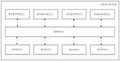
图1示出了根据本发明一个实施例的计算引擎的结构示意图,可应用于GPGPU处理器。该计算引擎100包括线程组构造单元110、指令缓存单元120、线程组管理单元130和计算核心单元140,其中计算核心单元140中包括寄存器文件单元。FIG. 1 shows a schematic structural diagram of a computing engine according to an embodiment of the present invention, which can be applied to a GPGPU processor. The computing engine 100 includes a thread group construction unit 110, an instruction cache unit 120, a thread group management unit 130 and a computing core unit 140, wherein the computing core unit 140 includes a register file unit.
线程组构造单元110用于将待处理的任务构造为多个线程组,其与线程组管理单元130和计算核心单元140具有通信连接,例如,可将该线程组内各个线程的初始位置信息写入计算核心单元140内的寄存器文件单元并将线程组的状态信息写入线程组管理单元130。The thread group construction unit 110 is used for constructing the tasks to be processed into a plurality of thread groups, which has a communication connection with the thread group management unit 130 and the computing core unit 140. For example, the initial position information of each thread in the thread group can be written. into the register file unit in the computing core unit 140 and write the thread group state information into the thread group management unit 130 .
线程组管理单元130用于对多个线程组进行调度,其与指令缓存单元120和计算核心单元140具有通信连接,例如,调度一个线程组去访问指令缓存单元120读取指令,以及将线程组对应的指令去计算核心单元140执行,每个线程组内的多个线程执行同一条程序指令。The thread group management unit 130 is used for scheduling multiple thread groups, and it has a communication connection with the instruction cache unit 120 and the computing core unit 140, for example, schedules a thread group to access the instruction cache unit 120 to read instructions, and assigns the thread group to the instruction cache unit 120. The corresponding instructions are executed by the computing core unit 140, and multiple threads in each thread group execute the same program instruction.
下文以大小为16线程的线程组为例,将单个线程组划分为4个大小为4线程的子线程组,每个子线程组对应计算核心单元140的一个寄存器文件单元,其他大小的线程组和子线程组也可以用类似的方式实现。Taking a thread group with a size of 16 threads as an example below, a single thread group is divided into 4 sub-thread groups with a size of 4 threads. Thread groups can also be implemented in a similar fashion.
图2示出计算核心单元的一个实施例,该计算核心单元140包括多个寄存器文件单元(示出为4个寄存器文件单元,分别标记为寄存器文件单元211-214)、交换网络220以及多个执行单元(示出了4个执行单元,分别标记为执行单元231-234),其中每个寄存器文件单元对应一个子线程组(即4个线程)。Figure 2 illustrates one embodiment of a computing core unit 140 comprising a plurality of register file units (shown as 4 register file units, labeled as register file units 211-214, respectively), a switching network 220, and a plurality of register file units Execution units (4 execution units are shown, labeled execution units 231-234, respectively), where each register file unit corresponds to a sub-thread group (ie, 4 threads).
每个寄存器文件单元用于接收线程组管理单元的程序指令(未示出),以及存放子线程组执行的程序指令相关的操作数和计算结果等。程序指令可包括最多三个操作数,操作数存储于寄存器文件单元的寄存器,以供执行程序时存取,例如,乘法指令包括两个操作数,乘累加指令包括三个操作数。Each register file unit is used for receiving program instructions (not shown) of the thread group management unit, and storing operands and calculation results related to the program instructions executed by the sub-thread group. A program instruction may include up to three operands, which are stored in registers in the register file unit for access during program execution, eg, a multiply instruction includes two operands, and a multiply-accumulate instruction includes three operands.
寄存器文件单元处理子线程组的读写请求,从寄存器中读取操作数以及向寄存器写入操作数,寄存器文件单元调度对各请求的处理,以免出现回写冲突。The register file unit processes read and write requests of the sub-thread group, reads operands from registers and writes operands to registers, and the register file unit schedules the processing of each request to avoid write-back conflicts.
执行单元用于执行程序指令,例如,执行乘累加指令,获得计算结果。The execution unit is used to execute program instructions, such as multiply-accumulate instructions, to obtain calculation results.
交换网络220用于寄存器文件单元和执行单元之间的数据交换,例如,将程序指令和相关操作数发送至执行单元以供处理。交换网络220可采用基于交叉开关的网络实现,设置为直连网络或树形网络等多种形式。Switch network 220 is used for data exchange between register file units and execution units, eg, sending program instructions and associated operands to the execution units for processing. The switching network 220 can be implemented by a network based on a crossbar switch, and can be set in various forms such as a direct-connected network or a tree-shaped network.
基于图2的实施例,数据处理过程是:线程组管理单元根据指令缓存单元获得的程序指令去相应寄存器文件单元读取源操作数;寄存器文件单元确定获得所有源操作数之后,将程序指令和相关的源操作数经由交换网络发送到执行单元,执行单元执行之后,将目的操作数经由交换网络写回到相应的寄存器文件单元。例如,对于乘累加程序指令,寄存器文件单元包括3个读取请求及一个写入请求。Based on the embodiment of FIG. 2, the data processing process is: the thread group management unit goes to the corresponding register file unit to read the source operand according to the program instruction obtained by the instruction cache unit; after the register file unit determines to obtain all the source operands, the program instruction and The relevant source operand is sent to the execution unit via the switching network, and after the execution unit executes, the destination operand is written back to the corresponding register file unit via the switching network. For example, for a multiply-accumulate program instruction, the register file unit includes three read requests and one write request.
在本发明中,对于一个寄存器文件单元,基于子线程组的线程数量组织寄存器文件单元中寄存器并且通过一定策略来调度操作数,使得寄存器文件单元能够使用单端口寄存器来模拟多端口寄存器。下文将根据本发明的一个实施例,介绍寄存器文件单元中寄存器的组织方式和数据调度方式。In the present invention, for a register file unit, the registers in the register file unit are organized based on the number of threads in the sub-thread group and operands are scheduled through a certain strategy, so that the register file unit can use single-port registers to simulate multi-port registers. Hereinafter, according to an embodiment of the present invention, the organization method and data scheduling method of the registers in the register file unit will be introduced.
图3示出了根据本发明一个实施例的寄存器文件单元的内部结构图,该寄存器文件单元300包括写操作调度单元310、读操作调度单元320和多个寄存器组,其中示出了4个寄存器组,分别标记为寄存器组0-3。FIG. 3 shows an internal structure diagram of a register file unit according to an embodiment of the present invention. The register file unit 300 includes a write operation scheduling unit 310, a read operation scheduling unit 320 and a plurality of register groups, among which 4 registers are shown Groups, labeled Register Groups 0-3, respectively.
写操作调度单元310用于处理写请求,将子线程组关联的写操作数按照一定的规则(下文将对其进行详细描述)进行调度,以使能够利用单端口寄存器实现写操作。The write operation scheduling unit 310 is used to process the write request, and schedule the write operation numbers associated with the sub-thread group according to certain rules (which will be described in detail below), so that the single-port register can be used to implement the write operation.
读操作调度单元320用于处理读请求,将子线程组关联的读操作数经调度组织为使得寄存器文件单元能够使用单端口寄存器实现读操作。The read operation scheduling unit 320 is used to process the read request, and organize the read operands associated with the sub-thread group through scheduling so that the register file unit can use the single-port register to implement the read operation.
寄存器组0-3用于存储与子线程组关联的操作数,包括读操作数和写操作数,每个寄存器组包含多个寄存器,对于包括4个线程的子线程组,通过适当调度读写操作数,能够使用单端口存储器模拟多端口存储器的功能。Register banks 0-3 are used to store operands associated with sub-thread groups, including read and write operands, each register bank contains multiple registers, and for sub-thread groups including 4 threads, read and write by appropriate scheduling Operands that can use a single-port memory to emulate the functionality of a multi-port memory.
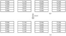
在一个实施例中,将寄存器文件单元300中的寄存器组织为图4的形式,划分为与子线程组的线程数量相等的多个寄存器组,例如,子线程组有4个线程时,划分出4个存储区,分别标记为寄存器组0-3,子线程组中的线程依次标记为T0、T1、T2、T3。该实施例的组织方式为:对于寄存器组0,四个线程T0、T1、T2、T3关联的操作数分别对应寄存器R4、R3、R2、R1,线程T0还对应寄存器R0;对于寄存器组1,四个线程T0、T1、T2、T3关联的操作数分别对应寄存器R1、R4、R3、R2,线程T1对应R0,对于其他寄存器组的组织方式类似,具体可参见图4所示。In one embodiment, the registers in the register file unit 300 are organized in the form of FIG. 4 and divided into multiple register groups equal to the number of threads in the sub-thread group. For example, when the sub-thread group has 4 threads, the The four storage areas are marked as register groups 0-3 respectively, and the threads in the sub-thread group are marked as T0, T1, T2, and T3 in turn. This embodiment is organized as follows: for
图4所示的组织方式具有以下特征:从寄存器的视角来看,4个线程的寄存器R0均放在四个寄存器组的同一位置0,寄存器R1均放在四个寄存器组的同一位置1,相应地,寄存器Rn均放在四个寄存器的同一位置n。从线程的视角来看,每个线程的寄存器均匀分布在4个寄存器组内。例如,线程T0的寄存器R0分布在寄存器组0,R1分布在寄存器组1,R2分布在寄存器组2,R3分布在寄存器组3;线程T1的寄存器R0分布在寄存器组1,R1分布在寄存器组2,R2分布在寄存器组3,R3分布在寄存器组0。简言之,线程Tn(n<4)的寄存器R0分布在寄存器组n,R1分布在寄存器组(n+1)%4,R2分布在寄存器组(n+2)%4,R3分布在寄存器组(n+3)%4。The organization shown in Figure 4 has the following characteristics: from the perspective of registers, the registers R0 of the four threads are placed in the
利用图4的寄存器组织方式,对于读写操作经过调度可采用单端口存储器实现多端口存储器的功能。Using the register organization method in FIG. 4 , single-port memory can be used to realize the function of multi-port memory after scheduling of read and write operations.
在一个实施例中,对于读寄存器操作,从寄存器组读出的源操作数为图5(a)所示,对于线程T0,其关联的寄存器R0位于从左向右数第一列,R1位于第二列,R2位于第三列,R3位于第四列,R4又回到第一列,类似地,对于线程T1,其关联的寄存器R0位于从左至右数第二列,R1位于第三列,R2位于第四列,R3位于第一列,R4又回到第二列。在读出源操作数之后,经由读操作调度单元的调度排序,组织为图5(b)所示的形式,即将线程T0关联的R0,R1,R2,R3,R4均调整到位于左至右数第一列,相应地,与T1关联的源操作数均位于第二列,与线程T2关联的源操作数均位于第三列,与线程T3关联的源操作数均位于第四列。In one embodiment, for a read register operation, the source operand read from the register set is as shown in Figure 5(a). For thread T0, its associated register R0 is located in the first column from left to right, and R1 is located in the first column from left to right. In the second column, R2 is in the third column, R3 is in the fourth column, and R4 is back in the first column. Similarly, for thread T1, its associated register R0 is in the second column from left to right, and R1 is in the third column. column, R2 is in the fourth column, R3 is in the first column, and R4 is back in the second column. After reading out the source operand, through the scheduling order of the read operation scheduling unit, the organization is in the form shown in Figure 5(b), that is, the R0, R1, R2, R3, and R4 associated with the thread T0 are adjusted to be located from left to right Counting the first column, correspondingly, the source operands associated with T1 are located in the second column, the source operands associated with thread T2 are located in the third column, and the source operands associated with thread T3 are located in the fourth column.
需要说明的是,图5(a)示出的R0,R1,R2,R3,R4等表示寄存器位置,而图5(b)示出的R0,R1,R2,R3,R4等表示的是从图5(a)中相应寄存器读出的数据。It should be noted that R0, R1, R2, R3, R4, etc. shown in Fig. 5(a) represent the register positions, while R0, R1, R2, R3, R4, etc. shown in Fig. 5(b) represent registers from The data read from the corresponding register in Figure 5(a).
经过读操作调度单元的调度排序之后,每个线程的操作数位于同一列,而线程与执行单元间存在一一对应的关系。例如,子线程组的T0对应于执行单元0,T1对应于执行单元1,T2对应于执行单元2,T3对应于执行单元3。通过调度单元的排序之后,每个线程的操作数均被调整至相应列中,从而可经由交换网络直接发送至相应的执行单元去执行。After the scheduling and sorting of the read operation scheduling unit, the operands of each thread are located in the same column, and there is a one-to-one correspondence between threads and execution units. For example, T0 of the child thread group corresponds to
在一个实施例中,对于写寄存器操作,采用与读寄存器相反的过程,即当写操作调度单元接收到写请求时,将各线程的写操作数组织为图5(a)所示的形式。In one embodiment, for the write register operation, a process opposite to the read register operation is adopted, that is, when the write operation scheduling unit receives a write request, the write operands of each thread are organized into the form shown in FIG. 5(a).
图6以存在四个子线程组为例,示意了寄存器的读写过程,其中,四个子线程组按照相位错开一个周期依次读取三个源操作数。具体而言,在第一个时钟周期0,第一个子线程组读取第一个源操作数SRC0;周期1,第一个子线程组读取第二个源操作数SRC1,第二个子线程组读取第一个源操作数SRC0;周期2,第一个子线程组读取第三个源操作数SRC2,第二个子线程组读取第二个源操作数SRC1,第三个子线程组读取第一个源操作数SRC0;周期3,第二个子线程组读取第三个源操作数SRC2,第三个子线程组读取第二个源操作数SRC1,第四个子线程组读取第一个源操作数SRC0。依此类推,直到所有源操作数读出后,四个子线程组以时分复用的方式共享同一组执行单元。通过这种调度方式,从子线程组的角度来看,第一个时钟周期读取第一个源操作数,第二个周期读取第二个源操作数,第三个周期读取第三个源操作数,由于通常最多只有三个源操作数,第四个周期可用于其他线程组相应子线程组操作数的写回。通过这种调度方式,每个寄存器文件单元的寄存器组每个周期最多只有一个读操作或者写操作,因而可以通过单端口存储器模拟多端口存储器来实现寄存器文件单元。FIG. 6 illustrates the process of reading and writing a register by taking the existence of four sub-thread groups as an example, wherein the four sub-thread groups sequentially read three source operands with a phase shift of one cycle. Specifically, in the
对于向量访存指令,每个线程一次可取回4个32位数据,每个线程的4个32位数据需同时写回到寄存器以提高性能。通过采用图4所示的寄存器组织方式,利用写操作调度单元的调度排序,任意四个连续目的地址的32位数据均可以同时写回到寄存器组内,即可同时写回R0R1R2R3、R1R2R3R4等,任意4个连续目的地址的寄存器均匀分布在四个寄存器组内。寄存器的这种组织方式避免了不必要的硬件限制,从而允许对寄存器的使用做更好的优化。For vector memory fetch instructions, each thread can retrieve 4 32-bit data at a time, and each thread's 4 32-bit data needs to be written back to the register at the same time to improve performance. By adopting the register organization method shown in Figure 4 and using the scheduling order of the write operation scheduling unit, the 32-bit data of any four consecutive destination addresses can be written back to the register group at the same time, that is, R0R1R2R3, R1R2R3R4, etc. can be written back at the same time. The registers of any 4 consecutive destination addresses are evenly distributed in the four register groups. This organization of registers avoids unnecessary hardware constraints, allowing better optimization of register usage.
应理解的是,上述实施例仅用于示意性的描述,本发明的思想适用于任何数量的子线程组,子线程组包含的线程数可以是任意个,并且本发明适用于任何位数的标量数据和向量数据的访存。此外,读操作调度单元和写操作调度单元可集成为一个调度单元。It should be understood that the above embodiments are only for illustrative description, the idea of the present invention is applicable to any number of sub-thread groups, the number of threads contained in the sub-thread group may be any number, and the present invention is applicable to any number of threads. Access to scalar data and vector data. In addition, the read operation scheduling unit and the write operation scheduling unit may be integrated into one scheduling unit.
本发明提供的管理寄存器文件单元的方法或者说使用单端口存储器模拟多端口存储器的方法,可应用于任何包含寄存器文件单元的电子设备,例如、台式计算机、便携式计算机、平板电脑、智能手机或任何其他类型的计算设备(例如,基于GPGPU的设备)。本发明的电子设备可应用于文字处理、语音识别与处理、多国语言翻译、图像识别、生物特征识到、智能控制等领域,可用作智能计算处理设备、机器人、移动设备等。The method for managing register file units provided by the present invention, or the method for simulating multi-port memory using single-port memory, can be applied to any electronic device containing register file units, such as desktop computers, portable computers, tablet computers, smart phones or any Other types of computing devices (eg, GPGPU-based devices). The electronic device of the present invention can be applied to the fields of word processing, speech recognition and processing, multi-language translation, image recognition, biometric recognition, intelligent control, etc., and can be used as intelligent computing processing equipment, robots, mobile equipment, and the like.
需要说明的是,虽然上文按照特定顺序描述了各个步骤,但是并不意味着必须按照上述特定顺序来执行各个步骤,实际上,这些步骤中的一些可以并发执行,甚至改变顺序,只要能够实现所需要的功能即可。It should be noted that although the steps are described above in a specific order, it does not mean that the steps must be executed in the above-mentioned specific order. In fact, some of these steps can be executed concurrently, or even change the order, as long as it can be achieved The required function can be.
本发明可以是系统、方法和/或计算机程序产品。计算机程序产品可以包括计算机可读存储介质,其上载有用于使处理器实现本发明的各个方面的计算机可读程序指令。The present invention may be a system, method and/or computer program product. The computer program product may include a computer-readable storage medium having computer-readable program instructions loaded thereon for causing a processor to implement various aspects of the present invention.
计算机可读存储介质可以是保持和存储由指令执行设备使用的指令的有形设备。计算机可读存储介质例如可以包括但不限于电存储设备、磁存储设备、光存储设备、电磁存储设备、半导体存储设备或者上述的任意合适的组合。计算机可读存储介质的更具体的例子(非穷举的列表)包括:便携式计算机盘、硬盘、随机存取存储器(RAM)、只读存储器(ROM)、可擦式可编程只读存储器(EPROM或闪存)、静态随机存取存储器(SRAM)、便携式压缩盘只读存储器(CD-ROM)、数字多功能盘(DVD)、记忆棒、软盘、机械编码设备、例如其上存储有指令的打孔卡或凹槽内凸起结构、以及上述的任意合适的组合。A computer-readable storage medium may be a tangible device that retains and stores instructions for use by the instruction execution device. Computer-readable storage media may include, but are not limited to, electrical storage devices, magnetic storage devices, optical storage devices, electromagnetic storage devices, semiconductor storage devices, or any suitable combination of the foregoing, for example. More specific examples (non-exhaustive list) of computer readable storage media include: portable computer disks, hard disks, random access memory (RAM), read only memory (ROM), erasable programmable read only memory (EPROM) or flash memory), static random access memory (SRAM), portable compact disk read only memory (CD-ROM), digital versatile disk (DVD), memory sticks, floppy disks, mechanically coded devices, such as printers with instructions stored thereon Hole cards or raised structures in grooves, and any suitable combination of the above.
附图中的流程图和框图显示了根据本发明的多个实施例的系统、方法和计算机程序产品的可能实现的体系架构、功能和操作。在这点上,流程图或框图中的每个方框可以代表一个模块、程序段或指令的一部分,所述模块、程序段或指令的一部分包含一个或多个用于实现规定的逻辑功能的可执行指令。在有些作为替换的实现中,方框中所标注的功能也可以以不同于附图中所标注的顺序发生。例如,两个连续的方框实际上可以基本并行地执行,它们有时也可以按相反的顺序执行,这依所涉及的功能而定。也要注意的是,框图和/或流程图中的每个方框、以及框图和/或流程图中的方框的组合,可以利用执行规定的功能或动作的专用的基于硬件的系统来实现,或者可以用专用硬件与计算机指令的组合来实现。对于本领域技术人员来说公知的是,通过硬件方式实现、通过软件方式实现以及通过软件和硬件结合的方式实现都是等价的。The flowchart and block diagrams in the Figures illustrate the architecture, functionality, and operation of possible implementations of systems, methods and computer program products according to various embodiments of the present invention. In this regard, each block in the flowchart or block diagrams may represent a module, segment, or portion of instructions, which comprises one or more functions for implementing the specified logical function(s) executable instructions. In some alternative implementations, the functions noted in the blocks may occur out of the order noted in the figures. For example, two blocks in succession may, in fact, be executed substantially concurrently, or the blocks may sometimes be executed in the reverse order, depending upon the functionality involved. It is also noted that each block of the block diagrams and/or flowchart illustrations, and combinations of blocks in the block diagrams and/or flowchart illustrations, can be implemented using dedicated hardware-based systems that perform the specified functions or actions , or can be implemented in a combination of dedicated hardware and computer instructions. It is well known to those skilled in the art that implementation in hardware, implementation in software, and implementation in a combination of software and hardware are all equivalent.
以上已经描述了本发明的各实施例,上述说明是示例性的,并非穷尽性的,并且也不限于所披露的各实施例。在不偏离所说明的各实施例的范围和精神的情况下,对于本技术领域的普通技术人员来说许多修改和变更都是显而易见的。本文中所用术语的选择,旨在最好地解释各实施例的原理、实际应用或对市场中的技术改进,或者使本技术领域的其它普通技术人员能理解本文披露的各实施例。Various embodiments of the present invention have been described above, and the foregoing descriptions are exemplary, not exhaustive, and not limiting of the disclosed embodiments. Numerous modifications and variations will be apparent to those of ordinary skill in the art without departing from the scope and spirit of the described embodiments. The terminology used herein was chosen to best explain the principles of the embodiments, the practical application or technical improvement in the marketplace, or to enable others of ordinary skill in the art to understand the embodiments disclosed herein.
Claims (12)
Translated fromChinesePriority Applications (1)
| Application Number | Priority Date | Filing Date | Title |
|---|---|---|---|
| CN201910052633.XACN111459543B (en) | 2019-01-21 | 2019-01-21 | Method for managing register file unit |
Applications Claiming Priority (1)
| Application Number | Priority Date | Filing Date | Title |
|---|---|---|---|
| CN201910052633.XACN111459543B (en) | 2019-01-21 | 2019-01-21 | Method for managing register file unit |
Publications (2)
| Publication Number | Publication Date |
|---|---|
| CN111459543A CN111459543A (en) | 2020-07-28 |
| CN111459543Btrue CN111459543B (en) | 2022-09-13 |
Family
ID=71679088
Family Applications (1)
| Application Number | Title | Priority Date | Filing Date |
|---|---|---|---|
| CN201910052633.XAActiveCN111459543B (en) | 2019-01-21 | 2019-01-21 | Method for managing register file unit |
Country Status (1)
| Country | Link |
|---|---|
| CN (1) | CN111459543B (en) |
Families Citing this family (5)
| Publication number | Priority date | Publication date | Assignee | Title |
|---|---|---|---|---|
| CN115129369B (en)* | 2021-03-26 | 2025-03-28 | 上海阵量智能科技有限公司 | Command distribution method, command distributor, chip and electronic device |
| CN114546329B (en)* | 2022-03-01 | 2023-07-18 | 上海壁仞智能科技有限公司 | Method, apparatus and medium for implementing data parity rearrangement |
| CN114546328B (en)* | 2022-03-01 | 2025-02-11 | 上海壁仞科技股份有限公司 | Method, device and medium for implementing data arrangement |
| CN115129480B (en)* | 2022-08-26 | 2022-11-08 | 上海登临科技有限公司 | Access control method for scalar processing unit and scalar processing unit |
| CN118626146B (en)* | 2024-08-08 | 2024-10-29 | 北京壁仞科技开发有限公司 | Artificial intelligence chip, register space dynamic management method, medium and program |
Citations (2)
| Publication number | Priority date | Publication date | Assignee | Title |
|---|---|---|---|---|
| CN103218208A (en)* | 2011-12-06 | 2013-07-24 | 辉达公司 | System and method for performing shaped memory access operations |
| CN103257931A (en)* | 2011-12-22 | 2013-08-21 | 辉达公司 | Shaped register file reads |
Family Cites Families (6)
| Publication number | Priority date | Publication date | Assignee | Title |
|---|---|---|---|---|
| US6546461B1 (en)* | 2000-11-22 | 2003-04-08 | Integrated Device Technology, Inc. | Multi-port cache memory devices and FIFO memory devices having multi-port cache memory devices therein |
| AU2003300303A1 (en)* | 2002-12-31 | 2004-07-29 | Globespanvirata Incorporated | System and method for providing quality of service in asynchronous transfer mode cell transmission |
| US7339592B2 (en)* | 2004-07-13 | 2008-03-04 | Nvidia Corporation | Simulating multiported memories using lower port count memories |
| US8533435B2 (en)* | 2009-09-24 | 2013-09-10 | Nvidia Corporation | Reordering operands assigned to each one of read request ports concurrently accessing multibank register file to avoid bank conflict |
| US8458446B2 (en)* | 2009-09-30 | 2013-06-04 | Oracle America, Inc. | Accessing a multibank register file using a thread identifier |
| US10303472B2 (en)* | 2016-11-22 | 2019-05-28 | Advanced Micro Devices, Inc. | Bufferless communication for redundant multithreading using register permutation |
- 2019
- 2019-01-21CNCN201910052633.XApatent/CN111459543B/enactiveActive
Patent Citations (2)
| Publication number | Priority date | Publication date | Assignee | Title |
|---|---|---|---|---|
| CN103218208A (en)* | 2011-12-06 | 2013-07-24 | 辉达公司 | System and method for performing shaped memory access operations |
| CN103257931A (en)* | 2011-12-22 | 2013-08-21 | 辉达公司 | Shaped register file reads |
Non-Patent Citations (1)
| Title |
|---|
| 一种基于活跃周期的低端口数低能耗寄存器堆设计;赵雨来等;《计算机学报》;20080215(第02期);117-126* |
Also Published As
| Publication number | Publication date |
|---|---|
| CN111459543A (en) | 2020-07-28 |
Similar Documents
| Publication | Publication Date | Title |
|---|---|---|
| CN111459543B (en) | Method for managing register file unit | |
| KR102780371B1 (en) | Method for performing PIM (PROCESSING-IN-MEMORY) operations on serially allocated data, and related memory devices and systems | |
| CN109997115B (en) | Low power and low latency GPU co-processor for persistent computation | |
| US5832290A (en) | Apparatus, systems and method for improving memory bandwidth utilization in vector processing systems | |
| US11500802B1 (en) | Data replication for accelerator | |
| US7634621B1 (en) | Register file allocation | |
| US20180121386A1 (en) | Super single instruction multiple data (super-simd) for graphics processing unit (gpu) computing | |
| US20100023728A1 (en) | Method and system for in-place multi-dimensional transpose for multi-core processors with software-managed memory hierarchy | |
| WO2017185393A1 (en) | Apparatus and method for executing inner product operation of vectors | |
| US9626191B2 (en) | Shaped register file reads | |
| JP7264897B2 (en) | Memory device and method for controlling same | |
| US10223269B2 (en) | Method and apparatus for preventing bank conflict in memory | |
| JP6551751B2 (en) | Multiprocessor device | |
| US20150082007A1 (en) | Register mapping with multiple instruction sets | |
| US8539207B1 (en) | Lattice-based computations on a parallel processor | |
| CN112486904A (en) | Register file design method and device for reconfigurable processing unit array | |
| CN115248701B (en) | Zero-copy data transmission device and method between processor register files | |
| CN108717402B (en) | Memory and Reconfigurable Processing System for Reconfigurable Processing System | |
| KR102644951B1 (en) | Arithmetic Logic Unit Register Sequencing | |
| US12099842B2 (en) | Arithmetic processing device and arithmetic processing method | |
| Motokubota et al. | Accelerating parameter sweep applications using CUDA | |
| KR20250058533A (en) | Memory device and method with processing-in-memory | |
| JP2015191463A (en) | Arithmetic processing device and control method of arithmetic processing device | |
| JPH05265749A (en) | Register file circuit |
Legal Events
| Date | Code | Title | Description |
|---|---|---|---|
| PB01 | Publication | ||
| PB01 | Publication | ||
| SE01 | Entry into force of request for substantive examination | ||
| SE01 | Entry into force of request for substantive examination | ||
| GR01 | Patent grant | ||
| GR01 | Patent grant | ||
| EE01 | Entry into force of recordation of patent licensing contract | ||
| EE01 | Entry into force of recordation of patent licensing contract | Application publication date:20200728 Assignee:Suzhou Heyu Finance Leasing Co.,Ltd. Assignor:Shanghai Denglin Technology Co.,Ltd. Contract record no.:X2024980007796 Denomination of invention:A method for managing register file units Granted publication date:20220913 License type:Exclusive License Record date:20240625 | |
| PE01 | Entry into force of the registration of the contract for pledge of patent right | ||
| PE01 | Entry into force of the registration of the contract for pledge of patent right | Denomination of invention:A method for managing register file units Granted publication date:20220913 Pledgee:Suzhou Heyu Finance Leasing Co.,Ltd. Pledgor:Shanghai Denglin Technology Co.,Ltd. Registration number:Y2024980025096 | |
| CP03 | Change of name, title or address | ||
| CP03 | Change of name, title or address | Address after:Room 1101, Building 5, South Bank New Land Phase I, No. 11 Yangfu Road, Suzhou Industrial Park, Suzhou Area, China (Jiangsu) Pilot Free Trade Zone, Suzhou City, Jiangsu Province 215101 Patentee after:Suzhou Denglin Technology Co.,Ltd. Country or region after:China Address before:Room 901, 570 shengxia Road, Pudong New Area, Shanghai 201203 Patentee before:Shanghai Denglin Technology Co.,Ltd. Country or region before:China |