CN111450907B - Microfluidic device, sample mixing method, and microfluidic system - Google Patents
Microfluidic device, sample mixing method, and microfluidic systemDownload PDFInfo
- Publication number
- CN111450907B CN111450907BCN202010337805.0ACN202010337805ACN111450907BCN 111450907 BCN111450907 BCN 111450907BCN 202010337805 ACN202010337805 ACN 202010337805ACN 111450907 BCN111450907 BCN 111450907B
- Authority
- CN
- China
- Prior art keywords
- electrode
- microfluidic device
- channel
- substrate
- sub
- Prior art date
- Legal status (The legal status is an assumption and is not a legal conclusion. Google has not performed a legal analysis and makes no representation as to the accuracy of the status listed.)
- Expired - Fee Related
Links
Images


Classifications
- B—PERFORMING OPERATIONS; TRANSPORTING
- B01—PHYSICAL OR CHEMICAL PROCESSES OR APPARATUS IN GENERAL
- B01L—CHEMICAL OR PHYSICAL LABORATORY APPARATUS FOR GENERAL USE
- B01L3/00—Containers or dishes for laboratory use, e.g. laboratory glassware; Droppers
- B01L3/50—Containers for the purpose of retaining a material to be analysed, e.g. test tubes
- B01L3/502—Containers for the purpose of retaining a material to be analysed, e.g. test tubes with fluid transport, e.g. in multi-compartment structures
- B01L3/5027—Containers for the purpose of retaining a material to be analysed, e.g. test tubes with fluid transport, e.g. in multi-compartment structures by integrated microfluidic structures, i.e. dimensions of channels and chambers are such that surface tension forces are important, e.g. lab-on-a-chip
- B—PERFORMING OPERATIONS; TRANSPORTING
- B01—PHYSICAL OR CHEMICAL PROCESSES OR APPARATUS IN GENERAL
- B01F—MIXING, e.g. DISSOLVING, EMULSIFYING OR DISPERSING
- B01F33/00—Other mixers; Mixing plants; Combinations of mixers
- B01F33/05—Mixers using radiation, e.g. magnetic fields or microwaves to mix the material
- B—PERFORMING OPERATIONS; TRANSPORTING
- B01—PHYSICAL OR CHEMICAL PROCESSES OR APPARATUS IN GENERAL
- B01F—MIXING, e.g. DISSOLVING, EMULSIFYING OR DISPERSING
- B01F33/00—Other mixers; Mixing plants; Combinations of mixers
- B01F33/30—Micromixers
- B01F33/305—Micromixers using mixing means not otherwise provided for
- B—PERFORMING OPERATIONS; TRANSPORTING
- B01—PHYSICAL OR CHEMICAL PROCESSES OR APPARATUS IN GENERAL
- B01F—MIXING, e.g. DISSOLVING, EMULSIFYING OR DISPERSING
- B01F33/00—Other mixers; Mixing plants; Combinations of mixers
- B01F33/40—Mixers using gas or liquid agitation, e.g. with air supply tubes
- B01F33/403—Mixers using gas or liquid agitation, e.g. with air supply tubes for mixing liquids
- B—PERFORMING OPERATIONS; TRANSPORTING
- B01—PHYSICAL OR CHEMICAL PROCESSES OR APPARATUS IN GENERAL
- B01F—MIXING, e.g. DISSOLVING, EMULSIFYING OR DISPERSING
- B01F33/00—Other mixers; Mixing plants; Combinations of mixers
- B01F33/40—Mixers using gas or liquid agitation, e.g. with air supply tubes
- B01F33/409—Parts, e.g. diffusion elements; Accessories
- B—PERFORMING OPERATIONS; TRANSPORTING
- B01—PHYSICAL OR CHEMICAL PROCESSES OR APPARATUS IN GENERAL
- B01L—CHEMICAL OR PHYSICAL LABORATORY APPARATUS FOR GENERAL USE
- B01L3/00—Containers or dishes for laboratory use, e.g. laboratory glassware; Droppers
- B01L3/50—Containers for the purpose of retaining a material to be analysed, e.g. test tubes
- B01L3/502—Containers for the purpose of retaining a material to be analysed, e.g. test tubes with fluid transport, e.g. in multi-compartment structures
- B01L3/5027—Containers for the purpose of retaining a material to be analysed, e.g. test tubes with fluid transport, e.g. in multi-compartment structures by integrated microfluidic structures, i.e. dimensions of channels and chambers are such that surface tension forces are important, e.g. lab-on-a-chip
- B01L3/50273—Containers for the purpose of retaining a material to be analysed, e.g. test tubes with fluid transport, e.g. in multi-compartment structures by integrated microfluidic structures, i.e. dimensions of channels and chambers are such that surface tension forces are important, e.g. lab-on-a-chip characterised by the means or forces applied to move the fluids
- B—PERFORMING OPERATIONS; TRANSPORTING
- B01—PHYSICAL OR CHEMICAL PROCESSES OR APPARATUS IN GENERAL
- B01L—CHEMICAL OR PHYSICAL LABORATORY APPARATUS FOR GENERAL USE
- B01L3/00—Containers or dishes for laboratory use, e.g. laboratory glassware; Droppers
- B01L3/50—Containers for the purpose of retaining a material to be analysed, e.g. test tubes
- B01L3/502—Containers for the purpose of retaining a material to be analysed, e.g. test tubes with fluid transport, e.g. in multi-compartment structures
- B01L3/5027—Containers for the purpose of retaining a material to be analysed, e.g. test tubes with fluid transport, e.g. in multi-compartment structures by integrated microfluidic structures, i.e. dimensions of channels and chambers are such that surface tension forces are important, e.g. lab-on-a-chip
- B01L3/502769—Containers for the purpose of retaining a material to be analysed, e.g. test tubes with fluid transport, e.g. in multi-compartment structures by integrated microfluidic structures, i.e. dimensions of channels and chambers are such that surface tension forces are important, e.g. lab-on-a-chip characterised by multiphase flow arrangements
- B01L3/502784—Containers for the purpose of retaining a material to be analysed, e.g. test tubes with fluid transport, e.g. in multi-compartment structures by integrated microfluidic structures, i.e. dimensions of channels and chambers are such that surface tension forces are important, e.g. lab-on-a-chip characterised by multiphase flow arrangements specially adapted for droplet or plug flow, e.g. digital microfluidics
- G—PHYSICS
- G01—MEASURING; TESTING
- G01N—INVESTIGATING OR ANALYSING MATERIALS BY DETERMINING THEIR CHEMICAL OR PHYSICAL PROPERTIES
- G01N1/00—Sampling; Preparing specimens for investigation
- G01N1/28—Preparing specimens for investigation including physical details of (bio-)chemical methods covered elsewhere, e.g. G01N33/50, C12Q
- G01N1/38—Diluting, dispersing or mixing samples
- B—PERFORMING OPERATIONS; TRANSPORTING
- B01—PHYSICAL OR CHEMICAL PROCESSES OR APPARATUS IN GENERAL
- B01L—CHEMICAL OR PHYSICAL LABORATORY APPARATUS FOR GENERAL USE
- B01L2400/00—Moving or stopping fluids
- B01L2400/04—Moving fluids with specific forces or mechanical means
- B01L2400/0403—Moving fluids with specific forces or mechanical means specific forces
- B01L2400/0415—Moving fluids with specific forces or mechanical means specific forces electrical forces, e.g. electrokinetic
Landscapes
- Chemical & Material Sciences (AREA)
- Health & Medical Sciences (AREA)
- Chemical Kinetics & Catalysis (AREA)
- General Health & Medical Sciences (AREA)
- Dispersion Chemistry (AREA)
- Analytical Chemistry (AREA)
- Hematology (AREA)
- Clinical Laboratory Science (AREA)
- General Physics & Mathematics (AREA)
- Immunology (AREA)
- Pathology (AREA)
- Biochemistry (AREA)
- Life Sciences & Earth Sciences (AREA)
- Physics & Mathematics (AREA)
- Physical Or Chemical Processes And Apparatus (AREA)
- Automatic Analysis And Handling Materials Therefor (AREA)
Abstract
Description
Translated fromChinese技术领域technical field
本申请涉及微流控技术领域,尤其涉及一种微流控器件、样品混匀方法、微流控系统。The present application relates to the technical field of microfluidics, and in particular, to a microfluidic device, a sample mixing method, and a microfluidic system.
背景技术Background technique
微流控技术(Microfluidics)是一种精确控制和操控微尺度流体的技术,通过此技术,研究人员可以把样品制备、反应、分离、检测等基本操作单元集成到一块厘米级芯片上。微流控技术一般应用于生物、化学、制药等领域的微量药品的分析过程,它主要涉及微量试剂的混匀、输运等。其中样品的混匀是生化检测的重要步骤之一,对于生物医疗、药物诊断、食品卫生、环境监测及分子生物学等领域的发展具有重要的意义。Microfluidics is a technology for precise control and manipulation of micro-scale fluids. Through this technology, researchers can integrate basic operating units such as sample preparation, reaction, separation, and detection into a centimeter-scale chip. Microfluidic technology is generally used in the analysis process of trace drugs in the fields of biology, chemistry, pharmacy, etc. It mainly involves the mixing and transportation of trace reagents. Among them, sample mixing is one of the important steps in biochemical detection, which is of great significance to the development of biomedicine, drug diagnosis, food hygiene, environmental monitoring and molecular biology.
在现有的微流控技术中,样本混匀普遍在外部设备如摇床、离心机等设备中完成,这对于微流控芯片的集成化发展是十分不利的。如果于微流控芯片上完成样品的混匀孵育等过程,在不使用复杂的外部驱动设备的前提下,普遍利用样品的浓度梯度或温度梯度通过扩散效应完成样品的混匀,此方法相对于主动混匀方法其混匀时间较长,不利于微流控芯片的检测效率提升。In the existing microfluidic technology, sample mixing is generally done in external equipment such as shakers, centrifuges, etc., which is very unfavorable for the integrated development of microfluidic chips. If the process of mixing and incubating the sample is completed on the microfluidic chip, the concentration gradient or temperature gradient of the sample is generally used to complete the mixing of the sample through the diffusion effect without the use of complex external driving equipment. The active mixing method has a long mixing time, which is not conducive to the improvement of the detection efficiency of the microfluidic chip.
综上,现有技术无法在微流控芯片上进行样品快速混匀,影响微流控芯片的检测效率。To sum up, the prior art cannot quickly mix samples on the microfluidic chip, which affects the detection efficiency of the microfluidic chip.
发明内容SUMMARY OF THE INVENTION
本申请实施例提供了一种微流控器件、样品混匀方法、微流控系统,用以在微流控器件上进行样品快速混匀,提高微流控器件的检测效率。The embodiments of the present application provide a microfluidic device, a sample mixing method, and a microfluidic system, which are used to rapidly mix samples on the microfluidic device and improve the detection efficiency of the microfluidic device.
本申请实施例提供的一种微流控器件,所述微流控芯片包括:对盒设置的下基板和上基板;In a microfluidic device provided by an embodiment of the present application, the microfluidic chip includes: a lower substrate and an upper substrate arranged in a box;
所述下基板包括:下衬底基板,位于所述下衬底基板面向所述上基板一侧的容纳液滴的微流道;The lower substrate includes: a lower substrate substrate, a micro-flow channel for accommodating droplets on the side of the lower substrate substrate facing the upper substrate;
所述上基板包括:上衬底基板,位于所述上衬底基板面向所述下基板一侧的多个电极组,位于所述电极组面向所述下基板一侧的介质层;The upper substrate includes: an upper substrate substrate, a plurality of electrode groups located on the side of the upper substrate substrate facing the lower substrate, and a dielectric layer located on the side of the electrode group facing the lower substrate;
所述电极组的正投影落入所述微流道的正投影内;The orthographic projection of the electrode group falls within the orthographic projection of the microfluidic channel;
所述电极组被配置为:对所述电极组施加电压,以使所述介质层发生可逆介电击穿。The electrode group is configured to apply a voltage to the electrode group to cause reversible dielectric breakdown of the dielectric layer.
本申请实施例提供的微流控器件,由于在上基板设置有介质层以及电极组,对电极组施加电压可以使得介质层发生可逆介电击穿,从而可以使得在微流道内待混匀样品的液滴电解产生气泡,利用气泡的搅拌效应实现了样品的快速混匀,提高在微流控器件内进行样品混匀的效率,从而提高微流控器件检测效率。In the microfluidic device provided by the embodiments of the present application, since the upper substrate is provided with a dielectric layer and an electrode group, applying a voltage to the electrode group can cause reversible dielectric breakdown of the dielectric layer, so that the sample to be mixed in the microfluidic channel can be homogeneously The droplet electrolysis generates bubbles, and the stirring effect of the bubbles is used to realize the rapid mixing of the sample, which improves the efficiency of sample mixing in the microfluidic device, thereby improving the detection efficiency of the microfluidic device.
可选地,所述微流道包括:沿第一方向延伸的主流道,以及与所述主流道交汇的多对支流道;Optionally, the micro flow channel includes: a main flow channel extending along the first direction, and a plurality of pairs of branch flow channels intersecting with the main flow channel;
每一对所述支流道包括:分别位于所述主流道两侧的第一支流道和第二支流道;Each pair of the branch channels includes: a first branch channel and a second branch channel respectively located on both sides of the main channel;
所述电极组的正投影落入所述主流道的正投影内。The orthographic projection of the electrode group falls within the orthographic projection of the main channel.
可选地,每一所述电极组包括沿第一方向排列的两个所述第一子电极,以及位于两个所述第一子电极之间的一个第二子电极;所述第一方向为所述主流道延伸的方向。Optionally, each of the electrode groups includes two first sub-electrodes arranged along a first direction, and one second sub-electrode located between the two first sub-electrodes; the first direction is the direction in which the main flow channel extends.
可选地,在第一方向上,所述第二子电极的宽度大于所述第一子电极的宽度。Optionally, in the first direction, the width of the second sub-electrode is greater than the width of the first sub-electrode.
可选地,在第一方向上,所述第一子电极的宽度和所述第二子电极的宽度均小于所述液滴的直径;且在第一方向上,当所述液滴中心的正投影与所述第二子电极的中心的正投影重合时,所述液滴的正投影与两个所述第一子电极的正投影均有交叠。Optionally, in the first direction, the width of the first sub-electrode and the width of the second sub-electrode are both smaller than the diameter of the drop; and in the first direction, when the center of the drop is When the orthographic projection coincides with the orthographic projection of the center of the second sub-electrode, the orthographic projection of the droplet overlaps with the orthographic projection of the two first sub-electrodes.
本申请实施例提供的微流控器件,电极组中各电极的尺寸设计考虑了液滴的直径,使需要混匀的样品的液滴的中心正投影与第二子电极中心正投影重合时,液滴还覆盖第一子电极的区域,从而可以确保液滴覆盖区域的介质层发生点击穿,使液滴电解产生气泡以实现样品混匀。In the microfluidic device provided by the embodiment of the present application, the size of each electrode in the electrode group is designed considering the diameter of the droplet, so that when the center orthographic projection of the droplet of the sample to be mixed is coincident with the center orthographic projection of the second sub-electrode, The droplet also covers the area of the first sub-electrode, so that the dielectric layer in the area covered by the droplet can be ensured to tap through, so that the droplet is electrolyzed to generate air bubbles to achieve sample mixing.
可选地,所述上基板还包括:贯穿所述上衬底基板的第一入液孔、多个第二入液孔、多个第三入液孔、以及出液孔;Optionally, the upper substrate further comprises: a first liquid inlet hole, a plurality of second liquid inlet holes, a plurality of third liquid inlet holes, and a liquid outlet hole penetrating the upper substrate substrate;
在所述下衬底基板上,所述第一入液孔的正投影在所述主流道的起点区域与所述主流道的正投影有交叠,所述出液孔在所述主流道的终点区域与所述主流道的正投影有交叠,所述第二入液孔的正投影在所述第一支流道的起点区域与所述第一支流道的正投影有交叠;所述第三入液孔的正投影在所述第二支流道的起点区域与所述第二支流道的正投影有交叠。On the lower substrate substrate, the orthographic projection of the first liquid inlet hole overlaps with the orthographic projection of the main flow channel at the starting point region of the main flow channel, and the liquid outlet hole is located at the edge of the main flow channel. The end area overlaps with the orthographic projection of the main channel, and the orthographic projection of the second liquid inlet hole overlaps with the orthographic projection of the first branch channel at the starting point area of the first branch channel; the The orthographic projection of the third liquid inlet hole overlaps with the orthographic projection of the second branch flow channel at the starting point region of the second branch flow channel.
可选地,所述电极组的数量等于所述支流道的对数,且每一所述电极组位于一对所述支流道远离所述第一入液孔的一侧。Optionally, the number of the electrode groups is equal to the number of pairs of the branch channels, and each of the electrode groups is located on a side of a pair of the branch channels away from the first liquid inlet hole.
可选地,所述下基板还包括:位于所述下衬底基板面向所述上基板一侧且位于所述微流道内的第一电极层;所述第一电极层至少位于所述主流道内。Optionally, the lower substrate further includes: a first electrode layer located on the side of the lower substrate facing the upper substrate and located in the micro channel; the first electrode layer is located at least in the main channel .
申请实施例提供的微流控器件,由于下基板还设置有第一电极层,第一电极层和电极组分别位于介质层两侧,从而可以通过第一电极层和电极组在介质层两侧形成容易使得介质层发生可逆介电击穿的电场。更容易实现对介质层可逆介电击穿范围的调控。In the microfluidic device provided by the application example, since the lower substrate is further provided with a first electrode layer, the first electrode layer and the electrode group are respectively located on both sides of the dielectric layer, so that the first electrode layer and the electrode group can be located on both sides of the dielectric layer through the first electrode layer and the electrode group. An electric field that can easily cause reversible dielectric breakdown of the dielectric layer is formed. It is easier to control the reversible dielectric breakdown range of the dielectric layer.
可选地,所述微流控器件还包括与所述第一电极层电连接的地电极;所述微流控器件还包括:与所述电极组电连接的驱动芯片。Optionally, the microfluidic device further includes a ground electrode electrically connected to the first electrode layer; the microfluidic device further includes: a driving chip electrically connected to the electrode group.
可选地,所述微流控器件还包括:在垂直于所述微流控器件所在平面方向上,分别位于所述微流道两侧的第一光学组件和第二光学组件;Optionally, the microfluidic device further comprises: a first optical component and a second optical component respectively located on both sides of the microfluidic channel in a direction perpendicular to the plane of the microfluidic device;
所述第一光学组件包括:第一滤光片;The first optical assembly includes: a first filter;
所述第二光学组件包括:第二滤光片,位于所述第二滤光片任一侧的微透镜阵列,位于所述微透镜阵列入光侧的准直平坦化层;The second optical component comprises: a second filter, a microlens array on either side of the second filter, and a collimation and flattening layer on the light incident side of the microlens array;
所述第一光学组件的正投影和所述第二光学组件的正投影至少覆盖所述微流道。The orthographic projection of the first optical component and the orthographic projection of the second optical component cover at least the microfluidic channel.
本申请实施例提供的微流控器件,将对样品进行光学检测的除光源以及光电探测器以外的光学组件设置在微流控器件内,即光学组件与微流控器件集成,进一步提升了微流控器件的集成度,并且无需进行复杂的光学对位,可以有效缩短光程,还可以减小光学检测系统的体积。并且由于第一滤光层和第二滤光层位于微流控器件内部,第一滤光层和第二滤光层距离待测样品的距离较近,通过第二滤光片的激发光经过较短的光程照射与样品,提高照射到样品的激发光光强,激发光通带较窄。而第一滤光层设置在微流控器件内,从而可以大大减小光电探测器与微流控器件的距离,光电探测器接收较强的荧光信号,可以提高检测信号的强度,从而提高检测准确率。In the microfluidic device provided by the embodiments of the present application, the optical components other than the light source and the photodetector for optical detection of the sample are arranged in the microfluidic device, that is, the optical components are integrated with the microfluidic device, which further improves the microfluidic device. The integration of the fluidic device and the need for complex optical alignment can effectively shorten the optical path and reduce the volume of the optical detection system. And because the first filter layer and the second filter layer are located inside the microfluidic device, the distance between the first filter layer and the second filter layer is relatively close to the sample to be tested, and the excitation light passing through the second filter passes through the microfluidic device. The shorter optical path irradiates the sample, increases the intensity of the excitation light irradiated to the sample, and the excitation light passband is narrower. The first filter layer is arranged in the microfluidic device, so that the distance between the photodetector and the microfluidic device can be greatly reduced. The photodetector receives a strong fluorescent signal, which can improve the intensity of the detection signal, thereby improving detection. Accuracy.
可选地,所述第二光学组件还包括:位于所述微透镜阵列和所述准直平坦化层之间的抗反射层。Optionally, the second optical assembly further includes: an anti-reflection layer located between the microlens array and the collimation and planarization layer.
本申请实施例提供的微流控器件,在准直平坦化层和微透镜阵列之间还设置有抗反射层,从而可以减少光到达不同截面产生的反射,减少光损失,提高照射到样品的光信号的强度,进而提高样品发车的荧光信号的强度,提高检测准确率。In the microfluidic device provided by the embodiment of the present application, an anti-reflection layer is further arranged between the collimation and flattening layer and the microlens array, so that the reflection caused by the light reaching different sections can be reduced, the light loss can be reduced, and the irradiated sample to the sample can be improved. The intensity of the light signal, thereby improving the intensity of the fluorescent signal emitted by the sample, and improving the detection accuracy.
可选地,所述第一光学组件位于所述下衬底基板和所述第一电极层之间;或者所述第一光学组件位于所述第一电极层背离所述下衬底基板一侧;或者,所述第一光学组件位于所述下衬底基板背离所述上衬底基板一侧;Optionally, the first optical component is located between the lower substrate and the first electrode layer; or the first optical component is located on the side of the first electrode layer away from the lower substrate or, the first optical component is located on the side of the lower base substrate away from the upper base substrate;
所述第二光学组件位于所述上衬底基板背离所述下衬底基板一侧;或者,所述第二光学组件位于所述上衬底基板和所述电极组之间;或者所述第二光学组件位于所述电极组背离所述下基板的一侧,且所述上衬底基板位于所述第二滤光片和所述微透镜阵列之间。The second optical assembly is located on the side of the upper base substrate away from the lower base substrate; or, the second optical assembly is located between the upper base substrate and the electrode group; or the first Two optical components are located on the side of the electrode group away from the lower substrate, and the upper substrate is located between the second filter and the microlens array.
可选地,所述第一光学组件位于所述上衬底基板和所述电极组之间;或者,所述第一光学组件位于所述上衬底基板背离所述下衬底基板一侧;Optionally, the first optical component is located between the upper substrate and the electrode group; or, the first optical component is located on the side of the upper substrate away from the lower substrate;
所述第二光学组件位于所述下衬底基板背离所述上衬底基板一侧;或者,所述第二光学组件位于所述下衬底基板面向所述上衬底基板一侧;或者,所述下衬底基板位于所述微透镜阵列和所述第二滤光片之间。The second optical assembly is located on the side of the lower base substrate facing away from the upper base substrate; or, the second optical assembly is located on the side of the lower base substrate facing the upper base substrate; or, The lower base substrate is located between the microlens array and the second filter.
本申请实施例提供的一种利用上述微流控器件的样品混匀方法,所述方法包括:A sample mixing method using the above-mentioned microfluidic device provided by the embodiment of the present application, the method includes:
第一阶段,向所述微流道通入驱动液、待混匀的第一样品和第二样品,以及利用所述驱动液驱动所述第一样品和所述第二样品组成的待混匀液滴向所述电极组移动;In the first stage, a driving fluid, a first sample to be mixed and a second sample to be mixed are introduced into the microfluidic channel, and a to-be-to-be composed of the first sample and the second sample is driven by the driving fluid. The mixed droplets move toward the electrode group;
第二阶段,当所述待混匀液滴的正投影与所述电极组的正投影有交叠时,对所述电极组加载电压,驱动所述待混匀液滴移动;In the second stage, when the orthographic projection of the droplet to be mixed overlaps with the orthographic projection of the electrode group, a voltage is applied to the electrode group to drive the droplet to be mixed to move;
第三阶段,当所述待混匀液滴与所述电极组的中心重合时,并停止通入所述驱动液,调节对所述电极组加载的电压,以使所述介质层产生可逆介电击穿,并使得所述待混匀液滴电解产生气泡,以使所述待混匀液滴中的所述第一样品和所述第二样品混匀。In the third stage, when the droplet to be mixed coincides with the center of the electrode group, the driving liquid is stopped, and the voltage applied to the electrode group is adjusted, so that the dielectric layer can generate a reversible dielectric The electric breakdown is performed, and the droplets to be mixed are electrolyzed to generate air bubbles, so that the first sample and the second sample in the droplets to be mixed are mixed uniformly.
本申请实施例提供的样品混匀方法,在微流控器件中进行,首先利用驱动液驱动待混匀液滴向电极组移动,之后当液滴移动到电极组覆盖的区域时,利用电极组驱动待混匀液滴与电极组中心重合,之后再对电极组施加电压以使得介质层发生可逆介电击穿,从而可以使得在微流道内待混匀样品的液滴电解产生气泡,利用气泡的搅拌效应实现了样品的快速混匀,提高在微流控器件内进行样品混匀的效率,从而提高微流控器件检测效率。并且,本申请实施例提供的样品混匀方法将微流道式利用驱动液来驱动液滴移动的方式与数字微流控式对液滴驱动的方式相结合,使其同时具有了流道式微流控器件操控效率高、液滴操控通量大以及数字微流控器件操控精度高的优点。The sample mixing method provided in the embodiment of the present application is carried out in a microfluidic device. First, a driving liquid is used to drive the droplet to be mixed to move toward the electrode group, and then when the droplet moves to the area covered by the electrode group, the electrode group is used The droplet to be mixed is driven to coincide with the center of the electrode group, and then a voltage is applied to the electrode group to cause reversible dielectric breakdown of the dielectric layer, so that the droplet of the sample to be mixed in the microchannel can be electrolyzed to generate bubbles. The stirring effect realizes the rapid mixing of the sample, improves the efficiency of sample mixing in the microfluidic device, and thus improves the detection efficiency of the microfluidic device. In addition, the sample mixing method provided in the embodiment of the present application combines the microfluidic method of using driving fluid to drive droplets to move with the digital microfluidic method of driving droplets, so that it has a channel-type microfluidic method at the same time. The fluidic device has the advantages of high manipulation efficiency, large droplet manipulation flux, and high manipulation accuracy of digital microfluidic devices.
可选地,向所述微流道通入驱动液、待混匀的第一样品和第二样品,具体包括:Optionally, the driving fluid, the first sample to be mixed and the second sample to be mixed are introduced into the microfluidic channel, which specifically includes:
向所述主流道持续通入驱动液,在所述驱动液充满所述主流道后,向所述第一支流道通入第一样品以及向所述第二支流道通入第二样品,并持续通入所述驱动液,以使所述第一样品和所述第二样品流至所述支流道与所述主流道交汇区域时与所述支流道分离。The driving fluid is continuously supplied into the main channel, and after the driving fluid fills the main channel, the first sample is supplied to the first branch channel and the second sample is supplied to the second branch channel, The driving fluid is continuously supplied, so that the first sample and the second sample are separated from the branch channel when they flow to the intersection area of the branch channel and the main channel.
可选地,当所述待混匀液滴的正投影与所述电极组的正投影有交叠时,对所述电极组加载电压,具体包括:Optionally, when the orthographic projection of the droplet to be mixed overlaps with the orthographic projection of the electrode group, applying a voltage to the electrode group specifically includes:
在所述待混匀液滴的中心的正投影与所述第二子电极中心的正投影重合之前,依次对所述第一子电极和所述第二子电极加载第一电压信号,以使所述待混匀液滴沿所述主流道移动。Before the orthographic projection of the center of the droplet to be mixed coincides with the orthographic projection of the center of the second sub-electrode, a first voltage signal is sequentially applied to the first sub-electrode and the second sub-electrode, so that the The droplets to be mixed move along the main flow channel.
可选地,所述下基板包括第一电极层,所述第一电极层与地电位电连接,当所述待混匀液滴与所述电极组的中心重合时,调节对所述电极组加载的电压,具体包括:Optionally, the lower substrate includes a first electrode layer, and the first electrode layer is electrically connected to the ground potential. When the droplet to be mixed is coincident with the center of the electrode group, the adjustment to the electrode group is adjusted. Loaded voltage, including:
对所述第一子电极加载第二电压信号,以使所述第一子电极相对与所述第一电极层的电势为0,以及对所述第二子电极加载第三电压信号,以使所述第二子电极和所述第一子电极之间的电势差不小于所述介质层可逆介电击穿临界电压。A second voltage signal is applied to the first sub-electrode, so that the potential of the first sub-electrode relative to the first electrode layer is 0, and a third voltage signal is applied to the second sub-electrode, so that the potential of the first sub-electrode relative to the first electrode layer is 0 The potential difference between the second sub-electrode and the first sub-electrode is not less than the reversible dielectric breakdown threshold voltage of the dielectric layer.
可选地,在所述第三阶段后,所述方法还包括:Optionally, after the third stage, the method further includes:
第四阶段,对所述电极组加载电压预设时长后,停止对所述电极组施加电压,并持续通入所述驱动液,驱动混匀后的液滴从出液口流出。In the fourth stage, after the voltage is applied to the electrode group for a preset period of time, the application of the voltage to the electrode group is stopped, and the driving liquid is continuously supplied to drive the mixed droplets to flow out from the liquid outlet.
本申请实施例提供的一种微流控系统,所述微流控系统包括本申请实施例提供的上述微流控器件。A microfluidic system provided by the embodiment of the present application includes the microfluidic device provided by the embodiment of the present application.
附图说明Description of drawings
为了更清楚地说明本申请实施例中的技术方案,下面将对实施例描述中所需要使用的附图作简要介绍,显而易见地,下面描述中的附图仅仅是本申请的一些实施例,对于本领域的普通技术人员来讲,在不付出创造性劳动的前提下,还可以根据这些附图获得其他的附图。In order to illustrate the technical solutions in the embodiments of the present application more clearly, the following briefly introduces the drawings used in the description of the embodiments. Obviously, the drawings in the following description are only some embodiments of the present application. For those of ordinary skill in the art, other drawings can also be obtained from these drawings without any creative effort.
图1为本申请实施例提供的一种微流控器件的结构示意图;1 is a schematic structural diagram of a microfluidic device provided by an embodiment of the present application;
图2为本申请实施例提供的一种微流控器件下基板的俯视图;2 is a top view of a lower substrate of a microfluidic device according to an embodiment of the present application;
图3为本申请实施例提供的一种微流控器件上基板的俯视图;3 is a top view of an upper substrate of a microfluidic device according to an embodiment of the present application;
图4为本申请实施例提供的一种微流控器件的俯视图;4 is a top view of a microfluidic device provided by an embodiment of the present application;
图5为本申请实施例提供的另一种微流控器件的结构示意图;5 is a schematic structural diagram of another microfluidic device provided in an embodiment of the present application;
图6为本申请实施例提供的一种微流控器件的下基板的结构示意图;6 is a schematic structural diagram of a lower substrate of a microfluidic device according to an embodiment of the present application;
图7为本申请实施例提供的另一种微流控器件的下基板的结构示意图;FIG. 7 is a schematic structural diagram of a lower substrate of another microfluidic device according to an embodiment of the present application;
图8为本申请实施例提供的一种微流控器件的上基板的结构示意图;8 is a schematic structural diagram of an upper substrate of a microfluidic device provided by an embodiment of the present application;
图9为本申请实施例提供的另一种微流控器件的上基板的结构示意图;9 is a schematic structural diagram of an upper substrate of another microfluidic device provided by an embodiment of the present application;
图10为本申请实施例提供的又一种微流控器件的上基板的结构示意图;10 is a schematic structural diagram of an upper substrate of another microfluidic device provided by an embodiment of the present application;
图11为本申请实施例提供的又一种微流控器件的上基板的结构示意图;FIG. 11 is a schematic structural diagram of an upper substrate of another microfluidic device provided by an embodiment of the present application;
图12为本申请实施例提供的又一种微流控器件的上基板的结构示意图;12 is a schematic structural diagram of an upper substrate of another microfluidic device provided by an embodiment of the present application;
图13为本申请实施例提供的又一种微流控器件的结构示意图;FIG. 13 is a schematic structural diagram of another microfluidic device provided by an embodiment of the present application;
图14为本申请实施例提供的又一种微流控器件的上基板的结构示意图;FIG. 14 is a schematic structural diagram of an upper substrate of another microfluidic device provided by an embodiment of the present application;
图15为本申请实施例提供的又一种微流控器件的下基板的结构示意图;FIG. 15 is a schematic structural diagram of a lower substrate of another microfluidic device provided by an embodiment of the present application;
图16为本申请实施例提供的又一种微流控器件的下基板的结构示意图;FIG. 16 is a schematic structural diagram of a lower substrate of another microfluidic device provided by an embodiment of the present application;
图17为本申请实施例提供的又一种微流控器件的下基板的结构示意图;17 is a schematic structural diagram of a lower substrate of yet another microfluidic device provided by an embodiment of the present application;
图18为本申请实施例提供的又一种微流控器件的下基板的结构示意图;FIG. 18 is a schematic structural diagram of a lower substrate of another microfluidic device provided by an embodiment of the present application;
图19为本申请实施例提供的又一种微流控器件的下基板的结构示意图;FIG. 19 is a schematic structural diagram of a lower substrate of another microfluidic device provided by an embodiment of the present application;
图20为本申请实施例提供的又一种微流控器件的下基板的结构示意图;FIG. 20 is a schematic structural diagram of a lower substrate of another microfluidic device provided by an embodiment of the present application;
图21为本申请实施例提供的又一种微流控器件的下基板的结构示意图;21 is a schematic structural diagram of a lower substrate of yet another microfluidic device provided by an embodiment of the present application;
图22为本申请实施例提供的又一种微流控器件的下基板的结构示意图;22 is a schematic structural diagram of a lower substrate of yet another microfluidic device provided by an embodiment of the present application;
图23为本申请实施例提供的又一种微流控器件的下基板的结构示意图;23 is a schematic structural diagram of a lower substrate of yet another microfluidic device provided by an embodiment of the present application;
图24为本申请实施例提供的又一种微流控器件的下基板的结构示意图;24 is a schematic structural diagram of a lower substrate of yet another microfluidic device provided by an embodiment of the present application;
图25为本申请实施例提供的又一种微流控器件的下基板的结构示意图;FIG. 25 is a schematic structural diagram of a lower substrate of another microfluidic device provided by an embodiment of the present application;
图26为本申请实施例提供的一种样品混匀方法示意图;Figure 26 is a schematic diagram of a sample mixing method provided in the embodiment of the application;
图27、图28为本申请实施例提供的对微流控器件进行模拟的示意图;FIG. 27 and FIG. 28 are schematic diagrams of simulating a microfluidic device according to an embodiment of the present application;
图29为本申请实施例提供的图27对应的微流控器件可逆介电击穿电场分布模拟图;FIG. 29 is a simulation diagram of the reversible dielectric breakdown electric field distribution of the microfluidic device corresponding to FIG. 27 provided by an embodiment of the present application;
图30为本申请实施例提供的图28对应的微流控器件可逆介电击穿电场分布模拟图。FIG. 30 is a simulation diagram of the reversible dielectric breakdown electric field distribution of the microfluidic device corresponding to FIG. 28 according to an embodiment of the present application.
具体实施方式Detailed ways
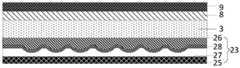
本申请实施例提供了一种微流控器件,如图1所示,所述微流控芯片包括:对盒设置的下基板1和上基板2;An embodiment of the present application provides a microfluidic device. As shown in FIG. 1 , the microfluidic chip includes: a
所述下基板1包括:下衬底基板3,位于所述下衬底基板3面向所述上基板2一侧的容纳液滴的微流道4;The
所述上基板2包括:上衬底基板5,位于所述上衬底基板5面向所述下基板1一侧的多个电极组6,位于所述电极组6面向所述下基板1一侧的介质层7;The
所述电极组6的正投影落入所述微流道4的正投影内;The orthographic projection of the
所述电极组6被配置为:对所述电极组6施加电压,以使所述介质层7发生可逆介电击穿。The
需要说明的是,本申请实施例提供的微流控器件,对电极组施加电压以使介质层发生介电击穿,该介电击穿属于电击穿,是一种可逆的非破坏性的介电击穿。介质层在未发生介电击穿时为绝缘体,发生介电击穿则变为导体,并且,需要混匀的样品液滴通常包括可电解的电解液,当介质层发生介电击穿,液滴电解会产生气泡,从而可以利用气泡的搅拌效应实现待混匀样品的快速、高通量可控主动混匀。It should be noted that, in the microfluidic device provided in the embodiments of the present application, a voltage is applied to the electrode group to cause dielectric breakdown of the dielectric layer, and the dielectric breakdown belongs to electrical breakdown, which is a reversible non-destructive Dielectric breakdown. The dielectric layer is an insulator when no dielectric breakdown occurs, and becomes a conductor when dielectric breakdown occurs. Moreover, the sample droplets that need to be mixed usually include an electrolyzable electrolyte. When dielectric breakdown occurs in the dielectric layer, the liquid Drop electrolysis will generate bubbles, so that the stirring effect of bubbles can be used to realize fast, high-throughput controllable active mixing of samples to be mixed.
本申请实施例提供的微流控器件,由于在上基板设置有介质层以及电极组,对电极组施加电压可以使得介质层发生可逆介电击穿,从而可以使得在微流道内待混匀样品的液滴电解产生气泡,利用气泡的搅拌效应实现了样品的快速混匀,提高在微流控器件内进行样品混匀的效率,从而提高微流控器件检测效率。In the microfluidic device provided by the embodiments of the present application, since the upper substrate is provided with a dielectric layer and an electrode group, applying a voltage to the electrode group can cause reversible dielectric breakdown of the dielectric layer, so that the sample to be mixed in the microfluidic channel can be homogeneously The droplet electrolysis generates bubbles, and the stirring effect of the bubbles is used to realize the rapid mixing of the sample, which improves the efficiency of sample mixing in the microfluidic device, thereby improving the detection efficiency of the microfluidic device.
需要说明的是,图1中,填充微流道4的物质包括待混匀液滴17和驱动液29。It should be noted that, in FIG. 1 , the substances filling the
可选地,所述电极组还被配置为:对所述电极组施加电压,以使液滴移动。本申请实施例提供的微流控器件,既包括微流道又包括电极组,即将微流道式的微流控器件与数字微流控器件相结合,可以利用驱动液来驱动液滴移动,也可以利用电极组控制液滴移动,使微流控器件同时具有了流道式微流控器件操控效率高、液滴操控通量大以及数字微流控器件操控精度高的优点。Optionally, the electrode group is further configured to apply a voltage to the electrode group to move the droplet. The microfluidic device provided by the embodiment of the present application includes both a microfluidic channel and an electrode group, that is, a microfluidic device with a microfluidic channel type is combined with a digital microfluidic device, and a driving liquid can be used to drive the droplet to move, The electrode group can also be used to control the movement of the droplets, so that the microfluidic device has the advantages of high control efficiency of the flow channel microfluidic device, large droplet control flux, and high control precision of the digital microfluidic device.
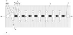
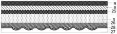
可选地,如图2、图3所示,所述微流道包括:沿第一方向延伸的主流道11,以及与所述主流道11交汇的多对支流道12;Optionally, as shown in FIG. 2 and FIG. 3 , the micro flow channel includes: a
每一对所述支流道12包括:分别位于所述主流道11两侧的第一支流道13和第二支流道14;Each pair of the
所述电极组6的正投影落入所述主流道11的正投影内。The orthographic projection of the
电极组的正投影落入所述主流道的正投影内,即进行样品混匀是在主流道区域完成的。The orthographic projection of the electrode group falls into the orthographic projection of the main channel, that is, the sample mixing is completed in the main channel area.
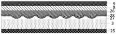
可选地,如图3、图4所示,所述上基板2还包括:贯穿所述上衬底基板的第一入液孔18、多个第二入液孔19、多个第三入液孔20、以及出液孔21;Optionally, as shown in FIG. 3 and FIG. 4 , the
在所述下衬底基板3上,所述第一入液孔18的正投影在所述主流道11的起点区域与所述主流道11的正投影有交叠,所述出液孔21在所述主流道11的终点区域与所述主流道11的正投影有交叠,所述第二入液孔19的正投影在所述第一支流道13的起点区域与所述第一支流道13的正投影有交叠;所述第三入液孔20的正投影在所述第二支流道14的起点区域与所述第二支流道14的正投影有交叠。On the
需要说明的是,图2为微流道在下衬底基板的投影图,图3为微流道、各入液孔和出液孔、以及电极组在下衬底基板的投影图,图4为各入液孔和出液孔、以及电极组在上衬底基板的投影图。图1例如可以是沿图3中AA’的截面图。本申请实施例提供的如图2~4所示的微流控器件,以主流道和支流道均为条形且每对支流道和主流道互相垂直为例进行举例说明,微流控器件包括八对支流道以及八个电极组,在具体实施时,主流道和支流道的形状以及交汇方式可以根据实际需要进行选择,支流道的对数以及电极组的个数也可以根据实际需要进行具体设置。图3、图4中,第一入液孔和出液孔的直径相等,第二入液孔和第三入液孔的直径相等,第一入液孔和第二入液孔的直径不相等,在具体实施时,也可以设置为第一入液孔、第二入液孔、第三入液孔以及第三入液孔的直径均相等。第一入液孔、第二入液孔、第三入液孔以及第三入液孔的直径可以根据实际需要进行选择。It should be noted that FIG. 2 is a projection view of the microfluidic channel on the lower substrate, FIG. 3 is a projection view of the microfluidic channel, each liquid inlet hole and liquid outlet hole, and the electrode group on the lower substrate substrate, and FIG. 4 is each Projection of the liquid inlet and outlet holes, and the electrode group on the upper substrate. Figure 1 may be, for example, a cross-sectional view along AA' in Figure 3 . The microfluidic device shown in FIGS. 2 to 4 provided in the embodiment of the present application is illustrated by taking the main flow channel and the branch flow channel as strips, and each pair of the branch flow channel and the main flow channel are perpendicular to each other. The microfluidic device includes: Eight pairs of branch channels and eight electrode groups, in the specific implementation, the shape and intersection of the main channel and the branch channel can be selected according to actual needs, the number of pairs of branch channels and the number of electrode groups can also be specified according to actual needs. set up. In Figure 3 and Figure 4, the diameters of the first liquid inlet hole and the liquid outlet hole are equal, the diameter of the second liquid inlet hole and the third liquid inlet hole are equal, and the diameters of the first liquid inlet hole and the second liquid inlet hole are not equal , in the specific implementation, it can also be set that the diameters of the first liquid inlet hole, the second liquid inlet hole, the third liquid inlet hole and the third liquid inlet hole are all equal. The diameters of the first liquid inlet hole, the second liquid inlet hole, the third liquid inlet hole and the third liquid inlet hole can be selected according to actual needs.
在利用本申请实施例提供的微流道器件进行样品混匀时,可以在对应于主流道的第一入液孔通入驱动液,在第二入液孔通入第一样品的液滴,在第三入液孔通入第二样品的液滴,第一样品的液滴和第二样品的液滴在主流道汇合,得到待混匀液滴,并在驱动液的驱动下沿主流道流动,当液滴移动到电极组的区域可以对电极组通电,控制液滴移动以使液滴中心与第二子电极中心位于同一直线,之后在对电极组施加电压以使介质层产生可逆介电击穿,介质层由绝缘体变成导体,待混匀液滴中的电解液电解产生气泡,从而可以实现待混匀液滴中第一样品和第二样品快速混匀。When using the microfluidic device provided in the embodiment of the present application for sample mixing, the driving liquid can be passed through the first liquid inlet hole corresponding to the main flow channel, and the droplets of the first sample can be passed through the second liquid inlet hole , the droplets of the second sample are passed into the third liquid inlet hole, the droplets of the first sample and the droplets of the second sample are merged in the main channel to obtain the droplets to be mixed, and driven by the driving liquid The main channel flows, when the droplet moves to the area of the electrode group, the electrode group can be energized, and the droplet movement is controlled so that the center of the droplet and the center of the second sub-electrode are on the same line, and then a voltage is applied to the electrode group to generate the dielectric layer. Reversible dielectric breakdown, the dielectric layer changes from an insulator to a conductor, and the electrolyte in the droplet to be mixed is electrolyzed to generate bubbles, so that the first sample and the second sample in the droplet to be mixed can be quickly mixed.
可选地,如图4所示,所述电极组6的数量等于所述支流道12的对数,且每一所述电极组6位于一对所述支流道12远离所述第一入液孔18的一侧。Optionally, as shown in FIG. 4 , the number of the
从而可以保证待混匀样品汇合得到待混匀液滴之后,再使介质层产生可逆介电击穿。Therefore, it can be ensured that after the samples to be mixed are confluent to obtain the droplets to be mixed, reversible dielectric breakdown of the dielectric layer can be generated.
可选地,如图1、图3、图4所示,每一所述电极组6包括沿第一方向X排列的两个所述第一子电极15,以及位于两个所述第一子电极15之间的一个第二子电极16;所述第一方向X为所述主流道11延伸的方向。Optionally, as shown in FIG. 1 , FIG. 3 , and FIG. 4 , each of the
可选地,如图1、图3所示,在第一方向X上,所述第二子电极16的宽度大于所述第一子电极15的宽度。Optionally, as shown in FIGS. 1 and 3 , in the first direction X, the width of the
可选地,如图1所示,在第一方向X上,所述第一子电极15的宽度和所述第二子电极16的宽度均小于所述液滴17的直径;且在第一方向X上,当所述液滴17中心的正投影与所述第二子电极16的中心的正投影重合时,所述液滴17的正投影与两个所述第一子电极15的正投影均有交叠。Optionally, as shown in FIG. 1 , in the first direction X, the width of the
需要说明的是,当待混匀液滴仅覆盖第二子电极时,仅被第二子电极覆盖区域的介质层两侧的电势差相对较小,容易出现电势差无法达到介质层点击穿临界电压的情况,从而该区域介质层无法发生可逆介电击穿,待混匀液滴也不会电解产生气泡。本申请实施例提供的微流控器件,电极组中各电极的尺寸设计考虑了液滴的直径,使需要混匀的样品的液滴的中心正投影与第二子电极中心正投影重合时,液滴还覆盖第一子电极的区域,从而可以确保液滴覆盖区域的介质层发生点击穿,使液滴电解产生气泡以实现样品混匀。It should be noted that when the droplet to be mixed only covers the second sub-electrode, the potential difference between the two sides of the dielectric layer in the area only covered by the second sub-electrode is relatively small, and it is easy to occur that the potential difference cannot reach the breakdown critical voltage of the dielectric layer. Therefore, the dielectric layer in this region cannot undergo reversible dielectric breakdown, and the droplets to be mixed will not be electrolyzed to generate bubbles. In the microfluidic device provided by the embodiments of the present application, the size of each electrode in the electrode group is designed considering the diameter of the droplet, so that when the center orthographic projection of the droplet of the sample to be mixed is coincident with the center orthographic projection of the second sub-electrode, The droplet also covers the area of the first sub-electrode, so that the dielectric layer in the area covered by the droplet can be ensured to tap through, so that the droplet is electrolyzed to generate air bubbles to achieve sample mixing.
可选地,如图4所示,所述电极组6的数量等于所述支流道12的对数,且每一所述电极组6位于一对所述支流道12远离所述第一入液孔18的一侧。Optionally, as shown in FIG. 4 , the number of the
具体实施时,微流道的深度例如可以是100微米(μm),主流道的宽度例如可以是300μm,支流道的宽度例如可以是210μm。第一入液孔、第二入液孔、第三入液孔以及出液孔的直径可以相同,第一入液孔、第二入液孔、第三入液孔以及出液孔的可以大于微流道的宽度,第一入液孔、第二入液孔、第三入液孔以及出液孔的直径例如可以是600μm。第二子电极的形状例如可以是正方形,第二子电极的长宽例如可以是300μm,第二子电极的长边尺寸例如可以是300μm,短边尺寸例如可以是100μm,第一子电极和第二子电极之间的间距例如可以是5μm,第一子电极和第二子电极的厚度例如可以是300纳米(nm)。介质层的厚度例如可以是1.5μm。电极组的材料例如可以包括金属。介质层的材料例如可以包括树脂。In a specific implementation, the depth of the micro channel may be, for example, 100 micrometers (μm), the width of the main channel may be, for example, 300 μm, and the width of the branch channel may be, for example, 210 μm. The diameters of the first liquid inlet hole, the second liquid inlet hole, the third liquid inlet hole and the liquid outlet hole can be the same, and the diameters of the first liquid inlet hole, the second liquid inlet hole, the third liquid inlet hole and the liquid outlet hole can be larger than The width of the microchannel, the diameters of the first liquid inlet hole, the second liquid inlet hole, the third liquid inlet hole and the liquid outlet hole can be, for example, 600 μm. The shape of the second sub-electrode may be, for example, a square, the length and width of the second sub-electrode may be, for example, 300 μm, the length of the long side of the second sub-electrode may be, for example, 300 μm, and the size of the short side may be, for example, 100 μm. The distance between the two sub-electrodes may be, for example, 5 μm, and the thickness of the first sub-electrode and the second sub-electrode may be, for example, 300 nanometers (nm). The thickness of the dielectric layer may be, for example, 1.5 μm. The material of the electrode group may include metal, for example. The material of the dielectric layer may include resin, for example.
可选地,如图1所示,所述下基板1还包括:位于所述下衬底基板3面向所述上基板2一侧且位于所述微流道内的第一电极层8;所述第一电极层至少位于所述主流道内。Optionally, as shown in FIG. 1 , the
需要说明的是,介质层发生电击穿需要使介质层两侧的电势差不小于其电击穿临界值。当仅利用电极组实现介质层可逆介电击穿时,需要对第二子电极施加较大的电压,对微流控器件的供电电源要求较高。而本申请实施例提供的微流控器件,由于下基板还设置有第一电极层,第一电极层和电极组分别位于介质层两侧,从而可以通过第一电极层和电极组在介质层两侧形成容易使介质层发生可逆介电击穿的电场。更容易实现对介质层可逆介电击穿范围的调控。It should be noted that, the electrical breakdown of the dielectric layer requires that the potential difference on both sides of the dielectric layer be not less than its electrical breakdown critical value. When only the electrode group is used to realize the reversible dielectric breakdown of the dielectric layer, a large voltage needs to be applied to the second sub-electrode, which requires a high power supply for the microfluidic device. However, in the microfluidic device provided by the embodiment of the present application, since the lower substrate is further provided with a first electrode layer, the first electrode layer and the electrode group are respectively located on both sides of the dielectric layer, so that the first electrode layer and the electrode group can be connected to the dielectric layer through the first electrode layer and the electrode group. An electric field is formed on both sides to easily cause reversible dielectric breakdown of the dielectric layer. It is easier to control the reversible dielectric breakdown range of the dielectric layer.
可选地,所述微流控器件还包括与所述第一电极层电连接的地电极;所述微流控器件还包括:与所述电极组电连接的驱动芯片。Optionally, the microfluidic device further includes a ground electrode electrically connected to the first electrode layer; the microfluidic device further includes: a driving chip electrically connected to the electrode group.
如图1所示,本申请实施例提供的微流控器件,下基板1还包括第一疏水层9,上基板2还包括第二疏水层10。As shown in FIG. 1 , in the microfluidic device provided by the embodiment of the present application, the
具体实施时,第一电极层的厚度例如可以是300nm,第一疏水层和第二疏水层的厚度例如可以是60nm。In a specific implementation, the thickness of the first electrode layer may be, for example, 300 nm, and the thickness of the first hydrophobic layer and the second hydrophobic layer may be, for example, 60 nm.
在具体实施时,对于下基板的制备,例如可以对下衬底基板进行图形化工艺在下衬底基板上形成微流道的图案,之后在微流道内依次形成第一电极层、第一疏水层。对于上基板的制备,例如可以在上衬底基板上形成电极组,之后依次形成介质层、第二疏水层,再之后形成第一入液孔、第二入液孔、第三入液孔以及出液孔。将制备完成的上基板和下基板对盒形成本申请实施例提供的微流控器件。In specific implementation, for the preparation of the lower substrate, for example, a patterning process may be performed on the lower substrate to form a pattern of micro-channels on the lower substrate, and then a first electrode layer and a first hydrophobic layer are sequentially formed in the micro-channel . For the preparation of the upper substrate, for example, an electrode group can be formed on the upper substrate substrate, and then a dielectric layer, a second hydrophobic layer are formed in sequence, and then a first liquid inlet hole, a second liquid inlet hole, a third liquid inlet hole and Outlet hole. The prepared upper substrate and lower substrate are assembled into boxes to form the microfluidic device provided in the embodiments of the present application.
需要说明的是,现有技术提供的微流控器件,当完成样品自动制备、混匀、操控后,需要对样品进行检测时,一般需要借助分离的外界设备如显微镜、光谱仪等,不利于微流控器件集成化发展。一般生物检测光学系统大都是由复杂的空间光学元器件搭建而成,其中包括:光源、光束准直透镜、激发滤光片、二向色镜和发射滤光片等,光学检测系统的体积较大,且光路光程较长,需要较强的激发光强来抵消光强衰减,且需提高探测器灵敏度收集较小检测信号。这样复杂的设计在一定程度上增加了产品精细程度要求、提高了工艺制作的难度、增加了硬件复杂度和制作成本。It should be noted that the microfluidic device provided by the prior art generally requires the use of separate external equipment such as microscopes, spectrometers, etc., when the sample needs to be tested after the automatic preparation, mixing and manipulation of the sample is completed, which is not conducive to the microfluidic device. The development of integrated flow control devices. Generally, biological detection optical systems are mostly constructed of complex spatial optical components, including: light source, beam collimating lens, excitation filter, dichroic mirror and emission filter, etc. The volume of the optical detection system is relatively large. It needs a large excitation light intensity to offset the attenuation of the light intensity, and the detector sensitivity needs to be improved to collect smaller detection signals. Such a complex design increases the requirements for the fineness of the product to a certain extent, increases the difficulty of process manufacturing, and increases the hardware complexity and manufacturing cost.
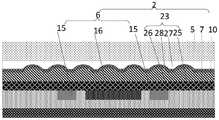
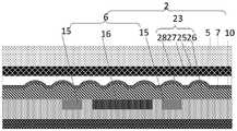
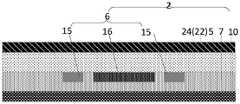
可选地,如图5~图25所示,所述微流控器件还包括:在垂直于所述微流控器件所在平面方向上,分别位于所述微流道4两侧的第一光学组件22和第二光学组件23;Optionally, as shown in FIGS. 5 to 25 , the microfluidic device further includes: in a direction perpendicular to the plane where the microfluidic device is located, first optical optics located on both sides of the
所述第一光学组件22包括:第一滤光片24;The first
所述第二光学组件23包括:第二滤光片25,位于所述第二滤光片25任一侧的微透镜阵列(Micro lens)26,位于所述微透镜阵列26入光侧的准直平坦化层27;The second
所述第一光学组件22的正投影和所述第二光学组件23的正投影至少覆盖所述微流道4。The orthographic projection of the first
需要说明的是,当对本申请实施例提供的微流控器件中的样品进行检测时,还需要设置光源以及光电探测器,光源和探测器分别位于微流控器件两侧,光源发出的激发光束照射样品发出荧光,样品发出的荧光到达光电探测器以实现对样品的检测。本申请实施例提供的微流控器件中,准直平坦化层和微透镜阵列将光源发射出来的光进行整形准直。第二滤光片仅使光源发出的激发光能够有效的通过,而避免外界荧光波段的光线进入微流控器件。第一滤光片进一步过滤掉激发光以及其他杂散光,使得探测器可以获得更纯粹的荧光信号。It should be noted that, when the samples in the microfluidic device provided in the embodiments of the present application are detected, a light source and a photodetector also need to be set. The irradiated sample emits fluorescence, and the fluorescence emitted by the sample reaches the photodetector to realize the detection of the sample. In the microfluidic device provided by the embodiment of the present application, the collimation and flattening layer and the microlens array shape and collimate the light emitted by the light source. The second filter only enables the excitation light emitted by the light source to pass effectively, and prevents the light in the external fluorescence band from entering the microfluidic device. The first filter further filters out excitation light and other stray light, so that the detector can obtain a purer fluorescence signal.
本申请实施例提供的微流控器件,将对样品进行光学检测的除光源以及光电探测器以外的光学组件设置在微流控器件内,即光学组件与微流控器件集成,在可以微流控器件实现样品快速混匀的情况下,进一步提升了微流控器件的集成度,进一步增加了微流控器件的用途,并且无需进行复杂的光学对位,可以有效缩短光程,还可以减小光学检测系统的体积。并且由于第一滤光层和第二滤光层位于微流控器件内部,第一滤光层和第二滤光层距离待测样品的距离较近,通过第二滤光片的激发光经过较短的光程照射与样品,提高照射到样品的激发光光强,激发光通带较窄。而第一滤光层设置在微流控器件内,从而可以大大减小光电探测器与微流控器件的距离,光电探测器接收较强的荧光信号,可以提高检测信号的强度,从而提高检测准确率。In the microfluidic device provided in the embodiment of the present application, the optical components other than the light source and the photodetector for optically detecting the sample are arranged in the microfluidic device, that is, the optical component is integrated with the microfluidic device, and the microfluidic device can be used in the microfluidic device. In the case of controlling the device to realize the rapid mixing of the sample, the integration degree of the microfluidic device is further improved, and the use of the microfluidic device is further increased, and complex optical alignment is not required, which can effectively shorten the optical path and reduce the Small optical detection system volume. And because the first filter layer and the second filter layer are located inside the microfluidic device, the distance between the first filter layer and the second filter layer is relatively close to the sample to be tested, and the excitation light passing through the second filter passes through the microfluidic device. The shorter optical path irradiates the sample, increases the intensity of the excitation light irradiated to the sample, and the excitation light passband is narrower. The first filter layer is arranged in the microfluidic device, so that the distance between the photodetector and the microfluidic device can be greatly reduced. The photodetector receives a strong fluorescent signal, which can improve the intensity of the detection signal, thereby improving detection. Accuracy.
可选地,如图5所示,所述第二光学组件23还包括:位于所述微透镜阵列26和所述准直平坦化层27之间的抗反射层28。Optionally, as shown in FIG. 5 , the second
本申请实施例提供的微流控器件,在准直平坦化层和微透镜阵列之间还设置有抗反射层,从而可以减少光到达不同截面产生的反射,减少光损失,提高照射到样品的光信号的强度,进而提高样品发车的荧光信号的强度,提高检测准确率。In the microfluidic device provided by the embodiment of the present application, an anti-reflection layer is further arranged between the collimation and flattening layer and the microlens array, so that the reflection caused by the light reaching different sections can be reduced, the light loss can be reduced, and the irradiated sample to the sample can be improved. The intensity of the light signal, thereby improving the intensity of the fluorescent signal emitted by the sample, and improving the detection accuracy.
当微流控器件包括第一光学组件和第二光学组件时,上衬底基板、下衬底基板、电极组、介质层、第一疏水层、第二疏水层以及第一电极层的材料为透明材料。电极组以及第一电极层的材料例如可以是氧化铟锡(ITO)。准直平坦化层和抗反射层例如可以选择折射率较低的光学透明材料,折射率例如可以是1.2~1.4,例如可以选择低折射率的聚硅氧烷材料,准直平坦化层和抗反射层的厚度例如可以是微米级别。Micro lens可以选择高折射率光学透明材料,折射率例如可以是1.7~1.8,如高折射率的聚硅氧烷材料,其厚度例如可以是微米级别。第一滤光层和第二滤光层滤光波段不同,第一滤光层和第二滤光层的材料可在下列材料中选择:氧化硅(SiO2)、氧化钛(TiO2)、银(Ag)、铝(Al),第一滤光层和第二滤光层的厚度例如可以是纳米级。When the microfluidic device includes the first optical component and the second optical component, the materials of the upper substrate substrate, the lower substrate substrate, the electrode group, the medium layer, the first hydrophobic layer, the second hydrophobic layer and the first electrode layer are: Transparent material. The material of the electrode group and the first electrode layer can be, for example, indium tin oxide (ITO). For example, the collimation and planarization layer and the anti-reflection layer can be selected from optically transparent materials with a lower refractive index, and the refractive index can be, for example, 1.2 to 1.4. The thickness of the reflective layer may be, for example, in the order of micrometers. For the Micro lens, a high-refractive-index optically transparent material can be selected, for example, the refractive index can be 1.7-1.8, such as a high-refractive-index polysiloxane material, and its thickness can be, for example, in the order of micrometers. The first filter layer and the second filter layer have different filter bands, and the materials of the first filter layer and the second filter layer can be selected from the following materials: silicon oxide (SiO2 ), titanium oxide (TiO2 ), The thicknesses of silver (Ag), aluminum (Al), the first filter layer and the second filter layer may be, for example, nanoscale.
需要说明的是,第一光学组件设置在靠近光电探测器的基板,第二光学组件设置在靠近光源的基板。例如当光电探测器位于下基板背离上基板的一侧时,下基板包括第一光学组件,上基板包括第二光学组件,相反的,当光电探测器位于上基板背离下基板的一侧时,上基板包括第一光学组件,下基板包括第二光学组件。It should be noted that the first optical assembly is disposed on the substrate close to the photodetector, and the second optical assembly is disposed on the substrate close to the light source. For example, when the photodetector is located on the side of the lower substrate away from the upper substrate, the lower substrate includes the first optical component, and the upper substrate includes the second optical component. On the contrary, when the photodetector is located on the side of the upper substrate away from the lower substrate, The upper substrate includes a first optical component, and the lower substrate includes a second optical component.
当下基板包括第一光学组件时,可选地,如图5所示,所述第一光学组件22位于所述第一电极层8背离所述下衬底基板3一侧;或者,如图6所示,所述第一光学组件22位于所述下衬底基板3和所述第一电极层8之间;或者,如图7所示,所述第一光学组件22位于所述下衬底基板3背离所述上衬底基板5一侧;需要说明的是,图6、图7中未示出微流道。When the lower substrate includes a first optical component, optionally, as shown in FIG. 5 , the first
当上基板包括第二光学组件时,可选地,如图5、图8所示,所述第二光学组件23位于所述上衬底基板5背离所述下衬底基板3一侧;When the upper substrate includes a second optical component, optionally, as shown in FIG. 5 and FIG. 8 , the second
或者,如图9、图10所示,所述第二光学组件23位于所述上衬底基板5和所述电极组6之间;Alternatively, as shown in FIG. 9 and FIG. 10 , the second
或者,所述第二光学组件位于所述电极组背离所述下基板的一侧,且所述上衬底基板位于所述第二滤光片和所述微透镜阵列之间;如图11所示,所述第二滤光片25位于所述上衬底基板5和所述电极组6之间,所述微透镜阵列26位于所述上衬底基板5背离所述第二滤光片25一侧;如图12所示,所述微透镜阵列26位于所述上衬底基板5和所述电极组6之间,所述准直平坦化层27位于所述微透镜阵列26与所述上衬底基板5之间,所述第二滤光片25位于所述上衬底基板5背离所述微透镜阵列26一侧。Alternatively, the second optical component is located on the side of the electrode group away from the lower substrate, and the upper substrate is located between the second filter and the microlens array; as shown in FIG. 11 As shown, the
当下基板包括第一光学组件时且上基板包括第二光学组件,图5~图7中的下基板可以与图5、图8~图12中的上基板自由组合。其中,图8、图10、图12中,第二滤光片位于微透镜阵列的入光侧,图5、图9、图11中,第二滤光片位于微透镜阵列的出光侧。When the lower substrate includes the first optical component and the upper substrate includes the second optical component, the lower substrate in FIGS. 5 to 7 can be freely combined with the upper substrate in FIGS. 5 and 8 to 12 . 8 , 10 and 12 , the second filter is located on the light-incident side of the microlens array, and in FIGS. 5 , 9 and 11 , the second filter is located on the light-exit side of the microlens array.
本申请实施例提供的如图5所示的微流控器件,相比于其他方案,第一滤光片更接近微流道,从而第一滤光片更接近待测样品,从而可以使得光电探测器接收较强的荧光信号,可以提高检测信号的强度,从而提高检测准确率。In the microfluidic device shown in FIG. 5 provided in the embodiment of the present application, compared with other solutions, the first optical filter is closer to the microfluidic channel, so that the first optical filter is closer to the sample to be tested, so that the optoelectronic The detector receives a strong fluorescent signal, which can improve the intensity of the detection signal, thereby improving the detection accuracy.
当上基板包括第一光学组件时,可选地,如图13所示,所述第一光学组件22位于所述上衬底基板5和所述电极组6之间;或者,如图14所示,所述第一光学组件22位于所述上衬底基板5背离所述下衬底基板3一侧。When the upper substrate includes a first optical component, optionally, as shown in FIG. 13 , the first
本申请实施例提供的如图13所示的微流控器件,第一滤光片更接近微流道,从而第一滤光片更接近待测样品,从而可以使得光电探测器接收较强的荧光信号,可以提高检测信号的强度,从而提高检测准确率。In the microfluidic device shown in FIG. 13 provided by the embodiment of the present application, the first filter is closer to the microchannel, so that the first filter is closer to the sample to be tested, so that the photodetector can receive strong The fluorescence signal can improve the intensity of the detection signal, thereby improving the detection accuracy.
当下基板包括第二光学组件时,可选地,如图13、图15所示,所述第二光学组件23位于所述下衬底基板3背离所述上衬底基板5一侧;When the lower substrate includes a second optical component, optionally, as shown in FIG. 13 and FIG. 15 , the second
或者,所述第二光学组件位于所述下衬底基板面向所述上衬底基板一侧;如图16、图17所示,所述第二光学组件23位于所述下衬底基板3和所述第一电极层8之间;如图18、图19,第二光学组件23位于第一电极层8和第一疏水层9之间;如图20所示,第二滤光片25位于第一电极层8和第一疏水层9之间,微透镜阵列26位于第一电极层8和下衬底基板3之间,准直平坦化层27位于微透镜阵列26和下衬底基板3之间;如图21所示,微透镜阵列26位于第一电极层8和第一疏水层9之间,准直平坦化层27位于微透镜阵列26和第一电极层8之间,第二滤光片25位于第一电极层8和下衬底基板3之间;Alternatively, the second optical component is located on the side of the lower substrate facing the upper substrate; as shown in FIG. 16 and FIG. 17 , the second
或者,所述下衬底基板位于所述微透镜阵列和所述第二滤光片之间;如图22所示,第二滤光片25位于下衬底基板3和第一电极层8之间,微透镜阵列26位于下衬底基板3背离第一电极层8一侧;如图23所示,微透镜阵列26位于下衬底基板3和第一电极层8之间,准直平坦化层27位于微透镜阵列26和下衬底基板3之间,第二滤光片25位于下衬底基板3背离第一电极层8一侧;如图24所示,第二滤光片25位于第一电极层8和第一疏水层9之间,微透镜阵列26位于下衬底基板3背离第一电极层8一侧;如图25所示,第二滤光片25位于第一电极层8和第一疏水层9之间,微透镜阵列26位于下衬底基板3背离第一电极层8一侧。Alternatively, the lower substrate is located between the microlens array and the second filter; as shown in FIG. 22 , the
图13、图15~图25中未示出微流道。The microfluidic channel is not shown in FIGS. 13 and 15 to 25 .
当上基板包括第一光学组件且下基板包括第二光学组件时,图13~图14中的上基板可以与图13、图15~图25中的下基板自由组合。其中,图15、图16、图19、图21、图23、图25中,第二滤光片位于微透镜阵列的入光侧,图13、图17、图18、图20、图22、图24中,第二滤光片位于微透镜阵列的出光侧。When the upper substrate includes the first optical component and the lower substrate includes the second optical component, the upper substrate in FIGS. 13 to 14 can be freely combined with the lower substrate in FIGS. 13 and 15 to 25 . 15, 16, 19, 21, 23, and 25, the second filter is located on the light-incident side of the microlens array. In FIG. 24, the second filter is located on the light-emitting side of the microlens array.
基于同一发明构思,本申请实施例还提供的一种利用上述微流控器件进行样品混匀的方法,如图26所示,所述方法包括:Based on the same inventive concept, an embodiment of the present application also provides a method for mixing samples using the above-mentioned microfluidic device, as shown in FIG. 26 , the method includes:
S101、第一阶段,向所述微流道通入驱动液、待混匀的第一样品和第二样品,以及利用所述驱动液驱动所述第一样品和所述第二样品组成的待混匀液滴向所述电极组移动;S101. In the first stage, a driving liquid, a first sample and a second sample to be mixed are introduced into the microfluidic channel, and the driving liquid is used to drive the first sample and the second sample to form a composition The droplets to be mixed move toward the electrode group;
S102、第二阶段,当所述待混匀液滴的正投影与所述电极组的正投影有交叠时,对所述电极组加载电压,驱动所述待混匀液滴移动;S102. In the second stage, when the orthographic projection of the droplet to be mixed overlaps with the orthographic projection of the electrode group, a voltage is applied to the electrode group to drive the droplet to be mixed to move;
S103、第三阶段,当所述待混匀液滴与所述电极组的中心重合时,并停止通入所述驱动液,调节对所述电极组加载的电压,以使所述介质层产生可逆介电击穿,并使得所述待混匀液滴电解产生气泡,以使所述待混匀液滴中的所述第一样品和所述第二样品混匀。S103. In the third stage, when the droplet to be mixed is coincident with the center of the electrode group, the driving liquid is stopped, and the voltage applied to the electrode group is adjusted to make the dielectric layer generate Reversible dielectric breakdown and electrolysis of the droplets to be mixed to generate bubbles, so as to mix the first sample and the second sample in the droplets to be mixed.
本申请实施例提供的样品混匀方法,在微流控器件中进行,首先利用驱动液驱动待混匀液滴向电极组移动,之后当液滴移动到电极组覆盖的区域时,利用电极组驱动待混匀液滴与电极组中心重合,之后再对电极组施加电压以使得介质层发生可逆介电击穿,从而可以使得在微流道内待混匀样品的液滴电解产生气泡,利用气泡的搅拌效应实现了样品的快速混匀,提高在微流控器件内进行样品混匀的效率,从而提高微流控器件检测效率。并且,本申请实施例提供的样品混匀方法将微流道式利用驱动液来驱动液滴移动的方式与数字微流控式对液滴驱动的方式相结合,使其同时具有了流道式微流控器件操控效率高、液滴操控通量大以及数字微流控器件操控精度高的优点。The sample mixing method provided in the embodiment of the present application is carried out in a microfluidic device. First, a driving liquid is used to drive the droplet to be mixed to move toward the electrode group, and then when the droplet moves to the area covered by the electrode group, the electrode group is used The droplet to be mixed is driven to coincide with the center of the electrode group, and then a voltage is applied to the electrode group to cause reversible dielectric breakdown of the dielectric layer, so that the droplet of the sample to be mixed in the microchannel can be electrolyzed to generate bubbles. The stirring effect realizes the rapid mixing of the sample, improves the efficiency of sample mixing in the microfluidic device, and thus improves the detection efficiency of the microfluidic device. In addition, the sample mixing method provided in the embodiment of the present application combines the microfluidic method of using driving fluid to drive droplets to move with the digital microfluidic method of driving droplets, so that it has a channel-type microfluidic method at the same time. The fluidic device has the advantages of high manipulation efficiency, large droplet manipulation flux, and high manipulation accuracy of digital microfluidic devices.
需要说明的是,在选择驱动液时,应保证第一样品和第二样品及其混合溶液不溶于驱动液,通常驱动液例如可以是油或硅油。It should be noted that, when selecting the driving fluid, it should be ensured that the first sample and the second sample and their mixed solutions are insoluble in the driving fluid, usually the driving fluid may be, for example, oil or silicone oil.
可选地,向所述微流道通入驱动液、待混匀的第一样品和第二样品,具体包括:Optionally, the driving fluid, the first sample to be mixed and the second sample to be mixed are introduced into the microfluidic channel, which specifically includes:
向所述主流道持续通入驱动液,在所述驱动液充满所述主流道后,向所述第一支流道通入第一样品以及向所述第二支流道通入第二样品,并持续通入所述驱动液,以使所述第一样品和所述第二样品流至所述支流道与所述主流道交汇区域时与所述支流道分离。The driving fluid is continuously supplied into the main channel, and after the driving fluid fills the main channel, the first sample is supplied to the first branch channel and the second sample is supplied to the second branch channel, The driving fluid is continuously supplied, so that the first sample and the second sample are separated from the branch channel when they flow to the intersection area of the branch channel and the main channel.
即持续通入驱动液并利用其剪切力完成第一样品与第一支流道的分离以及完成第二样品与第二支流道的分离。具体实施时,向所述第一支流道通入第一样品以及向所述第二支流道通入第二样品达到预设体积时,停止通入第一样品和第二样品。That is, the driving fluid is continuously introduced and the shearing force thereof is used to complete the separation of the first sample from the first branch channel and the separation of the second sample from the second branch channel. During specific implementation, when the first sample is introduced into the first branch channel and the second sample is introduced into the second branch channel to reach a preset volume, the first sample and the second sample are stopped.
可选地,当所述待混匀液滴的正投影与所述电极组的正投影有交叠时,对所述电极组加载电压,具体包括:Optionally, when the orthographic projection of the droplet to be mixed overlaps with the orthographic projection of the electrode group, applying a voltage to the electrode group specifically includes:
在所述待混匀液滴的中心的正投影与所述第二子电极中心的正投影重合之前,依次对所述第一子电极和所述第二子电极加载第一电压信号,以使所述待混匀液滴沿所述主流道移动。Before the orthographic projection of the center of the droplet to be mixed coincides with the orthographic projection of the center of the second sub-electrode, a first voltage signal is sequentially applied to the first sub-electrode and the second sub-electrode, so that the The droplets to be mixed move along the main flow channel.
即同时利用介电润湿效应和驱动液对待混匀液滴的推动效应,控制待混匀液滴移动。That is, the movement of the droplets to be mixed is controlled by simultaneously using the dielectric wetting effect and the driving effect of the driving liquid to the droplets to be mixed.
具体实施时,可以对电极组施加30伏(V)的电压。In a specific implementation, a voltage of 30 volts (V) can be applied to the electrode group.
可选地,所述下基板包括第一电极层,所述第一电极层与地电位电连接,当所述待混匀液滴与所述电极组的中心重合时,调节对所述电极组加载的电压,具体包括:Optionally, the lower substrate includes a first electrode layer, and the first electrode layer is electrically connected to the ground potential. When the droplet to be mixed is coincident with the center of the electrode group, the adjustment to the electrode group is adjusted. Loaded voltage, including:
对所述第一子电极加载第二电压信号,以及对所述第二子电极加载第三电压信号,以使所述介质层两侧的电势差不小于所述介质层可逆介电击穿临界电压。A second voltage signal is applied to the first sub-electrode, and a third voltage signal is applied to the second sub-electrode, so that the potential difference on both sides of the dielectric layer is not less than the reversible dielectric breakdown threshold voltage of the dielectric layer .
具体实施时,每种电介质的电击穿临界电压均为固定值,以介质层的材料为树脂为例,对微流控器件的电场分布进行模拟,其中,树脂的电击穿临界电压约为233千伏/厘米(kV/cm)。图27~图28中的线段ab代表第一子电极和第二子电极之间的间距,需要说明的是,图27中线段ab的长度大于图28中线段ab的长度,图27中对应的微流控器件,当待混匀液滴的中心与第二子电极中心的正投影重合时,液滴还覆盖位于第二子电极两侧的第一子电极,而图28中对应的微流控器件,当待混匀液滴的中心与第二子电极中心的正投影重合时,液滴未覆盖第一子电极。图27中线段ab的长度对应的微流控器件的电场分布如图29所示,图28中线段ab的长度对应的微流控器件的电场分布如图30所示。图29~图30中A点和B点代表在垂直于介质层的同一直线上分别位于介质层上、下表面的点。通过模拟可知,如图29所示,介质层两侧的电势差UAB=32V,达到其电击穿的临界值,通过对微流控器件的电场分布的模拟可知,该方案中第三电压信号为60V、第二电压信号为0,第一电极层接地时,介质层两侧的电势差UAB=32V。如图30所示,当待混匀液滴仅覆盖第二子电极时,介质层两侧的电势差UAB相对较小,UAB=20V,无法达到介质层电击穿的临界电压。In the specific implementation, the electrical breakdown threshold voltage of each dielectric is a fixed value. Taking the material of the dielectric layer as resin as an example, the electric field distribution of the microfluidic device is simulated. The electrical breakdown threshold voltage of the resin is about 233 kilovolts per centimeter (kV/cm). The line segment ab in FIGS. 27 to 28 represents the distance between the first sub-electrode and the second sub-electrode. It should be noted that the length of the line segment ab in FIG. 27 is greater than the length of the line segment ab in FIG. In the microfluidic device, when the center of the droplet to be mixed coincides with the orthographic projection of the center of the second sub-electrode, the droplet also covers the first sub-electrodes on both sides of the second sub-electrode, and the corresponding microfluidic device in Figure 28 When the center of the droplet to be mixed coincides with the orthographic projection of the center of the second sub-electrode, the droplet does not cover the first sub-electrode. The electric field distribution of the microfluidic device corresponding to the length of the line segment ab in FIG. 27 is shown in FIG. 29 , and the electric field distribution of the microfluidic device corresponding to the length of the line segment ab in FIG. 28 is shown in FIG. 30 . Points A and B in FIGS. 29 to 30 represent points located on the upper and lower surfaces of the dielectric layer, respectively, on the same line perpendicular to the dielectric layer. It can be seen from the simulation that, as shown in Figure 29, the potential difference between the two sides of the dielectric layer UAB = 32V, which reaches the critical value of its electrical breakdown. The simulation of the electric field distribution of the microfluidic device shows that the third voltage signal in this scheme When the voltage signal is 60V, the second voltage signal is 0, and the first electrode layer is grounded, the potential difference between the two sides of the dielectric layer is UAB =32V. As shown in Figure 30, when the droplet to be mixed only covers the second sub-electrode, the potential difference UAB on both sides of the dielectric layer is relatively small, UAB =20V, which cannot reach the critical voltage of dielectric layer electrical breakdown.
可选地,在所述第三阶段后,所述方法还包括:Optionally, after the third stage, the method further includes:
第四阶段,对所述电极组加载电压预设时长后,停止对所述电极组施加电压,并持续通入所述驱动液,驱动混匀后的液滴从出液口流出。In the fourth stage, after the voltage is applied to the electrode group for a preset period of time, the application of the voltage to the electrode group is stopped, and the driving liquid is continuously supplied to drive the mixed droplets to flow out from the liquid outlet.
接下来以微流控器件包括第一电极层,且第一电极层接地为例,对本申请实施例提供的样品混匀方法进行举例说明。Next, the sample mixing method provided in the embodiment of the present application is illustrated by taking the example that the microfluidic device includes a first electrode layer and the first electrode layer is grounded.
S201、控制电极组断电,向主流道持续通入驱动液,在驱动液充满主流道后,向第一支流道通入第一样品以及向第二支流道通入第二样品,当第一样品以及第二样品达到预设体积时,停止通入第一样品和第二样品,持续通入驱动液,以使第一样品和第二样品流至所述支流道与所述主流道交汇区域时与所述支流道分离,并利用所述驱动液驱动所述第一样品和所述第二样品组成的待混匀液滴向所述电极组移动;S201. Control the power off of the electrode group, and continuously feed the driving fluid into the main channel. After the driving fluid fills the main channel, pass the first sample into the first branch channel and the second sample into the second branch channel. When the first sample and the second sample reach the preset volume, stop feeding the first sample and the second sample, and continue feeding the driving fluid, so that the first sample and the second sample flow to the branch channel and the When the main channel meets the area, it is separated from the branch channel, and the driving liquid is used to drive the droplet to be mixed composed of the first sample and the second sample to move toward the electrode group;
S202、利用驱动液驱动待混匀液滴想电极组移动,当待混匀液滴的正投影与第一子电极的正投影有交叠时,依次对第一子电极和第二子电极加载30V的第一电压信号,以使待混匀液滴沿所述主流道移;S202. Use the driving liquid to drive the droplet to be mixed to move the electrode group, and when the orthographic projection of the droplet to be mixed overlaps with the orthographic projection of the first sub-electrode, load the first sub-electrode and the second sub-electrode sequentially A first voltage signal of 30V, so that the droplets to be mixed move along the main channel;
S203、当待混匀液滴与第二子电极的中心重合时,停止通入驱动液,调节对第一子电极加载0V电压信号,对第二子电极加载60V电压信号,以使介质层产生可逆介电击穿,并使得待混匀液滴电解产生气泡,保持预设时长,以使待混匀液滴中的所述第一样品和所述第二样品混匀;S203. When the center of the droplet to be mixed coincides with the center of the second sub-electrode, stop feeding the driving liquid, adjust the voltage signal of 0V to be applied to the first sub-electrode, and a voltage signal of 60V to be applied to the second sub-electrode, so that the dielectric layer generates Reversible dielectric breakdown and electrolysis of the droplets to be mixed to generate bubbles for a preset period of time, so as to mix the first sample and the second sample in the droplets to be mixed;
S204、对电极组加载电压预设时长后,停止对电极组加载电压,并持续通入驱动液,驱动混匀后的液滴从出液口流出。S204 , after the voltage is applied to the electrode group for a preset time period, the voltage applied to the electrode group is stopped, and the driving liquid is continuously supplied to drive the mixed droplets to flow out from the liquid outlet.
本申请实施例提供的一种微流控系统,所述微流控系统包括本申请实施例提供的上述微流控器件。A microfluidic system provided by the embodiment of the present application includes the microfluidic device provided by the embodiment of the present application.
综上所述,本申请实施例提供的微流控器件、样品混匀方法以及微流控系统,由于在微流控器件的上基板设置有介质层以及电极组,对电极组施加电压可以使得介质层发生可逆介电击穿,从而可以使得在微流道内待混匀样品的液滴电解产生气泡,利用气泡的搅拌效应实现了样品的快速混匀,提高在微流控器件内进行样品混匀的效率,从而提高微流控器件检测效率。并且,本申请实施例提供的微流控器件,将微流道式利用驱动液来驱动液滴移动的方式与数字微流控式对液滴驱动的方式相结合,使其同时具有了流道式微流控器件操控效率高、液滴操控通量大以及数字微流控器件操控精度高的优点。To sum up, in the microfluidic device, the sample mixing method and the microfluidic system provided in the embodiments of the present application, since the upper substrate of the microfluidic device is provided with a dielectric layer and an electrode group, applying a voltage to the electrode group can make the The dielectric layer undergoes reversible dielectric breakdown, so that the droplets of the sample to be mixed in the microfluidic channel can be electrolyzed to generate bubbles, and the stirring effect of the bubbles is used to realize the rapid mixing of the sample, which improves the sample mixing in the microfluidic device. uniform efficiency, thereby improving the detection efficiency of microfluidic devices. In addition, the microfluidic device provided in the embodiment of the present application combines the microfluidic method of using the driving liquid to drive the droplet to move with the digital microfluidic method of driving the droplet, so that it has a flow channel at the same time. Digital microfluidic devices have the advantages of high manipulation efficiency, large droplet manipulation flux, and high manipulation accuracy of digital microfluidic devices.
显然,本领域的技术人员可以对本申请进行各种改动和变型而不脱离本申请的精神和范围。这样,倘若本申请的这些修改和变型属于本申请权利要求及其等同技术的范围之内,则本申请也意图包含这些改动和变型在内。Obviously, those skilled in the art can make various changes and modifications to the present application without departing from the spirit and scope of the present application. Thus, if these modifications and variations of the present application fall within the scope of the claims of the present application and their equivalents, the present application is also intended to include these modifications and variations.
Claims (19)
Translated fromChinesePriority Applications (1)
| Application Number | Priority Date | Filing Date | Title |
|---|---|---|---|
| CN202010337805.0ACN111450907B (en) | 2020-04-26 | 2020-04-26 | Microfluidic device, sample mixing method, and microfluidic system |
Applications Claiming Priority (1)
| Application Number | Priority Date | Filing Date | Title |
|---|---|---|---|
| CN202010337805.0ACN111450907B (en) | 2020-04-26 | 2020-04-26 | Microfluidic device, sample mixing method, and microfluidic system |
Publications (2)
| Publication Number | Publication Date |
|---|---|
| CN111450907A CN111450907A (en) | 2020-07-28 |
| CN111450907Btrue CN111450907B (en) | 2022-06-24 |
Family
ID=71671126
Family Applications (1)
| Application Number | Title | Priority Date | Filing Date |
|---|---|---|---|
| CN202010337805.0AExpired - Fee RelatedCN111450907B (en) | 2020-04-26 | 2020-04-26 | Microfluidic device, sample mixing method, and microfluidic system |
Country Status (1)
| Country | Link |
|---|---|
| CN (1) | CN111450907B (en) |
Families Citing this family (2)
| Publication number | Priority date | Publication date | Assignee | Title |
|---|---|---|---|---|
| CN114887673B (en)* | 2022-04-26 | 2023-06-09 | 浙江大学 | Integrated flow channel digital micro-fluidic chip and preparation method and application thereof |
| CN115722282B (en)* | 2022-11-15 | 2024-07-16 | 上海天马微电子有限公司 | Microfluidic substrate, microfluidic device and driving method thereof |
Citations (8)
| Publication number | Priority date | Publication date | Assignee | Title |
|---|---|---|---|---|
| CN1934451A (en)* | 2004-03-23 | 2007-03-21 | 东丽株式会社 | Method of agitating solution |
| CN101431090A (en)* | 2007-11-05 | 2009-05-13 | 东部高科股份有限公司 | Image sensor and method for manufacturing the same |
| CN101490562B (en)* | 2006-07-10 | 2012-12-19 | 株式会社日立高新技术 | Liquid transfer device |
| CN107425024A (en)* | 2010-07-15 | 2017-12-01 | 索尼公司 | Solid state image pickup device, the manufacture method of solid state image pickup device and electronic equipment |
| CN108160127A (en)* | 2018-01-31 | 2018-06-15 | 中南林业科技大学 | A kind of microfluidic separation chip and production method |
| CN108465491A (en)* | 2018-03-12 | 2018-08-31 | 京东方科技集团股份有限公司 | Micro-fluidic chip, biological monitor and method |
| CN109003992A (en)* | 2017-06-07 | 2018-12-14 | 采钰科技股份有限公司 | Solid-state imaging device |
| CN110681421A (en)* | 2019-10-08 | 2020-01-14 | 江苏奥素液芯生物技术有限公司 | Digital microfluidic system |
- 2020
- 2020-04-26CNCN202010337805.0Apatent/CN111450907B/ennot_activeExpired - Fee Related
Patent Citations (8)
| Publication number | Priority date | Publication date | Assignee | Title |
|---|---|---|---|---|
| CN1934451A (en)* | 2004-03-23 | 2007-03-21 | 东丽株式会社 | Method of agitating solution |
| CN101490562B (en)* | 2006-07-10 | 2012-12-19 | 株式会社日立高新技术 | Liquid transfer device |
| CN101431090A (en)* | 2007-11-05 | 2009-05-13 | 东部高科股份有限公司 | Image sensor and method for manufacturing the same |
| CN107425024A (en)* | 2010-07-15 | 2017-12-01 | 索尼公司 | Solid state image pickup device, the manufacture method of solid state image pickup device and electronic equipment |
| CN109003992A (en)* | 2017-06-07 | 2018-12-14 | 采钰科技股份有限公司 | Solid-state imaging device |
| CN108160127A (en)* | 2018-01-31 | 2018-06-15 | 中南林业科技大学 | A kind of microfluidic separation chip and production method |
| CN108465491A (en)* | 2018-03-12 | 2018-08-31 | 京东方科技集团股份有限公司 | Micro-fluidic chip, biological monitor and method |
| CN110681421A (en)* | 2019-10-08 | 2020-01-14 | 江苏奥素液芯生物技术有限公司 | Digital microfluidic system |
Also Published As
| Publication number | Publication date |
|---|---|
| CN111450907A (en) | 2020-07-28 |
Similar Documents
| Publication | Publication Date | Title |
|---|---|---|
| Yang et al. | Micro-optics for microfluidic analytical applications | |
| US9861984B2 (en) | Microchip and channel structure for the same | |
| US7477384B2 (en) | Device and method for investigating analytes in liquid suspension or solution | |
| EP3501651B1 (en) | Microfluidic routing | |
| EP3164692B1 (en) | Flow cytometry system and method | |
| HK1216552A1 (en) | Systems, apparatus, and methods for sorting particles | |
| CN111450907B (en) | Microfluidic device, sample mixing method, and microfluidic system | |
| CN107850542A (en) | Optical detection device | |
| US9863878B2 (en) | Photometric analysis method and photometric analysis device using microchip, microchip for photometric analysis device, and processing device for photometric analysis | |
| Vyawahare et al. | Sorting droplets into many outlets | |
| DE60221979T2 (en) | ENERGY RADIATION FOR AN ELECTROPHORES SYSTEM | |
| US20200298236A1 (en) | Fluidic apparatus and method | |
| JP6507891B2 (en) | Light guide member, light lead-out member and light lead-out method | |
| US20220016627A1 (en) | Detection of components | |
| TW504491B (en) | Chip-type device for counting/classifying and analyzing the micro-fluid particle and manufacturing method thereof | |
| Yan | Chemical Signal Analysis with Fourier Microfluidics | |
| Ashok | Integration methods for enhanced trapping and spectroscopy in optofluidics | |
| Grad | The Integration of Active Silicon Components in Polymer Microfluidic Devices | |
| Goel | Optobiochips for Microcytometry (PhD thesis, Electrical Engineering, University of Alberta by Sanket Goel-Jan, 2006) |
Legal Events
| Date | Code | Title | Description |
|---|---|---|---|
| PB01 | Publication | ||
| PB01 | Publication | ||
| SE01 | Entry into force of request for substantive examination | ||
| SE01 | Entry into force of request for substantive examination | ||
| GR01 | Patent grant | ||
| GR01 | Patent grant | ||
| CF01 | Termination of patent right due to non-payment of annual fee | Granted publication date:20220624 | |
| CF01 | Termination of patent right due to non-payment of annual fee |