CN111446282B - Display substrate and display device - Google Patents
Display substrate and display deviceDownload PDFInfo
- Publication number
- CN111446282B CN111446282BCN202010352241.8ACN202010352241ACN111446282BCN 111446282 BCN111446282 BCN 111446282BCN 202010352241 ACN202010352241 ACN 202010352241ACN 111446282 BCN111446282 BCN 111446282B
- Authority
- CN
- China
- Prior art keywords
- sub
- pixel
- area
- type
- light
- Prior art date
- Legal status (The legal status is an assumption and is not a legal conclusion. Google has not performed a legal analysis and makes no representation as to the accuracy of the status listed.)
- Active
Links
Images


Classifications
- H—ELECTRICITY
- H10—SEMICONDUCTOR DEVICES; ELECTRIC SOLID-STATE DEVICES NOT OTHERWISE PROVIDED FOR
- H10K—ORGANIC ELECTRIC SOLID-STATE DEVICES
- H10K59/00—Integrated devices, or assemblies of multiple devices, comprising at least one organic light-emitting element covered by group H10K50/00
- H10K59/10—OLED displays
- H10K59/12—Active-matrix OLED [AMOLED] displays
- H10K59/121—Active-matrix OLED [AMOLED] displays characterised by the geometry or disposition of pixel elements
- H10K59/1213—Active-matrix OLED [AMOLED] displays characterised by the geometry or disposition of pixel elements the pixel elements being TFTs
- G—PHYSICS
- G09—EDUCATION; CRYPTOGRAPHY; DISPLAY; ADVERTISING; SEALS
- G09G—ARRANGEMENTS OR CIRCUITS FOR CONTROL OF INDICATING DEVICES USING STATIC MEANS TO PRESENT VARIABLE INFORMATION
- G09G3/00—Control arrangements or circuits, of interest only in connection with visual indicators other than cathode-ray tubes
- G09G3/20—Control arrangements or circuits, of interest only in connection with visual indicators other than cathode-ray tubes for presentation of an assembly of a number of characters, e.g. a page, by composing the assembly by combination of individual elements arranged in a matrix no fixed position being assigned to or needed to be assigned to the individual characters or partial characters
- G09G3/22—Control arrangements or circuits, of interest only in connection with visual indicators other than cathode-ray tubes for presentation of an assembly of a number of characters, e.g. a page, by composing the assembly by combination of individual elements arranged in a matrix no fixed position being assigned to or needed to be assigned to the individual characters or partial characters using controlled light sources
- G09G3/30—Control arrangements or circuits, of interest only in connection with visual indicators other than cathode-ray tubes for presentation of an assembly of a number of characters, e.g. a page, by composing the assembly by combination of individual elements arranged in a matrix no fixed position being assigned to or needed to be assigned to the individual characters or partial characters using controlled light sources using electroluminescent panels
- G09G3/32—Control arrangements or circuits, of interest only in connection with visual indicators other than cathode-ray tubes for presentation of an assembly of a number of characters, e.g. a page, by composing the assembly by combination of individual elements arranged in a matrix no fixed position being assigned to or needed to be assigned to the individual characters or partial characters using controlled light sources using electroluminescent panels semiconductive, e.g. using light-emitting diodes [LED]
- G09G3/3208—Control arrangements or circuits, of interest only in connection with visual indicators other than cathode-ray tubes for presentation of an assembly of a number of characters, e.g. a page, by composing the assembly by combination of individual elements arranged in a matrix no fixed position being assigned to or needed to be assigned to the individual characters or partial characters using controlled light sources using electroluminescent panels semiconductive, e.g. using light-emitting diodes [LED] organic, e.g. using organic light-emitting diodes [OLED]
- H—ELECTRICITY
- H10—SEMICONDUCTOR DEVICES; ELECTRIC SOLID-STATE DEVICES NOT OTHERWISE PROVIDED FOR
- H10K—ORGANIC ELECTRIC SOLID-STATE DEVICES
- H10K59/00—Integrated devices, or assemblies of multiple devices, comprising at least one organic light-emitting element covered by group H10K50/00
- H10K59/10—OLED displays
- H10K59/12—Active-matrix OLED [AMOLED] displays
- H10K59/121—Active-matrix OLED [AMOLED] displays characterised by the geometry or disposition of pixel elements
- H10K59/1216—Active-matrix OLED [AMOLED] displays characterised by the geometry or disposition of pixel elements the pixel elements being capacitors
- H—ELECTRICITY
- H10—SEMICONDUCTOR DEVICES; ELECTRIC SOLID-STATE DEVICES NOT OTHERWISE PROVIDED FOR
- H10K—ORGANIC ELECTRIC SOLID-STATE DEVICES
- H10K59/00—Integrated devices, or assemblies of multiple devices, comprising at least one organic light-emitting element covered by group H10K50/00
- H10K59/10—OLED displays
- H10K59/12—Active-matrix OLED [AMOLED] displays
- H10K59/131—Interconnections, e.g. wiring lines or terminals
Landscapes
- Engineering & Computer Science (AREA)
- Microelectronics & Electronic Packaging (AREA)
- Physics & Mathematics (AREA)
- Geometry (AREA)
- Computer Hardware Design (AREA)
- General Physics & Mathematics (AREA)
- Theoretical Computer Science (AREA)
- Devices For Indicating Variable Information By Combining Individual Elements (AREA)
- Electroluminescent Light Sources (AREA)
Abstract
Translated fromChinese
Description
Translated fromChinese技术领域technical field
本发明属于显示基板技术领域,具体涉及一种显示基板及显示装置。The invention belongs to the technical field of display substrates, and in particular relates to a display substrate and a display device.
背景技术Background technique
当前,为了提高屏下摄像头所在区域的光透过率,保证屏下摄像头的拍照效果,在摄像头的安装区仅保留发光器件,而控制发光器件发光的信号由横向的同行像素电路引出,其走线采用透明的导电材料。然而,这种方法具有较大的局限性,当摄像头尺寸较大或者存在多个摄像头时,透明导线的数量受到了像素纵向尺寸的限制,导致所控制的发光器件数量有限。At present, in order to improve the light transmittance of the area where the under-screen camera is located and ensure the photo-taking effect of the under-screen camera, only the light-emitting device is reserved in the installation area of the camera, and the signal for controlling the light-emitting device to emit light is drawn from the horizontal parallel pixel circuit, and its The wires are made of transparent conductive material. However, this method has great limitations. When the size of the camera is large or there are multiple cameras, the number of transparent wires is limited by the vertical size of the pixel, resulting in a limited number of controlled light-emitting devices.
发明内容SUMMARY OF THE INVENTION
本发明旨在至少解决现有技术中存在的技术问题之一,提供一种显示基板及显示装置。The present invention aims to solve at least one of the technical problems existing in the prior art, and provides a display substrate and a display device.
第一方面,本公开实施例提供一种显示基板,包括基底,所述基底具有包括安装区、环绕所述安装区的过渡区,环绕所述过渡区的显示区;在所述安装区、所述过渡区、所述显示区中均包括子像素区;其中,位于所述过渡区中的所述子像素区至少包括第一类子像素区和第二类子像素区;所述安装区中的子像素区至少包括第三类子像素区;In a first aspect, an embodiment of the present disclosure provides a display substrate, including a base, the base having a mounting area, a transition area surrounding the mounting area, and a display area surrounding the transition area; Both the transition area and the display area include a sub-pixel area; wherein, the sub-pixel area located in the transition area includes at least a first-type sub-pixel area and a second-type sub-pixel area; in the installation area The sub-pixel area includes at least the third type of sub-pixel area;
在所述第一类子像素区中设置有位于所述基底上的像素电路;所述像素电路包括驱动子电路和发光器件;在所述第二类子像素区中设置有位于所述基底上的所述驱动子电路;在所述第三类子像素区中设置有位于所述基底上所述发光器件;A pixel circuit located on the substrate is provided in the first type of sub-pixel region; the pixel circuit includes a driving sub-circuit and a light emitting device; and a pixel circuit located on the substrate is provided in the second type of sub-pixel region the driving sub-circuit; the light-emitting device located on the substrate is arranged in the third type sub-pixel region;
其中,位于所述安装区的第三类子像素区中的所述发光器件,通过信号连接线与位于所述过渡区的第二类子像素区中的所述驱动子电路连接;且不同的所述发光器件所连接的所述信号连接线和所述驱动子电路均不同;至少部分信号连接线在所述基底上的正投影存在重叠。Wherein, the light-emitting device located in the third-type sub-pixel region of the mounting region is connected to the driving sub-circuit located in the second-type sub-pixel region of the transition region through a signal connection line; and the different The signal connecting lines and the driving sub-circuits connected to the light-emitting device are different; the orthographic projections of at least part of the signal connecting lines on the substrate overlap.
其中,所述信号连接线包括电连接的第一子连接线和第二子连接线;所述第一子连接线位于所述过渡区,所述第二子连接线为与所述安装区,且至少部分所述第一子连接线位于不同层,且在所述基底上的正投影存在重叠。Wherein, the signal connection line includes a first sub-connection line and a second sub-connection line that are electrically connected; the first sub-connection line is located in the transition area, and the second sub-connection line is connected to the installation area, And at least part of the first sub-connection lines are located in different layers, and the orthographic projections on the substrate overlap.
其中,每条所述信号连接线的第一子连接通过贯穿层间绝缘层的过孔与该信号连接线的所述第二子连接线连接。Wherein, the first sub-connection of each of the signal connection lines is connected to the second sub-connection line of the signal connection line through a via hole passing through the interlayer insulating layer.
其中,所述驱动子电路至少包括薄膜晶体管;所述第一子连接线中的部分与所述薄膜晶体管的源极和漏极同层设置,且材料相同,另一部分与所述薄膜晶体管的栅极同层设置,且材料相同。Wherein, the driving sub-circuit includes at least a thin film transistor; a part of the first sub-connection line is arranged in the same layer as the source electrode and the drain electrode of the thin film transistor, and has the same material, and the other part is the gate of the thin film transistor. The poles are placed on the same layer and the materials are the same.
其中,各所述第二子连接线同层设置,且材料相同。Wherein, each of the second sub-connection lines is arranged in the same layer and has the same material.
其中,位于所述过渡区中的所述子像素区还包括第四类子像素区;所述第四类子像素区为像素空缺区;Wherein, the sub-pixel area located in the transition area further includes a fourth type of sub-pixel area; the fourth type of sub-pixel area is a pixel vacancy area;
所述子像素区呈阵列排布,位于所述过渡区中的多行所述子像素区包括第一像素行和第二像素行;所述第一像素行为具有设置与所述安装区的所述发光器件连接的所述驱动子电路的一行子像素区;所述第二像素行为至少设置有第四类子像素区,且未设置有第一类子像素区和第二类子像素区的一行子像素区;The sub-pixel regions are arranged in an array, and the multiple rows of the sub-pixel regions located in the transition region include a first pixel row and a second pixel row; the first pixel row has all the elements arranged in the mounting region. A row of sub-pixel regions of the driving sub-circuit connected to the light-emitting device; the second pixel row is provided with at least a fourth type of sub-pixel region, and is not provided with a first-type sub-pixel region and a second-type sub-pixel region. One row of sub-pixel area;
所述安装区中的相邻设置的每N行发光器件为一组,N≥2;且位于同一组的所述发光器件所连接的所述驱动子电路位于同一第一像素行中;任意两相邻的所述第一像素行之间间隔N-1行所述第二像素行。Every N rows of adjacently arranged light-emitting devices in the mounting area are a group, N≥2; and the driving sub-circuits connected to the light-emitting devices located in the same group are located in the same first pixel row; any two The second pixel rows are separated by N-1 rows between the adjacent first pixel rows.
其中,N=2,在所述第一像素行中两相邻的所述第一类子像素区中之间设置有三个所述第二类子像素区,且这三个所述第二类子像素区中的驱动子电路中的两个分别与所述安装区的两个位于不同行的所述发光器件连接。Wherein, N=2, three sub-pixel regions of the second type are arranged between two adjacent sub-pixel regions of the first type in the first pixel row, and these three sub-pixel regions of the second type are Two of the driving sub-circuits in the sub-pixel area are respectively connected with two of the light-emitting devices located in different rows of the mounting area.
其中,位于所述过渡区中的所述子像素区还包括第四类子像素区;所述第四类子像素区为像素空缺区;Wherein, the sub-pixel area located in the transition area further includes a fourth type of sub-pixel area; the fourth type of sub-pixel area is a pixel vacancy area;
所述子像素区呈阵列排布,位于所述过渡区中的多行所述子像素区包括第一像素行和第二像素行;所述第一像素行为具有设置与所述安装区的所述发光器件连接的所述驱动子电路的一行子像素区;所述第二像素行为至少设置有第四类子像素区,且未设置有第一类子像素区和第二类子像素区的一行子像素区;The sub-pixel regions are arranged in an array, and the multiple rows of the sub-pixel regions located in the transition region include a first pixel row and a second pixel row; the first pixel row has all the elements arranged in the mounting region. A row of sub-pixel regions of the driving sub-circuit connected to the light-emitting device; the second pixel row is provided with at least a fourth type of sub-pixel region, and is not provided with a first-type sub-pixel region and a second-type sub-pixel region. One row of sub-pixel area;
所述安装区中的相邻设置的每M行发光器件为一组,M≥4;且位于同一组的所述发光器件所连接的所述驱动子电路位于两行第一像素行中;用于连接所述安装区的同一组所述发光器件的两行所述第一像素行之间间隔M-1行所述第二像素行。Each M row of light-emitting devices arranged adjacently in the mounting area is a group, M≥4; and the driving sub-circuits connected to the light-emitting devices located in the same group are located in the first pixel row of two rows; M-1 rows of the second pixel rows are spaced between two rows of the first pixel rows of the same group of the light-emitting devices connected to the mounting area.
其中,M=4,每一所述第一像素行的第二类子像素区中的驱动子电路连接所述安装区两行所述发光器件;且不同的所述第一像素行中第二类子像素区中的驱动子电路连接的所述发光器件位于不同行;Wherein, M=4, the driving sub-circuits in the second-type sub-pixel area of each first pixel row are connected to the light-emitting devices in two rows of the mounting area; and the second-type sub-pixels in different first pixel rows The light-emitting devices connected by the driving sub-circuits in the sub-pixel-like region are located in different rows;
在所述第一像素行中两相邻的所述第一类子像素区中之间设置有三个所述第二类子像素区,且这三个所述第二类子像素区中的驱动子电路中的两个分别与所述安装区的两个位于不同行的所述发光器件连接。Three sub-pixel regions of the second type are arranged between two adjacent sub-pixel regions of the first type in the first pixel row, and the drive in the three sub-pixel regions of the second type is Two of the sub-circuits are respectively connected with the two light emitting devices of the mounting area located in different rows.
其中,所述信号连接线经由所述过渡区的所述第二像素行延伸至安装区。Wherein, the signal connection line extends to the mounting area through the second pixel row of the transition area.
其中,所述第二像素行中还包括所述第三类子像素区;Wherein, the second pixel row further includes the third type of sub-pixel area;
在所述第二像素行的所述第三类子像素区中的所述发光器件和所述过渡区中的所述第二类子像素区中的驱动子电路连接,且每个所述驱动子电路连接一个所述光器件,且不同的所述驱动子电路连接不同的所述发光器件。The light emitting device in the third type of sub-pixel region of the second pixel row and the driving sub-circuit in the second type of sub-pixel region in the transition region are connected, and each of the driver A sub-circuit is connected to one of the optical devices, and different driving sub-circuits are connected to different light-emitting devices.
其中,所述第二像素行的所述第三类子像素区中的所述发光器件和与之连接的所述驱动子电路位于同一列所述子像素区中,且这两个所述子像素区相邻设置。Wherein, the light-emitting device in the third type of sub-pixel region of the second pixel row and the driving sub-circuit connected thereto are located in the sub-pixel region of the same column, and the two sub-pixels Pixel areas are set adjacent to each other.
其中,所述显示基板还包括设置在所述基底上的多条栅线,位于同一行的所述发光器件所连接所述驱动子电路连接同一条所述栅线;Wherein, the display substrate further includes a plurality of gate lines arranged on the base, and the driving sub-circuits connected to the light-emitting devices located in the same row are connected to the same gate line;
所述安装区的所述发光器件连接的所述驱动子电路所连接栅线,贯穿所述过渡区,并环绕所述安装区的周边区域,且各所述栅线在所述过渡区的线间距大于在所述安装区的周边区域的线间距。The gate lines connected to the driving sub-circuits connected to the light emitting devices in the mounting area pass through the transition area and surround the peripheral area of the mounting area, and each of the gate lines is in the line of the transition area The spacing is greater than the line spacing in the peripheral area of the mounting area.
其中,所述过渡区还包括第五类子像素区,所述第五类子像素区中设置有补偿电容,所述安装区的所述发光器件连接的所述驱动子电路所连接栅线与所述补偿电容一一对应连接。Wherein, the transition area further includes a fifth type sub-pixel area, a compensation capacitor is arranged in the fifth type sub-pixel area, and a gate line connected to the driving sub-circuit connected to the light-emitting device in the mounting area is connected to the The compensation capacitors are connected in one-to-one correspondence.
其中,具有所述第五类子像素区的一行所述像素区中的所述驱动子电路所连接的栅线连接所述补偿电容,且不同的所述栅线连接的所述补偿电容不同。Wherein, the gate lines connected to the driving sub-circuits in the pixel regions of a row of the fifth type of sub-pixel regions are connected to the compensation capacitors, and the compensation capacitors connected to different gate lines are different.
其中,所述显示基板还包括位于所述基底上的第一电源线,所述第一电源线与所述驱动子电路连接;Wherein, the display substrate further includes a first power line located on the base, and the first power line is connected to the driving sub-circuit;
所述补偿电容的第一极板与所述栅线同层设置,且材料相同,第二极板与所述第一电源线同层设置,且材料相同。The first electrode plate of the compensation capacitor is arranged on the same layer as the gate line and has the same material, and the second electrode plate is arranged on the same layer as the first power line and has the same material.
其中,所述过渡区和所述安装区中的发光器件的排布方式相同。Wherein, the arrangement of the light emitting devices in the transition area and the installation area is the same.
第二方面,本公开实施例提供一种显示装置,其包括上述的显示基板。In a second aspect, an embodiment of the present disclosure provides a display device including the above-mentioned display substrate.
附图说明Description of drawings
图1为一种显示基板的结构示意图;1 is a schematic structural diagram of a display substrate;
图2为一种像素电路的结构示意图;2 is a schematic structural diagram of a pixel circuit;
图3为一种显示基的显示区的像素排布示意图;3 is a schematic diagram of a pixel arrangement of a display area of a display base;
图4为一种显示基的过渡区和安装区的像素排布示意图;4 is a schematic diagram of pixel arrangement of a transition area and an installation area of a display base;
图5为本公开实施例的一种显示基板的过渡区和安装区的结构示意图;5 is a schematic structural diagram of a transition area and an installation area of a display substrate according to an embodiment of the disclosure;
图6为本公开实施例的一种显示基板的截面图;6 is a cross-sectional view of a display substrate according to an embodiment of the disclosure;
图7为本公开实施例的另一种显示基板的过渡区和安装区的结构示意图;7 is a schematic structural diagram of a transition area and a mounting area of another display substrate according to an embodiment of the disclosure;
图8为本公开实施例的另一种显示基板的过渡区和安装区的结构示意图。FIG. 8 is a schematic structural diagram of a transition area and a mounting area of another display substrate according to an embodiment of the disclosure.
具体实施方式Detailed ways
为使本领域技术人员更好地理解本发明的技术方案,下面结合附图和具体实施方式对本发明作进一步详细描述。In order to make those skilled in the art better understand the technical solutions of the present invention, the present invention will be further described in detail below with reference to the accompanying drawings and specific embodiments.
除非另外定义,本公开使用的技术术语或者科学术语应当为本公开所属领域内具有一般技能的人士所理解的通常意义。本公开中使用的“第一”、“第二”以及类似的词语并不表示任何顺序、数量或者重要性,而只是用来区分不同的组成部分。同样,“一个”、“一”或者“该”等类似词语也不表示数量限制,而是表示存在至少一个。“包括”或者“包含”等类似的词语意指出现该词前面的元件或者物件涵盖出现在该词后面列举的元件或者物件及其等同,而不排除其他元件或者物件。“连接”或者“相连”等类似的词语并非限定于物理的或者机械的连接,而是可以包括电性的连接,不管是直接的还是间接的。“上”、“下”、“左”、“右”等仅用于表示相对位置关系,当被描述对象的绝对位置改变后,则该相对位置关系也可能相应地改变。Unless otherwise defined, technical or scientific terms used in this disclosure shall have the ordinary meaning as understood by one of ordinary skill in the art to which this disclosure belongs. As used in this disclosure, "first," "second," and similar terms do not denote any order, quantity, or importance, but are merely used to distinguish the various components. Likewise, words such as "a," "an," or "the" do not denote a limitation of quantity, but rather denote the presence of at least one. "Comprises" or "comprising" and similar words mean that the elements or things appearing before the word encompass the elements or things recited after the word and their equivalents, but do not exclude other elements or things. Words like "connected" or "connected" are not limited to physical or mechanical connections, but may include electrical connections, whether direct or indirect. "Up", "Down", "Left", "Right", etc. are only used to represent the relative positional relationship, and when the absolute position of the described object changes, the relative positional relationship may also change accordingly.
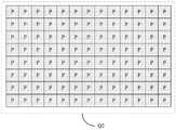
图1示意出一种显示基板的结构示意图;该显示基板包括基底10,基底10划分为显示区Q1、过渡区Q2、安装区Q3;其中,过渡区Q2环绕安装区Q3,显示区Q1环绕过渡区Q2。在显示区Q1、过渡区Q2、安装区Q3均包括呈阵列排布的子像素区;为了描述方便,图1中以显示区Q1、过渡区Q2、安装区Q3的子像素区尺寸排布方式均相同,也即基底10上的各个子像素区呈阵列排布为例。将子像素区分为多类,分别为第一类子像素区P、第二类子像素区D、第三类子像素区A、第四类子像素区K;其中,第一类子像素区P用于设置像素电路,像素电路包括驱动子电路20和发光器件OLED;第二类子像素区D用于设置驱动子电路20;第三类子像素区A用于设置发光器件OLED;第四类子像素区K为空缺像素区,也就是说第四类子像素区K中不设置任何像素元件(例如:薄膜晶体管、发光器件OLED等)。1 shows a schematic structural diagram of a display substrate; the display substrate includes a
具体的,像素电路中的驱动子电路20至少包括开关晶体管和驱动晶体管,当然还可以包括阈值补偿晶体管、存储电容等结构,如图2所示,给出一种示例性的像素电路。该像素电路包括驱动子电路20和发光器件OLED;其中,驱动子电路20具体包括:第一复位晶体管T1、阈值补偿晶体管T2、驱动晶体管T3、开关晶体管T4、第一发光控制晶体管T5、第二发光控制晶体管T6、第二复位晶体管T7、第一存储电容C1;其中,第一晶体管T1的第一极连接初始电压信号端Vint,第一复位晶体管T1的第二极连接第一存储电容C1的第二端、阈值补偿晶体管T2的第一极和驱动晶体管T3的控制极,第一复位晶体管T1的控制极连接复位信号端Reset;阈值补偿晶体管T2的第二极连接驱动晶体管T3的第二极和第二发光控制晶体管T6的第一极,阈值补偿晶体管T2的控制极连接栅线Gate;驱动晶体管T3的第一极连接第一电源线VDD;开关晶体管T4的第一极连接数据线Data,开关晶体管T4的第二极连接第一发光控制晶体管T5的第二极、第二复位晶体管T7的第二极和第一存储电容C1的第一极;开关晶体管T4的控制极连接栅线Gate;第一发光控制晶体管T5的第一极连接基准电压信号端Vref,第一发光控制晶体管T5的控制极连接发光控制线EM;第二发光控制晶体管T6的第二极连接发光器件OLED的第一电极,第二发光控制晶体管T6的控制极连接发光控制线EM;第二复位晶体管T7的第一极连接基准电压信号端Vref,第二复位晶体管T7的控制极连接复位信号端Reset,发光器件OLED的第二电极连接第二电源线VSS。Specifically, the
在此需要说明的是,驱动子电路20与栅线Gate连接是指驱动子电路20中的开关晶体管的控制极连接栅线Gate;驱动子电路20与数据线Data连接是指开关晶体管的第一极连接数据线Data;驱动子电路20与发光器件OLED连接是指驱动子电路20的驱动晶体管的第二极与发光器件OLED的第一极连接。It should be noted here that the connection between the driving
其中,上述的所采用的晶体管可以为薄膜晶体管或场效应管或其他特性的相同器件,由于采用的晶体管的源极和漏极是对称的,所以其源极、漏极是没有区别的。在本发明实施例中,为区分晶体管的源极称之为第一极,漏极称之为第二极,栅极称为控制极。此外按照晶体管的特性区分可以将晶体管分为N型和P型,当采用P型晶体管时,第一极为P型晶体管的源极,第二极为P型晶体管的漏极,栅极输入低电平时,源漏极导通;当采用N型晶体管时,第一极为N型晶体管的源极,第二极为N型晶体管的漏极,栅极输入高电平时,源漏极导通。其中,上述的像素电路中的晶体管均是以N型晶体管为例进行说明的,可以想到的是采用P型晶体管实现是本领域技术人员可以在没有付出创造性劳动前提下轻易想到的,因此也是在本公开实施例的保护范围内的。The above-mentioned transistors used may be thin film transistors or field effect transistors or other devices with the same characteristics. Since the source and drain electrodes of the used transistors are symmetrical, there is no difference between the source and drain electrodes. In the embodiments of the present invention, to distinguish the source of the transistor is called the first electrode, the drain is called the second electrode, and the gate is called the control electrode. In addition, according to the characteristics of transistors, transistors can be divided into N-type and P-type. When a P-type transistor is used, the first pole is the source of the P-type transistor, the second pole is the drain of the P-type transistor, and when the gate is input low level , the source and drain are turned on; when an N-type transistor is used, the first pole is the source of the N-type transistor, the second pole is the drain of the N-type transistor, and when the gate is input with a high level, the source and drain are turned on. Among them, the transistors in the above-mentioned pixel circuits are all described by taking N-type transistors as an example. It is conceivable that the use of P-type transistors can be easily thought of by those skilled in the art without creative work. within the scope of protection of the embodiments of the present disclosure.
其中,图1所示的显示基板特别适用于屏下安装摄像头的显示面板中。安装区Q3则对应安装摄像头元件,显示区Q1用于画面的显示。由于过渡区Q2和安装区Q3无需显示画面,故二者像素分辨率可以小于显示区Q1的像素分辨率。同时,由于摄像头安装在屏下,故为避免安装区Q3的像素元件(例如:薄膜晶体管、发光器件OLED等元件)遮挡摄像头,故仅在安装区Q3设置透明发光器件OLED。应当理解的是,在下述描述中安装区Q3中的发光器件OLED均是指透明发光器件OLED。Among them, the display substrate shown in FIG. 1 is particularly suitable for a display panel with a camera installed under the screen. The installation area Q3 corresponds to the installation of the camera components, and the display area Q1 is used for the display of the screen. Since the transition area Q2 and the installation area Q3 do not need to display images, the pixel resolution of the two may be smaller than that of the display area Q1. At the same time, since the camera is installed under the screen, in order to avoid the pixel elements (such as thin film transistors, light-emitting device OLEDs, etc.) in the mounting area Q3 from blocking the camera, only the transparent light-emitting device OLED is arranged in the mounting area Q3. It should be understood that, in the following description, the light emitting device OLED in the mounting area Q3 refers to the transparent light emitting device OLED.
图3给出一种显示基板的显示区Q1的像素排布示意图;如图3所示,显示区Q1中的子像素区仅包括第一类子像素区P;也即在显示区Q1的每个子像素区中均设置有像素电路。对于位于显示区Q1中的各个子像素区中的像素电路而言,其中,位于同一行的像素电路通过同一条栅线Gate进行控制,位于同一列像素电路由同一条数据线Data进行数据写入。FIG. 3 shows a schematic diagram of the pixel arrangement of the display area Q1 of a display substrate; as shown in FIG. 3 , the sub-pixel area in the display area Q1 only includes the first type of sub-pixel area P; Each of the sub-pixel regions is provided with pixel circuits. For the pixel circuits located in each sub-pixel area in the display area Q1, the pixel circuits located in the same row are controlled by the same gate line Gate, and the pixel circuits located in the same column are data written by the same data line Data .
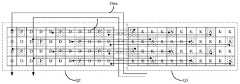
图4给出一种显示基板的过渡区Q2和安装区Q3的像素排布示意图。如图4所示,过渡区Q2中的子像素区包括第一类子像素区P和第二类子像素区D,也即在部分子像素区中设置像素电路,部分子像素区中仅设置驱动子电路20。安装区Q3中子像素区包括第三类子像素区A和第四类子像素区K,也即在部分子像素区中设置发光器件OLED,剩余的子像素则为空缺像素区,不设置任何像素元件。其中,安装区Q3的第三类子像素区A中设置发光器件OLED通过过渡区Q2的第二类子像素区D中的驱动子电路20进行驱动。具体的,位于安装区Q3的第三类子像素区A中的发光器件OLED通过信号连接线1与位于过渡区Q2的第二类子像素区D中的驱动子电路20连接。位于安装区Q3的各个发光器件OLED的数据信号,是通过数据线Data从安装区Q3和过渡区Q2之间绕线的方式与过渡区Q2的第二类子像素区D中的驱动子电路20连接。其中,为了便于发光器件OLED的驱动,安装区Q3的第三类子像素区A中的发光器件OLED通过信号连接和与之位于同一行的、且位于过渡区Q2的第二类子像素区D中的驱动子电路20连接。应当理解的是,每一发光器件OLED通过与之对应的信号连接线1,连接一个驱动子电路20,不同的发光器件OLED连接不同的驱动子电路20。FIG. 4 shows a schematic diagram of the arrangement of pixels in the transition area Q2 and the mounting area Q3 of a display substrate. As shown in FIG. 4 , the sub-pixel area in the transition area Q2 includes a first-type sub-pixel area P and a second-type sub-pixel area D, that is, pixel circuits are provided in some sub-pixel areas, and only some sub-pixel areas are provided
发明人发现,安装区Q3的每一发光器件OLED需要通过信号连接线1,与过渡区Q2中与其同行的第二类子像素区D中的驱动子电路20连接,这样导致,摄像头的尺寸较大或者设置多个摄像头时,而过渡区Q2的面积一定的情况下,过渡区可以布置的信号连接线1的数量将会受限,从而导致可以控制的发光器件OLED的数量受限,进而导致安装区Q3的面积较小,进而导致设置大尺寸的摄像头或者设置多个摄像头受限。The inventor found that each light-emitting device OLED in the mounting area Q3 needs to be connected to the driving
针对上述问题,本公开实施例提供下述技术方案。In view of the above problems, the embodiments of the present disclosure provide the following technical solutions.
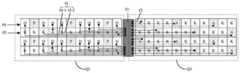
第一方面,如图1、4、5-8所示,本公开实施例提供一种显示基板,显示基板包括基底10,基底10划分为显示区Q1、过渡区Q2、安装区Q3;其中,过渡区Q2环绕安装区Q3,显示区Q1环绕过渡区Q2。在显示区Q1、过渡区Q2、安装区Q3均包括呈阵列排布的子像素区。其中,位于过渡区Q2中的子像素区至少包括第一类子像素区P和第二类子像素区D;安装区Q3中的子像素区至少包括第三类子像素区A;在第一类子像素区P中设置有位于基底10上的像素电路;像素电路包括驱动子电路20和发光器件OLED;在第二类子像素区D中设置有位于基底10上的驱动子电路20;在第三类子像素区A中设置有位于基底10上发光器件OLED;其中,位于安装区Q3的第三类子像素区A中的发光器件OLED,通过信号连接线1与位于过渡区Q2的第二类子像素区D中的驱动子电路20连接;且不同的发光器件OLED所连接的信号连接线1和驱动子电路20均不同;至少部分信号连接线1在基底10上的正投影存在重叠。In the first aspect, as shown in FIGS. 1, 4, and 5-8, an embodiment of the present disclosure provides a display substrate. The display substrate includes a
在此需要说明的是,信号连接线1与安装区Q3的发光器件OLED一一对应设置,也即一条信号连接线1仅为一个发光器件OLED提供驱动电流,这样一来,各信号连接线1不能发生短接,故应当理解的是,虽然在本公开实施例中至少部分信号连接线1在基底10上存在交叠,但任意两条正投影存在交叠的信号连接线1至少二者交叠的位置设置在不同层中,且这两层之间设置有层间绝缘层,将二者分隔开,以避免信号连接线1短接。It should be noted here that the signal connection line 1 is set in a one-to-one correspondence with the light-emitting device OLED in the mounting area Q3, that is, a signal connection line 1 only provides a driving current for one light-emitting device OLED. In this way, each signal connection line 1 No short circuit can occur, so it should be understood that although at least some of the signal connection lines 1 overlap on the
另外,显示区Q1、过渡区Q2、安装区Q3的形状可以为圆形、方形、多边形等各种形状,且三者的形状可以相同,也可以不同,在本公开实施例中并不对显示区Q1、过渡区Q2、安装区Q3的形状进行限制。对于安装区Q3中可以安装摄像头,还可以安装传感器、HOME键、听筒或扬声器等器件,对此在本公开实施例中不进行限定,在下述描述中是以安装区Q3安装摄像头为例进行说明的。In addition, the shapes of the display area Q1, the transition area Q2, and the installation area Q3 may be various shapes such as circle, square, and polygon, and the shapes of the three may be the same or different. The shapes of Q1, transition area Q2, and mounting area Q3 are limited. A camera can be installed in the installation area Q3, and devices such as sensors, HOME keys, earpieces, or speakers can also be installed, which are not limited in the embodiments of the present disclosure. In the following description, the installation area Q3 is used as an example for installation of a camera. of.
由于在本公开实施例的显示基板中,至少部分用于连接过渡区Q2的驱动子电路20和安装区Q3的发光器件OLED的信号连接线1在基底10上的正投影存在交叠,故可以在过渡区Q2的空间一定的情况下,此时可以在过渡区Q2设置更多条信号连接线1,以能够满足较大尺寸的摄像头或者多个摄像头设置对安装区Q3面积大小的需求。In the display substrate of the embodiment of the present disclosure, at least part of the orthographic projection of the signal connection line 1 for connecting the driving
在一些实施例中,为了使得安装区Q3和过渡区Q2显示均匀,在安装区Q3和过渡区Q2中的发光器件的排布方式相同。也即在过渡区Q2中每间隔几个子像素区设置一个发光器件OLED(该发光器件OLED可以是第一类子像素区P中的像素电路的发光器件OLED,也可以是第三类子像素区A中的发光器件OLED),同样在安装区Q3间隔相同数量的子像素区设置一个发光器件OLED。在本公开实施例中均以在安装区Q3和过渡区Q2中的发光器件的排布方式相同为例进行说明。In some embodiments, in order to make the mounting area Q3 and the transition area Q2 display uniform, the light emitting devices in the mounting area Q3 and the transition area Q2 are arranged in the same manner. That is, a light-emitting device OLED is arranged every several sub-pixel regions in the transition region Q2 (the light-emitting device OLED can be the light-emitting device OLED of the pixel circuit in the first type of sub-pixel region P, or it can be a third-type sub-pixel region. The light-emitting device OLED in A), a light-emitting device OLED is also arranged in the mounting region Q3 with the same number of sub-pixel regions. In the embodiments of the present disclosure, the arrangement of the light emitting devices in the mounting region Q3 and the transition region Q2 is the same as an example for description.
在一些实施例中,如图5所示,每条信号连接线1均包括设置在过渡区Q2的第一子连接线11和设置在安装区Q3的第二子连接线12。由于安装区Q3需要设置摄像头,故安装区Q3至少设置摄像头的位置透过区,因此,第二子连接线12需要选用透明导电材料(例如:氧化铟锡;ITO)。为了使得在过渡区Q2面积有限的情况下设置更多信号连接线1,以为安装区Q3更多的发光器件OLED提供驱动电流,在本公开实施例中至少部分第一子连接线11设置在不同层中,且至少部分设于不同层中第一子连接线11在基底10上的正投影存在交叠。In some embodiments, as shown in FIG. 5 , each signal connection line 1 includes a first
当然,在本公开实施例中信号连接线1可以采用透明导电材料,此时只需将部分信号连接线1设置在不同层,且设置在不同层的信号连接线1在基底10上的投影存在交叠,这样一来,也可以节约过渡区Q2的布线空间,且不会降低安装区Q1的透过率。Of course, in the embodiment of the present disclosure, the signal connection lines 1 can be made of transparent conductive materials. In this case, only part of the signal connection lines 1 need to be arranged in different layers, and the projections of the signal connection lines 1 arranged in different layers on the
在一些实施例中,如图5所示,当每条信号连接线1的第一子连接线11和第二子连接线12设置在不同层时,在第一子连接线11所在层和第二子连接线12所在层之间设置有层间绝缘层,每条信号连接线1的第一子连接线11和第二子连接线12则可以通过贯穿层绝缘层的过孔连接。在此需要说明的是,图5中13的位置代表第一子连接线11与第二子连接线12跨层连接的位置。In some embodiments, as shown in FIG. 5 , when the first
在一些实施例中,驱动子电路20包括薄膜晶体管,例如包括如图2中所示的7个晶体管。具体的,以图6所示的驱动晶体管M3和发光器件OLED的连接示意图为例。其中,驱动晶体管包括位于基底10上的半导体有源层31、设置半导体有源层31之上的栅极绝缘层101,设置在栅极绝缘层101之上的栅极32,设置在栅极32之上的层间绝缘层102,设置在层间绝缘层102之上的源极33和漏极34。在驱动晶体管M3的源极33和漏极34的所在层至上设置有平坦化层103,发光器件OLED设置在平坦化层103之上。In some embodiments, the driver sub-circuit 20 includes thin film transistors, eg, including 7 transistors as shown in FIG. 2 . Specifically, take the connection diagram of the driving transistor M3 and the light emitting device OLED shown in FIG. 6 as an example. The driving transistor includes a semiconductor
在本公开实施例中,如图6所示,各信号连接线1的第一子连接线11中的部分可以与薄膜晶体管的源极和漏极同层设置,且材料相同,另一部分可以与薄膜晶体管的栅极同层设置,且材料相同。如此设置,可以通过一次构图工艺在形成薄膜晶体管的源极和漏极的同时形成一部分第一子连接线11-2,通过一次构图工艺形成薄膜晶体管的栅极的同时形成另一部第一子连接线11-1,因此即使在本公开实施例中信号连接由两层结构形成组成,但并不会增加显示基板的厚度,而且也不会增加工艺成本。同时,由于薄膜晶体管的源极、漏极、栅极均采用金属材料,而金属材料相较ITO而言电阻较小,故采用源极、漏极或者栅极的材料作为第一子连接线11的材料,所形成信号连接线1的电阻降低,有助于驱动电流的传输。In the embodiment of the present disclosure, as shown in FIG. 6 , part of the first
在此需要说明的是,在本公开实施例中是以一部分第一子连接线11与薄膜薄膜晶体管的源极和漏极同层设置,另一部分第一子连接线11与薄膜晶体管的栅极同层设置为例进行说明的。当然,一条第一子连接线11也可以是由与薄膜薄膜晶体管的源极和漏极同层设置第一子结构和与薄膜晶体管的栅极的同层设置的第二子结构连接组成;或者,各个第一子连接线11不与薄膜晶体管的源极、漏极、栅极同层设置也是可行的,只要保证部分第一子连接线11在基底10上的投影存在重叠即可。It should be noted here that, in the embodiment of the present disclosure, a part of the first
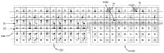
在一些实施例中,过渡区Q2中还包括第四类子像素区K,也即过渡区Q2中包括空缺像素区。将过渡区Q2中具有与安装区Q3的发光器件OLED连接驱动子电路20的一行子像素区记作第一像素行P1;将过渡区Q2中至少具有第四类子像素区K,且不具有第一类子像素区P和第二类子像素区D(也即不设置驱动子电路20)的一行子像素区记作第二像素行P2,。在任意两相邻第一像素行P1之间设置至少一行第二像素行P2,信号连接线1经由第二像素行P2将第一像素行P1中的驱动子电路20与安装区Q3的发光器件OLED连接。In some embodiments, the transition area Q2 further includes a fourth type of sub-pixel area K, that is, the transition area Q2 includes a vacant pixel area. A row of sub-pixel regions in the transition region Q2 having the driving
由于在过渡区Q2设置第一像素行P1,且在第一像素行P1中具有第四类子像素区K,且不设置驱动子电路20,这样一来,为信号连接线1提供了一定的布线空间,因此可以在过渡区Q2设置较多的信号连接线1,为安装区Q3更多的发光器件OLED提供驱动电流,与此同时,安装区Q3的面积可以相应的扩大,有助于大尺寸的摄像头及多个摄像头的设置。Since the first pixel row P1 is arranged in the transition region Q2, and the fourth type of sub-pixel region K is provided in the first pixel row P1, and the driving
在一些实施例中,第二像素行P2中还具有第三类子像素区A,且该第三类子像素区A中发光器件OLED与第一像素行P1的第二类子像素区D中的驱动子电路20连接。具体的,第二像素行P2的第三类子像素区A中的发光器件OLED所连接的第一像素行P1中的第一像素行P1的第二类子像素区D中的驱动子电路20位于同一列,且设置在相邻的子像素区中,如此设置方便第三类子像素区A中发光器件OLED与第一像素行P1的第二类子像素区D中的驱动子电路20连接。In some embodiments, the second pixel row P2 further has a third type of sub-pixel area A, and the light-emitting device OLED in the third type of sub-pixel area A and the second type of sub-pixel area D in the first pixel row P1 The driver sub-circuit 20 is connected. Specifically, the driving
在一些实施例中,第一像素行P1中还具有设置有像素电路的第一类子像素区P;第一像素行P1的像素电路的发光器件OLED和安装区Q3中的与之同行的发光器件OLED按照一定规律进行排布,也就说贯穿过渡区Q2和安装区Q3的每一行子像素区中的发光器件OLED按照预设规律进行排布。例如:对于每一行子像素区,每间隔三个子像素区设置的子像素区中设置有一个发光器件OLED(这个发光器件OLED可以是像素电路中的发光器件OLED,也可以是单独的发光器件OLED),为了过渡区Q2和安装区Q3显示均匀任意相邻行子像素中发光器件OLED交错设置,且在行方向间隔一个子像素区。当然,以上只是给出一个示例性的发光器件OLED的排布方式,还根据安装区Q3和过渡区Q2的尺寸对发光器件OLED设置位置进行调整。In some embodiments, the first pixel row P1 also has a first type of sub-pixel region P provided with pixel circuits; the light emitting device OLED of the pixel circuit of the first pixel row P1 and the mounting region Q3 in the same row emit light. The device OLEDs are arranged according to a certain rule, that is to say, the light-emitting devices OLEDs in each row of sub-pixel regions running through the transition region Q2 and the mounting region Q3 are arranged according to a preset rule. For example: for each row of sub-pixel regions, there is one light-emitting device OLED in the sub-pixel regions arranged every three sub-pixel regions (the light-emitting device OLED can be the light-emitting device OLED in the pixel circuit, or it can be a separate light-emitting device OLED ), in order for the transition area Q2 and the mounting area Q3 to display uniformly, the light-emitting devices OLEDs in any adjacent row of sub-pixels are arranged staggered, and one sub-pixel area is spaced apart in the row direction. Of course, the above is only an exemplary arrangement of the light-emitting device OLED, and the arrangement position of the light-emitting device OLED is also adjusted according to the size of the mounting area Q3 and the transition area Q2.
在一些实施例中,将安装区Q3中的发光器件OLED划分为多组,每组包括相邻设置的N行发光器件OLED,N为整数且N≥2;其中,安装区Q3中位于同一组的发光器件OLED所连接的驱动子电路20位于同一第一像素行P1中;任意两相邻的第一像素行P1之间间隔N-1行第二像素行P2。In some embodiments, the light-emitting devices OLED in the mounting area Q3 are divided into multiple groups, each group includes N rows of light-emitting devices OLEDs arranged adjacently, N is an integer and N≥2; wherein, the mounting area Q3 is located in the same group The driving
在一个示例中,如图7所示,N=2,也即安装区Q3中的每组发光器件OLED位于两行子像素区中;任意两相邻的第一像素行P1之间间隔一行第二像素行P2,每个第一像素行P1两相邻的第一类子像素区P之间设置三个第二类子像素区D,也就是说,在第一像素行P1的两个像素电路之间设置三个驱动子电路20,此时这三个驱动子电路20中的两个与安装区Q3的两个位于不同行的发光器件OLED连接。In an example, as shown in FIG. 7 , N=2, that is, each group of light-emitting devices OLED in the mounting area Q3 is located in two rows of sub-pixel areas; there is a row of first pixel rows between any two adjacent first pixel rows P1. Two pixel rows P2, three second-type sub-pixel areas D are set between two adjacent first-type sub-pixel areas P in each first pixel row P1, that is, two pixels in the first pixel row P1
具体的,以过渡区Q2中的第一个第一像素行P1与安装区Q3的第一组发光器件OLED(第一行和第二行的发光器件OLED)连接为例,对于位于第一像素行P1中两个第一类子像素区P之间三个第二类子像素区D中的第一个和第三个第三类子像素区A中的驱动子电路20,一者与安装区Q3的第一行的一个发光器件OLED,另一者则与安装区Q3的第二行的一个发光器件OLED连接。Specifically, taking the connection between the first first pixel row P1 in the transition region Q2 and the first group of light-emitting devices OLED (the light-emitting device OLEDs in the first row and the second row) in the mounting region Q3 as an example, for the first pixel row P1 in the first pixel The driving
如图7所示,第一像素行P1相邻的第二像素行P2中,与任意两相邻的第一类子像素区P之间设置的第二个第二类子像素区D位于同一列的子像素区为第三类子像素区A,其中设置有发光器件OLED,第二像素行P2的其余子像素区为第四类子像素区K。对于位于第一像素行P1中两个第一类子像素区P之间三个第二类子像素区D中的第二个第三类子像素区A中的驱动子电路20和与之相邻的一行第二像素行P2中的发光器件OLED连接。As shown in FIG. 7 , in the second pixel row P2 adjacent to the first pixel row P1, the second second type sub-pixel region D disposed between any two adjacent first-type sub-pixel regions P is located in the same The sub-pixel regions of the column are the third-type sub-pixel regions A, in which the light-emitting devices OLED are disposed, and the remaining sub-pixel regions of the second pixel row P2 are the fourth-type sub-pixel regions K. For the driving
在此需要说明的是,以上是以安装区Q3的二行发光器件OLED为一组,且一组发光器件OLED由一行第一像素行P1中驱动子电路20进行控制。在实际应用中,可以根据摄像头的尺寸数量确定安装区Q3的尺寸,相应的在每行第一像素行P1中设置相应数量的驱动子电路20,以驱动安装区Q3中的发光器件OLED,再根据信号连接线1所需的布线空间决定每行第一像素行P1中驱动子电路20所驱动的安装区Q3中的发光器件OLED的行数。It should be noted here that the above two rows of light-emitting devices OLED in the mounting area Q3 are used as a group, and a group of light-emitting devices OLED is controlled by the driving
在一些实施例中,将安装区Q3中的发光器件OLED划分为多组,每组包括相邻设置的每M行发光器件OLED,M≥4;且位于同一组的发光器件OLED所连接的驱动子电路20位于两行第一像素行P1中;用于连接所述安装区Q3的同一组发光器件OLED的两行第一像素行P1之间间隔M-1行第二像素行P2。In some embodiments, the light-emitting devices OLEDs in the mounting area Q3 are divided into multiple groups, each group includes adjacently arranged light-emitting devices OLEDs in every M rows, M≥4; and the drivers connected to the light-emitting devices OLEDs located in the same group The sub-circuits 20 are located in two rows of first pixel rows P1; the two rows of first pixel rows P1 for connecting the same group of light emitting devices OLED in the mounting area Q3 are separated by M-1 rows of second pixel rows P2.
在一个示例中,如图8所示,M=4,每一所述第一像素行P1的第二类子像素区D中的驱动子电路20连接安装区Q3两行发光器件OLED;且不同的第一像素行P1中第二类子像素区D中的驱动子电路20连接的所述发光器件OLED位于不同行;在第一像素行P1中两相邻的第一类子像素区P中之间设置有三个所述第二类子像素区D,也就是说,在第一像素行P1的两个像素电路之间设置三个驱动子电路20,此时这三个驱动子电路20中的两个与安装区Q3的两个位于不同行的发光器件OLED连接。In an example, as shown in FIG. 8, M=4, the driving
具体的,以过渡区Q2中的第一个和第二个第一像素行P1与安装区Q3的第一组发光器件OLED(第一行、第二行、第三行和第四行的发光器件OLED)连接为例,在第一个和第二个第一像素行P1之间设置两个第二像素行P2,对于位于第一个第一像素行P1中两个第一类子像素区P之间三个第二类子像素区D中的第一个和第三个第三类子像素区A中的驱动子电路20,一者与安装区Q3的第一行的一个发光器件OLED,另一者则与安装区Q3的第二行的一个发光器件OLED连接。对于位于第二个第一像素行P1中两个第一类子像素区P之间三个第二类子像素区D中的第一个和第三个第三类子像素区A中的驱动子电路20,一者与安装区Q3的第三行的一个发光器件OLED,另一者则与安装区Q3的第四行的一个发光器件OLED连接。Specifically, the first and second first pixel rows P1 in the transition area Q2 and the first group of light-emitting devices OLED in the mounting area Q3 (the first row, the second row, the third row and the fourth row emit light The device OLED) is connected as an example, two second pixel rows P2 are set between the first and second first pixel rows P1, for the two first-type sub-pixel regions located in the first first pixel row P1 One of the driving
如图8所示,与第一个第一像素行P1相邻的第一个第二像素行P2中,与任意两相邻的第一类子像素区P之间设置的第二个第二类子像素区D位于同一列的子像素区为第三类子像素区A,其中设置有发光器件OLED,第一个第二像素行P2的其余子像素区为第四类子像素区K。对于位于第一像素行P1中两个第一类子像素区P之间三个第二类子像素区D中的第二个第三类子像素区A中的驱动子电路20和与第一个第二像素行P2中的发光器件OLED连接。与第二个第一像素行P1相邻的第二个第二像素行P2中,与第二个第一像素行P1中两相邻的第一类子像素区P之间设置的第二个第二类子像素区D位于同一列的子像素区为第三类子像素区A,其中设置有发光器件OLED,第二个第二像素行P2的其余子像素区为第四类子像素区K。对于位于第一像素行P1中两个第一类子像素区P之间三个第二类子像素区D中的第二个第三类子像素区A中的驱动子电路20和与之相邻的一行第二像素行P2中的发光器件OLED连接。As shown in FIG. 8 , in the first second pixel row P2 adjacent to the first first pixel row P1, the second second pixel area P is arranged between any two adjacent first type sub-pixel regions P. The sub-pixel regions D located in the same column are the third-type sub-pixel regions A, in which the light-emitting devices OLED are disposed, and the remaining sub-pixel regions of the first second pixel row P2 are the fourth-type sub-pixel regions K. For the driving
在此需要说明的是,以上是以安装区Q3的四行发光器件OLED为一组,且一组发光器件OLED由两行第一像素行P1中驱动子电路20进行控制。在实际应用中,可以根据摄像头的尺寸数量确定安装区Q3的尺寸,相应的在每行第一像素行P1中设置相应数量的驱动子电路20,以驱动安装区Q3中的发光器件OLED,再根据信号连接线1所需的布线空间决定每行第一像素行P1中驱动子电路20所驱动的安装区Q3中的发光器件OLED的行数。It should be noted here that the above is a group of four rows of light-emitting devices OLED in the mounting area Q3, and a group of light-emitting devices OLED is controlled by the driving
在一些实施例中,显示基板上还设置有多条栅线Gate,位于同一行的发光器件OLED所连接驱动子电路20连接同一条栅线Gate。由于安装区Q3中需设置摄像头,栅线Gate的材料为遮光的材料,故在栅线Gate需要在安装区Q3的周边区域进行绕线,同时,在安装区Q3也不能够设置驱动子电路20,以避免栅线Gate贯穿安装区Q3,以及驱动子电路20的设置遮挡摄像头。In some embodiments, a plurality of gate lines Gate are further disposed on the display substrate, and the driving
可以理解的是,显示区Q1中的各个子像素中均设置有像素电路,也即显示区Q1中的各个子像素区均为第一类子像素区P,显示区Q1中的每一行像素电路中的驱动子电路20连接同一条栅线Gate,而对于每个驱动子电路20中均设置有存储电容(也即图2中存储电容C1)。It can be understood that each sub-pixel in the display area Q1 is provided with a pixel circuit, that is, each sub-pixel area in the display area Q1 is the first type of sub-pixel area P, and each row of pixel circuits in the display area Q1
由于第一像素行P1的第二类子像素区D中的驱动子电路20分别于与安装区Q3中的发光器件OLED连接以及第二像素行P2中的发光器件OLED连接,故导致第一像素行P1中的驱动子电路20所连接栅线Gate上的存储电容数量少于显示区Q1中每一条栅线Gate上所连接的存储电容的数量,因此,如图7和8所示,在本公开实施例的过渡区Q2中还设置有第五类子像素区,在第五类子像素区中形成有补偿电容30,与安装区Q3的发光器件OLED连接的驱动子电路20所连接的栅线Gate与补偿电容30的第一极板连接,且连接安装区Q3中不同行的发光器件OLED的驱动子电路20所连接的栅线Gate所连接补偿电容30不同。Since the driving
在一些实施例中,与第五类子像素区J位于同一行的各个子像素区中的驱动子电路20所连接的栅线Gate同样连接补偿电容30,且不同的栅线Gate连接不同的补偿电容30。In some embodiments, the gate lines connected to the driving
具体的,在相关技术中,在安装区Q3上方的过渡区Q2中各行子像素区中均为第一类子像素区P和第二类子像素区D;第一类子像素区P中设置有像素电路;第二类子像素区D中设置有驱动子电路20。如图7和8所示,在本公开实施例中,可以将安装区Q3上方的部分第二类子像素区D替换为第五类子像素区J,在第五类子像素区J中形成补偿电容30,补偿电容30的第一极板连接安装区Q3中的发光器件OLED连接的驱动子电路20所连接的栅线Gate。与此同时,由于过渡区Q2中部分子像素区为第五类子像素区J,因此导致设置第五类子像素区J的一行子像素区所对应的栅线Gate连接的存储电容的数量少于显示区Q1中栅线Gate所连接的存储电容的数量,故在具有第五类子像素区J一行子像素区中设置多个第五类子像素区J,以使具有第五类子像素区J一行子像素区所对应的栅线Gate可以与该行的第五类子像素区J中的补偿电容30连接,以避免显示画面较暗的问题。Specifically, in the related art, each row of sub-pixel regions in the transition region Q2 above the mounting region Q3 is a first-type sub-pixel region P and a second-type sub-pixel region D; There are pixel circuits; the second type of sub-pixel area D is provided with a driving
在一些实施例中,补偿电容30的第一极板与栅线Gate连接,并与栅线Gate同层设置且材料相同,补偿电容30的第二极板与第一电源线VDD连接,并与第一电源线VDD同层设置且材料相同。这样一来,并不会增加工艺步骤,也不会增加显示基板的厚度。In some embodiments, the first plate of the
第二方面,本公开实施例还提供一种显示面板,该显示面板包括上述的显示基板。该显示面板例如可为手机、平板电脑、电子手表、运动手环、笔记本电脑等具有显示面板的电子设备。该显示装置具有的技术效果可参考上述对显示面板的技术效果的论述,在此不再赘述。In a second aspect, an embodiment of the present disclosure further provides a display panel including the above-mentioned display substrate. The display panel can be, for example, an electronic device having a display panel, such as a mobile phone, a tablet computer, an electronic watch, a sports bracelet, and a notebook computer. For the technical effect of the display device, reference may be made to the above discussion on the technical effect of the display panel, which will not be repeated here.
可以理解的是,以上实施方式仅仅是为了说明本发明的原理而采用的示例性实施方式,然而本发明并不局限于此。对于本领域内的普通技术人员而言,在不脱离本发明的精神和实质的情况下,可以做出各种变型和改进,这些变型和改进也视为本发明的保护范围。It can be understood that the above embodiments are only exemplary embodiments adopted to illustrate the principle of the present invention, but the present invention is not limited thereto. For those skilled in the art, without departing from the spirit and essence of the present invention, various modifications and improvements can be made, and these modifications and improvements are also regarded as the protection scope of the present invention.
Claims (17)
Translated fromChinesePriority Applications (3)
| Application Number | Priority Date | Filing Date | Title |
|---|---|---|---|
| CN202010352241.8ACN111446282B (en) | 2020-04-28 | 2020-04-28 | Display substrate and display device |
| US17/637,897US12232361B2 (en) | 2020-04-28 | 2021-03-12 | Display substrate having sub-pixel areas and display apparatus including the same |
| PCT/CN2021/080353WO2021218437A1 (en) | 2020-04-28 | 2021-03-12 | Display substrate and display device |
Applications Claiming Priority (1)
| Application Number | Priority Date | Filing Date | Title |
|---|---|---|---|
| CN202010352241.8ACN111446282B (en) | 2020-04-28 | 2020-04-28 | Display substrate and display device |
Publications (2)
| Publication Number | Publication Date |
|---|---|
| CN111446282A CN111446282A (en) | 2020-07-24 |
| CN111446282Btrue CN111446282B (en) | 2022-04-22 |
Family
ID=71651959
Family Applications (1)
| Application Number | Title | Priority Date | Filing Date |
|---|---|---|---|
| CN202010352241.8AActiveCN111446282B (en) | 2020-04-28 | 2020-04-28 | Display substrate and display device |
Country Status (3)
| Country | Link |
|---|---|
| US (1) | US12232361B2 (en) |
| CN (1) | CN111446282B (en) |
| WO (1) | WO2021218437A1 (en) |
Families Citing this family (15)
| Publication number | Priority date | Publication date | Assignee | Title |
|---|---|---|---|---|
| CN111446282B (en) | 2020-04-28 | 2022-04-22 | 京东方科技集团股份有限公司 | Display substrate and display device |
| CN112038380B (en)* | 2020-09-08 | 2023-04-07 | 京东方科技集团股份有限公司 | Display substrate and display device |
| CN114556582A (en)* | 2020-09-24 | 2022-05-27 | 京东方科技集团股份有限公司 | Display panel, display device and manufacturing method |
| EP4203046A4 (en) | 2020-09-30 | 2023-11-01 | BOE Technology Group Co., Ltd. | DISPLAY PANEL AND DISPLAY DEVICE |
| CN115104186B (en)* | 2020-11-27 | 2023-08-22 | 京东方科技集团股份有限公司 | Display substrate, display panel, display device |
| CN114566522B (en)* | 2020-11-27 | 2025-08-08 | 京东方科技集团股份有限公司 | Display substrate and display device |
| WO2022134097A1 (en)* | 2020-12-25 | 2022-06-30 | 京东方科技集团股份有限公司 | Display panel and display device |
| EP4141948A4 (en) | 2021-02-19 | 2023-10-04 | BOE Technology Group Co., Ltd. | DISPLAY BOARD AND DISPLAY DEVICE |
| CN113161402A (en)* | 2021-04-23 | 2021-07-23 | 京东方科技集团股份有限公司 | Display substrate and display device |
| CN113539161B (en)* | 2021-06-30 | 2022-05-31 | 武汉天马微电子有限公司 | Display panel and display device |
| KR20230010083A (en)* | 2021-07-08 | 2023-01-18 | 삼성디스플레이 주식회사 | Display device |
| CN117016053A (en)* | 2022-03-01 | 2023-11-07 | 京东方科技集团股份有限公司 | Display panel, preparation method thereof and display device |
| KR20230139709A (en)* | 2022-03-28 | 2023-10-05 | 엘지디스플레이 주식회사 | Display panel and display device |
| CN115132128B (en)* | 2022-06-30 | 2025-03-18 | 湖北长江新型显示产业创新中心有限公司 | Display panel and display device |
| CN115472664A (en)* | 2022-10-14 | 2022-12-13 | 昆山国显光电有限公司 | Display panel and display device |
Citations (6)
| Publication number | Priority date | Publication date | Assignee | Title |
|---|---|---|---|---|
| CN106991969A (en)* | 2017-06-09 | 2017-07-28 | 京东方科技集团股份有限公司 | Display panel, the compensation circuit of pixel and compensation method |
| CN110047901A (en)* | 2019-04-28 | 2019-07-23 | 厦门天马微电子有限公司 | A kind of display panel and electronic equipment |
| CN110265455A (en)* | 2019-06-25 | 2019-09-20 | 武汉华星光电半导体显示技术有限公司 | A kind of display panel and display device |
| CN110278300A (en)* | 2018-08-10 | 2019-09-24 | 友达光电股份有限公司 | display device |
| CN110289299A (en)* | 2019-06-28 | 2019-09-27 | 武汉天马微电子有限公司 | Display panel and display device |
| WO2019199139A1 (en)* | 2018-04-13 | 2019-10-17 | 삼성전자 주식회사 | Display including plurality of wirings bypassing hole area encompassed by display area, and electronic device including same |
Family Cites Families (2)
| Publication number | Priority date | Publication date | Assignee | Title |
|---|---|---|---|---|
| CN115148780B (en)* | 2019-08-27 | 2025-07-15 | 武汉天马微电子有限公司 | Display panel and display device |
| CN111446282B (en) | 2020-04-28 | 2022-04-22 | 京东方科技集团股份有限公司 | Display substrate and display device |
- 2020
- 2020-04-28CNCN202010352241.8Apatent/CN111446282B/enactiveActive
- 2021
- 2021-03-12USUS17/637,897patent/US12232361B2/enactiveActive
- 2021-03-12WOPCT/CN2021/080353patent/WO2021218437A1/ennot_activeCeased
Patent Citations (6)
| Publication number | Priority date | Publication date | Assignee | Title |
|---|---|---|---|---|
| CN106991969A (en)* | 2017-06-09 | 2017-07-28 | 京东方科技集团股份有限公司 | Display panel, the compensation circuit of pixel and compensation method |
| WO2019199139A1 (en)* | 2018-04-13 | 2019-10-17 | 삼성전자 주식회사 | Display including plurality of wirings bypassing hole area encompassed by display area, and electronic device including same |
| CN110278300A (en)* | 2018-08-10 | 2019-09-24 | 友达光电股份有限公司 | display device |
| CN110047901A (en)* | 2019-04-28 | 2019-07-23 | 厦门天马微电子有限公司 | A kind of display panel and electronic equipment |
| CN110265455A (en)* | 2019-06-25 | 2019-09-20 | 武汉华星光电半导体显示技术有限公司 | A kind of display panel and display device |
| CN110289299A (en)* | 2019-06-28 | 2019-09-27 | 武汉天马微电子有限公司 | Display panel and display device |
Also Published As
| Publication number | Publication date |
|---|---|
| US12232361B2 (en) | 2025-02-18 |
| CN111446282A (en) | 2020-07-24 |
| WO2021218437A1 (en) | 2021-11-04 |
| US20220285470A1 (en) | 2022-09-08 |
Similar Documents
| Publication | Publication Date | Title |
|---|---|---|
| CN111446282B (en) | Display substrate and display device | |
| CN107863374B (en) | OLED display panel and display device | |
| CN113078174B (en) | Array substrate, display panel and display device | |
| US20210081063A1 (en) | Flexible display panel and flexible display device | |
| WO2021027109A1 (en) | Display panel and display apparatus | |
| CN113410257B (en) | Array substrate, display panel and display device | |
| US20220376003A1 (en) | Display panel and display apparatus | |
| CN112186021A (en) | Display panel and display device | |
| CN114080689B (en) | Display substrate and display device | |
| CN113972237A (en) | Display panel and display device | |
| US20230402467A1 (en) | Array substrate, display panel and display apparatus | |
| CN112997241B (en) | Array substrate and display panel | |
| CN113871420A (en) | Display substrate and display device | |
| CN111477672A (en) | Display substrate, preparation method thereof, display panel and display device | |
| CN111682054A (en) | Array substrate, display panel and display device | |
| CN110581144A (en) | Thin film transistor components, array substrates and display panels | |
| CN114639698A (en) | Display panels and display devices | |
| CN112038380B (en) | Display substrate and display device | |
| CN110491905A (en) | The manufacturing method of display panel, display device and display panel | |
| WO2024174120A1 (en) | Display substrate and manufacturing method therefor, and display apparatus | |
| WO2018126785A1 (en) | Charge release circuit, display substrate, display device, and charge release method thereof | |
| CN115666175A (en) | display device | |
| CN113380830A (en) | Array substrate, display panel and display device | |
| CN114649394B (en) | Display panel and display device | |
| CN116312384A (en) | Display panel and display device |
Legal Events
| Date | Code | Title | Description |
|---|---|---|---|
| PB01 | Publication | ||
| PB01 | Publication | ||
| SE01 | Entry into force of request for substantive examination | ||
| SE01 | Entry into force of request for substantive examination | ||
| GR01 | Patent grant | ||
| GR01 | Patent grant |