CN111434603A - Microfluidic actuator - Google Patents
Microfluidic actuatorDownload PDFInfo
- Publication number
- CN111434603A CN111434603ACN201910034831.3ACN201910034831ACN111434603ACN 111434603 ACN111434603 ACN 111434603ACN 201910034831 ACN201910034831 ACN 201910034831ACN 111434603 ACN111434603 ACN 111434603A
- Authority
- CN
- China
- Prior art keywords
- layer
- fluid
- outflow holes
- metal layer
- vibration
- Prior art date
- Legal status (The legal status is an assumption and is not a legal conclusion. Google has not performed a legal analysis and makes no representation as to the accuracy of the status listed.)
- Granted
Links
Images


Classifications
- B—PERFORMING OPERATIONS; TRANSPORTING
- B81—MICROSTRUCTURAL TECHNOLOGY
- B81B—MICROSTRUCTURAL DEVICES OR SYSTEMS, e.g. MICROMECHANICAL DEVICES
- B81B3/00—Devices comprising flexible or deformable elements, e.g. comprising elastic tongues or membranes
- B81B3/0018—Structures acting upon the moving or flexible element for transforming energy into mechanical movement or vice versa, i.e. actuators, sensors, generators
- B81B3/0021—Transducers for transforming electrical into mechanical energy or vice versa
- B—PERFORMING OPERATIONS; TRANSPORTING
- B81—MICROSTRUCTURAL TECHNOLOGY
- B81B—MICROSTRUCTURAL DEVICES OR SYSTEMS, e.g. MICROMECHANICAL DEVICES
- B81B1/00—Devices without movable or flexible elements, e.g. microcapillary devices
- B81B1/002—Holes characterised by their shape, in either longitudinal or sectional plane
- B—PERFORMING OPERATIONS; TRANSPORTING
- B81—MICROSTRUCTURAL TECHNOLOGY
- B81C—PROCESSES OR APPARATUS SPECIALLY ADAPTED FOR THE MANUFACTURE OR TREATMENT OF MICROSTRUCTURAL DEVICES OR SYSTEMS
- B81C1/00—Manufacture or treatment of devices or systems in or on a substrate
- B81C1/00015—Manufacture or treatment of devices or systems in or on a substrate for manufacturing microsystems
- B81C1/00023—Manufacture or treatment of devices or systems in or on a substrate for manufacturing microsystems without movable or flexible elements
- B81C1/00119—Arrangement of basic structures like cavities or channels, e.g. suitable for microfluidic systems
- B—PERFORMING OPERATIONS; TRANSPORTING
- B81—MICROSTRUCTURAL TECHNOLOGY
- B81C—PROCESSES OR APPARATUS SPECIALLY ADAPTED FOR THE MANUFACTURE OR TREATMENT OF MICROSTRUCTURAL DEVICES OR SYSTEMS
- B81C1/00—Manufacture or treatment of devices or systems in or on a substrate
- B81C1/00349—Creating layers of material on a substrate
- B—PERFORMING OPERATIONS; TRANSPORTING
- B81—MICROSTRUCTURAL TECHNOLOGY
- B81C—PROCESSES OR APPARATUS SPECIALLY ADAPTED FOR THE MANUFACTURE OR TREATMENT OF MICROSTRUCTURAL DEVICES OR SYSTEMS
- B81C1/00—Manufacture or treatment of devices or systems in or on a substrate
- B81C1/00436—Shaping materials, i.e. techniques for structuring the substrate or the layers on the substrate
- B81C1/00523—Etching material
- F—MECHANICAL ENGINEERING; LIGHTING; HEATING; WEAPONS; BLASTING
- F04—POSITIVE - DISPLACEMENT MACHINES FOR LIQUIDS; PUMPS FOR LIQUIDS OR ELASTIC FLUIDS
- F04B—POSITIVE-DISPLACEMENT MACHINES FOR LIQUIDS; PUMPS
- F04B43/00—Machines, pumps, or pumping installations having flexible working members
- F04B43/02—Machines, pumps, or pumping installations having flexible working members having plate-like flexible members, e.g. diaphragms
- F04B43/04—Pumps having electric drive
- F04B43/043—Micropumps
- F04B43/046—Micropumps with piezoelectric drive
- B—PERFORMING OPERATIONS; TRANSPORTING
- B81—MICROSTRUCTURAL TECHNOLOGY
- B81B—MICROSTRUCTURAL DEVICES OR SYSTEMS, e.g. MICROMECHANICAL DEVICES
- B81B2201/00—Specific applications of microelectromechanical systems
- B81B2201/03—Microengines and actuators
- B81B2201/036—Micropumps
- B—PERFORMING OPERATIONS; TRANSPORTING
- B81—MICROSTRUCTURAL TECHNOLOGY
- B81B—MICROSTRUCTURAL DEVICES OR SYSTEMS, e.g. MICROMECHANICAL DEVICES
- B81B2201/00—Specific applications of microelectromechanical systems
- B81B2201/03—Microengines and actuators
- B81B2201/037—Microtransmissions
- B—PERFORMING OPERATIONS; TRANSPORTING
- B81—MICROSTRUCTURAL TECHNOLOGY
- B81B—MICROSTRUCTURAL DEVICES OR SYSTEMS, e.g. MICROMECHANICAL DEVICES
- B81B2201/00—Specific applications of microelectromechanical systems
- B81B2201/05—Microfluidics
Landscapes
- Engineering & Computer Science (AREA)
- Microelectronics & Electronic Packaging (AREA)
- Manufacturing & Machinery (AREA)
- Chemical & Material Sciences (AREA)
- Analytical Chemistry (AREA)
- Computer Hardware Design (AREA)
- Mechanical Engineering (AREA)
- General Engineering & Computer Science (AREA)
- Dispersion Chemistry (AREA)
- Micromachines (AREA)
Abstract
Description
Translated fromChinese技术领域technical field
本案关于一种致动器,尤指一种使用微机电面型及体型加工制程制作的微流体致动器。This case is about an actuator, especially a microfluidic actuator fabricated by using the MEMS surface type and body type processing process.
背景技术Background technique
目前于各领域中无论是医药、电脑科技、打印、能源等工业,产品均朝精致化及微小化方向发展,其中微帮浦、喷雾器、喷墨头、工业打印装置等产品所包含的流体致动器为其关键技术。At present, in various fields, whether it is medicine, computer technology, printing, energy and other industries, products are developing in the direction of refinement and miniaturization. Among them, the fluids contained in products such as micropumps, sprayers, inkjet heads, and industrial printing devices are Actuator is its key technology.
随着科技的日新月异,流体输送结构的应用上亦愈来愈多元化,举凡工业应用、生医应用、医疗保健、电子散热……等,甚至近来热门的穿戴式装置皆可见它的踨影,可见传统的流体致动器已渐渐有朝向装置微小化、流量极大化的趋势。With the rapid development of science and technology, the application of fluid delivery structure is also more and more diversified, such as industrial applications, biomedical applications, medical care, electronic cooling, etc., and even the recent popular wearable devices can be seen in its shadow. It can be seen that the traditional fluid actuator has gradually moved towards the miniaturization of the device and the maximization of the flow rate.
现有技术中已发展多种微机电制程制出的微流体致动器,然而,借创新结构增进流体传输的功效,仍为发展的重要内容。In the prior art, microfluidic actuators fabricated by various MEMS processes have been developed. However, improving the fluid transmission efficiency by means of innovative structures is still an important content of development.
发明内容SUMMARY OF THE INVENTION
本案的主要目的是提供一种有阀式微流体致动器,使用微机电制程制作,可传输流体。本案的微流体致动器使用微机电面型及体型加工制程,并辅以封装技术制作而成。The main purpose of this case is to provide a valve-type microfluidic actuator, which is fabricated using a microelectromechanical process and can transmit fluids. The microfluidic actuator in this case is fabricated using MEMS surface type and body type processing processes, supplemented by packaging technology.
本案的一广义实施态样为一种微流体致动器,包含:一基板、一腔体层、一振动层、一第一金属层、一压电致动层、一隔离层、一第二金属层、一防水层、一光阻层、一入口层、一流道层、一共振层以及一阵列孔片。基板具有一第一表面及一第二表面,并透过蚀刻制程形成一出口沟槽、多个第一出流孔洞以及多个第二出流孔洞。出口沟槽与多个第一出流孔洞以及多个第二出流孔洞相连通。多个第二出流孔洞设置在多个第一出流孔洞的外侧。腔体层透过沉积制程形成于基板的第一表面上,且透过蚀刻制程形成一储流腔室。储流腔室与多个第一出流孔洞以及多个第二出流孔洞相连通。振动层透过沉积制程形成于腔体层上,且透过蚀刻制程形成多个流体沟槽以及一振动区。多个流体沟槽对称形成于振动层的相对两侧,借以定义出振动区。第一金属层透过沉积制程形成于振动层上,且透过蚀刻制程形成一下电极区、多个阻障区以及多个间隙。下电极区形成于对应振动区的位置。多个间隙形成于下电极区与多个阻障区之间。多个阻障区对应形成于多个流体沟槽之外侧位置。压电致动层透过沉积制程形成于第一金属层上,且透过蚀刻制程于对应第一金属层的下电极区的位置形成一作动区。隔离层透过沉积制程形成于压电致动层与第一金属层上,且透过蚀刻制程于多个间隙内形成多个间隙壁。第二金属层透过沉积制程形成于压电致动层、第一金属层以及隔离层上,且透过蚀刻制程于第一金属层上形成一上电极焊垫以及一下电极焊垫。防水层透过镀膜制程形成于第一金属层、第二金属层以及隔离层上,并透过蚀刻制程露出上电极焊垫以及下电极焊垫。光阻层透过显影制程形成于第一金属层、第二金属层以及防水层上。入口层透过蚀刻制程或激光制程形成多个流体入口。流道层形成于入口层上,且透过光刻制程形成一入流腔室、多个入流通道以及多个流道入口。多个流道入口分别与入口层的多个流体入口相连通。多个入流通道以及多个流道入口围绕设置于入流腔室周围。多个入流通道连通于多个流道入口与入流腔室之间。共振层透过滚压制程形成于流道层上,透过蚀刻制程形成一腔体通孔,且透过翻转对位制程以及晶圆接合制程接合于光阻层上。阵列孔片透过粘贴制程形成于基板上。阵列孔片具有多个孔片孔洞。多个孔片孔洞与多个第一出流孔洞以及多个第二出流孔洞相互错位设置,借此封闭第一基板的多个第一出流孔洞以及多个第二出流孔洞。提供具有不同相位电荷的驱动电源至上电极焊垫以及下电极焊垫,以驱动并控制振动层的振动区产生上下位移,使流体自多个流体入口吸入,通过多个入流通道流至入流腔室,再通过腔体通孔流至共振腔室,最后通过多个流体沟槽流至储流腔室,再最后受挤压经由多个第一出流孔洞以及多个第二出流孔洞并推开阵列孔片后自多个孔片孔洞排出以完成流体传输。A broad implementation aspect of the present case is a microfluidic actuator, comprising: a substrate, a cavity layer, a vibration layer, a first metal layer, a piezoelectric actuation layer, an isolation layer, a second A metal layer, a waterproof layer, a photoresist layer, an inlet layer, a flow channel layer, a resonance layer and an array of apertures. The substrate has a first surface and a second surface, and an outlet groove, a plurality of first outflow holes and a plurality of second outflow holes are formed through an etching process. The outlet groove communicates with the plurality of first outflow holes and the plurality of second outflow holes. The plurality of second outflow holes are arranged outside the plurality of first outflow holes. The cavity layer is formed on the first surface of the substrate through a deposition process, and a reservoir chamber is formed through an etching process. The fluid storage chamber is communicated with a plurality of first outflow holes and a plurality of second outflow holes. The vibration layer is formed on the cavity layer through a deposition process, and a plurality of fluid grooves and a vibration area are formed through an etching process. A plurality of fluid grooves are symmetrically formed on opposite sides of the vibrating layer to define the vibrating area. The first metal layer is formed on the vibration layer through a deposition process, and a lower electrode region, a plurality of barrier regions and a plurality of gaps are formed through an etching process. The lower electrode region is formed at a position corresponding to the vibration region. A plurality of gaps are formed between the lower electrode region and the plurality of barrier regions. A plurality of barrier regions are correspondingly formed at positions outside the plurality of fluid grooves. The piezoelectric actuating layer is formed on the first metal layer through a deposition process, and an actuating region is formed at a position corresponding to the lower electrode region of the first metal layer through an etching process. The isolation layer is formed on the piezoelectric actuating layer and the first metal layer through a deposition process, and a plurality of spacers are formed in the plurality of gaps through an etching process. The second metal layer is formed on the piezoelectric actuating layer, the first metal layer and the isolation layer through a deposition process, and an upper electrode pad and a lower electrode pad are formed on the first metal layer through an etching process. The waterproof layer is formed on the first metal layer, the second metal layer and the isolation layer through a coating process, and the upper electrode pad and the lower electrode pad are exposed through an etching process. The photoresist layer is formed on the first metal layer, the second metal layer and the waterproof layer through a developing process. The inlet layer forms a plurality of fluid inlets through an etching process or a laser process. The flow channel layer is formed on the inlet layer, and an inflow chamber, a plurality of inflow channels and a plurality of flow channel inlets are formed through a photolithography process. The plurality of flow channel inlets are respectively communicated with the plurality of fluid inlets of the inlet layer. A plurality of inflow channels and a plurality of flow channel inlets are arranged around the inflow chamber. The plurality of inflow channels are communicated between the plurality of flow channel inlets and the inflow chamber. The resonance layer is formed on the flow channel layer through a rolling process, a cavity through hole is formed through an etching process, and is bonded to the photoresist layer through a flip alignment process and a wafer bonding process. The array hole sheet is formed on the substrate through a sticking process. The array hole sheet has a plurality of hole sheet holes. The plurality of orifice holes, the plurality of first outflow holes and the plurality of second outflow holes are mutually displaced, thereby closing the plurality of first outflow holes and the plurality of second outflow holes of the first substrate. Provide driving power with different phase charges to the upper electrode pad and the lower electrode pad to drive and control the vibration area of the vibrating layer to generate up and down displacement, so that the fluid is sucked from multiple fluid inlets and flows to the inflow chamber through multiple inflow channels , then flow to the resonance chamber through the cavity through holes, and finally flow to the storage chamber through a plurality of fluid grooves, and finally be squeezed through a plurality of first outflow holes and a plurality of second outflow holes and push After opening the array orifice, it is discharged from a plurality of orifice holes to complete the fluid transfer.
附图说明Description of drawings
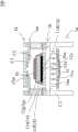
图1A为本案微流体致动器的第一实施例的正面剖面示意图。FIG. 1A is a schematic front cross-sectional view of the first embodiment of the microfluidic actuator of the present invention.
图1B为本案第一实施例的侧面剖面示意图。FIG. 1B is a schematic cross-sectional side view of the first embodiment of the present invention.
图2A至图2AH为本案第一实施例的制造步骤分解示意图。2A to 2AH are exploded schematic views of the manufacturing steps of the first embodiment of the present invention.
图3为本案第一实施例的俯视示意图。FIG. 3 is a schematic top view of the first embodiment of the present invention.
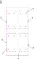
图4为本案第一实施例的入口层的俯视示意图。FIG. 4 is a schematic top view of the inlet layer of the first embodiment of the present invention.
图5为本案第一实施例的流通孔的俯视示意图。FIG. 5 is a schematic top view of the flow hole in the first embodiment of the present invention.
图6A至图6E为本案第一实施例的作动示意图。6A to 6E are schematic diagrams of the operation of the first embodiment of the present invention.
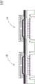
图7A为本案微流体致动器的第二实施例的剖面示意图。FIG. 7A is a schematic cross-sectional view of the second embodiment of the microfluidic actuator of the present invention.
图7B为本案其他实施例的仰视示意图。FIG. 7B is a schematic bottom view of another embodiment of the present invention.
图8为本案第三实施例的阵列孔片的仰视示意图。FIG. 8 is a schematic bottom view of the array hole sheet according to the third embodiment of the present invention.
图9A至图9C为本案第四实施例的翻转对位制程以及晶圆接合制程示意图。9A to 9C are schematic diagrams of a flip alignment process and a wafer bonding process according to the fourth embodiment of the present invention.
附图标记说明Description of reference numerals
100、100'、100"、100'":微流体致动器100, 100', 100", 100'": Microfluidic Actuators
10:致动单元10: Actuating unit
1a、1a'":第一基板1a, 1a'": the first substrate
11a:第一表面11a: first surface
12a:第二表面12a: Second surface
13a:出口沟槽13a: Outlet groove
14a:辅助沟槽14a: Auxiliary groove
15a、15a'":第一出流孔洞15a, 15a'": The first outflow hole
16a、16a'":第二出流孔洞16a, 16a'": the second outflow hole
1b:腔体层1b: Cavity layer
1c:振动层1c: Vibration layer
11c:流体沟槽11c: Fluid Groove
12c:振动区12c: Vibration Zone
1d:第一金属层1d: first metal layer
11d:下电极区11d: Lower electrode area
12d:阻障区12d: Barrier Zone
13d:间隙13d: Gap
1e:压电致动层1e: Piezoelectric Actuation Layer
11e:作动区11e: Action area
1f:隔离层1f: isolation layer
11f:间隙壁11f: Spacer
1g:第二金属层1g: second metal layer
11g:焊垫隔离区11g: Pad isolation area
12g:上电极区12g: Upper electrode area
13g:上电极焊垫13g: Upper electrode pad
14g:下电极焊垫14g: lower electrode pad
1h:防水层1h: Waterproof layer
1i:第二基板1i: Second substrate
1j:薄膜胶层1j: film adhesive layer
1k:入口层1k: entry layer
1m:共振层1m: Resonance layer
11m:腔体通孔11m: cavity through hole
12m:可动部12m: Movable part
13m:固定部13m: Fixed part
1n:罩幕层1n: mask layer
11n:罩幕开口11n: Mask opening
12n:罩幕孔洞12n: mask hole
13n:第一罩幕通孔13n: first mask through hole
14n:第二罩幕通孔14n: second mask through hole
1o、1o'":阵列孔片1o, 1o'": array hole sheet
11o:孔片孔洞11o: Orifice hole
12o、12o'":定位孔12o, 12o'": positioning hole
13o'":支架部13o'": bracket part
AM1:第一接合对位记号AM1: The first joint alignment mark
AM2:第二接合对位记号AM2: Second junction alignment mark
AW:接合对位记号窗AW: Engagement registration mark window
C1:入流腔室C1: Inflow chamber
C2:共振腔室C2: Resonance Chamber
C3:储流腔室C3: Reservoir chamber
I:流体入口I: Fluid inlet
M1:第一光阻层M1: first photoresist layer
M1a:第一光阻区M1a: first photoresist region
M2:第二光阻层M2: Second photoresist layer
M2a:第二光阻孔洞M2a: second photoresist hole
M2b:第二光阻开口M2b: Second photoresist opening
M3:流道层M3: runner layer
M31:流道入口M31: runner inlet
M32:腔体开口M32: cavity opening
M33:入流通道M33: Inflow channel
M4:第三光阻层M4: third photoresist layer
M41:第三光阻开口M41: Third photoresist opening
P、P'":定位柱P, P'": positioning column
具体实施方式Detailed ways
体现本案特征与优点的一些典型实施例将在后段的说明中详细叙述。应理解的是本案能够在不同的态样上具有各种的变化,其皆不脱离本案的范围,且其中的说明及图示在本质上当作说明之用,而非用以限制本案。Some typical embodiments embodying the features and advantages of the present case will be described in detail in the description of the latter paragraph. It should be understood that this case can have various changes in different aspects, all of which do not depart from the scope of this case, and the descriptions and diagrams therein are essentially used for illustration rather than limiting this case.
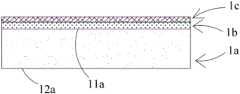
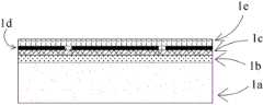
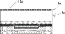
本案的微流体致动器用于输送流体,请参阅图1A以及图1B,于本案实施例中,微流体致动器100包含:一第一基板1a、一腔体层1b、一振动层1c、一第一金属层1d、一压电致动层1e、一隔离层1f、一第二金属层1g、一防水层1h、一第二基板1i、一薄膜胶层1j、一入口层1k、一共振层1m、一罩幕层1n、一阵列孔片1o、一第一光阻层M1、一第二光阻层M2、一流道层M3以及一第三光阻层M4。阵列孔片1o、第一基板1a、腔体层1b、振动层1c、第一金属层1d、压电致动层1e、隔离层1f、第二金属层1g、防水层1h、第二光阻层M2、共振层1m、流道层M3以及入口层1k是依序堆叠结合后形成为一体,其制程如下说明。于本案第一实施例中,微流体致动器100包含一致动单元10。The microfluidic actuator of the present case is used for transporting fluids. Please refer to FIG. 1A and FIG. 1B. In the embodiment of the present case, the
请参阅图2A,于本案第一实施例中,第一基板1a为一硅基材。第一基板1a具有一第一表面11a以及一相对于第一表面11a的第二表面12a。于本案第一实施例中,腔体层1b透过一二氧化硅材料沉积制程形成于第一基板1a的第一表面11a之上,沉积制程可为一物理气相沉积制程(PVD)、一化学气相沉积制程(CVD)或两者的组合,但不以此为限。于本案第一实施例中,振动层1c透过一氮化硅材料沉积制程形成于腔体层1b之上。Please refer to FIG. 2A , in the first embodiment of the present application, the first substrate 1 a is a silicon substrate. The first substrate 1a has a
请参阅图2B以及图3,于本案第一实施例中,振动层1c透过一蚀刻制程形成多个流体沟槽11c以及一振动区12c。流体沟槽11c对称形成于振动层1c的相对两侧,借以定义出振动区12c。值得注意的是,于本案第一实施例中,蚀刻制程可为一湿式蚀刻制程、一干式蚀刻制程或两者的组合,但不以此为限。值得注意的是,于本案第一实施例中,振动层1c,具有二流体沟槽11c,分别形成于振动层1c纵向的相对两侧,但不以此为限。Referring to FIG. 2B and FIG. 3 , in the first embodiment of the present application, the
请参阅图2C以及图2D,于本案第一实施例中,第一金属层1d透过一第一金属材料沉积制程形成于振动层1c之上。于本案实施例中,第一金属材料为一氮化钛金属材料或一钽金属材料,但不以此为限。第一金属层1d透过蚀刻制程形成一下电极区11d、多个阻障区12d、多个间隙13d以及多个第一接合对位记号AM1。下电极区11d形成于对应振动层1c的振动区12c的位置。间隙13d形成于下电极区11d与阻障区12d之间。阻障区12d对应形成于振动层1c的流体沟槽11c的外侧位置。第一接合对位记号AM1形成于阻障区12d之上。Please refer to FIG. 2C and FIG. 2D. In the first embodiment of the present application, the
请参阅图2E以及图2F,于本案第一实施例中,压电致动层1e透过一压电材料沉积制程形成于第一金属层1d之上,且透过蚀刻制程于对应第一金属层1d的下电极区11d的位置形成一作动区11e。Please refer to FIG. 2E and FIG. 2F. In the first embodiment of the present application, the piezoelectric actuating layer 1e is formed on the
请参阅图2G以及图2H,于本案第一实施例中,隔离层1f透过一二氧化硅材料沉积制程形成于第一金属层1d以及压电致动层1e上,且透过蚀刻制程于第一金属层1d之间隙13d内形成多个间隙壁11f。Please refer to FIG. 2G and FIG. 2H. In the first embodiment of the present application, the
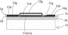
请参阅图2I以及图2J,于本案第一实施例中,第一光阻层M1透过一光阻涂布制程形成于第一金属层1d、压电致动层1e以及隔离层1f上,并透过一显影制程形成一第一光阻区M1a。值得注意的是,光阻涂布制程可为一旋涂(Spin Coating)制程或一层压(LaminateRolling)制程,但不以此为限,得以依照制程需求作变更。于本案第一实施例中,第一光阻层M1为一负光阻,但不以此为限。Please refer to FIGS. 2I and 2J. In the first embodiment of the present application, the first photoresist layer M1 is formed on the
请参阅图2K、图2L以及图3,于本案第一实施例中,第二金属层1g透过一第二金属材料沉积制程形成于第一金属层1d、压电致动层1e、该隔离层1f以及第一光阻层M1的第一光阻区M1a之上。于本案第一实施例中,第二金属材料为一金金属材料或一铝金属材料,但不以此为限。第二金属层1g透过一掀离(Lift-Off)制程将第一光阻层M1移除,借以形成一焊垫隔离区11g、一上电极区12g、一上电极焊垫13g以及一下电极焊垫14g。上电极区12g形成于压电致动层1e的作动区11e之上。上电极焊垫13g以及下电极焊垫14g形成于第一金属层1d之上,并位于压电致动层1e的作动区11e的相对两侧。上电极区12g与下电极焊垫14g借由焊垫隔离区11g相分离。2K , FIG. 2L and FIG. 3 , in the first embodiment of the present application, the
请参阅图2M,于本案第一实施例中,防水层1h透过一镀膜制程形成于第一金属层1d、第二金属层1g以及隔离层1f上,并透过蚀刻制程露出第二金属层1g的上电极焊垫13g以及下电极焊垫14g。值得注意的是,于本案第一实施例中,防水层1h为一聚对二甲苯(Parylene)材质,但不以此为限。聚对二甲苯可于室温下镀膜,并且具有包覆性强、耐化性高以及生物相容性佳等优点。值得注意的是,防水层1h的设置,可避免第一金属层1d、压电致动层1e以及第二金属层1g遭流体腐蚀而产生短路现象。Referring to FIG. 2M, in the first embodiment of the present application, the
请参阅图2N以及图2O,于本案第一实施例中,第二光阻层M2透过光阻涂布制程形成于第一金属层1d、第二金属层1g以及防水层1h上,并透过显影制程形成多个第二光阻孔洞M2a以及一第二光阻开口M2b。2N and FIG. 2O, in the first embodiment of the present application, the second photoresist layer M2 is formed on the
请参阅图2P、图2Q以及图4,于本案第一实施例中,第二基板1i为一玻璃基板。薄膜胶层1j透过一滚压制程形成于第二基板1i上。入口层1k透过滚压制程形成于薄膜胶层1j。于本案第一实施例中,入口层1k为一聚酰亚胺(Polyimide,PI)材质,但不以此为限。薄膜胶层1j以及入口层1k透过蚀刻制程形成多个流体入口I以及多个接合对位记号窗AW。接合对位记号窗AW形成于流体入口I之外侧。值得注意的是,成形流体入口I以及接合对位记号窗AW的蚀刻制程为一干蚀刻制程或一激光蚀刻制程,但不以此为限。于本案第一实施例中,微流体致动器100具有四个流体入口I,分别位于微流体致动器100的四个角落,于其他实施例中,流体入口I的数量以及分布方式得依设计需求而变化。Please refer to FIG. 2P , FIG. 2Q and FIG. 4 , in the first embodiment of the present application, the second substrate 1 i is a glass substrate. The thin film adhesive layer 1j is formed on the second substrate 1i through a rolling process. The
请参阅图2R、图2S以及图4,于本案第一实施例中,流道层M3透过光阻涂布制程形成于入口层1k上,且透过显影制程形成多个流道入口M31、一腔体开口M32以及多个入流通道M33。流道入口M31分别与入口层1k的流体入口I相连通。流道入口M31以及入流通道M33围绕设置在腔体开口M32周围。入流通道M33连通于流道入口M31与腔体开口M32之间。于本案第一实施例中,流道层M3具有四个流道入口M31以及四个入流通道M33,于其他实施例中,流道入口M31以及入流通道M33的数量可以设计需求而变更,不以此为限。于本案第一实施例中,流道层M3为一厚膜光阻,但不以此为限。Please refer to FIGS. 2R, 2S and 4. In the first embodiment of the present application, the flow channel layer M3 is formed on the
请参阅图2T以及图2U,于本案第一实施例中,共振层1m透过滚压制程形成于流道层M3上,且透过蚀刻制程形成一腔体通孔11m以及多个第二接合对位记号AM2。共振层1m覆盖流道层M3的腔体开口M32,借以定义出一入流腔室C1。腔体通孔11m与流道层M3的入流腔室C1相连通。第二接合对位记号AM2形成于共振层1m之外侧。共振层1m自腔体通孔11m向外延伸至对应入流腔室C1外缘处定义为一可动部12m。共振层1m自可动部12m向外延伸至第二接合对位记号AM2处定义为一固定部13m。值得注意的是,成形共振层1m的蚀刻制程为干蚀刻制程或激光蚀刻制程,但不以此为限。Please refer to FIGS. 2T and 2U. In the first embodiment of the present application, the
请参阅图2V,于本案第一实施例中,共振层1m透过一翻转对位制程以及一晶圆接合制程接合于第二光阻层M2上。于翻转对位制程时,利用接合对位记号窗AW与相对应的第一接合对位记号AM1以及相对应的第二接合对位记号AM2相对准,以完成对位制程。值得注意的是,于本案第一实施例中,由于流道层M3以及第二基板1i呈透光性,于翻转对位制程时,可借由正面透视对位(Top-Side Transparent Alignment)方法进行人工对位,因此对位精度需求为±10μm。于本案第一实施例中,共振层1m为一聚酰亚胺(Polyimide,PI)材质,但不以此为限。Referring to FIG. 2V, in the first embodiment of the present application, the
请参阅图2W,于本案第一实施例中,第二基板1i借由将薄膜胶层1j浸泡药剂使薄膜胶层1j失去粘性而移除。值得注意的是,于本案第一实施例中,浸泡薄膜胶层1j所需的时间极短,并且薄膜胶层1j与流道层M3的材质特性不同,因此药剂不会对流道层M3起反应,也不会产生泡胀(Swelling)的问题。Referring to FIG. 2W, in the first embodiment of the present application, the second substrate 1i is removed by soaking the film adhesive layer 1j with a chemical to make the film adhesive layer 1j lose its viscosity. It is worth noting that in the first embodiment of the present case, the time required to soak the film adhesive layer 1j is extremely short, and the material properties of the film adhesive layer 1j and the flow channel layer M3 are different, so the drug will not react to the flow channel layer M3 , and will not have the problem of swelling (Swelling).
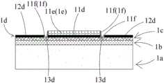
请参阅图2X至图2Z,于本案第一实施例中,罩幕层1n透过一二氧化硅材料沉积制程形成于第一基板1a的第二表面12a上,且透过蚀刻制程形成一罩幕开口11n以及多个罩幕孔洞12n,使得第一基板1a露出。第一基板1a的第二表面12a分别沿着罩幕开口11n以及罩幕孔洞12n,透过蚀刻制程形成一出口沟槽13a以及多个辅助沟槽14a。出口沟槽13a以及辅助沟槽14a具有相同的蚀刻深度,且蚀刻深度为蚀刻至第一表面11a以及第二表面12a之间且不与腔体层1b接触。辅助沟槽14a对称设置在出口沟槽13a的相对两侧。每一辅助沟槽14a与出口沟槽13a之间形成一定位柱P。Referring to FIGS. 2X to 2Z, in the first embodiment of the present application, the mask layer 1n is formed on the
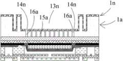
请参阅图2AA及图2AB,于本案第一实施例中,罩幕层1n再透过一二氧化硅材料沉积制程形成于第一基板1a的出口沟槽13a以及辅助沟槽14a内,且透过一精密穿孔制程于出口沟槽13a内形成多个第一罩幕通孔13n以及多个第二罩幕通孔14n。第二罩幕通孔14n对称设置于第一罩幕通孔13n的外侧。于本案第一实施例中,第一罩幕通孔13n的孔径小于第二罩幕通孔14n的孔径,但不以此为限。第一罩幕通孔13n以及第二罩幕通孔14n的穿孔深度为至与第一基板1a接触为止,使得第一基板1a得以露出。于本案第一实施例中,精密穿孔制程为一准分子激光加工制程,但不以此为限。Please refer to FIGS. 2AA and 2AB. In the first embodiment of the present invention, the mask layer 1n is formed in the
请参阅图2AC、图2AD以及图5,于本案第一实施例中,第一基板1a透过一低温深蚀刻制程蚀刻第一基板1a对应于第一罩幕通孔13n以及第二罩幕通孔14n的部分,借以形成第一基板1a的多个第一出流孔洞15a以及多个第二出流孔洞16a。第一出流孔洞15a为分别沿第一罩幕通孔13n蚀刻至与腔体层1b接触为止所构成,以及第二出流孔洞16a为分别沿第二罩幕通孔14n蚀刻至与腔体层1b接触为止所构成。借此,第二出流孔洞16a设置在第一出流孔洞15a的外侧,并且每一第二出流孔洞16a的孔径大于每一第一出流孔洞15a的孔径。于本案第一实施例中,低温深蚀刻制程为一深反应性离子蚀刻制程(BOSCH Process),但不以此为限。于本案第一实施例中,每一第一出流孔洞15a以及每一第二出流孔洞16a具有方形的截面,但不以此为限。2AC, FIG. 2AD and FIG. 5, in the first embodiment of the present application, the first substrate 1a is etched through a low-temperature deep etching process corresponding to the first mask through
值得注意的是,于本案第一实施例中,遮罩层1n利用准分子激光加工制程形成第一罩幕通孔13n以及第二罩幕通孔14n来克服光阻不易涂布以及接触式光罩曝光难以聚焦等问题。此外,于本案第一实施例中,深反应性离子蚀刻制程(BOSCH Process)属于低温制程,可避免加工所产生的高温,影响后端压电材料的极性分布,造成退极化反应。再者,于本案第一实施例中,深反应性离子蚀刻制程(BOSCH Process)所形成的穿孔具有高深宽比(Aspect Ratio),所以穿孔的蚀刻深度以100μm为宜,使得穿孔的孔径可以达到10μm以下,借此维持结构的强度。于本案第一实施例中,出口沟槽13a的设置使得深反应性离子蚀刻制程(BOSCH Process)所形成的穿孔得以降低。It is worth noting that, in the first embodiment of the present application, the mask layer 1n uses an excimer laser processing process to form the first mask through
请参阅图2AD,于本案第一实施例中,腔体层1b再经一湿蚀刻制程于内部蚀刻出一储流腔室C3。意即,透过蚀刻液由第一罩幕通孔13n以及第二罩幕通孔14n流入,经由第一出流孔洞15a以及第二出流孔洞16a流至腔体层1b,进而蚀刻并释放移除腔体层1b的部分,借以定义出储流腔室C3。借此,储流腔室C3与第一出流孔洞15a以及第二出流孔洞16a相连通。值得注意的是,透过湿蚀刻制程成形储流腔室C3的同时,遮罩层1n亦会被一并移除。完成储流腔室C3成形与移除遮罩层1n后,第一出流孔洞15a以及第二出流孔洞16a与出口沟槽13a相连通。Referring to FIG. 2AD, in the first embodiment of the present application, the
值得注意的是,于本案第一实施例中,由于储流腔室C3周围两侧距离略大于出口沟槽13a的两侧距离,因此每一第二出流孔洞16a的孔径大于每一第一出流孔洞15a的孔径的设置有利于储流腔室C3的腔体侧蚀。It should be noted that, in the first embodiment of the present application, since the distance between the two sides of the storage chamber C3 is slightly larger than the distance between the two sides of the
请参阅图2AE至图2AG,于本案第一实施例中,第三光阻层M4透过滚压制程形成于入口层1k上,且透过显影制程形成多个第三光阻开口M41。第三光阻开口M41对应上电极焊垫13g以及下电极焊垫14g的位置而设置。上电极焊垫13g以及下电极焊垫14g透过蚀刻制程移除位于上电极焊垫13g以及下电极焊垫14g上的结构,使得上电极焊垫13g以及下电极焊垫14g得以露出。于本案第一实施例中,第三光阻层M4为一硬遮罩干膜光阻,但不以此为限。值得注意的是,为了避免第一基板1a完成蚀刻后的结构支撑力不足,第三光阻层M4的覆膜也可在完成共振层1m与第二光阻层M2的晶圆接合制程后先进行,但不以此为限。Referring to FIGS. 2AE to 2AG, in the first embodiment of the present application, the third photoresist layer M4 is formed on the
请参阅图2AH以及图5,于本案第一实施例中,阵列孔片1o具有多个孔片孔洞11o以及多个定位孔12o,并透过一粘贴制程贴附于第一基板1a的出口沟槽13a以及辅助沟槽14内。孔片孔洞11o与第一出流孔洞15a以及第二出流孔洞16a相互错位设置,借此封闭第一出流孔洞15a以及第二出流孔洞16a,以构成一单向阀,避免在传输流体时发生流体回流的现象。第一基板1a的定位柱P分别穿过定位孔12o。于本案第一实施例中,第一基板1a的定位柱P的设置使得粘贴阵列孔片1o时可以以人工定位,并借由胶合方式固定,于其他实施例中,阵列孔片1o可以以光学自动对位方式进行定位,如此可增加阵列孔片1o的孔片孔洞11o以及与第一基板1a的第一出流孔洞15a以及第二出流孔洞16a的设置密集度。于本案第一实施例中,每一定位孔12o的孔径大于每一定位柱P的孔径50μm,但不以此为限。于本案第一实施例中,阵列孔片1o为一聚酰亚胺(Polyimide,PI)材质,但不以此为限。于本案第一实施例中,阵列孔片1o具有二定位孔12o,于其他实施例中,定位孔12o的数量可依设计需求而变更,不以此为限。Please refer to FIG. 2AH and FIG. 5. In the first embodiment of the present application, the array hole sheet 1o has a plurality of hole sheet holes 11o and a plurality of positioning holes 12o, and is attached to the outlet groove of the first substrate 1a through a sticking process inside the
请参阅图3,值得注意的是,于本案第一实施例中,振动层1c的二流体沟槽11c分别形成于振动层1c纵向的相对两侧,如此,以振动层1c的横向支撑,可使得振动层1c在纵向有较佳的变形量。Please refer to FIG. 3 , it is worth noting that in the first embodiment of the present application, the two-
请参阅图1A、图1B、图6A至图6E,于本案第一实施例中,微流体致动器100的具体作动方式,是提供具有不同相位电荷的驱动电源至上电极焊垫13g以及下电极焊垫14g,以驱动并控制振动层1c的振动区12c产生上下位移。如图1A以及图6A所示,当施加负电压给上电极焊垫13g以及正电压给下电极焊垫14g时,压电致动层1e的作动区11e带动振动层1c的振动区12c朝向靠近第一基板1a的方向位移。借此,外部流体由流体入口I被吸入至微流体致动器100内,而进入微流体致动器100内的流体接着依序通过流道层M3的流道入口M31、入流通道M33流至入流腔室C1,再通过共振层1m的腔体通孔11m流至内共振腔室C2。如图1A以及图6B所示,停止施加电压给上电极焊垫13g以及下电极焊垫14g,使得压电致动层1e的作动区11e带动振动层1c的振动区12c回复到未被致动的位置。此时,共振层1m的可动部12m因共振而位移,朝向靠近第一基板1a的方向位移并贴附于防水层1h上,使得共振层1m的腔体通孔11m与共振腔室C2不连通。借此,共振腔室C2内的流体被挤压后通过振动层1c的流体沟槽11c汇入腔体层1b的储流腔室C3内。如图1A以及图6C所示,接着转换上电极焊垫13g以及下电极焊垫14g的电性,施加正电压给上电极焊垫13g以及负电压给下电极焊垫14g,如此振动层1c的振动区12c朝向远离第一基板1a的方向位移,以及共振层1m的可动部12m回复到未产生共振位移时的位置,使共振腔室C2内体积受振动层1c压缩,致使汇集于储流腔室C3内的流体开始注入第一出流孔洞15a以及第二出流孔洞16a。如图1A以及图6D所示,再停止施加电压给上电极焊垫13g以及下电极焊垫14g,使得压电致动层1e的作动区11e带动振动层1c的振动区12c回复到未被致动的位置。此时,共振层1m的可动部12m因共振而位移,朝向远离第一基板1a的方向位移并贴附于入口层1k上,使得共振层1m的腔体通孔11m与入流腔室C1不连通。借此,储流腔室C3内的流体被挤压后通过第一出流孔洞15a以及第二出流孔洞16a后推开阵列孔片1o。如图1A以及图6E所示,当共振层1m的可动部12m停止共振并回复到未产生共振位移时的位置,流体通过阵列孔片1o的孔片孔洞11o后排出于微流体致动器100外,以完成流体的传输。Please refer to FIG. 1A , FIG. 1B , FIGS. 6A to 6E , in the first embodiment of the present application, the specific operation mode of the
请参阅图7A,本案第二实施例与第一实施例大致相同,不同之处在于微流体致动器100'包含二个致动单元10,借以增加流量输出。Referring to FIG. 7A , the second embodiment of the present application is substantially the same as the first embodiment, except that the
请参阅图7B,于本案其他实施例中,微流体致动器100"包含多个致动单元10。多个致动单元10可借串联、并联或串并联方式设置,借以增加流量输出,多个致动单元10的设置方式可依照使用需求而设计,不以此为限。Please refer to FIG. 7B , in other embodiments of the present application, the
请参阅图8,本案第三实施例与第一实施例大致相同,不同之处在于微流体致动器100'"的定位柱P'"以及阵列孔片1o'"的定位孔12o'"对称设置于第一基板1a”'的相对角落,并且每一第一出流孔洞15a'"以及每一第二出流孔洞16a'"具有一圆形截面。此外,阵列孔片1o'"具有一支架部13o'",用以增加阵列孔片1o'"的伸张量,达到一弹簧的效果。于本案第三实施例中,阵列孔片1o'"可用以过滤流体中的杂质,增加微流体致动器100'"中元件的可靠性及使用寿命。Please refer to FIG. 8 , the third embodiment of the present case is substantially the same as the first embodiment, except that the positioning posts P''' of the microfluidic actuator 100''' and the positioning holes 12o''' of the array hole sheet 1o''' are symmetrical are disposed at opposite corners of the first substrate 1a"', and each of the
请参阅图9A至图9C,本案第四实施例与第一实施例大致相同,不同之处在于翻转对位制程以及晶圆接合制程不同。由于第一基板1a与第二基板1i的热传导差异大,加上晶圆接合制程易有热应力及气泡(Void)等问题发生,因此,先成形第一基板1a、腔体层1b、振动层1c、第一金属层1d、压电致动层1e、隔离层1f、第二金属层1g、防水层1h、第二光阻层M2以及共振层1m成为一单颗半成品后,再另外于入口层1k上进行滚压及显影制程成形流道层M3,最后翻转入口层1k及流道层M3以覆晶(Flip Chip)方式与前述单颗半成品进行光学双面对位完成接合。此外,为了减少第一基板1a经过蚀刻制程后产生脆裂的可能,可先于接合表面进行活性处理,借此降低热压时的压力。于本案第四实施例中,入口层1k为一电铸或不锈钢材质,借以增加入口层1k的刚性,但不以此为限。Referring to FIGS. 9A to 9C , the fourth embodiment of the present application is substantially the same as the first embodiment, except that the flip alignment process and the wafer bonding process are different. Due to the large difference in thermal conductivity between the first substrate 1a and the second substrate 1i, and problems such as thermal stress and voids are likely to occur in the wafer bonding process, the first substrate 1a, the
本案提供一微流体致动器,主要以微机电制程来完成的微流体致动器,并且借由施加不同相位电荷的驱动电源于上电极焊垫以及下电极焊垫,使得振动层的振动区产生上下位移,进而达到流体传输。此外,借由贴覆一阵裂孔片于出流孔洞上,作为一单向阀,避免流体回流现象发生,极具产业的利用价值,依法提出申请。This application provides a microfluidic actuator, which is mainly completed by a micro-electromechanical process, and by applying driving power sources with different phase charges to the upper electrode pad and the lower electrode pad, the vibration area of the vibration layer is made. Up and down displacement is generated to achieve fluid transmission. In addition, by sticking a burst of perforated sheet on the outflow hole, it acts as a one-way valve to avoid the occurrence of fluid backflow, which is of great industrial value.
本案得由熟知此技术的人士任施匠思而为诸般修饰,然皆不脱如附申请专利范围所欲保护者。This case can be modified by Shi Jiangsi, a person who is familiar with this technology, but all of them do not deviate from the protection of the scope of the patent application attached.
Claims (23)
Priority Applications (1)
| Application Number | Priority Date | Filing Date | Title |
|---|---|---|---|
| CN201910034831.3ACN111434603B (en) | 2019-01-15 | 2019-01-15 | Microfluidic Actuators |
Applications Claiming Priority (1)
| Application Number | Priority Date | Filing Date | Title |
|---|---|---|---|
| CN201910034831.3ACN111434603B (en) | 2019-01-15 | 2019-01-15 | Microfluidic Actuators |
Publications (2)
| Publication Number | Publication Date |
|---|---|
| CN111434603Atrue CN111434603A (en) | 2020-07-21 |
| CN111434603B CN111434603B (en) | 2025-05-27 |
Family
ID=71580700
Family Applications (1)
| Application Number | Title | Priority Date | Filing Date |
|---|---|---|---|
| CN201910034831.3AActiveCN111434603B (en) | 2019-01-15 | 2019-01-15 | Microfluidic Actuators |
Country Status (1)
| Country | Link |
|---|---|
| CN (1) | CN111434603B (en) |
Citations (15)
| Publication number | Priority date | Publication date | Assignee | Title |
|---|---|---|---|---|
| US4826131A (en)* | 1988-08-22 | 1989-05-02 | Ford Motor Company | Electrically controllable valve etched from silicon substrates |
| JP2005299597A (en)* | 2004-04-15 | 2005-10-27 | Tama Tlo Kk | Micro pump |
| JP2010064260A (en)* | 2008-09-08 | 2010-03-25 | Ricoh Co Ltd | Liquid ejection head and method for manufacturing the same, image forming apparatus |
| CN102979705A (en)* | 2011-09-06 | 2013-03-20 | 株式会社村田制作所 | Fluid control device |
| TWM465471U (en)* | 2013-06-24 | 2013-11-11 | Microjet Technology Co Ltd | Micro-gas transmission apparatus |
| TW201500668A (en)* | 2013-06-24 | 2015-01-01 | Microjet Technology Co Ltd | Micro-gas transmission apparatus |
| TWM541542U (en)* | 2017-01-13 | 2017-05-11 | 研能科技股份有限公司 | Micro-gas pressure driving apparatus |
| TWM542099U (en)* | 2017-01-05 | 2017-05-21 | 研能科技股份有限公司 | Fluid control device |
| CN106926582A (en)* | 2015-12-29 | 2017-07-07 | 意法半导体股份有限公司 | Improved manufacturing method for fluid ejection device and fluid ejection device |
| CN107023456A (en)* | 2016-01-29 | 2017-08-08 | 研能科技股份有限公司 | Micro fluid control device |
| TWM553321U (en)* | 2017-08-31 | 2017-12-21 | Microjet Technology Co Ltd | Microelectromechanical fluid control device |
| CN107795465A (en)* | 2016-09-05 | 2018-03-13 | 研能科技股份有限公司 | Micro fluid control device |
| TW201808778A (en)* | 2016-09-05 | 2018-03-16 | 研能科技股份有限公司 | Micro-fluid control device |
| CN108302015A (en)* | 2017-01-13 | 2018-07-20 | 研能科技股份有限公司 | Micro fluid control device |
| CN209583627U (en)* | 2019-01-15 | 2019-11-05 | 研能科技股份有限公司 | microfluidic actuator |
- 2019
- 2019-01-15CNCN201910034831.3Apatent/CN111434603B/enactiveActive
Patent Citations (15)
| Publication number | Priority date | Publication date | Assignee | Title |
|---|---|---|---|---|
| US4826131A (en)* | 1988-08-22 | 1989-05-02 | Ford Motor Company | Electrically controllable valve etched from silicon substrates |
| JP2005299597A (en)* | 2004-04-15 | 2005-10-27 | Tama Tlo Kk | Micro pump |
| JP2010064260A (en)* | 2008-09-08 | 2010-03-25 | Ricoh Co Ltd | Liquid ejection head and method for manufacturing the same, image forming apparatus |
| CN102979705A (en)* | 2011-09-06 | 2013-03-20 | 株式会社村田制作所 | Fluid control device |
| TWM465471U (en)* | 2013-06-24 | 2013-11-11 | Microjet Technology Co Ltd | Micro-gas transmission apparatus |
| TW201500668A (en)* | 2013-06-24 | 2015-01-01 | Microjet Technology Co Ltd | Micro-gas transmission apparatus |
| CN106926582A (en)* | 2015-12-29 | 2017-07-07 | 意法半导体股份有限公司 | Improved manufacturing method for fluid ejection device and fluid ejection device |
| CN107023456A (en)* | 2016-01-29 | 2017-08-08 | 研能科技股份有限公司 | Micro fluid control device |
| CN107795465A (en)* | 2016-09-05 | 2018-03-13 | 研能科技股份有限公司 | Micro fluid control device |
| TW201808778A (en)* | 2016-09-05 | 2018-03-16 | 研能科技股份有限公司 | Micro-fluid control device |
| TWM542099U (en)* | 2017-01-05 | 2017-05-21 | 研能科技股份有限公司 | Fluid control device |
| TWM541542U (en)* | 2017-01-13 | 2017-05-11 | 研能科技股份有限公司 | Micro-gas pressure driving apparatus |
| CN108302015A (en)* | 2017-01-13 | 2018-07-20 | 研能科技股份有限公司 | Micro fluid control device |
| TWM553321U (en)* | 2017-08-31 | 2017-12-21 | Microjet Technology Co Ltd | Microelectromechanical fluid control device |
| CN209583627U (en)* | 2019-01-15 | 2019-11-05 | 研能科技股份有限公司 | microfluidic actuator |
Also Published As
| Publication number | Publication date |
|---|---|
| CN111434603B (en) | 2025-05-27 |
Similar Documents
| Publication | Publication Date | Title |
|---|---|---|
| TWI695120B (en) | Micro fluid actuator | |
| KR101153613B1 (en) | Micro-ejector and method for manufacturing the same | |
| CN209940465U (en) | Microfluidic actuator | |
| CN209583627U (en) | microfluidic actuator | |
| CN209098182U (en) | Microfluidic actuator | |
| TWI666165B (en) | Manufacturing method of micro fluid actuator | |
| TWI722339B (en) | Micro fluid actuator | |
| TWM580642U (en) | Miniature fluid actuator | |
| KR20070067988A (en) | Manufacturing method of microfluidic device and microfluidic device manufactured thereby | |
| TWI713142B (en) | Manufacturing method of miniature fluid actuator | |
| TWI707487B (en) | Manufacturing method of micro fluid actuator | |
| TWM582072U (en) | Microfluidic actuator module | |
| CN111434603A (en) | Microfluidic actuator | |
| CN111750142B (en) | Microfluidic actuator module | |
| CN111217317B (en) | Method for manufacturing microfluidic actuator | |
| CN111434386B (en) | Fabrication method of microfluidic actuator | |
| TWI678819B (en) | Manufacturing method of micro fluid actuator | |
| TWM576620U (en) | Miniature fluid actuator | |
| CN210003874U (en) | Microfluidic actuator module | |
| CN112808330B (en) | Fabrication method of microfluidic actuator | |
| CN111254390B (en) | Method for manufacturing micro-fluid actuator | |
| TWI710517B (en) | Micro fluid actuator | |
| CN111252727A (en) | Microfluidic actuator | |
| TW202036942A (en) | Manufacturing method of micro fluid actuator module | |
| Yunas et al. | Investigation of simple process technology for the fabrication of valveless micropumps |
Legal Events
| Date | Code | Title | Description |
|---|---|---|---|
| PB01 | Publication | ||
| PB01 | Publication | ||
| SE01 | Entry into force of request for substantive examination | ||
| SE01 | Entry into force of request for substantive examination | ||
| GR01 | Patent grant | ||
| GR01 | Patent grant |